EP3522202B1 - Verfahren zur herstellung eines soi-wafers - Google Patents
Verfahren zur herstellung eines soi-wafers Download PDFInfo
- Publication number
- EP3522202B1 EP3522202B1 EP17855481.2A EP17855481A EP3522202B1 EP 3522202 B1 EP3522202 B1 EP 3522202B1 EP 17855481 A EP17855481 A EP 17855481A EP 3522202 B1 EP3522202 B1 EP 3522202B1
- Authority
- EP
- European Patent Office
- Prior art keywords
- wafer
- bonded soi
- wafers
- heat treatment
- oxide film
- Prior art date
- Legal status (The legal status is an assumption and is not a legal conclusion. Google has not performed a legal analysis and makes no representation as to the accuracy of the status listed.)
- Active
Links
Images
Classifications
-
- H—ELECTRICITY
- H10—SEMICONDUCTOR DEVICES; ELECTRIC SOLID-STATE DEVICES NOT OTHERWISE PROVIDED FOR
- H10P—GENERIC PROCESSES OR APPARATUS FOR THE MANUFACTURE OR TREATMENT OF DEVICES COVERED BY CLASS H10
- H10P10/00—Bonding of wafers, substrates or parts of devices
- H10P10/12—Bonding of semiconductor wafers or semiconductor substrates to semiconductor wafers or semiconductor substrates
-
- H—ELECTRICITY
- H10—SEMICONDUCTOR DEVICES; ELECTRIC SOLID-STATE DEVICES NOT OTHERWISE PROVIDED FOR
- H10P—GENERIC PROCESSES OR APPARATUS FOR THE MANUFACTURE OR TREATMENT OF DEVICES COVERED BY CLASS H10
- H10P90/00—Preparation of wafers not covered by a single main group of this subclass, e.g. wafer reinforcement
- H10P90/19—Preparing inhomogeneous wafers
- H10P90/1904—Preparing vertically inhomogeneous wafers
- H10P90/1906—Preparing SOI wafers
- H10P90/1914—Preparing SOI wafers using bonding
- H10P90/1916—Preparing SOI wafers using bonding with separation or delamination along an ion implanted layer, e.g. Smart-cut
-
- H—ELECTRICITY
- H10—SEMICONDUCTOR DEVICES; ELECTRIC SOLID-STATE DEVICES NOT OTHERWISE PROVIDED FOR
- H10D—INORGANIC ELECTRIC SEMICONDUCTOR DEVICES
- H10D86/00—Integrated devices formed in or on insulating or conducting substrates, e.g. formed in silicon-on-insulator [SOI] substrates or on stainless steel or glass substrates
-
- H—ELECTRICITY
- H10—SEMICONDUCTOR DEVICES; ELECTRIC SOLID-STATE DEVICES NOT OTHERWISE PROVIDED FOR
- H10P—GENERIC PROCESSES OR APPARATUS FOR THE MANUFACTURE OR TREATMENT OF DEVICES COVERED BY CLASS H10
- H10P14/00—Formation of materials, e.g. in the shape of layers or pillars
- H10P14/20—Formation of materials, e.g. in the shape of layers or pillars of semiconductor materials
- H10P14/34—Deposited materials, e.g. layers
- H10P14/3402—Deposited materials, e.g. layers characterised by the chemical composition
- H10P14/3424—Deposited materials, e.g. layers characterised by the chemical composition being Group IIB-VIA materials
- H10P14/3426—Oxides
-
- H—ELECTRICITY
- H10—SEMICONDUCTOR DEVICES; ELECTRIC SOLID-STATE DEVICES NOT OTHERWISE PROVIDED FOR
- H10P—GENERIC PROCESSES OR APPARATUS FOR THE MANUFACTURE OR TREATMENT OF DEVICES COVERED BY CLASS H10
- H10P70/00—Cleaning of wafers, substrates or parts of devices
-
- H—ELECTRICITY
- H10—SEMICONDUCTOR DEVICES; ELECTRIC SOLID-STATE DEVICES NOT OTHERWISE PROVIDED FOR
- H10P—GENERIC PROCESSES OR APPARATUS FOR THE MANUFACTURE OR TREATMENT OF DEVICES COVERED BY CLASS H10
- H10P90/00—Preparation of wafers not covered by a single main group of this subclass, e.g. wafer reinforcement
- H10P90/12—Preparing bulk and homogeneous wafers
- H10P90/129—Preparing bulk and homogeneous wafers by polishing
-
- H—ELECTRICITY
- H10—SEMICONDUCTOR DEVICES; ELECTRIC SOLID-STATE DEVICES NOT OTHERWISE PROVIDED FOR
- H10P—GENERIC PROCESSES OR APPARATUS FOR THE MANUFACTURE OR TREATMENT OF DEVICES COVERED BY CLASS H10
- H10P90/00—Preparation of wafers not covered by a single main group of this subclass, e.g. wafer reinforcement
- H10P90/19—Preparing inhomogeneous wafers
- H10P90/1904—Preparing vertically inhomogeneous wafers
- H10P90/1906—Preparing SOI wafers
-
- H—ELECTRICITY
- H10—SEMICONDUCTOR DEVICES; ELECTRIC SOLID-STATE DEVICES NOT OTHERWISE PROVIDED FOR
- H10P—GENERIC PROCESSES OR APPARATUS FOR THE MANUFACTURE OR TREATMENT OF DEVICES COVERED BY CLASS H10
- H10P95/00—Generic processes or apparatus for manufacture or treatments not covered by the other groups of this subclass
- H10P95/90—Thermal treatments, e.g. annealing or sintering
- H10P95/906—Thermal treatments, e.g. annealing or sintering for altering the shape of semiconductors, e.g. smoothing the surface
-
- H—ELECTRICITY
- H10—SEMICONDUCTOR DEVICES; ELECTRIC SOLID-STATE DEVICES NOT OTHERWISE PROVIDED FOR
- H10W—GENERIC PACKAGES, INTERCONNECTIONS, CONNECTORS OR OTHER CONSTRUCTIONAL DETAILS OF DEVICES COVERED BY CLASS H10
- H10W10/00—Isolation regions in semiconductor bodies between components of integrated devices
- H10W10/10—Isolation regions comprising dielectric materials
- H10W10/181—Semiconductor-on-insulator [SOI] isolation regions, e.g. buried oxide regions of SOI wafers
-
- H—ELECTRICITY
- H10—SEMICONDUCTOR DEVICES; ELECTRIC SOLID-STATE DEVICES NOT OTHERWISE PROVIDED FOR
- H10D—INORGANIC ELECTRIC SEMICONDUCTOR DEVICES
- H10D86/00—Integrated devices formed in or on insulating or conducting substrates, e.g. formed in silicon-on-insulator [SOI] substrates or on stainless steel or glass substrates
- H10D86/01—Manufacture or treatment
-
- H—ELECTRICITY
- H10—SEMICONDUCTOR DEVICES; ELECTRIC SOLID-STATE DEVICES NOT OTHERWISE PROVIDED FOR
- H10D—INORGANIC ELECTRIC SEMICONDUCTOR DEVICES
- H10D86/00—Integrated devices formed in or on insulating or conducting substrates, e.g. formed in silicon-on-insulator [SOI] substrates or on stainless steel or glass substrates
- H10D86/201—Integrated devices formed in or on insulating or conducting substrates, e.g. formed in silicon-on-insulator [SOI] substrates or on stainless steel or glass substrates the substrates comprising an insulating layer on a semiconductor body, e.g. SOI
Definitions
- the present invention relates to a method for manufacturing a bonded SOI wafer.
- SOI Silicon On Insulator
- This SOI wafer has characteristics such as a small parasitic capacitance or high radiation hardness ability since the SOI layer of a substrate surface layer portion which becomes a device fabrication region is electrically separated from the inside of the substrate by the buried insulator layer (a buried oxide film layer (a BOX layer)).
- a BOX layer buried oxide film layer
- EP 2 835 820 A1 describes an atomic-order flat surface treatment method of silicon wafer, wherein dummy wafers are arranged at upper and lower positions of a wafer to be heat-treated, thereby uniformly heating and maintaining the entire surface of the process wafer.
- the SOI wafer having a configuration including a base wafer, a BOX layer, and an SOI layer is generally often manufactured by a bonding method.
- This bonding method is a method of forming a silicon oxide film on, e.g., a surface of at least one of two silicon single crystal wafers, then pressing the two wafers against each other through the formed oxide film, performing a bonding heat treatment to enhance bonding strength, thereafter reducing a thickness of the one wafer (a wafer that forms the SOI layer (which will be referred to as a bond wafer hereinafter)) by mirror polishing or a so-called ion implantation delamination method to manufacture the SOI wafer.
- bonded SOI wafers coping with these use applications are required to have a thick BOX oxide film.
- the bonded SOI wafer includes the thick BOX oxide film, in terms of an upper limit of ion implantation energy, a technique to grow the thick oxide film on a base wafer side and perform bonding is used in some cases.
- a bonded SOI wafer manufacturing process is performed in a state where the thick oxide film is also provided on a back surface side which is opposite to a bonding surface of the base wafer.
- a step of improving flatness of an SOI layer surface after delamination is required.
- this flattening step there are a flattening step which is performed by using CMP (Chemical Mechanical Polishing) and a flattening step based on high-temperature annealing in a hydrogen gas or inert gas atmosphere (which may be referred to as a flattening heat treatment hereinafter).
- CMP Chemical Mechanical Polishing
- a flattening step based on high-temperature annealing in a hydrogen gas or inert gas atmosphere which may be referred to as a flattening heat treatment hereinafter.
- one of these steps is performed to the bonded SOI wafer after delamination.
- Roughness of the SOI layer surface after the flattening step using CMP is equal to that of a mirror-polished wafer, but radial film thickness uniformity of the SOI layer tends to degrade.
- the flattening step based on high-temperature annealing results in roughness slightly higher than that of the mirror-polished wafer, but the film thickness uniformity of the SOI layer is good. In large-diameter wafers each having a diameter of 300 mm or more in particular, degradation of the film thickness uniformity at the flattening step using CMP is considerable. As compared with this, the flattening based on the high-temperature annealing does not have such a tendency.
- Patent Literature 1 As an example of a heat treatment to flatten the SOI layer surface by the high-temperature annealing, there is annealing in an argon atmosphere containing an argon gas which is an inert gas (which may be referred to as an Ar annealing hereinafter) (Patent Literature 1).
- FIG. 1(e) and a paragraph [0047] in Patent Literature 1 have a description that an SOI wafer having an oxide film on a back surface thereof is subjected to a heat treatment in an inert gas atmosphere as the flattening heat treatment, it is preferable to perform the heat treatment at 1200°C or more in case of an argon gas atmosphere (see a paragraph [0048] in Patent Literature 1).
- Patent Literature 1 Japanese Unexamined Patent Application Publication No. 2012-129347
- LPDs Light Point Defects
- the present invention provides a method for manufacturing bonded SOI wafers according to claim 1.
- the silicon wafer used as the dummy wafer is a mirror-polished wafer which has not been used as the dummy wafer or a mirror-polished wafer which has been used as the dummy wafer and then cleaned.
- Such a dummy wafer can be easily prepared, an effect to suppress the increase in LPDs is high, and hence the bonded SOI wafers having less LPDs can be inexpensively manufactured.
- a temperature of the heat treatment in the argon atmosphere is set to 1150°C or more.
- the present invention at the step of performing a heat treatment to each bonded SOI wafer having an oxide film on a back surface thereof in an argon atmosphere in a batch processing heat treatment furnace to flatten a surface of an SOI layer, an increase in LPDs on the SOI layer surface can be suppressed, and a yield of the bonded SOI wafers having less LPDs can be improved.
- the bonded SOI wafers having less LPDs can be stably manufactured.
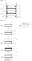
- FIG. 2 is a process flowchart showing an embodiment of a method for manufacturing a bonded SOI wafer according to the present invention. The method for manufacturing a bonded SOI wafer according to the present invention will now be described hereinafter with reference to FIG. 2 .
- a substrate having an oxide film 2 with a thickness of, e.g., 1 ⁇ m on front and back surfaces thereof is prepared ( FIG. 2(a) ).
- the thickness of the oxide film 2 formed here is not restricted in particular as long as it is such a thickness as the oxide film remains on the back surface of the SOI wafer at a flattening heat treatment step which is a later step (f).
- the oxide film 2 can be formed by, e.g., normal thermal oxidation.
- at least one type of ions which is hydrogen ions or a rare gas, can be ion-implanted to a bond wafer 4 to form an ion-implanted layer 3 ( FIG.
- a depth of the ion-implanted layer 3 from a surface of the bond wafer 4 can be set in accordance with a desired thickness of an SOI layer by adjusting a type or energy of ions to be implanted.
- the base wafer 1 having the oxide film 2 formed thereon is bonded to the bond wafer 4 having the ion-implanted layer 3 formed therein through the oxide film 2 in such a manner that the surface of the bond wafer 4 in which the ion-implanted layer 3 has been formed becomes a bonding surface side as shown in FIG. 2(c) (a bonding step).
- pre-bonding cleaning for the base wafer 1 and the bond wafer 4 may be carried out.
- the pre-bonding cleaning for example, RCA cleaning can be used.
- the bond wafer can be delaminated with the ion-implanted layer 3 used as the delamination plane (a delamination step).
- This delamination step enables fabricating a bonded SOI wafer 10 which is constituted of an SOI layer 5 after the delamination, a BOX layer 6 (the oxide film 2), and the base wafer 1 and has the oxide film 2 on the back surface thereof.
- a bond wafer 9 after the delamination is produced as a by-product, but this bond wafer 9 after the delamination can be reproduced as a new bond wafer 4.
- a bonding heat treatment in a high-temperature oxidizing atmosphere may be performed (a bonding heat treatment step).
- a bonding heat treatment step As shown in FIG. 2(e) , a front surface oxide film 7 is formed by the bonding heat treatment on the surface of the SOI layer 5 after the delamination. Then, the front surface oxide film 7 formed by the bonding heat treatment is removed by, e.g., a hydrofluoric acid.
- a sacrificial oxidizing treatment using this oxide film formation and the oxide film removal enables removing mechanical damage caused at the time of the delamination or implantation damage caused at the time of the ion implantation of hydrogen ions or the like.
- the surface roughness is improved by Ar annealing ( FIG. 2(f) , a flattening heat treatment step).
- a heat treatment temperature at this time 1100°C or more can suffice, but it is preferable to set a temperature of the heat treatment in the argon atmosphere to 1150°C or more in the method for manufacturing a bonded SOI wafer according to the present invention.
- a heat treatment temperature is set, migration on the surface of the SOI layer 5 sufficiently advances, and the surface roughness improving effect on the SOI layer 5 of the bonded SOI wafer can be further boosted.
- This heat treatment temperature is more preferably 1200°C or more. When the heat treatment is performed at a higher temperature, the surface roughness can be further improved. Additionally, an upper limit of this heat treatment temperature is not restricted in particular, it is, e.g., 1300°C or less. Although a processing time of the Ar annealing is not restricted in particular, it can be set to three minutes to 10 hours, or more preferably approximately 30 minutes to two hours. This high-temperature Ar annealing processing causes the migration of silicon atoms on the surface of the SOI layer 5, and the surface of the SOI layer 5 is flattened. It is to be noted that the argon atmosphere in the present invention can be an Ar gas 100% atmosphere as well as a non-oxidizing atmosphere mainly containing an Ar gas.
- a silicon wafer 12 is arranged as a dummy wafer between the adjacent bonded SOI wafers 10 housed in the batch processing heat treatment furnace to perform a heat treatment in order to prevent occurrence of the LPDs described above.
- FIG. 1 shows an example of arrangement of the bonded SOI wafers 10 and the dummy wafers (the silicon wafers 12). As shown in FIG.
- each bonded SOI wafer 10 having the oxide film on the back surface thereof is arranged on wafer support portions 13, which are formed on support poles 14 of a boat, every other slot, and each silicon wafer 12 is arranged as the dummy wafer in a slot between the bonded SOI wafers 10.
- each silicon wafer 12 one which does not have the oxide film on the back surface and the front surface thereof is used (a natural oxide film may not be applied thereto).
- the back surface of the silicon wafer 12 having no oxide film is placed immediately above the bonded SOI wafer 10 having the oxide film on the back surface thereof.
- the oxygen component discharged from the back surface of the upper bonded SOI wafer 10 having the oxide film on the back surface thereof is interrupted by the silicon wafer 12 and hardly reaches the front surface of the bonded SOI wafer in the lower slot.
- each mirror-polished wafer 12 arranged between the bonded SOI wafers 10 with a mirror-polished wafer which has not been used as the dummy wafer and has a clean surface in accordance with each batch or after processing a predetermined number of batches, or reuse the clean mirror-polished wafer which has been used as the dummy wafer and then cleaned.
- each mirror-polished wafer can be easily prepared as the dummy wafer and enables inexpensively manufacturing the bonded SOI wafers having less LPDs.
- each slot interval which is used at the time of loading the batch processing heat treatment e.g., an every-two-slot interval, an every-three-slot interval, or an every-four-slot interval
- a technique to simply expand each slot interval which is used at the time of loading the batch processing heat treatment to, e.g., an every-two-slot interval, an every-three-slot interval, or an every-four-slot interval
- it can be considered that suppressing the component which reaches the surface of the lower bonded SOI wafer 10 due to diffusion is difficult.
- productivity of the batch processing heat treatment furnace is considerably impaired.
- a silicon single crystal wafer having both surfaces polished, a diameter of 300 mm, a p conductivity type, a resistivity of 10 ⁇ cm, and a crystal orientation of ⁇ 100> was prepared. Then, an oxide film 2 of 1 ⁇ m was grown on the base wafer 1 at an oxidizing temperature of 950°C. At this time, the oxide film 2 of approximately 1 ⁇ m was also grown on a wafer back surface side.
- This base wafer 1 was bonded to the bond wafer 4 having hydrogen ions implanted with an accelerating voltage of 50 keV and a dosage of 5.0 ⁇ 10 16 /cm 2 , a heat treatment was performed at 500°C for 20 minutes, and delamination was carried out at an ion-implanted layer 3 to fabricate a bonded SOI wafer 10.
- An oxide film of 0.15 ⁇ m was formed at 900°C on the bonded SOI wafer 10 after delamination, and then HF cleaning to remove this film was carried out (a sacrificial oxidizing treatment). Consequently, the bonded wafer 10 having no oxide film on the front surface thereof but having the oxide film of approximately 0.85 ⁇ m on the back surface thereof was obtained.
- a batch processing heat treatment furnace which is a vertical resistance heating type was used to carry out a flattening heat treatment based on inert gas atmosphere annealing (Ar 100%) at 1200°C for one hour.
- 100 bonded SOI wafers 10 to be flattened were arranged on wafer support portions 13 every other slot, and each mirror-polished wafer 12 which had not been used as a dummy wafer and is made of a silicon single crystal was arranged between the bonded SOI wafers 10.
- a sacrificial oxidizing treatment (oxidization at 950°C and removal of the formed oxide films) was performed, and a thickness of each SOI layer was adjusted to 150 nm.
- LPDs each having a diameter of 0.10 ⁇ m or more were measured, and then 84% of the bonded wafers were accepted to an acceptance/rejection standard which is 100 LPDs/wafer or less.
- Bonded SOI wafers 10 were fabricated in 10 continuous batches under the same conditions as those of Example 1. However, in this 10-batch processing, mirror-polished wafers 12 used in the first batch were not cleaned or replaced, and then they were used for a flattening heat treatment in the subsequent nine continuous batches to fabricate the bonded SOI wafers 10. LPD measurement was performed to the bonded SOI wafers 10 fabricated in the 10th batch under the same conditions as those of Example 1, and then 75% of the bonded SOI wafers were accepted.
- Mirror-polished wafers 12 used in the continuous 10-batch processing in Example 2 were cleaned (SC1 cleaning and SC2 cleaning).
- the cleaned mirror-polished wafers 12 were used to perform the first processing to the flattening heat treatment under the same manufacturing conditions as those of Example 1. Further, the LPD measurement was performed under the same conditions as those of Example 1. Consequently, 82% of the bonded SOI wafers were accepted.
- the first processing to a flattening heat treatment were carried out under the same manufacturing conditions as those of Example 1 except that 100 bonded SOI wafers 10 to be flattened were placed on wafer support portions 13 in a batch processing heat treatment furnace without gap at the time of the flattening heat treatment. Further, the LPD measurement was performed under the same conditions as those of Example 1. Consequently, only 2% of the bonded SOI wafers accepted.
- the first processing to a flattening heat treatment were carried out under the same manufacturing conditions as those of Example 1 except that 100 bonded SOI wafers 10 to be flattened were arranged in a boat of a batch processing heat treatment furnace every other slot and each mirror-polished wafer 12 was not arranged between these bonded SOI wafers 10 at the time of the flattening heat treatment. Furthermore, the LPD measurement was performed under the same conditions as those of Example 1, and then only 32% of the bonded SOI wafers were accepted.
- the first processing to a flattening heat treatment were carried out under the same manufacturing conditions as those of Example 1 except that 50 bonded SOI wafers 10 to be flattened were arranged in a boat of a batch processing heat treatment furnace every two slots at expanded wafer intervals and each mirror-polished wafer 12 was not arranged between the bonded SOI wafers 10 at the time of the flattening heat treatment.
- the LPD measurement was performed under the same conditions as those of Example 1, and then only 60% of the bonded SOI wafers were accepted.
- an acceptance rate was higher than those of Comparative Examples 1 and 2 but far lower than those of Examples 1 to 3, and the productivity was reduced as compared with Examples since the number of the bonded SOI wafers 10 to be placed had to be reduced.
- a yield of the bonded SOI wafers with less LPDs was successfully improved. Moreover, the bonded SOI wafers with less LPDs were stably manufactured.
Landscapes
- Element Separation (AREA)
- Mechanical Treatment Of Semiconductor (AREA)
Claims (3)
- Verfahren zur Herstellung gebondeter SOI-Wafer, umfassend:Bereitstellen einer Vielzahl von gebondeten SOI-Wafern (10), jeweils umfassend eine Rückseite und eine Vorderseite, wobei jeder gebondete SOI-Wafer einen Oxidfilm (2) auf der Rückseite und eine SOI-Schicht (5) auf der Vorderseite aufweist;Bereitstellen einer Vielzahl von Silizium-Wafern (12), wobei jeder Silizium-Wafer keinen Oxidfilm auf seiner Rückseite aufweist;Unterbringen der gebondeten SOI-Wafer und der Silizium-Wafer in einer Batch-Verarbeitungskammer (300), wobei jeder Silizium-Wafer als ein Dummy-Wafer verwendet wird, der zwischen jedem der gebondeten SOI-Wafer angeordnet ist; undDurchführen einer Wärmebehandlung in einer Argon-Atmosphäre in der Batch-Verarbeitungskammer an jedem gebondeten SOI-Wafer, um eine vordere Oberfläche der SOI-Schicht plan zu machen.
- Das Verfahren zur Herstellung gebondeter SOI-Wafer gemäß Anspruch 1,
wobei der als Dummy-Wafer verwendete Silizium-Wafer ein hochglanzpolierter Wafer ist, welcher nicht als Dummy-Wafer verwendet wurde, oder ein hochglanzpolierter Wafer, der als Dummy-Wafer verwendet und dann gereinigt wurde. - Das Verfahren zur Herstellung gebondeter SOI-Wafer nach Anspruch 1 oder 2,
wobei eine Temperatur der Wärmebehandlung in der Argon-Atmosphäre auf 1150°C oder mehr eingestellt wird.
Applications Claiming Priority (2)
| Application Number | Priority Date | Filing Date | Title |
|---|---|---|---|
| JP2016188216A JP6531743B2 (ja) | 2016-09-27 | 2016-09-27 | 貼り合わせsoiウェーハの製造方法 |
| PCT/JP2017/029848 WO2018061523A1 (ja) | 2016-09-27 | 2017-08-22 | 貼り合わせsoiウェーハの製造方法 |
Publications (3)
| Publication Number | Publication Date |
|---|---|
| EP3522202A1 EP3522202A1 (de) | 2019-08-07 |
| EP3522202A4 EP3522202A4 (de) | 2020-05-13 |
| EP3522202B1 true EP3522202B1 (de) | 2024-10-02 |
Family
ID=61762769
Family Applications (1)
| Application Number | Title | Priority Date | Filing Date |
|---|---|---|---|
| EP17855481.2A Active EP3522202B1 (de) | 2016-09-27 | 2017-08-22 | Verfahren zur herstellung eines soi-wafers |
Country Status (7)
| Country | Link |
|---|---|
| US (1) | US10600677B2 (de) |
| EP (1) | EP3522202B1 (de) |
| JP (1) | JP6531743B2 (de) |
| KR (1) | KR102408679B1 (de) |
| CN (1) | CN109690733B (de) |
| TW (1) | TWI716627B (de) |
| WO (1) | WO2018061523A1 (de) |
Families Citing this family (4)
| Publication number | Priority date | Publication date | Assignee | Title |
|---|---|---|---|---|
| WO2019064384A1 (ja) * | 2017-09-27 | 2019-04-04 | 株式会社Kokusai Electric | 基板処理装置、半導体装置の製造方法及びプログラム |
| JP6927143B2 (ja) * | 2018-05-17 | 2021-08-25 | 信越半導体株式会社 | 貼り合わせsoiウェーハの製造方法 |
| US10935722B1 (en) * | 2019-09-14 | 2021-03-02 | Dong Li | CMOS compatible material platform for photonic integrated circuits |
| CN110739263A (zh) * | 2019-10-28 | 2020-01-31 | 沈阳硅基科技有限公司 | Soi的制造方法 |
Family Cites Families (22)
| Publication number | Priority date | Publication date | Assignee | Title |
|---|---|---|---|---|
| US6156121A (en) * | 1996-12-19 | 2000-12-05 | Tokyo Electron Limited | Wafer boat and film formation method |
| JPH10189465A (ja) * | 1996-12-26 | 1998-07-21 | Dainippon Screen Mfg Co Ltd | 基板の熱処理装置およびそれを備える薄膜形成装置 |
| US6171982B1 (en) | 1997-12-26 | 2001-01-09 | Canon Kabushiki Kaisha | Method and apparatus for heat-treating an SOI substrate and method of preparing an SOI substrate by using the same |
| JPH11251563A (ja) * | 1997-12-26 | 1999-09-17 | Canon Inc | Soi基板の熱処理方法及び熱処理装置並びにそれを用いたsoi基板の作製方法 |
| JP2002353082A (ja) * | 2001-05-28 | 2002-12-06 | Shin Etsu Handotai Co Ltd | 貼り合わせウェーハの製造方法 |
| JP2004186226A (ja) | 2002-11-29 | 2004-07-02 | Shin Etsu Handotai Co Ltd | Soiウエーハの製造方法 |
| US7544583B2 (en) * | 2003-09-08 | 2009-06-09 | Sumco Corporation | SOI wafer and its manufacturing method |
| JP4626175B2 (ja) * | 2004-04-09 | 2011-02-02 | 株式会社Sumco | Soi基板の製造方法 |
| JP4802624B2 (ja) * | 2005-09-07 | 2011-10-26 | 信越半導体株式会社 | 貼り合わせsoiウェーハの製造方法 |
| JP5183969B2 (ja) * | 2007-05-29 | 2013-04-17 | 信越半導体株式会社 | Soiウェーハのシリコン酸化膜形成方法 |
| JP2010040638A (ja) * | 2008-08-01 | 2010-02-18 | Sumco Corp | Soi基板の製造方法 |
| JP5521561B2 (ja) * | 2010-01-12 | 2014-06-18 | 信越半導体株式会社 | 貼り合わせウェーハの製造方法 |
| JP2012059889A (ja) * | 2010-09-08 | 2012-03-22 | Shin Etsu Handotai Co Ltd | 貼り合わせウェーハの製造方法及びウェーハ載置用サセプタ |
| JP5541136B2 (ja) * | 2010-12-15 | 2014-07-09 | 信越半導体株式会社 | 貼り合わせsoiウエーハの製造方法 |
| JP2013048218A (ja) * | 2011-07-22 | 2013-03-07 | Semiconductor Energy Lab Co Ltd | Soi基板の作製方法 |
| CN102543828B (zh) * | 2011-11-02 | 2014-12-10 | 上海华力微电子有限公司 | 一种soi硅片的制备方法 |
| JP2013143407A (ja) * | 2012-01-06 | 2013-07-22 | Shin Etsu Handotai Co Ltd | 貼り合わせsoiウェーハの製造方法 |
| JP5673572B2 (ja) * | 2012-01-24 | 2015-02-18 | 信越半導体株式会社 | 貼り合わせsoiウェーハの製造方法 |
| CN103443910A (zh) * | 2012-04-05 | 2013-12-11 | 国立大学法人东北大学 | 硅晶片的原子级平坦化表面处理方法及热处理装置 |
| JP6036732B2 (ja) * | 2014-03-18 | 2016-11-30 | 信越半導体株式会社 | 貼り合わせウェーハの製造方法 |
| JP2016082093A (ja) * | 2014-10-17 | 2016-05-16 | 信越半導体株式会社 | 貼り合わせウェーハの製造方法 |
| JP2016201454A (ja) * | 2015-04-09 | 2016-12-01 | 信越半導体株式会社 | Soiウェーハの製造方法 |
-
2016
- 2016-09-27 JP JP2016188216A patent/JP6531743B2/ja active Active
-
2017
- 2017-08-22 KR KR1020197008489A patent/KR102408679B1/ko active Active
- 2017-08-22 WO PCT/JP2017/029848 patent/WO2018061523A1/ja not_active Ceased
- 2017-08-22 US US16/331,079 patent/US10600677B2/en active Active
- 2017-08-22 CN CN201780055519.1A patent/CN109690733B/zh active Active
- 2017-08-22 EP EP17855481.2A patent/EP3522202B1/de active Active
- 2017-08-24 TW TW106128752A patent/TWI716627B/zh active
Also Published As
| Publication number | Publication date |
|---|---|
| US10600677B2 (en) | 2020-03-24 |
| KR102408679B1 (ko) | 2022-06-14 |
| TWI716627B (zh) | 2021-01-21 |
| US20190198386A1 (en) | 2019-06-27 |
| JP2018056230A (ja) | 2018-04-05 |
| CN109690733B (zh) | 2022-10-18 |
| TW201824354A (zh) | 2018-07-01 |
| EP3522202A1 (de) | 2019-08-07 |
| CN109690733A (zh) | 2019-04-26 |
| EP3522202A4 (de) | 2020-05-13 |
| JP6531743B2 (ja) | 2019-06-19 |
| KR20190050995A (ko) | 2019-05-14 |
| WO2018061523A1 (ja) | 2018-04-05 |
Similar Documents
| Publication | Publication Date | Title |
|---|---|---|
| KR101340004B1 (ko) | Soi 웨이퍼의 제조방법 | |
| JP5927894B2 (ja) | Soiウェーハの製造方法 | |
| US20060040469A1 (en) | Soi wafer manufacturing method | |
| JP6036732B2 (ja) | 貼り合わせウェーハの製造方法 | |
| EP3309819B1 (de) | Verfahren zur herstellung eines soi-wafers | |
| KR101488667B1 (ko) | Soi 웨이퍼의 실리콘 산화막 형성 방법 | |
| CN104115255B (zh) | 贴合soi晶片的制造方法 | |
| JPWO2005024925A1 (ja) | Soiウェーハの作製方法 | |
| EP3522202B1 (de) | Verfahren zur herstellung eines soi-wafers | |
| JP4419147B2 (ja) | 貼り合わせウェーハの製造方法 | |
| JP5183958B2 (ja) | Soiウエーハの製造方法 | |
| WO2015136834A1 (ja) | 貼り合わせsoiウェーハの製造方法 | |
| TWI549192B (zh) | Method of manufacturing wafers | |
| JP2016201454A (ja) | Soiウェーハの製造方法 | |
| JP5710429B2 (ja) | 貼り合わせウェーハの製造方法 | |
| US7799660B2 (en) | Method for manufacturing SOI substrate | |
| KR20230070027A (ko) | 접합 웨이퍼용의 지지 기판의 제조 방법 및, 접합 웨이퍼용의 지지 기판 | |
| JP2006013179A (ja) | Soiウェーハの製造方法 |
Legal Events
| Date | Code | Title | Description |
|---|---|---|---|
| STAA | Information on the status of an ep patent application or granted ep patent |
Free format text: STATUS: THE INTERNATIONAL PUBLICATION HAS BEEN MADE |
|
| PUAI | Public reference made under article 153(3) epc to a published international application that has entered the european phase |
Free format text: ORIGINAL CODE: 0009012 |
|
| STAA | Information on the status of an ep patent application or granted ep patent |
Free format text: STATUS: REQUEST FOR EXAMINATION WAS MADE |
|
| 17P | Request for examination filed |
Effective date: 20190312 |
|
| AK | Designated contracting states |
Kind code of ref document: A1 Designated state(s): AL AT BE BG CH CY CZ DE DK EE ES FI FR GB GR HR HU IE IS IT LI LT LU LV MC MK MT NL NO PL PT RO RS SE SI SK SM TR |
|
| AX | Request for extension of the european patent |
Extension state: BA ME |
|
| DAV | Request for validation of the european patent (deleted) | ||
| DAX | Request for extension of the european patent (deleted) | ||
| A4 | Supplementary search report drawn up and despatched |
Effective date: 20200414 |
|
| RIC1 | Information provided on ipc code assigned before grant |
Ipc: H01L 21/762 20060101ALI20200406BHEP Ipc: H01L 21/324 20060101AFI20200406BHEP |
|
| STAA | Information on the status of an ep patent application or granted ep patent |
Free format text: STATUS: EXAMINATION IS IN PROGRESS |
|
| 17Q | First examination report despatched |
Effective date: 20220712 |
|
| REG | Reference to a national code |
Ref country code: DE Ref legal event code: R079 Free format text: PREVIOUS MAIN CLASS: H01L0021020000 Ref country code: DE Ref legal event code: R079 Ref document number: 602017085265 Country of ref document: DE Free format text: PREVIOUS MAIN CLASS: H01L0021020000 Ipc: H01L0021762000 |
|
| RIC1 | Information provided on ipc code assigned before grant |
Ipc: H01L 21/324 20060101ALI20240412BHEP Ipc: H01L 21/02 20060101ALI20240412BHEP Ipc: H01L 27/12 20060101ALI20240412BHEP Ipc: H01L 21/84 20060101ALI20240412BHEP Ipc: H01L 21/762 20060101AFI20240412BHEP |
|
| GRAP | Despatch of communication of intention to grant a patent |
Free format text: ORIGINAL CODE: EPIDOSNIGR1 |
|
| STAA | Information on the status of an ep patent application or granted ep patent |
Free format text: STATUS: GRANT OF PATENT IS INTENDED |
|
| INTG | Intention to grant announced |
Effective date: 20240604 |
|
| RIN1 | Information on inventor provided before grant (corrected) |
Inventor name: HAMA, SETSUYA Inventor name: ISHIZUKA, TORU |
|
| GRAS | Grant fee paid |
Free format text: ORIGINAL CODE: EPIDOSNIGR3 |
|
| GRAA | (expected) grant |
Free format text: ORIGINAL CODE: 0009210 |
|
| STAA | Information on the status of an ep patent application or granted ep patent |
Free format text: STATUS: THE PATENT HAS BEEN GRANTED |
|
| AK | Designated contracting states |
Kind code of ref document: B1 Designated state(s): AL AT BE BG CH CY CZ DE DK EE ES FI FR GB GR HR HU IE IS IT LI LT LU LV MC MK MT NL NO PL PT RO RS SE SI SK SM TR |
|
| REG | Reference to a national code |
Ref country code: GB Ref legal event code: FG4D |
|
| REG | Reference to a national code |
Ref country code: CH Ref legal event code: EP |
|
| REG | Reference to a national code |
Ref country code: IE Ref legal event code: FG4D |
|
| REG | Reference to a national code |
Ref country code: DE Ref legal event code: R096 Ref document number: 602017085265 Country of ref document: DE |
|
| REG | Reference to a national code |
Ref country code: LT Ref legal event code: MG9D |
|
| REG | Reference to a national code |
Ref country code: NL Ref legal event code: MP Effective date: 20241002 |
|
| REG | Reference to a national code |
Ref country code: AT Ref legal event code: MK05 Ref document number: 1729106 Country of ref document: AT Kind code of ref document: T Effective date: 20241002 |
|
| PG25 | Lapsed in a contracting state [announced via postgrant information from national office to epo] |
Ref country code: NL Free format text: LAPSE BECAUSE OF FAILURE TO SUBMIT A TRANSLATION OF THE DESCRIPTION OR TO PAY THE FEE WITHIN THE PRESCRIBED TIME-LIMIT Effective date: 20241002 |
|
| PG25 | Lapsed in a contracting state [announced via postgrant information from national office to epo] |
Ref country code: NL Free format text: LAPSE BECAUSE OF FAILURE TO SUBMIT A TRANSLATION OF THE DESCRIPTION OR TO PAY THE FEE WITHIN THE PRESCRIBED TIME-LIMIT Effective date: 20241002 |
|
| PG25 | Lapsed in a contracting state [announced via postgrant information from national office to epo] |
Ref country code: IS Free format text: LAPSE BECAUSE OF FAILURE TO SUBMIT A TRANSLATION OF THE DESCRIPTION OR TO PAY THE FEE WITHIN THE PRESCRIBED TIME-LIMIT Effective date: 20250202 Ref country code: PT Free format text: LAPSE BECAUSE OF FAILURE TO SUBMIT A TRANSLATION OF THE DESCRIPTION OR TO PAY THE FEE WITHIN THE PRESCRIBED TIME-LIMIT Effective date: 20250203 Ref country code: HR Free format text: LAPSE BECAUSE OF FAILURE TO SUBMIT A TRANSLATION OF THE DESCRIPTION OR TO PAY THE FEE WITHIN THE PRESCRIBED TIME-LIMIT Effective date: 20241002 |
|
| PG25 | Lapsed in a contracting state [announced via postgrant information from national office to epo] |
Ref country code: FI Free format text: LAPSE BECAUSE OF FAILURE TO SUBMIT A TRANSLATION OF THE DESCRIPTION OR TO PAY THE FEE WITHIN THE PRESCRIBED TIME-LIMIT Effective date: 20241002 |
|
| PG25 | Lapsed in a contracting state [announced via postgrant information from national office to epo] |
Ref country code: BG Free format text: LAPSE BECAUSE OF FAILURE TO SUBMIT A TRANSLATION OF THE DESCRIPTION OR TO PAY THE FEE WITHIN THE PRESCRIBED TIME-LIMIT Effective date: 20241002 |
|
| PG25 | Lapsed in a contracting state [announced via postgrant information from national office to epo] |
Ref country code: ES Free format text: LAPSE BECAUSE OF FAILURE TO SUBMIT A TRANSLATION OF THE DESCRIPTION OR TO PAY THE FEE WITHIN THE PRESCRIBED TIME-LIMIT Effective date: 20241002 |
|
| PG25 | Lapsed in a contracting state [announced via postgrant information from national office to epo] |
Ref country code: NO Free format text: LAPSE BECAUSE OF FAILURE TO SUBMIT A TRANSLATION OF THE DESCRIPTION OR TO PAY THE FEE WITHIN THE PRESCRIBED TIME-LIMIT Effective date: 20250102 |
|
| PG25 | Lapsed in a contracting state [announced via postgrant information from national office to epo] |
Ref country code: LV Free format text: LAPSE BECAUSE OF FAILURE TO SUBMIT A TRANSLATION OF THE DESCRIPTION OR TO PAY THE FEE WITHIN THE PRESCRIBED TIME-LIMIT Effective date: 20241002 Ref country code: AT Free format text: LAPSE BECAUSE OF FAILURE TO SUBMIT A TRANSLATION OF THE DESCRIPTION OR TO PAY THE FEE WITHIN THE PRESCRIBED TIME-LIMIT Effective date: 20241002 Ref country code: GR Free format text: LAPSE BECAUSE OF FAILURE TO SUBMIT A TRANSLATION OF THE DESCRIPTION OR TO PAY THE FEE WITHIN THE PRESCRIBED TIME-LIMIT Effective date: 20250103 |
|
| PG25 | Lapsed in a contracting state [announced via postgrant information from national office to epo] |
Ref country code: CZ Free format text: LAPSE BECAUSE OF FAILURE TO SUBMIT A TRANSLATION OF THE DESCRIPTION OR TO PAY THE FEE WITHIN THE PRESCRIBED TIME-LIMIT Effective date: 20241002 Ref country code: PL Free format text: LAPSE BECAUSE OF FAILURE TO SUBMIT A TRANSLATION OF THE DESCRIPTION OR TO PAY THE FEE WITHIN THE PRESCRIBED TIME-LIMIT Effective date: 20241002 |
|
| PG25 | Lapsed in a contracting state [announced via postgrant information from national office to epo] |
Ref country code: RS Free format text: LAPSE BECAUSE OF FAILURE TO SUBMIT A TRANSLATION OF THE DESCRIPTION OR TO PAY THE FEE WITHIN THE PRESCRIBED TIME-LIMIT Effective date: 20250102 |
|
| PG25 | Lapsed in a contracting state [announced via postgrant information from national office to epo] |
Ref country code: SM Free format text: LAPSE BECAUSE OF FAILURE TO SUBMIT A TRANSLATION OF THE DESCRIPTION OR TO PAY THE FEE WITHIN THE PRESCRIBED TIME-LIMIT Effective date: 20241002 |
|
| REG | Reference to a national code |
Ref country code: DE Ref legal event code: R097 Ref document number: 602017085265 Country of ref document: DE |
|
| PG25 | Lapsed in a contracting state [announced via postgrant information from national office to epo] |
Ref country code: DK Free format text: LAPSE BECAUSE OF FAILURE TO SUBMIT A TRANSLATION OF THE DESCRIPTION OR TO PAY THE FEE WITHIN THE PRESCRIBED TIME-LIMIT Effective date: 20241002 |
|
| PG25 | Lapsed in a contracting state [announced via postgrant information from national office to epo] |
Ref country code: EE Free format text: LAPSE BECAUSE OF FAILURE TO SUBMIT A TRANSLATION OF THE DESCRIPTION OR TO PAY THE FEE WITHIN THE PRESCRIBED TIME-LIMIT Effective date: 20241002 |
|
| PG25 | Lapsed in a contracting state [announced via postgrant information from national office to epo] |
Ref country code: RO Free format text: LAPSE BECAUSE OF FAILURE TO SUBMIT A TRANSLATION OF THE DESCRIPTION OR TO PAY THE FEE WITHIN THE PRESCRIBED TIME-LIMIT Effective date: 20241002 |
|
| PG25 | Lapsed in a contracting state [announced via postgrant information from national office to epo] |
Ref country code: SK Free format text: LAPSE BECAUSE OF FAILURE TO SUBMIT A TRANSLATION OF THE DESCRIPTION OR TO PAY THE FEE WITHIN THE PRESCRIBED TIME-LIMIT Effective date: 20241002 |
|
| PG25 | Lapsed in a contracting state [announced via postgrant information from national office to epo] |
Ref country code: IT Free format text: LAPSE BECAUSE OF FAILURE TO SUBMIT A TRANSLATION OF THE DESCRIPTION OR TO PAY THE FEE WITHIN THE PRESCRIBED TIME-LIMIT Effective date: 20241002 |
|
| PLBE | No opposition filed within time limit |
Free format text: ORIGINAL CODE: 0009261 |
|
| STAA | Information on the status of an ep patent application or granted ep patent |
Free format text: STATUS: NO OPPOSITION FILED WITHIN TIME LIMIT |
|
| PG25 | Lapsed in a contracting state [announced via postgrant information from national office to epo] |
Ref country code: SE Free format text: LAPSE BECAUSE OF FAILURE TO SUBMIT A TRANSLATION OF THE DESCRIPTION OR TO PAY THE FEE WITHIN THE PRESCRIBED TIME-LIMIT Effective date: 20241002 |
|
| 26N | No opposition filed |
Effective date: 20250703 |
|
| PGFP | Annual fee paid to national office [announced via postgrant information from national office to epo] |
Ref country code: DE Payment date: 20250820 Year of fee payment: 9 |
|
| PGFP | Annual fee paid to national office [announced via postgrant information from national office to epo] |
Ref country code: FR Payment date: 20250828 Year of fee payment: 9 |
|
| REG | Reference to a national code |
Ref country code: DE Ref legal event code: R079 Ref document number: 602017085265 Country of ref document: DE Free format text: PREVIOUS MAIN CLASS: H01L0021762000 Ipc: H10W0010100000 |
|
| REG | Reference to a national code |
Ref country code: CH Ref legal event code: H13 Free format text: ST27 STATUS EVENT CODE: U-0-0-H10-H13 (AS PROVIDED BY THE NATIONAL OFFICE) Effective date: 20260324 |