EP3491082B1 - Copper ink and conductive solderable copper traces produced therefrom - Google Patents
Copper ink and conductive solderable copper traces produced therefrom Download PDFInfo
- Publication number
- EP3491082B1 EP3491082B1 EP17833137.7A EP17833137A EP3491082B1 EP 3491082 B1 EP3491082 B1 EP 3491082B1 EP 17833137 A EP17833137 A EP 17833137A EP 3491082 B1 EP3491082 B1 EP 3491082B1
- Authority
- EP
- European Patent Office
- Prior art keywords
- copper
- ink
- mil
- substrate
- traces
- Prior art date
- Legal status (The legal status is an assumption and is not a legal conclusion. Google has not performed a legal analysis and makes no representation as to the accuracy of the status listed.)
- Active
Links
Images

Classifications
-
- B—PERFORMING OPERATIONS; TRANSPORTING
- B41—PRINTING; LINING MACHINES; TYPEWRITERS; STAMPS
- B41M—PRINTING, DUPLICATING, MARKING, OR COPYING PROCESSES; COLOUR PRINTING
- B41M3/00—Printing processes to produce particular kinds of printed work, e.g. patterns
- B41M3/006—Patterns of chemical products used for a specific purpose, e.g. pesticides, perfumes, adhesive patterns; use of microencapsulated material; Printing on smoking articles
-
- B—PERFORMING OPERATIONS; TRANSPORTING
- B41—PRINTING; LINING MACHINES; TYPEWRITERS; STAMPS
- B41M—PRINTING, DUPLICATING, MARKING, OR COPYING PROCESSES; COLOUR PRINTING
- B41M7/00—After-treatment of prints, e.g. heating, irradiating, setting of the ink, protection of the printed stock
- B41M7/009—After-treatment of prints, e.g. heating, irradiating, setting of the ink, protection of the printed stock using thermal means, e.g. infrared radiation, heat
-
- C—CHEMISTRY; METALLURGY
- C08—ORGANIC MACROMOLECULAR COMPOUNDS; THEIR PREPARATION OR CHEMICAL WORKING-UP; COMPOSITIONS BASED THEREON
- C08J—WORKING-UP; GENERAL PROCESSES OF COMPOUNDING; AFTER-TREATMENT NOT COVERED BY SUBCLASSES C08B, C08C, C08F, C08G or C08H
- C08J7/00—Chemical treatment or coating of shaped articles made of macromolecular substances
- C08J7/04—Coating
- C08J7/0427—Coating with only one layer of a composition containing a polymer binder
-
- C—CHEMISTRY; METALLURGY
- C09—DYES; PAINTS; POLISHES; NATURAL RESINS; ADHESIVES; COMPOSITIONS NOT OTHERWISE PROVIDED FOR; APPLICATIONS OF MATERIALS NOT OTHERWISE PROVIDED FOR
- C09D—COATING COMPOSITIONS, e.g. PAINTS, VARNISHES OR LACQUERS; FILLING PASTES; CHEMICAL PAINT OR INK REMOVERS; INKS; CORRECTING FLUIDS; WOODSTAINS; PASTES OR SOLIDS FOR COLOURING OR PRINTING; USE OF MATERIALS THEREFOR
- C09D11/00—Inks
- C09D11/02—Printing inks
- C09D11/03—Printing inks characterised by features other than the chemical nature of the binder
- C09D11/037—Printing inks characterised by features other than the chemical nature of the binder characterised by the pigment
-
- C—CHEMISTRY; METALLURGY
- C09—DYES; PAINTS; POLISHES; NATURAL RESINS; ADHESIVES; COMPOSITIONS NOT OTHERWISE PROVIDED FOR; APPLICATIONS OF MATERIALS NOT OTHERWISE PROVIDED FOR
- C09D—COATING COMPOSITIONS, e.g. PAINTS, VARNISHES OR LACQUERS; FILLING PASTES; CHEMICAL PAINT OR INK REMOVERS; INKS; CORRECTING FLUIDS; WOODSTAINS; PASTES OR SOLIDS FOR COLOURING OR PRINTING; USE OF MATERIALS THEREFOR
- C09D11/00—Inks
- C09D11/02—Printing inks
- C09D11/08—Printing inks based on natural resins
-
- C—CHEMISTRY; METALLURGY
- C09—DYES; PAINTS; POLISHES; NATURAL RESINS; ADHESIVES; COMPOSITIONS NOT OTHERWISE PROVIDED FOR; APPLICATIONS OF MATERIALS NOT OTHERWISE PROVIDED FOR
- C09D—COATING COMPOSITIONS, e.g. PAINTS, VARNISHES OR LACQUERS; FILLING PASTES; CHEMICAL PAINT OR INK REMOVERS; INKS; CORRECTING FLUIDS; WOODSTAINS; PASTES OR SOLIDS FOR COLOURING OR PRINTING; USE OF MATERIALS THEREFOR
- C09D11/00—Inks
- C09D11/02—Printing inks
- C09D11/10—Printing inks based on artificial resins
- C09D11/102—Printing inks based on artificial resins containing macromolecular compounds obtained by reactions other than those only involving unsaturated carbon-to-carbon bonds
- C09D11/103—Printing inks based on artificial resins containing macromolecular compounds obtained by reactions other than those only involving unsaturated carbon-to-carbon bonds of aldehydes, e.g. phenol-formaldehyde resins
-
- C—CHEMISTRY; METALLURGY
- C09—DYES; PAINTS; POLISHES; NATURAL RESINS; ADHESIVES; COMPOSITIONS NOT OTHERWISE PROVIDED FOR; APPLICATIONS OF MATERIALS NOT OTHERWISE PROVIDED FOR
- C09D—COATING COMPOSITIONS, e.g. PAINTS, VARNISHES OR LACQUERS; FILLING PASTES; CHEMICAL PAINT OR INK REMOVERS; INKS; CORRECTING FLUIDS; WOODSTAINS; PASTES OR SOLIDS FOR COLOURING OR PRINTING; USE OF MATERIALS THEREFOR
- C09D11/00—Inks
- C09D11/02—Printing inks
- C09D11/10—Printing inks based on artificial resins
- C09D11/102—Printing inks based on artificial resins containing macromolecular compounds obtained by reactions other than those only involving unsaturated carbon-to-carbon bonds
- C09D11/104—Polyesters
-
- C—CHEMISTRY; METALLURGY
- C09—DYES; PAINTS; POLISHES; NATURAL RESINS; ADHESIVES; COMPOSITIONS NOT OTHERWISE PROVIDED FOR; APPLICATIONS OF MATERIALS NOT OTHERWISE PROVIDED FOR
- C09D—COATING COMPOSITIONS, e.g. PAINTS, VARNISHES OR LACQUERS; FILLING PASTES; CHEMICAL PAINT OR INK REMOVERS; INKS; CORRECTING FLUIDS; WOODSTAINS; PASTES OR SOLIDS FOR COLOURING OR PRINTING; USE OF MATERIALS THEREFOR
- C09D11/00—Inks
- C09D11/02—Printing inks
- C09D11/10—Printing inks based on artificial resins
- C09D11/106—Printing inks based on artificial resins containing macromolecular compounds obtained by reactions only involving carbon-to-carbon unsaturated bonds
- C09D11/107—Printing inks based on artificial resins containing macromolecular compounds obtained by reactions only involving carbon-to-carbon unsaturated bonds from unsaturated acids or derivatives thereof
-
- C—CHEMISTRY; METALLURGY
- C09—DYES; PAINTS; POLISHES; NATURAL RESINS; ADHESIVES; COMPOSITIONS NOT OTHERWISE PROVIDED FOR; APPLICATIONS OF MATERIALS NOT OTHERWISE PROVIDED FOR
- C09D—COATING COMPOSITIONS, e.g. PAINTS, VARNISHES OR LACQUERS; FILLING PASTES; CHEMICAL PAINT OR INK REMOVERS; INKS; CORRECTING FLUIDS; WOODSTAINS; PASTES OR SOLIDS FOR COLOURING OR PRINTING; USE OF MATERIALS THEREFOR
- C09D11/00—Inks
- C09D11/52—Electrically conductive inks
-
- C—CHEMISTRY; METALLURGY
- C08—ORGANIC MACROMOLECULAR COMPOUNDS; THEIR PREPARATION OR CHEMICAL WORKING-UP; COMPOSITIONS BASED THEREON
- C08J—WORKING-UP; GENERAL PROCESSES OF COMPOUNDING; AFTER-TREATMENT NOT COVERED BY SUBCLASSES C08B, C08C, C08F, C08G or C08H
- C08J2367/00—Characterised by the use of polyesters obtained by reactions forming a carboxylic ester link in the main chain; Derivatives of such polymers
- C08J2367/02—Polyesters derived from dicarboxylic acids and dihydroxy compounds
-
- C—CHEMISTRY; METALLURGY
- C08—ORGANIC MACROMOLECULAR COMPOUNDS; THEIR PREPARATION OR CHEMICAL WORKING-UP; COMPOSITIONS BASED THEREON
- C08J—WORKING-UP; GENERAL PROCESSES OF COMPOUNDING; AFTER-TREATMENT NOT COVERED BY SUBCLASSES C08B, C08C, C08F, C08G or C08H
- C08J2379/00—Characterised by the use of macromolecular compounds obtained by reactions forming in the main chain of the macromolecule a linkage containing nitrogen with or without oxygen, or carbon only, not provided for in groups C08J2361/00 - C08J2377/00
- C08J2379/04—Polycondensates having nitrogen-containing heterocyclic rings in the main chain; Polyhydrazides; Polyamide acids or similar polyimide precursors
- C08J2379/08—Polyimides; Polyester-imides; Polyamide-imides; Polyamide acids or similar polyimide precursors
-
- C—CHEMISTRY; METALLURGY
- C08—ORGANIC MACROMOLECULAR COMPOUNDS; THEIR PREPARATION OR CHEMICAL WORKING-UP; COMPOSITIONS BASED THEREON
- C08J—WORKING-UP; GENERAL PROCESSES OF COMPOUNDING; AFTER-TREATMENT NOT COVERED BY SUBCLASSES C08B, C08C, C08F, C08G or C08H
- C08J2467/00—Characterised by the use of polyesters obtained by reactions forming a carboxylic ester link in the main chain; Derivatives of such polymers
Definitions
- This application relates to inks, in particular to printable copper inks.
- the main causes of failure during lead-free soldering on copper traces are high sheet resistivity, poor adhesion strength and reduction in wettability caused by oxidation of the surface of the copper trace. Also, good wettability is limited due to heterogeneity (mixtures of copper metal and voids), high surface roughness and poor mechanical strength.
- conductive thick films comprising silver-coated copper flakes, organic or inorganic binders (e.g. polymers, metal oxides) and proper wetting agents are used to obtain conductive copper traces amenable to soldering.
- organic or inorganic binders e.g. polymers, metal oxides
- proper wetting agents are used to obtain conductive copper traces amenable to soldering.
- a drawback of thick films with metal oxide binder is the requirement for higher processing temperatures, which are above 500°C.
- Thick films prepared from metal flakes and organic polymers are not always stable to soldering, and are generally difficult to lead-free solder at temperatures between 250°C and 300°C.
- United States Patent 4,248,921 describes a paste composition for producing electrically conductive solderable structures for circuit boards and the like.
- the composition comprises a metal particle, a metal salt and a polymeric binder.
- the paste is preferably applied to a substrate by screen printing.
- United States Patent 7,211,205 describes a conductive ink composition
- a conductive ink composition comprising a reactive organic medium, metal powder and an adhesion promoting additive.
- the reactive organic medium may be a metallic-organic decomposition compound.
- the adhesion promoting additive may be a polymer.
- the metal powder may be copper metal.
- an ink comprising an admixture of a copper nanoparticle, a copper precursor molecule, and a polymeric binder comprising a polyester having surface functional groups that render the polymeric binder compatible with and/or soluble in a diol, wherein the polyester comprises a hydroxyl-terminated and/or carboxyl-terminated polyester.
- a process for producing a conductive solderable copper trace on a substrate comprising depositing the ink on a substrate and sintering the ink on the substrate to produce a conductive solderable copper trace on the substrate.
- a substrate comprising the conductive solderable copper trace produced by the process.
- an electronic device comprising the substrate.
- the ink comprises an admixture of a copper nanoparticle, a copper precursor molecule, and a polymeric binder comprising a polyester, polyimide, polyether imide or any mixture thereof having surface functional groups that render the polymeric binder compatible with and/or soluble in a diol.
- Copper nanoparticles are copper particles having an average size along a longest dimension in a range of about 1-1000 nm, preferably about 1-500 nm, more preferably about 1-100 nm.
- the copper nanoparticles may be flakes, wires, needles, substantially spherical or any other shape. Copper nanoparticles can be formed by natural processes or through chemical synthesis, and are generally commercially available.
- the copper nanoparticles are preferably present in the ink in an amount of about 0.04-7 wt%, based on total weight of the ink. More preferably, the amount of copper nanoparticles is in a range of about 0.1-6 wt%, or about 0.25-5 wt%, or about 0.4-4 wt%, or about.
- the copper precursor molecule is a copper-containing compound that decomposes under sintering conditions to produce further copper nanoparticles in the conductive copper trace.
- the copper precursor molecule may be an inorganic compound (e.g. CuSO 4 , CuCl 2 , Cu(NO 3 ), Cu(OH) 2 ), a copper metallo-organic compound (copper-MOD) or a mixture thereof.
- Copper-MODs include, for example, copper carboxylates (e.g. copper salts of a C 1 -C 12 alkanoic acid, such as copper formate, copper acetate, copper propanoate, copper butanoate, copper decanoate, copper neodecanoate and the like), copper amines (e.g.
- copper (II) formate bis(2-ethyl-1-hexylamine) copper (II) formate, bis(octylamine) copper (II) formate, tris(octylamine) copper (II) formate and the like), copper ketone complexes (e.g. copper (acetylacetone), copper (trifluoroacetylacetone), copper (hexafluoroacetylacetone), copper (dipivaloylmethane) and the like), copper (II) hydroxide-alkanol amine complexes (e.g.
- Cu(OH)2:ethanolamine, Cu(OH) 2 :diethanolamine, Cu(OH) 2 :triethanolamine and the like), copper (II) formate-alkanol amine complexes and copper:aminediol complexes e.g. 3-diethylamino-1,2-propanediol (DEAPD), 3-(dimethylamino)-1,2 propanediol (DMAPD), 3-methylamino-1-2-propanediol (MPD), 3-amino-1,2-propanediol (APD), 3-morpholino-1,2-propanediol and the like).
- DEAPD 3-diethylamino-1,2-propanediol
- DMAPD 3-(dimethylamino)-1,2 propanediol
- MPD 3-methylamino-1-2-propanediol
- APD 3-morpholino-1,2-propanediol and the like
- Copper:aminediol complexes are particularly preferred copper precursor molecules. Many copper:aminediol complexes are liquid at ambient temperature and are capable of acting as both copper precursor molecules and solvents. Further, copper:aminediol complexes interact favorably with the polymeric binder leading to superior conductive copper traces with respect to conductivity, mechanical strength and solderability. Particularly preferred copper:aminediol complexes are copper formate:aminediol complexes.
- the copper:aminediol complex comprises a compound of Formula (I): where R 1 , R 2 , R 3 and R 4 are the same or different and are NR 5 R 6 (R'(OH) 2 ) or -O-(CO)-R", and at least one of R 1 , R 2 , R 3 or R 4 is NR 5 R 6 (R'(OH) 2 ), wherein: R 5 and R 6 are independently H, C 1-8 straight chain, branched chain or cyclic alkyl, C 2-8 straight chain, branched chain or cyclic alkenyl, or C 2-8 straight chain, branched chain or cyclic alkynyl; R' is C 2-8 straight chain, branched chain or cyclic alkyl; and, R" is H or C 1-8 straight chain, branched chain or cyclic alkyl.
- R 5 and R 6 are independently H, C 1-8 straight chain, branched chain or cyclic alkyl, C 2-8 straight chain, branched chain or
- NR 5 R 6 (R'(OH) 2 ) is coordinated to the copper atom through the nitrogen atom of the NR 5 R 6 (R'(OH) 2 ).
- -O-(CO)-R" is covalently bonded to the copper atom through the oxygen atom.
- R 1 , R 2 , R 3 or R 4 are NR 5 R 6 (R'(OH) 2 ), more preferably two of R 1 , R 2 , R 3 or R 4 are NR 5 R 6 (R'(OH) 2 ).
- R 5 and R 6 are independently H or C 1-8 straight chain branched chain or cyclic alkyl, more preferably H or C 1-8 straight chain or branched chain alkyl, yet more preferably H or C 1-4 straight chain or branched chain alkyl.
- Examples of C 1-4 straight chain or branched chain alkyl are methyl, ethyl, n-propyl, i -propyl, n-butyl, s-butyl and t -butyl.
- R 5 and R 6 are H, methyl or ethyl.
- R' is C 2-8 straight chain or branched chain alkyl, more preferably C 2-5 straight or branched chain alkyl.
- R' is preferably a straight chain alkyl.
- R' is propyl.
- the OH groups are preferably not bonded to the same carbon atom.
- R" is H or C 1-4 straight chain alkyl, more preferably H.
- the copper precursor compound provides the balance of the weight of the ink after accounting for the copper nanoparticles, polymeric binder and any other inclusions in the ink.
- the copper precursor compound is preferably present in the ink in an amount of about 35 wt% or more, based on total weight of the ink.
- the amount of copper precursor compound may be about 45 wt% or more, or about 50 wt% or more, or about 55 wt% or more, or about 60 wt% or more, or about 65 wt% or more, or about 70 wt% or more, or about 75 wt% or more, or about 80 wt% or more, or about 84 wt% or more. In one embodiment, the amount of copper precursor is about 84 wt%.
- the polymeric binder comprises polyester having surface functional groups that render the polymeric binder compatible with and/or soluble in a diol.
- the surface functional groups comprise polar groups capable of participating in hydrogen bonding.
- the surface functional groups preferably comprise one or more of hydroxyl, carboxyl, amino and sulfonyl groups.
- the polymeric binder may be present in the ink in any suitable amount.
- the polymeric binder is present in the ink in an amount of about 0.04-0.8 wt%, based on total weight of the ink.
- the amount of polymeric binder is in a range of about 0.08-0.6 wt%, even more preferably about 0.25-1 wt%, yet even more preferably about 0.25-0.4 wt%, for example about 0.3 wt%.
- the polymeric binder preferably comprises a polyester. Suitable polyesters are commercially available or may be manufactured by the condensation of poly alcohols with poly carboxylic acid and respectively their anhydrides. Preferred polyesters are hydroxyl and/or carboxyl functionalized. The polyester may be linear or branched. Solid or liquid polyesters as well as diverse solution forms may be utilized. In a particularly preferred embodiment, the polymeric binder comprises a hydroxyl- and/or carboxyl-terminated polyester, for example Rokrapol TM 7075.
- the polymeric binders described herein especially surface functionalized polyesters, provide good solubility in diols and good mechanical strength in comparison to other polymeric binders like hydroxycellulose, polyphenol and polyvinylpyrrolidone.
- the polymeric binders described herein are thus particularly useful in conjunction with copper:aminediol complexes when copper:aminediol complexes are utilized as the copper precursor compound and a solvent.
- the interaction between the polymeric binder specified herein and copper:aminediol complexes together with the copper nanoparticles leads to conductive copper traces having particularly improved conductivity, mechanical strength and solderability.
- a screen printable copper ink comprising copper nanoparticles, a copper formate:aminediol complex and a hydroxyl- and/or carboxyl-terminated polyester binder provides conductive copper traces having particularly improved conductivity, mechanical strength and solderability.
- the copper formate:aminediol complex also provides robustness to enable sintering in the presence of up to 500 ppm oxygen.
- the resultant sintered conductive copper traces have improved air stability and greater stability towards lead-free soldering.
- the ink may be formulated by mixing the copper nanoparticles, copper precursor molecule and polymeric binder together. Mixing may be performed with or without an additional solvent.
- the copper precursor molecule is a liquid and can act as a solvent in addition to being a precursor to copper metal formation.
- an additional solvent may be desired.
- the additional solvent may comprise at least one aqueous solvent, at least one aromatic organic solvent, at least one nonaromatic organic solvent or any mixture thereof, for example water, toluene, xylene, anisole, diethylbenzene, alcohols (e.g. methanol, ethanol), diols (e.g. ethylene glycol), triols (e.g. glycerol) or any mixture thereof.
- Additional solvent may comprise about 0.5-50 wt% of the ink, based on total weight of the ink, more preferably about 1-20 wt%.
- the copper precursor molecule is a copper:aminediol complex in the form of a liquid.
- the copper:aminediol complex acts as the solvent as well as the copper precursor molecule.
- the use of the copper:aminediol complex as both the copper precursor molecule and the solvent is particularly favorable because the interaction between the polymeric binder and copper:aminediol complexes leads to particularly improved conductive copper traces.
- additional solvent for example a diol or triol to the ink.
- Additional diol or triol may comprise, for example, methanediol, ethylene glycol, propane-1,2-diol, propane-1,3-diol, glycerol or any mixture thereof. Glycerol is preferred when an additional solvent is desired.
- the amount of diol or triol used in addition to the copper:aminediol complex is preferably in a range of about 0.1-5 wt%, based on total weight of the ink, more preferably about 0.5-3 wt%, for example about 1.25 wt%.
- the ink may be formulated for any kind of depositing, the ink is particularly suited for screen printing.
- the ink preferably has a viscosity of about 1,500 cP or greater, more preferably about 1,500-10,000 cP or 4,000-8,000 cP, for example about 6,000 cP.
- the ink may be deposited, for example printed, onto a substrate to form a trace of the ink on the substrate. Drying the ink and decomposing copper precursor molecules within the trace to form conductive solderable copper traces may be accomplished by any suitable technique, where the techniques and conditions are guided by the type of substrate on which the traces are deposited. For example, drying the ink and decomposing copper precursor molecules may be accomplished by heating and/or photonic sintering.
- heating the substrate dries and sinters the trace to form a conductive copper trace.
- Sintering decomposes the copper precursor molecule to form conductive nanoparticles of the copper, which are present in the copper trace in addition to the copper nanoparticles that were present in the original ink.
- Heating is preferably performed at a temperature in a range of about 110-250°C, for example about 130-230°C. Heating is preferably performed for a time of about 2 hours or less, more preferably about 15 minutes or less, for example a time in a range of about 1-15 minutes, or about 2-15 minutes, in particular about 3-10 minutes. Heating is performed at a sufficient balance between temperature and time to sinter the trace on the substrate to form the conductive copper trace.
- the type of heating apparatus also factors into the temperature and time required for sintering.
- Sintering may be performed with the substrate under an inert atmosphere (e.g. nitrogen and/or argon gas) or a reducing atmosphere (e.g. hydrogen gas).
- an inert atmosphere e.g. nitrogen and/or argon gas
- a reducing atmosphere e.g. hydrogen gas
- the copper-based ink of the present invention is more robust to the presence of an oxidant than comparative copper-based inks, and may therefore be sintered in the presence of an oxidizing agent (e.g. air and/or oxygen gas).
- the oxygen content of the sintering atmosphere may be up to about 500 ppm.
- the sintered copper traces exhibit improved air stability.
- a photonic sintering system may feature a high intensity lamp (e.g. a pulsed xenon lamp) that delivers a broadband spectrum of light.
- the lamp may deliver about 5-20 J/cm 2 in energy to the traces.
- Pulse widths are preferably in a range of about 0.58-1.5 ms.
- Driving voltages are preferably in a range of about 2.0-2.8 kV.
- Photonic sintering may be performed under ambient conditions (e.g. in air). Photonic sintering may be performed using milder conditions when compared to copper inks that include copper organic compounds but do not include copper nanoparticles. Photonic sintering is especially suited for, but not limited to, polyethylene terephthalate and polyimide substrates.
- the ink may be deposited on a substrate by any suitable method, for example printing.
- Printing includes, for example, screen printing, inkjet printing, flexography printing (e.g. stamps), gravure printing, off-set printing, airbrushing, aerosol printing, typesetting, or any other method.
- the ink may be dried and/or sintered, for example by allowing the ink to dry in ambient conditions and/or heating the ink for an appropriately long period of time.
- the ink of the present invention is particularly suited to screen printing. By adjusting the viscosity of the ink appropriately, the ink may be used in other printing methods.
- the substrate may be any suitable surface, especially any printable surface.
- Printable surfaces may include, for example polyethylene terephthalate (PET) (e.g. Melinex TM ), polyolefin (e.g. silica-filled polyolefin (Teslin TM )), polydimethylsiloxane (PDMS), polystyrene, polycarbonate, polyether imide (e.g. Ultem TM ), polyimide (e.g. Kapton TM ), silicone membranes, printed wiring board substrate (e.g. woven fiberglass cloth with an epoxy resin binder (FR4)), textiles (e.g. cellulosic textiles), thermoplastic polyurethanes (TPU), paper, glass, metal, dielectric coatings, among others.
- Flexible substrates are preferred.
- the substrate preferably comprises polyethylene terephthalate (PET) or polyimide.
- the conductive copper trace produced from the ink of the present invention preferably has a sheet resistivity of about 250 mOhm/sq/mil or less, more preferably about 100 mOhm/sq/mil or less, even more preferably about 80 mOhm/sq/mil or less, even more preferably about 65 mOhm/sq/mil or less, yet even more preferably about 35 mOhm/sq/mil or less.
- Sheet resistivity of conductive copper traces produced from inks of the present invention may be 10% or more lower than sheet resistivity of conductive copper traces produced from comparable prior inks. In some cases, the sheet resistivity may be 15% or more lower, or even 20% or more lower.
- Conductive copper traces produced from the ink of the present invention perform well in standard ASTM bend and crease tests (ASTM F1683-02) for flexibility while maintaining high conductivity.
- the conductive trace can maintain resistivity (conductivity) with a change of about 15% or less, preferably about 10% or less, more preferably about 5% or less, even more preferably about 3% or less, after 10 compressive flex or 10 tensile flex cycles according to ASTM Test F1683-02.
- the conductive trace can maintain resistivity (conductivity) with a change of about 20% or less, preferably about 15% or less, more preferably about 10% or less, yet more preferably about 5% or less, after 1 compressive or 1 tensile crease cycle according to ASTM Test F1683-02.
- the conductive copper trace preferably has a thickness of about 4 microns or less, preferably about 2 microns or less.
- the conductive copper trace preferably has a nominal line width of about 2 mil or more, more preferably about 3 mil or more, even more preferably about 5 mil or more.
- the nominal line width is about 20 mil or less.
- a conductive copper trace produced from an ink of the present invention has lower sheet resistivity, better mechanical strength and/or better solderability than a conductive copper trace produced from a comparative ink.
- a sheet resistivity in a range of about 20-30 mOhm/sq/mil can be obtained for screen printed conductive copper traces having a nominal line width in a range of about 5-20 mil with excellent resolution.
- the substrate having the conductive solderable copper trace thereon, may be incorporated into an electronic device, for example electrical circuits, conductive bus bars (e.g. for photovoltaic cells), sensors (e.g. touch sensors, sensor arrays), antennae (e.g. RFID antennae), thin film transistors, diodes, and smart packaging (e.g. smart drug packaging).
- conductive bus bars e.g. for photovoltaic cells
- sensors e.g. touch sensors, sensor arrays
- antennae e.g. RFID antennae
- thin film transistors e.g. smart drug packaging
- diodes e.g. smart drug packaging
- the sintered copper trace is both conductive and solderable.
- the copper trace may be both electrically and thermally conductive.
- the copper trace is desirably at least electrically conductive.
- the sintered copper trace is advantageously directly solderable without the use of lead-containing solders to form electrical connections between electronic components on the substrate. It is thought that the copper trace may be soldered with lead-free solder due, at least in part, to excellent wettability.
- the soldered copper trace has better adhesion strength and comparable or better conductivity in comparison to copper traces formed from comparative copper inks.
- the present copper-based ink not only may increase conductivity of the sintered copper trace, but also surprisingly may lead to superior resistance to oxidation. Thus, the present copper-based ink may unexpectedly provide conductive copper traces having both direct solderabilty and longer term shelf stability, with increased conductivity and mechanical strength.
- Molecular inks were formulated by mixing 0 wt% or 0.4 wt% CuNP (TEKNA TM from Advanced Material Inc.) and 0.3 wt% of a carboxyl-terminated polyester binder (Rokrapol TM 7075 from Kramer) in CuF:DEAPD (1:1 mol eq Cu:DEAPD), and including 3 mol eq. water (H 2 O) (based on moles CuF:DEAPD) and 1.25 wt% glycerol as additional solvents.
- the CuF:DEAPD was formed from Cu formate hydrate (STREM Chemicals, Inc.) and 3-(diethylamino)-1-2-propanediol (Aldrich).
- the ink was screen printed on to a Kapton TM film to produce ink traces of the same length (10 cm) and various nominal line widths as shown in Table 1 and Table 2.
- the ink traces were sintered at 110°C for 30 min, then 210°C for 5 min, then 230°C for 5 min (substrate temperature) under a nitrogen gas atmosphere containing 500 ppm oxygen gas.
- Table 1 nominal linewidth (mil) measured linewidth (mil) ⁇ (mil) measured linewidth ( ⁇ m) line thickness ( ⁇ m) ⁇ ⁇ / ⁇ sheet resistivity (m ⁇ / ⁇ /mil) volume resistivity ( ⁇ •cm) 2 4.19 1.10 106.43 0.98 10800 11.49 307.71 781 3 6.85 1.93 173.99 0.65 3420 5.95 152.28 386 5 7.40 1.20 187.96 0.96 1500 2.82 106.56 270 10 10.91 0.46 277.11 1.20 667 1.85 87.32 221 15 12.32 -1.34 312.93 1.20 562 1.76 83.09 211 20 17.07 -1.47 433.58 1.10 434 1.88 81.49 206 0 wt% CuNP Table 2 nominal linewidth (mil) measured linewidth (mil) ⁇ (mil) measured linewidth ( ⁇ m) line thickness ( ⁇ m) ⁇ ⁇ / ⁇ sheet resistivity (m ⁇ / ⁇ /mil
- a molecular ink was formulated by mixing 0, 0.4, 0.8 or 4.1 wt% copper nanoparticles, based on total weight of ink, in CuF:DEAPD (1:1 mol eq Cu:DEAPD), and including 2.5 mol eq. water (H 2 O) (based on moles CuF:DEAPD) and 1.25 wt% glycerol as additional solvents.
- the ink was printed on to a film using a tape mask technique to produce ink traces of the same length (10 cm) with nominal line widths in a range of about 20-40 mil.
- the ink traces were sintered at 130°C for 5 min, then 190°C for 5 min, then 210°C for 5 min (substrate temperature) under a nitrogen gas atmosphere containing 500 ppm oxygen gas. It is apparent from Table 3 that the addition of copper nanoparticles increases the conductivity (decreases resistivity) of the sintered copper traces at relatively low loadings. Further, as the loading of copper nanoparticles increases to about 4.1 wt%, the copper traces adhered poorly to the substrate, indicating the need for a binder. Table 3 CuNP (wt%) Resistance ( ⁇ ) 0 43-49 0.4 13-17 0.8 17-19 4.1 47-67
- Molecular inks were formulated by mixing 0 wt%, 0.4 wt% or 0.6 wt% copper nanoparticles in CuF:DEAPD (1:1 mol eq Cu:DEAPD), and including 2.5 or 3 mol eq. water (H 2 O) (based on moles CuF:DEAPD) and 1.25 wt% glycerol as additional solvents.
- the inks were screen printed on to a film to produce ink traces of the same length (10 cm) and various nominal line widths as shown in Table 4, Table 5, Table 6, Table 7 and Table 8.
- the ink traces were sintered at 130°C for 3 min or 30 min, then 190°C or 210°C for 5 min, then 230°C for 5 min (substrate temperature) under a nitrogen gas atmosphere containing 500 ppm oxygen gas.
- Table 4 nominal linewidth (mil) measured linewidth (mil) ⁇ (mil) measured linewidth ( ⁇ m) line thickness ( ⁇ m) ⁇ ⁇ / ⁇ sheet resistivity (m ⁇ / ⁇ /mil) volume resistivity ( ⁇ •cm) 2 3 5 10 15 17.00 1.00 431.80 1.44 450 1.94 110.16 280 20 20.36 0.18 517.14 1.75 228 1.18 81.24 206 0 wt% CuNP, 2.5 eq H 2 O, 130°C for 3 min then 210°C for 5 min then 230°C for 5 min
- Table 5 nominal linewidth (mil) measured linewidth (mil) ⁇ (mil) measured linewidth ( ⁇ m) line thickness ( ⁇
- Addition of copper nanoparticles to the ink helps produce screen printed high resolution copper traces with increased conductivity as shown in Table 4 and Table 5. Also, addition of copper nanoparticles showed enhanced oxidation resistance for sintered copper traces as a function of time. Inks without copper nanoparticles suffered from a 200% increase in resistivity in one month; while inks with copper nanoparticles had a 20% increase in resistivity over one month.
- Melinex TM is a low temperature substrate, therefore the sintering conditions were milder.
- molecular inks were formulated by mixing 0 wt% or 0.4 wt% copper nanoparticles in CuF:DEAPD (1:1 mol eq Cu:DEAPD), and including 2.5 mol eq. water (H 2 O) (based on moles CuF:DEAPD) and 1.25 wt% glycerol as additional solvents.
- the inks were screen printed on to a Melinex TM film to produce ink traces of the same length (10 cm) and various nominal line widths as shown in Table 9 and Table 10.
- conducting traces may be screen printed on Melinex TM with good resolution, and that the addition of copper nanoparticles increases conductivity.
- Molecular inks were formulated by mixing 0 wt% or 0.4 wt% copper nanoparticles and 0 wt% or 0.3 wt% of a carboxyl-terminated polyester binder (Rokrapol TM 7075) in CuF:DEAPD (1:1 mol eq Cu:DEAPD), and including 3 mol eq. water (H 2 O) (based on moles CuF:DEAPD) and 1.25 wt% glycerol as additional solvents.
- the ink was screen printed on to a film to produce ink traces of the same length (10 cm) and various nominal line widths as shown in Table 11, Table 12 and Table 13.
- PFN2 is pulse width, pulse forming network stage 2. There are four PFN stages, connection to these different stages allowing configuration of different pulse duration and energy per pulse.
- Example 5 Mechanical properties of screen printed copper traces prepared from inks
- Molecular inks were formulated by mixing 0.6 wt% copper nanoparticles and 0.3 wt% of a carboxyl-terminated polyester binder (Rokrapol TM 7075) in CuF:DEAPD (1:1 mol eq Cu:DEAPD), and including 3 mol eq. water (H 2 O) (based on moles CuF:DEAPD) and 1.25 wt% glycerol as additional solvents.
- the ink was screen printed on to a film to produce ink traces of the same length (10 cm) and various nominal line widths as shown in Table 15 and Table 16.
- the ink traces in Table 15 were photosintered in air at 2.4 eV at PFN2.
- the ink traces in Table 16 were thermally sintered at 110°C for 30 min, then 210°C for 5 min, and then 230°C for 5 min (substrate temperature) under a nitrogen gas atmosphere containing 500 ppm oxygen gas.
- Table 15 and Table 16 provide mechanical properties of photosintered copper traces and thermally sintered copper traces, respectively.
- Example 6 Solderability of screen printed copper traces prepared from inks
- the inks were printed on to films using a tape mask technique to produce ink traces of the same length (10 cm) having widths in a range of about 20-40 mil.
- the ink traces were sintered at 130°C for 30 min, then 210°C for 5 min, then 230°C for 5 min (substrate temperature) under a nitrogen gas atmosphere containing 500 ppm oxygen gas.
- Soldering was performed with a hand-held soldering iron using lead-free solder wire 97SC/SAC305 (96.5% Sn, 3% Ag, 0.5% Cu, melting point 217°C). Solder iron tip temperature was about 330°C. Copper traces were cleaned using flux paste (MG chemicals 8341).
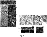
- copper traces produced from molecular inks A, B and C cannot be directly soldered.
- the solder dissolves in the copper trace and does not wet the surface of the copper traces. Resistance is 43-49 ⁇ and 13-17 ⁇ , respectively, for copper traces produced from molecular inks A and B.
- the solder wets the surface of the trace but does not adhere. Further, the resistance of the trace produced from molecular ink C is 200-250 ⁇ .
- the copper trace produced from molecular ink D can be directly soldered.
- the solder wets the surface of the trace and adheres well (D1 and D2), does not dissolve copper (D3), and forms a strong copper solder joint (D4).
- Fig. 2 further illustrates the morphology of the unsoldered copper traces depicted in Fig. 1 . It is evident from Fig. 2 that the copper trace produced from molecular ink D has a smooth and robust surface in comparison to the copper traces produced from the molecular inks A, B and C. Additionally, as evidenced in Fig. 3 , the soldered joint on copper trace produced from the molecular ink D is strong, exhibiting no breaks, no peel off and no flake off of the copper trace.
- Example 7 Other polymeric binders
- Comparative inks comprising copper nanoparticles (CuNP) and copper(II) formate anhydrate:3-diethylamino-1,2-propanediol (CuF:DEAPD) were formulated with other polymeric binders to assess performance of the comparative inks. It is apparent from the results illustrated below that selection of the polymeric binder is important for formulating an ink that can produce conductive copper traces having both direct solderabilty and longer term shelf stability, with increased conductivity and mechanical strength.
- Phenalloy TM 2870 (from DynaChem) is a phenol-formaldehyde resin in ethanol solution having a viscosity of 2000 cps and a solids content of 70%.
- a molecular ink was formulated in a similar manner as described above by mixing 0.4 wt% CuNP and 0.3 wt% of Phenalloy TM 2870 in CuF:DEAPD (1:1 mol eq Cu:DEAPD), and including 3 mol eq. water (H 2 O) (based on moles CuF:DEAPD) and 1.25 wt% glycerol as additional solvents.
- the ink was screen printed on to a film to produce ink traces of the same length (10 cm) and various nominal line widths as shown in Table 16.
- the ink traces were sintered at 110°C for 30 min, then 230°C for 5 min, then 250°C for 5 min (substrate temperature) under a nitrogen gas atmosphere containing 500 ppm oxygen gas.
- copper traces prepared using Phenalloy TM 2870 have similar conductivity to the traces produced from Rokrapol TM 7075.
- Poly(vinyl alcohol) was tested as a polymeric binder for ink formulations of the present invention. While the polymer was soluble in the amine diol (3-(diethylamino)-1-2-propanediol (DEAPD)), inclusion of copper formate hydrate in the mixture produced a precipitate. A corresponding copper ink formulated with 0.12 wt% of the polymer did not produce copper traces on a substrate when sintered.
- DEAPD diethylamino)-1-2-propanediol
- Poly(styrene sulfonic acid) was tested as a polymeric binder for ink formulations of the present invention.
- the polymer was found to be insoluble in the amine diol (3-(diethylamino)-1-2-propanediol (DEAPD) and insoluble in a mixture of copper formate hydrate and the amine diol.
- DEAPD diethylamino-1-2-propanediol
- a corresponding copper ink formulated with 0.12 wt% of the polymer did not produce copper traces on a substrate when sintered.
- Chitosan was tested as a polymeric binder for ink formulations of the present invention.
- the polymer was found to be insoluble in the amine diol (3-(diethylamino)-1-2-propanediol (DEAPD) and insoluble in a mixture of copper formate hydrate and the amine diol.
- DEAPD diethylamino-1-2-propanediol
- a corresponding copper ink formulated with 0.12 wt% of the polymer did not produce copper traces on a substrate when sintered.
- Poly(ethylene glycol) MN200 was tested as a polymeric binder for ink formulations of the present invention. While the polymer was soluble in the amine diol (3-(diethylamino)-1-2-propanediol (DEAPD) and a mixture of copper formate hydrate and the amine diol, a corresponding copper ink formulated with 0.12 wt% of the polymer only produced non-conducting copper traces with discontinuities on a substrate when sintered at 210-250°C.
- DEAPD diethylamino)-1-2-propanediol
- a silylated polyethylene glycol (PEG_silane) was tested as a polymeric binder for ink formulations of the present invention. While the polymer was soluble in the amine diol (3-(diethylamino)-1-2-propanediol (DEAPD) and a mixture of copper formate hydrate and the amine diol, a corresponding copper ink formulated with 0.12 wt% of the polymer only produced non-conducting copper traces with discontinuities on a substrate when sintered at 210-250°C.
- DEAPD diethylamino)-1-2-propanediol
- Poly(acrylic acid) sodium salt was tested as a polymeric binder for ink formulations of the present invention. While the polymer was soluble in the amine diol (3-(diethylamino)-1-2-propanediol (DEAPD) and a mixture of copper formate hydrate and the amine diol, a corresponding copper ink formulated with 0.12 wt% of the polymer only produced non-conducting copper traces with discontinuities on a substrate when sintered at 210-250°C. Furthermore, the copper traces showed poor adhesion to the substrate.
- DEAPD diethylamino)-1-2-propanediol
- a combination of poly(methacrylic acid) sodium salt and poly(vinyl butyral) was tested as a polymeric binder for ink formulations of the present invention.
- the polymers were soluble in the amine diol (3-(diethylamino)-1-2-propanediol (DEAPD) and a mixture of copper formate hydrate and the amine diol.
- DEAPD diethylamino-1-2-propanediol
- a corresponding copper ink formulated with 0.12 wt% of the polymer produced conducting copper traces, but the traces adhered poorly to the substrate.
- Lignin was tested as a polymeric binder for ink formulations of the present invention.
- the polymer was found to be insoluble in the amine diol (3-(diethylamino)-1-2-propanediol (DEAPD) and insoluble in a mixture of copper formate hydrate and the amine diol.
- DEAPD diethylamino-1-2-propanediol
- a corresponding copper ink formulated with 0.12 wt% of the polymer did not produce copper traces on a substrate when sintered.
- Polyaniline long chain grafted to lignin was tested as a polymeric binder for ink formulations of the present invention. While the polymer was soluble in the amine diol (3-(diethylamino)-1-2-propanediol (DEAPD)), inclusion of copper formate hydrate in the mixture produced a precipitate. A corresponding copper ink formulated with 0.12 wt% of the polymer did not produce copper traces on a substrate when sintered.
- DEAPD diethylamino)-1-2-propanediol
Landscapes
- Chemical & Material Sciences (AREA)
- Life Sciences & Earth Sciences (AREA)
- Organic Chemistry (AREA)
- Engineering & Computer Science (AREA)
- Wood Science & Technology (AREA)
- Materials Engineering (AREA)
- Chemical Kinetics & Catalysis (AREA)
- General Chemical & Material Sciences (AREA)
- Health & Medical Sciences (AREA)
- Thermal Sciences (AREA)
- Pest Control & Pesticides (AREA)
- Physics & Mathematics (AREA)
- General Health & Medical Sciences (AREA)
- Toxicology (AREA)
- Medicinal Chemistry (AREA)
- Polymers & Plastics (AREA)
- Inks, Pencil-Leads, Or Crayons (AREA)
- Conductive Materials (AREA)
- Powder Metallurgy (AREA)
- Manufacturing Of Printed Wiring (AREA)
- Non-Insulated Conductors (AREA)
- Parts Printed On Printed Circuit Boards (AREA)
- Manufacture Of Metal Powder And Suspensions Thereof (AREA)
Applications Claiming Priority (2)
| Application Number | Priority Date | Filing Date | Title |
|---|---|---|---|
| US201662367810P | 2016-07-28 | 2016-07-28 | |
| PCT/CA2017/050870 WO2018018136A1 (en) | 2016-07-28 | 2017-07-19 | Copper ink and conductive solderable copper traces produced therefrom |
Publications (3)
| Publication Number | Publication Date |
|---|---|
| EP3491082A1 EP3491082A1 (en) | 2019-06-05 |
| EP3491082A4 EP3491082A4 (en) | 2020-06-03 |
| EP3491082B1 true EP3491082B1 (en) | 2022-03-30 |
Family
ID=61015482
Family Applications (1)
| Application Number | Title | Priority Date | Filing Date |
|---|---|---|---|
| EP17833137.7A Active EP3491082B1 (en) | 2016-07-28 | 2017-07-19 | Copper ink and conductive solderable copper traces produced therefrom |
Country Status (8)
| Country | Link |
|---|---|
| US (1) | US10844238B2 (https=) |
| EP (1) | EP3491082B1 (https=) |
| JP (1) | JP6901549B2 (https=) |
| KR (1) | KR102360657B1 (https=) |
| CN (1) | CN109790409B (https=) |
| CA (1) | CA3032252C (https=) |
| TW (1) | TWI752986B (https=) |
| WO (1) | WO2018018136A1 (https=) |
Families Citing this family (12)
| Publication number | Priority date | Publication date | Assignee | Title |
|---|---|---|---|---|
| US11993719B2 (en) | 2017-10-27 | 2024-05-28 | National Research Council Of Canada | Boron nitride nanotube coated substrates for sintering of metallic traces by intense pulse light |
| CA3108631A1 (en) * | 2018-08-03 | 2020-02-06 | National Research Council Of Canada | Uv-sinterable molecular ink and processing thereof using broad spectrum uv light |
| TWI853828B (zh) * | 2018-08-07 | 2024-09-01 | 加拿大國家研究委員會 | 包覆成型的印刷電子零件和其製造方法 |
| CN112041500A (zh) * | 2018-10-11 | 2020-12-04 | 惠普发展公司,有限责任合伙企业 | 在织物中产生金属 |
| JP7269565B2 (ja) * | 2019-03-29 | 2023-05-09 | 学校法人 関西大学 | 導電性インキ組成物及び導電性積層体 |
| KR102213925B1 (ko) * | 2019-10-31 | 2021-02-08 | (주)쎄미시스코 | 실리카 입자를 포함하는 광소결용 잉크 조성물 |
| CN111269615A (zh) * | 2020-03-20 | 2020-06-12 | 辽宁大学 | 一种抗氧化无颗粒型铜导电墨水及其制备方法 |
| CN114799613B (zh) * | 2021-01-28 | 2023-11-07 | 深圳先进电子材料国际创新研究院 | 一种铜焊膏及其制备方法和应用 |
| CN114231092A (zh) * | 2021-12-15 | 2022-03-25 | 深圳先进技术研究院 | 一种铜导电油墨、柔性基底及柔性基底的制备方法 |
| CN114540889B (zh) * | 2022-03-25 | 2023-03-24 | 江阴纳力新材料科技有限公司 | 镀铜添加剂、镀铜液及其应用 |
| CN115171945A (zh) * | 2022-05-31 | 2022-10-11 | 宁波柔印电子科技有限责任公司 | 一种可用于大面积制备的铜浆及制作方法 |
| WO2025189292A1 (en) * | 2024-03-12 | 2025-09-18 | National Research Council Of Canada | System and method for lightning strike protection |
Family Cites Families (26)
| Publication number | Priority date | Publication date | Assignee | Title |
|---|---|---|---|---|
| DE2728465C2 (de) | 1977-06-24 | 1982-04-22 | Preh, Elektrofeinmechanische Werke, Jakob Preh, Nachf. Gmbh & Co, 8740 Bad Neustadt | Gedruckte Schaltung |
| US4396666A (en) | 1981-11-02 | 1983-08-02 | Cts Corporation | Solderable conductive employing an organic binder |
| US4687597A (en) | 1986-01-29 | 1987-08-18 | E. I. Du Pont De Nemours And Company | Copper conductor compositions |
| JPH01168867A (ja) * | 1987-12-24 | 1989-07-04 | Mitsubishi Gas Chem Co Inc | 銅膜形成物品の製造法 |
| JP2619289B2 (ja) | 1989-06-20 | 1997-06-11 | 三井金属鉱業株式会社 | 銅導電性組成物 |
| JP2660937B2 (ja) | 1990-07-16 | 1997-10-08 | 三井金属鉱業株式会社 | 銅導電性組成物 |
| US5882722A (en) | 1995-07-12 | 1999-03-16 | Partnerships Limited, Inc. | Electrical conductors formed from mixtures of metal powders and metallo-organic decompositions compounds |
| US20030148024A1 (en) | 2001-10-05 | 2003-08-07 | Kodas Toivo T. | Low viscosity precursor compositons and methods for the depositon of conductive electronic features |
| US7211205B2 (en) | 2003-01-29 | 2007-05-01 | Parelec, Inc. | High conductivity inks with improved adhesion |
| US7731812B2 (en) | 2004-10-19 | 2010-06-08 | E.I. Du Pont De Nemours And Company | Thick film conductor case compositions for LTCC tape |
| US8017044B2 (en) | 2008-07-08 | 2011-09-13 | Xerox Corporation | Bimodal metal nanoparticle ink and applications therefor |
| KR101276237B1 (ko) | 2010-12-02 | 2013-06-20 | 한국기계연구원 | 저온소결 전도성 금속막 및 이의 제조방법 |
| TWI532059B (zh) * | 2011-03-31 | 2016-05-01 | Taiyo Holdings Co Ltd | Conductive paste, conductive pattern formation method and conductive pattern |
| KR20120132424A (ko) | 2011-05-27 | 2012-12-05 | 한양대학교 산학협력단 | 전도성 구리 나노잉크의 광소결 방법 |
| JP5821551B2 (ja) * | 2011-11-10 | 2015-11-24 | 日立化成株式会社 | 導電粒子、異方導電材料及び導電接続構造体 |
| CN104284952A (zh) * | 2012-02-29 | 2015-01-14 | 耶路撒冷希伯来大学伊森姆研究发展有限公司 | 包含金属前体纳米颗粒的油墨 |
| CN103382327B (zh) * | 2012-05-02 | 2015-11-25 | 比亚迪股份有限公司 | 一种太阳能电池用铜墨及其制备方法、一种太阳能电池主栅的制造方法及太阳能电池组件 |
| KR20140044743A (ko) | 2012-10-04 | 2014-04-15 | 한양대학교 산학협력단 | 전도성 하이브리드 구리잉크 및 이를 이용한 광소결 방법 |
| KR101350507B1 (ko) | 2013-01-09 | 2014-01-17 | (주)쎄미시스코 | 금속 나노입자를 포함하는 전기전도성 잉크 및 이의 광 소결 방법 |
| JP2014182913A (ja) * | 2013-03-19 | 2014-09-29 | Fujifilm Corp | 導電膜形成用組成物およびこれを用いる導電膜の製造方法 |
| JP2014196427A (ja) * | 2013-03-29 | 2014-10-16 | 富士フイルム株式会社 | 導電膜形成用組成物およびこれを用いる導電膜の製造方法 |
| KR20150045605A (ko) | 2013-10-21 | 2015-04-29 | 전자부품연구원 | 구리 잉크 조성물 및 이를 이용한 도전 패턴 형성 방법 |
| KR101597651B1 (ko) | 2013-12-30 | 2016-02-25 | 전자부품연구원 | 고내열성을 갖는 나노산화구리 잉크 조성물 및 이를 이용한 전극 형성방법 |
| EP2918371A1 (en) | 2014-03-11 | 2015-09-16 | Heraeus Precious Metals North America Conshohocken LLC | Solderable conductive polymer thick film composition |
| KR20150134728A (ko) * | 2014-05-22 | 2015-12-02 | 주식회사 동진쎄미켐 | 전도성 조성물 |
| JP2016029638A (ja) * | 2014-07-15 | 2016-03-03 | 東洋インキScホールディングス株式会社 | レーザー加工用導電性ペースト |
-
2017
- 2017-07-19 KR KR1020197005617A patent/KR102360657B1/ko active Active
- 2017-07-19 WO PCT/CA2017/050870 patent/WO2018018136A1/en not_active Ceased
- 2017-07-19 JP JP2019504746A patent/JP6901549B2/ja active Active
- 2017-07-19 CA CA3032252A patent/CA3032252C/en active Active
- 2017-07-19 EP EP17833137.7A patent/EP3491082B1/en active Active
- 2017-07-19 US US16/321,076 patent/US10844238B2/en active Active
- 2017-07-19 CN CN201780059065.5A patent/CN109790409B/zh active Active
- 2017-07-26 TW TW106125020A patent/TWI752986B/zh active
Also Published As
| Publication number | Publication date |
|---|---|
| CN109790409A (zh) | 2019-05-21 |
| US10844238B2 (en) | 2020-11-24 |
| WO2018018136A1 (en) | 2018-02-01 |
| EP3491082A1 (en) | 2019-06-05 |
| CA3032252C (en) | 2025-07-08 |
| EP3491082A4 (en) | 2020-06-03 |
| CA3032252A1 (en) | 2018-02-01 |
| CN109790409B (zh) | 2022-03-04 |
| JP2019529599A (ja) | 2019-10-17 |
| JP6901549B2 (ja) | 2021-07-14 |
| KR102360657B1 (ko) | 2022-02-08 |
| US20190177565A1 (en) | 2019-06-13 |
| TWI752986B (zh) | 2022-01-21 |
| KR20190042586A (ko) | 2019-04-24 |
| TW201815994A (zh) | 2018-05-01 |
Similar Documents
| Publication | Publication Date | Title |
|---|---|---|
| EP3491082B1 (en) | Copper ink and conductive solderable copper traces produced therefrom | |
| TWI607114B (zh) | 導電膜的製造方法以及導電膜 | |
| JP4431543B2 (ja) | Ag−Pd合金ナノ粒子を用いる配線基板製造方法 | |
| TWI603342B (zh) | 導電膜形成用組成物及使用其的導電膜的製造方法 | |
| KR101782799B1 (ko) | 구리-아민 코-콤플렉스의 제조방법 및 이를 포함하는 전도성 이온 잉크 및 이를 이용한 미세 패턴전극의 제조방법 | |
| CN110809806A (zh) | 导电性糊料 | |
| EP3728492B1 (en) | Copper ink for high conductivity fine printing | |
| EP3335223B1 (en) | Photonic sintering of a polymer thick film copper conductor composition | |
| EP3662027B1 (en) | Copper ink | |
| JP2009196249A (ja) | 積層体および積層体の製造方法 | |
| HK40038080B (en) | Copper ink for high conductivity fine printing | |
| HK40038080A (en) | Copper ink for high conductivity fine printing | |
| TW201503163A (zh) | 導電膜形成用組成物及使用其的導電膜的製造方法 | |
| JP2015003970A (ja) | 導体パターン形成用インク |
Legal Events
| Date | Code | Title | Description |
|---|---|---|---|
| STAA | Information on the status of an ep patent application or granted ep patent |
Free format text: STATUS: THE INTERNATIONAL PUBLICATION HAS BEEN MADE |
|
| PUAI | Public reference made under article 153(3) epc to a published international application that has entered the european phase |
Free format text: ORIGINAL CODE: 0009012 |
|
| STAA | Information on the status of an ep patent application or granted ep patent |
Free format text: STATUS: REQUEST FOR EXAMINATION WAS MADE |
|
| 17P | Request for examination filed |
Effective date: 20190206 |
|
| AK | Designated contracting states |
Kind code of ref document: A1 Designated state(s): AL AT BE BG CH CY CZ DE DK EE ES FI FR GB GR HR HU IE IS IT LI LT LU LV MC MK MT NL NO PL PT RO RS SE SI SK SM TR |
|
| AX | Request for extension of the european patent |
Extension state: BA ME |
|
| DAV | Request for validation of the european patent (deleted) | ||
| DAX | Request for extension of the european patent (deleted) | ||
| A4 | Supplementary search report drawn up and despatched |
Effective date: 20200504 |
|
| RIC1 | Information provided on ipc code assigned before grant |
Ipc: C09D 11/52 20140101AFI20200424BHEP |
|
| REG | Reference to a national code |
Ref country code: DE Ref legal event code: R079 Ref document number: 602017055323 Country of ref document: DE Free format text: PREVIOUS MAIN CLASS: C09D0011520000 Ipc: C09D0011037000 |
|
| RIC1 | Information provided on ipc code assigned before grant |
Ipc: C09D 11/52 20140101ALI20210413BHEP Ipc: C09D 11/102 20140101ALI20210413BHEP Ipc: C09D 11/037 20140101AFI20210413BHEP |
|
| GRAP | Despatch of communication of intention to grant a patent |
Free format text: ORIGINAL CODE: EPIDOSNIGR1 |
|
| STAA | Information on the status of an ep patent application or granted ep patent |
Free format text: STATUS: GRANT OF PATENT IS INTENDED |
|
| INTG | Intention to grant announced |
Effective date: 20210618 |
|
| GRAJ | Information related to disapproval of communication of intention to grant by the applicant or resumption of examination proceedings by the epo deleted |
Free format text: ORIGINAL CODE: EPIDOSDIGR1 |
|
| STAA | Information on the status of an ep patent application or granted ep patent |
Free format text: STATUS: REQUEST FOR EXAMINATION WAS MADE |
|
| RIN1 | Information on inventor provided before grant (corrected) |
Inventor name: MALENFANT, PATRICK Inventor name: LIU, XIANG YANG Inventor name: PAQUET, CHANTAL Inventor name: DEORE, BHAVANA |
|
| INTC | Intention to grant announced (deleted) | ||
| GRAP | Despatch of communication of intention to grant a patent |
Free format text: ORIGINAL CODE: EPIDOSNIGR1 |
|
| STAA | Information on the status of an ep patent application or granted ep patent |
Free format text: STATUS: GRANT OF PATENT IS INTENDED |
|
| INTG | Intention to grant announced |
Effective date: 20211102 |
|
| GRAS | Grant fee paid |
Free format text: ORIGINAL CODE: EPIDOSNIGR3 |
|
| GRAA | (expected) grant |
Free format text: ORIGINAL CODE: 0009210 |
|
| STAA | Information on the status of an ep patent application or granted ep patent |
Free format text: STATUS: THE PATENT HAS BEEN GRANTED |
|
| AK | Designated contracting states |
Kind code of ref document: B1 Designated state(s): AL AT BE BG CH CY CZ DE DK EE ES FI FR GB GR HR HU IE IS IT LI LT LU LV MC MK MT NL NO PL PT RO RS SE SI SK SM TR |
|
| REG | Reference to a national code |
Ref country code: GB Ref legal event code: FG4D |
|
| REG | Reference to a national code |
Ref country code: CH Ref legal event code: EP |
|
| REG | Reference to a national code |
Ref country code: DE Ref legal event code: R096 Ref document number: 602017055323 Country of ref document: DE |
|
| REG | Reference to a national code |
Ref country code: AT Ref legal event code: REF Ref document number: 1479178 Country of ref document: AT Kind code of ref document: T Effective date: 20220415 |
|
| REG | Reference to a national code |
Ref country code: IE Ref legal event code: FG4D |
|
| REG | Reference to a national code |
Ref country code: SE Ref legal event code: TRGR |
|
| REG | Reference to a national code |
Ref country code: FI Ref legal event code: FGE |
|
| REG | Reference to a national code |
Ref country code: LT Ref legal event code: MG9D |
|
| PG25 | Lapsed in a contracting state [announced via postgrant information from national office to epo] |
Ref country code: RS Free format text: LAPSE BECAUSE OF FAILURE TO SUBMIT A TRANSLATION OF THE DESCRIPTION OR TO PAY THE FEE WITHIN THE PRESCRIBED TIME-LIMIT Effective date: 20220330 Ref country code: NO Free format text: LAPSE BECAUSE OF FAILURE TO SUBMIT A TRANSLATION OF THE DESCRIPTION OR TO PAY THE FEE WITHIN THE PRESCRIBED TIME-LIMIT Effective date: 20220630 Ref country code: LT Free format text: LAPSE BECAUSE OF FAILURE TO SUBMIT A TRANSLATION OF THE DESCRIPTION OR TO PAY THE FEE WITHIN THE PRESCRIBED TIME-LIMIT Effective date: 20220330 Ref country code: HR Free format text: LAPSE BECAUSE OF FAILURE TO SUBMIT A TRANSLATION OF THE DESCRIPTION OR TO PAY THE FEE WITHIN THE PRESCRIBED TIME-LIMIT Effective date: 20220330 Ref country code: BG Free format text: LAPSE BECAUSE OF FAILURE TO SUBMIT A TRANSLATION OF THE DESCRIPTION OR TO PAY THE FEE WITHIN THE PRESCRIBED TIME-LIMIT Effective date: 20220630 |
|
| REG | Reference to a national code |
Ref country code: NL Ref legal event code: MP Effective date: 20220330 |
|
| REG | Reference to a national code |
Ref country code: AT Ref legal event code: MK05 Ref document number: 1479178 Country of ref document: AT Kind code of ref document: T Effective date: 20220330 |
|
| PG25 | Lapsed in a contracting state [announced via postgrant information from national office to epo] |
Ref country code: LV Free format text: LAPSE BECAUSE OF FAILURE TO SUBMIT A TRANSLATION OF THE DESCRIPTION OR TO PAY THE FEE WITHIN THE PRESCRIBED TIME-LIMIT Effective date: 20220330 Ref country code: GR Free format text: LAPSE BECAUSE OF FAILURE TO SUBMIT A TRANSLATION OF THE DESCRIPTION OR TO PAY THE FEE WITHIN THE PRESCRIBED TIME-LIMIT Effective date: 20220701 |
|
| PG25 | Lapsed in a contracting state [announced via postgrant information from national office to epo] |
Ref country code: NL Free format text: LAPSE BECAUSE OF FAILURE TO SUBMIT A TRANSLATION OF THE DESCRIPTION OR TO PAY THE FEE WITHIN THE PRESCRIBED TIME-LIMIT Effective date: 20220330 |
|
| PG25 | Lapsed in a contracting state [announced via postgrant information from national office to epo] |
Ref country code: SM Free format text: LAPSE BECAUSE OF FAILURE TO SUBMIT A TRANSLATION OF THE DESCRIPTION OR TO PAY THE FEE WITHIN THE PRESCRIBED TIME-LIMIT Effective date: 20220330 Ref country code: SK Free format text: LAPSE BECAUSE OF FAILURE TO SUBMIT A TRANSLATION OF THE DESCRIPTION OR TO PAY THE FEE WITHIN THE PRESCRIBED TIME-LIMIT Effective date: 20220330 Ref country code: RO Free format text: LAPSE BECAUSE OF FAILURE TO SUBMIT A TRANSLATION OF THE DESCRIPTION OR TO PAY THE FEE WITHIN THE PRESCRIBED TIME-LIMIT Effective date: 20220330 Ref country code: PT Free format text: LAPSE BECAUSE OF FAILURE TO SUBMIT A TRANSLATION OF THE DESCRIPTION OR TO PAY THE FEE WITHIN THE PRESCRIBED TIME-LIMIT Effective date: 20220801 Ref country code: ES Free format text: LAPSE BECAUSE OF FAILURE TO SUBMIT A TRANSLATION OF THE DESCRIPTION OR TO PAY THE FEE WITHIN THE PRESCRIBED TIME-LIMIT Effective date: 20220330 Ref country code: EE Free format text: LAPSE BECAUSE OF FAILURE TO SUBMIT A TRANSLATION OF THE DESCRIPTION OR TO PAY THE FEE WITHIN THE PRESCRIBED TIME-LIMIT Effective date: 20220330 Ref country code: CZ Free format text: LAPSE BECAUSE OF FAILURE TO SUBMIT A TRANSLATION OF THE DESCRIPTION OR TO PAY THE FEE WITHIN THE PRESCRIBED TIME-LIMIT Effective date: 20220330 Ref country code: AT Free format text: LAPSE BECAUSE OF FAILURE TO SUBMIT A TRANSLATION OF THE DESCRIPTION OR TO PAY THE FEE WITHIN THE PRESCRIBED TIME-LIMIT Effective date: 20220330 |
|
| PG25 | Lapsed in a contracting state [announced via postgrant information from national office to epo] |
Ref country code: PL Free format text: LAPSE BECAUSE OF FAILURE TO SUBMIT A TRANSLATION OF THE DESCRIPTION OR TO PAY THE FEE WITHIN THE PRESCRIBED TIME-LIMIT Effective date: 20220330 Ref country code: IS Free format text: LAPSE BECAUSE OF FAILURE TO SUBMIT A TRANSLATION OF THE DESCRIPTION OR TO PAY THE FEE WITHIN THE PRESCRIBED TIME-LIMIT Effective date: 20220730 Ref country code: AL Free format text: LAPSE BECAUSE OF FAILURE TO SUBMIT A TRANSLATION OF THE DESCRIPTION OR TO PAY THE FEE WITHIN THE PRESCRIBED TIME-LIMIT Effective date: 20220330 |
|
| REG | Reference to a national code |
Ref country code: DE Ref legal event code: R097 Ref document number: 602017055323 Country of ref document: DE |
|
| PG25 | Lapsed in a contracting state [announced via postgrant information from national office to epo] |
Ref country code: DK Free format text: LAPSE BECAUSE OF FAILURE TO SUBMIT A TRANSLATION OF THE DESCRIPTION OR TO PAY THE FEE WITHIN THE PRESCRIBED TIME-LIMIT Effective date: 20220330 |
|
| PLBE | No opposition filed within time limit |
Free format text: ORIGINAL CODE: 0009261 |
|
| STAA | Information on the status of an ep patent application or granted ep patent |
Free format text: STATUS: NO OPPOSITION FILED WITHIN TIME LIMIT |
|
| PG25 | Lapsed in a contracting state [announced via postgrant information from national office to epo] |
Ref country code: MC Free format text: LAPSE BECAUSE OF FAILURE TO SUBMIT A TRANSLATION OF THE DESCRIPTION OR TO PAY THE FEE WITHIN THE PRESCRIBED TIME-LIMIT Effective date: 20220330 |
|
| REG | Reference to a national code |
Ref country code: CH Ref legal event code: PL |
|
| 26N | No opposition filed |
Effective date: 20230103 |
|
| REG | Reference to a national code |
Ref country code: BE Ref legal event code: MM Effective date: 20220731 |
|
| PG25 | Lapsed in a contracting state [announced via postgrant information from national office to epo] |
Ref country code: LU Free format text: LAPSE BECAUSE OF NON-PAYMENT OF DUE FEES Effective date: 20220719 Ref country code: LI Free format text: LAPSE BECAUSE OF NON-PAYMENT OF DUE FEES Effective date: 20220731 Ref country code: CH Free format text: LAPSE BECAUSE OF NON-PAYMENT OF DUE FEES Effective date: 20220731 |
|
| PG25 | Lapsed in a contracting state [announced via postgrant information from national office to epo] |
Ref country code: SI Free format text: LAPSE BECAUSE OF FAILURE TO SUBMIT A TRANSLATION OF THE DESCRIPTION OR TO PAY THE FEE WITHIN THE PRESCRIBED TIME-LIMIT Effective date: 20220330 Ref country code: BE Free format text: LAPSE BECAUSE OF NON-PAYMENT OF DUE FEES Effective date: 20220731 |
|
| P01 | Opt-out of the competence of the unified patent court (upc) registered |
Effective date: 20230523 |
|
| PG25 | Lapsed in a contracting state [announced via postgrant information from national office to epo] |
Ref country code: IE Free format text: LAPSE BECAUSE OF NON-PAYMENT OF DUE FEES Effective date: 20220719 |
|
| REG | Reference to a national code |
Ref country code: DE Ref legal event code: R081 Ref document number: 602017055323 Country of ref document: DE Owner name: NATIONAL RESEARCH COUNCIL OF CANADA, OTTAWA, CA Free format text: FORMER OWNER: NATIONAL RESEARCH COUNCIL OF CANADA, OTTAWA, ONTARIO, CA Ref country code: DE Ref legal event code: R081 Ref document number: 602017055323 Country of ref document: DE Owner name: E2IP TECHNOLOGIES INC., CA Free format text: FORMER OWNER: NATIONAL RESEARCH COUNCIL OF CANADA, OTTAWA, ONTARIO, CA |
|
| REG | Reference to a national code |
Ref country code: GB Ref legal event code: 732E Free format text: REGISTERED BETWEEN 20230720 AND 20230726 |
|
| REG | Reference to a national code |
Ref country code: FI Ref legal event code: PCE Owner name: E2IP TECHNOLOGIES INC. |
|
| PG25 | Lapsed in a contracting state [announced via postgrant information from national office to epo] |
Ref country code: HU Free format text: LAPSE BECAUSE OF FAILURE TO SUBMIT A TRANSLATION OF THE DESCRIPTION OR TO PAY THE FEE WITHIN THE PRESCRIBED TIME-LIMIT; INVALID AB INITIO Effective date: 20170719 |
|
| PG25 | Lapsed in a contracting state [announced via postgrant information from national office to epo] |
Ref country code: MK Free format text: LAPSE BECAUSE OF FAILURE TO SUBMIT A TRANSLATION OF THE DESCRIPTION OR TO PAY THE FEE WITHIN THE PRESCRIBED TIME-LIMIT Effective date: 20220330 Ref country code: CY Free format text: LAPSE BECAUSE OF FAILURE TO SUBMIT A TRANSLATION OF THE DESCRIPTION OR TO PAY THE FEE WITHIN THE PRESCRIBED TIME-LIMIT Effective date: 20220330 |
|
| PG25 | Lapsed in a contracting state [announced via postgrant information from national office to epo] |
Ref country code: TR Free format text: LAPSE BECAUSE OF FAILURE TO SUBMIT A TRANSLATION OF THE DESCRIPTION OR TO PAY THE FEE WITHIN THE PRESCRIBED TIME-LIMIT Effective date: 20220330 |
|
| PG25 | Lapsed in a contracting state [announced via postgrant information from national office to epo] |
Ref country code: MT Free format text: LAPSE BECAUSE OF FAILURE TO SUBMIT A TRANSLATION OF THE DESCRIPTION OR TO PAY THE FEE WITHIN THE PRESCRIBED TIME-LIMIT Effective date: 20220330 |
|
| PGFP | Annual fee paid to national office [announced via postgrant information from national office to epo] |
Ref country code: FI Payment date: 20250725 Year of fee payment: 9 |
|
| PGFP | Annual fee paid to national office [announced via postgrant information from national office to epo] |
Ref country code: DE Payment date: 20250722 Year of fee payment: 9 |
|
| PGFP | Annual fee paid to national office [announced via postgrant information from national office to epo] |
Ref country code: IT Payment date: 20250724 Year of fee payment: 9 |
|
| PGFP | Annual fee paid to national office [announced via postgrant information from national office to epo] |
Ref country code: GB Payment date: 20250722 Year of fee payment: 9 |
|
| PGFP | Annual fee paid to national office [announced via postgrant information from national office to epo] |
Ref country code: FR Payment date: 20250725 Year of fee payment: 9 |
|
| PGFP | Annual fee paid to national office [announced via postgrant information from national office to epo] |
Ref country code: SE Payment date: 20250722 Year of fee payment: 9 |