EP3335224B1 - Paste and process for forming a solderable polyimide based polymer thick film conductor - Google Patents
Paste and process for forming a solderable polyimide based polymer thick film conductor Download PDFInfo
- Publication number
- EP3335224B1 EP3335224B1 EP16751796.0A EP16751796A EP3335224B1 EP 3335224 B1 EP3335224 B1 EP 3335224B1 EP 16751796 A EP16751796 A EP 16751796A EP 3335224 B1 EP3335224 B1 EP 3335224B1
- Authority
- EP
- European Patent Office
- Prior art keywords
- polyimide
- bis
- thick film
- paste composition
- based polymer
- Prior art date
- Legal status (The legal status is an assumption and is not a legal conclusion. Google has not performed a legal analysis and makes no representation as to the accuracy of the status listed.)
- Active
Links
Images
Classifications
-
- B—PERFORMING OPERATIONS; TRANSPORTING
- B23—MACHINE TOOLS; METAL-WORKING NOT OTHERWISE PROVIDED FOR
- B23K—SOLDERING OR UNSOLDERING; WELDING; CLADDING OR PLATING BY SOLDERING OR WELDING; CUTTING BY APPLYING HEAT LOCALLY, e.g. FLAME CUTTING; WORKING BY LASER BEAM
- B23K35/00—Rods, electrodes, materials, or media, for use in soldering, welding, or cutting
- B23K35/22—Rods, electrodes, materials, or media, for use in soldering, welding, or cutting characterised by the composition or nature of the material
- B23K35/24—Selection of soldering or welding materials proper
- B23K35/30—Selection of soldering or welding materials proper with the principal constituent melting at less than 1550°C
- B23K35/3006—Ag as the principal constituent
-
- B—PERFORMING OPERATIONS; TRANSPORTING
- B23—MACHINE TOOLS; METAL-WORKING NOT OTHERWISE PROVIDED FOR
- B23K—SOLDERING OR UNSOLDERING; WELDING; CLADDING OR PLATING BY SOLDERING OR WELDING; CUTTING BY APPLYING HEAT LOCALLY, e.g. FLAME CUTTING; WORKING BY LASER BEAM
- B23K35/00—Rods, electrodes, materials, or media, for use in soldering, welding, or cutting
- B23K35/02—Rods, electrodes, materials, or media, for use in soldering, welding, or cutting characterised by mechanical features, e.g. shape
- B23K35/0222—Rods, electrodes, materials, or media, for use in soldering, welding, or cutting characterised by mechanical features, e.g. shape for use in soldering or brazing
- B23K35/0244—Powders, particles or spheres; Preforms made therefrom
- B23K35/025—Pastes, creams or slurries
-
- B—PERFORMING OPERATIONS; TRANSPORTING
- B23—MACHINE TOOLS; METAL-WORKING NOT OTHERWISE PROVIDED FOR
- B23K—SOLDERING OR UNSOLDERING; WELDING; CLADDING OR PLATING BY SOLDERING OR WELDING; CUTTING BY APPLYING HEAT LOCALLY, e.g. FLAME CUTTING; WORKING BY LASER BEAM
- B23K35/00—Rods, electrodes, materials, or media, for use in soldering, welding, or cutting
- B23K35/22—Rods, electrodes, materials, or media, for use in soldering, welding, or cutting characterised by the composition or nature of the material
- B23K35/36—Selection of non-metallic compositions, e.g. coatings or fluxes; Selection of soldering or welding materials, conjoint with selection of non-metallic compositions, both selections being of interest
- B23K35/3612—Selection of non-metallic compositions, e.g. coatings or fluxes; Selection of soldering or welding materials, conjoint with selection of non-metallic compositions, both selections being of interest with organic compounds as principal constituents
-
- B—PERFORMING OPERATIONS; TRANSPORTING
- B23—MACHINE TOOLS; METAL-WORKING NOT OTHERWISE PROVIDED FOR
- B23K—SOLDERING OR UNSOLDERING; WELDING; CLADDING OR PLATING BY SOLDERING OR WELDING; CUTTING BY APPLYING HEAT LOCALLY, e.g. FLAME CUTTING; WORKING BY LASER BEAM
- B23K35/00—Rods, electrodes, materials, or media, for use in soldering, welding, or cutting
- B23K35/22—Rods, electrodes, materials, or media, for use in soldering, welding, or cutting characterised by the composition or nature of the material
- B23K35/36—Selection of non-metallic compositions, e.g. coatings or fluxes; Selection of soldering or welding materials, conjoint with selection of non-metallic compositions, both selections being of interest
- B23K35/3612—Selection of non-metallic compositions, e.g. coatings or fluxes; Selection of soldering or welding materials, conjoint with selection of non-metallic compositions, both selections being of interest with organic compounds as principal constituents
- B23K35/3613—Polymers, e.g. resins
-
- C—CHEMISTRY; METALLURGY
- C09—DYES; PAINTS; POLISHES; NATURAL RESINS; ADHESIVES; COMPOSITIONS NOT OTHERWISE PROVIDED FOR; APPLICATIONS OF MATERIALS NOT OTHERWISE PROVIDED FOR
- C09D—COATING COMPOSITIONS, e.g. PAINTS, VARNISHES OR LACQUERS; FILLING PASTES; CHEMICAL PAINT OR INK REMOVERS; INKS; CORRECTING FLUIDS; WOODSTAINS; PASTES OR SOLIDS FOR COLOURING OR PRINTING; USE OF MATERIALS THEREFOR
- C09D5/00—Coating compositions, e.g. paints, varnishes or lacquers, characterised by their physical nature or the effects produced; Filling pastes
- C09D5/24—Electrically-conducting paints
-
- H—ELECTRICITY
- H01—ELECTRIC ELEMENTS
- H01B—CABLES; CONDUCTORS; INSULATORS; SELECTION OF MATERIALS FOR THEIR CONDUCTIVE, INSULATING OR DIELECTRIC PROPERTIES
- H01B1/00—Conductors or conductive bodies characterised by the conductive materials; Selection of materials as conductors
- H01B1/20—Conductive material dispersed in non-conductive organic material
- H01B1/22—Conductive material dispersed in non-conductive organic material the conductive material comprising metals or alloys
-
- H—ELECTRICITY
- H05—ELECTRIC TECHNIQUES NOT OTHERWISE PROVIDED FOR
- H05K—PRINTED CIRCUITS; CASINGS OR CONSTRUCTIONAL DETAILS OF ELECTRIC APPARATUS; MANUFACTURE OF ASSEMBLAGES OF ELECTRICAL COMPONENTS
- H05K1/00—Printed circuits
- H05K1/02—Details
- H05K1/09—Use of materials for the conductive, e.g. metallic pattern
- H05K1/092—Dispersed materials, e.g. conductive pastes or inks
- H05K1/095—Dispersed materials, e.g. conductive pastes or inks for polymer thick films, i.e. having a permanent organic polymeric binder
-
- H—ELECTRICITY
- H05—ELECTRIC TECHNIQUES NOT OTHERWISE PROVIDED FOR
- H05K—PRINTED CIRCUITS; CASINGS OR CONSTRUCTIONAL DETAILS OF ELECTRIC APPARATUS; MANUFACTURE OF ASSEMBLAGES OF ELECTRICAL COMPONENTS
- H05K2201/00—Indexing scheme relating to printed circuits covered by H05K1/00
- H05K2201/01—Dielectrics
- H05K2201/0137—Materials
- H05K2201/0154—Polyimide
-
- H—ELECTRICITY
- H05—ELECTRIC TECHNIQUES NOT OTHERWISE PROVIDED FOR
- H05K—PRINTED CIRCUITS; CASINGS OR CONSTRUCTIONAL DETAILS OF ELECTRIC APPARATUS; MANUFACTURE OF ASSEMBLAGES OF ELECTRICAL COMPONENTS
- H05K2201/00—Indexing scheme relating to printed circuits covered by H05K1/00
- H05K2201/02—Fillers; Particles; Fibers; Reinforcement materials
- H05K2201/0203—Fillers and particles
- H05K2201/0242—Shape of an individual particle
- H05K2201/0245—Flakes, flat particles or lamellar particles
Definitions
- the invention is directed to a paste composition for forming a solderable polyimide-based polymer thick film (PTF) conductor and a process for forming the conductor utilizing the paste
- a thick film composition comprises a functional phase that imparts appropriate electrically functional properties to the composition.
- the functional phase comprises electrically functional powders dispersed in an organic solvent containing a polymer.
- These compositions will typically contain a binder, e.g., a glass frit.
- a binder e.g., a glass frit.
- Such a composition is fired to burn out the polymer and solvent and to impart the electrically functional properties.
- the polymer remains as an integral part of the composition after drying and only the solvent is removed.
- a processing requirement may include a heat treatment such as curing as known to those skilled in the art of polymer thick film technology.
- PTF compositions are only stable up to approximately 200°C and therefore do not lend them to soldering as this is done at temperatures of 200 to 260°C. Further, many current PTF electrode compositions do not wet well with solder and do not possess good adhesion to the substrate after soldering.
- the invention provides a polyimide-based polymer thick film paste composition for forming a solderable polyimide-based polymer thick film conductor, the paste composition comprising:
- the polyimide polymer is represented by formula I: wherein X is C(CH 3 ) 2 , O, S(O) 2 , C(CF 3 ) 2 , O-Ph-C(CH 3 ) 2 -Ph-O, O-Ph-O- or a mixture of two or more of C(CH 3 ) 2 , O, S(O) 2 , C(CF 3 ) 2 , O-Ph-C(CH 3 ) 2 -Ph-O, O-Ph-O-; wherein Y is a diamine component or a mixture of diamine components selected from the group consisting of:m-phenylenediamine (MPD), 3,4'-diaminodiphenyl ether (3,4'-ODA), 4,4'-diamino-2,2'-bis(trifluoromethyl)biphenyl (TFMB), 3,3'-diaminodiphenyl sulfone (3,3'-DDS),
- the invention also provides an electrical device containing a solderable polyimide-based polymer thick film conductor formed from the paste composition of the invention.
- the invention further provides a process for forming a solderable polyimide-based polymer thick film conductor using the instant paste composition, comprising the steps of:
- the paste composition is fired at temperatures of from 320 to 380°C for at least 30 minutes. In another embodiment, the paste composition is fired at temperatures of from 320 to 380°C for at least 1 hour. In still another embodiment the paste composition is fired at temperatures of from 330 to 380°C for at least I hour and in other embodiments for 5 hours.
- step (iii) the paste composition applied in step (iii) is dried by heating at a temperature sufficient to remove the organic solvent.
- the invention also provides an electrical device containing a solderable polyimide-based polymer thick film conductor formed using the process of the invention.
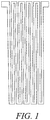
- Figure 1 illustrates the serpentine screen printed paste pattern used in the Comparative Experiment and the Examples.
- the invention relates to a paste composition for forming a solderable polyimide-based polymer thick film (PTF) conductor and a process for forming the conductor utilizing the paste.
- the paste is typically used In an electrical device to form an electrical conductor that is solderable has good adhesion and thereby provides for electrical connections.
- the main components of the instant polyimide-based polymer thick film paste composition are an electrically conductive metal powder, a polyimide polymer, an organosilicon compound and an organic solvent,
- the electrically conductive metal powder in the present polymer thick film composition is a powder of electrically conductive metal particles.
- the electrically conductive metal is selected from the group consisting of Ag, Cu, Au, Pd, Pt, Sn, Al, Ni and mixtures thereof
- the conductive particles may include silver (Ag).
- the conductive particles may, for example, include one or more of the following: Ag, Cu, Au, Pd, Pt, Sn, Al, Ni, Ag-Pd and Pt-Au.
- the conductive particles may include one or more of the following: (1) Al, Cu, Au, Ag, Pd and Pt; (2) an alloy of Al, Cu, Au, Ag, Pd and Pt; and (3) mixtures thereof.
- the conductive particles may include one of the above mentioned metals coated with another of the metals, e.g., Ag-coated Cu, Ag-coated-Ni. An embodiment may contain a mixture of any of the above.
- the metal when it is silver, it can be in the form of silver metal, alloys of silver or mixtures thereof.
- the silver can also be in the form of silver oxide (Ag 2 O), silver salts such as AgCl, AgNO 3 , AgOOCCH 3 (silver acetate), AgOOCF 3 (silver trifluoroacetate), silver orthophosphate (Ag 3 PO 4 ) or mixtures thereof.
- silver oxide Ag 2 O
- silver salts such as AgCl, AgNO 3 , AgOOCCH 3 (silver acetate), AgOOCF 3 (silver trifluoroacetate), silver orthophosphate (Ag 3 PO 4 ) or mixtures thereof.
- Other forms of silver compatible with the other thick-film paste components can also be used.
- the source of the electrically conductive metal can be in a flake form, a spherical form, a granular form, a crystalline form, other irregular forms and mixtures thereof.
- the concentration of the electrically conductive metal be as high as possible while maintaining other required characteristics of the paste composition that relate to either processing or final use.
- the electrically conductive metal is from 60 to 95 wt% of the polymer thick film paste composition. In a further embodiment, the source of the electrically conductive metal is from about 75 to about 90 wt% of the solid components of the thick film paste composition.
- the electrically conductive metal is silver and the silver is from 60 to 95 wt% of the polymer thick film paste composition. In another embodiment, the silver is from about 75 to about 90 wt% of the solid components of the thick film paste composition. As used herein, weight percent is written as wt%.
- the particle size of the electrically conductive metal is not subject to any particular limitation.
- the average particle size may be less than 10 microns, and, in a further embodiment, no more than 5 microns. In an aspect, the average particle size may be 0.1 to 5 microns, for example.
- particle size is intended to mean “average particle size”; “average particle size” means the 50% volume distribution size.
- the 50% volume distribution size can be denoted as D 50 .
- Volume distribution size may be determined by a number of methods understood by one of skill in the art, including but not limited to laser diffraction and dispersion method using a Microtrac particle size analyzer (Montgomeryville, PA). Laser light scattering, e.g., using a model LA-910 particle size analyzer available commercially from Horiba Instruments Inc. (Irvine, CA), may also be employed.
- a polyimide polymer that can withstand temperatures up to 320°C can be used in the paste composition used in the instant process.
- the polyimide polymer is represented by formula I: wherein X is C(CH 3 ) 2 , O, S(O) 2 , C(CF 3 ) 2 , O-Ph-C(CH 3 ) 2 -Ph-O, O-Ph-O- or a mixture of two or more of C(CH 3 ) 2 , O, S(O) 2 , C(CF 3 ) 2 , O-Ph-C(CH 3 ) 2 -Ph-O, O-Ph-O-; wherein Y is a diamine component or a mixture of diamine components selected from the group consisting of:m-phenylenediamine (MPD), 3,4'-diaminodiphenyl ether (3,4'-ODA), 4,4'-diamino-2,2'-bis(trifluoromethyl)biphenyl (TFMB), 3,3'-diaminodiphenyl sulfone (3,3'-DDS),
- the polyimide can be prepared in the dry and powdered state by reacting monomers 2,2'-Bis(trifluoromethyl)-4,4'-diamino biphenyl (TFMB), 2,2Bis(3-amino-4-hydroxyphenyl)hexafluoropropane (6F-AP) and Hexafluoroisopropylidenebis-phthalic dianhydride. (6-FDA).
- TFMB 2,2'-Bis(trifluoromethyl)-4,4'-diamino biphenyl
- 6F-AP 2,2Bis(3-amino-4-hydroxyphenyl)hexafluoropropane
- 6-FDA Hexafluoroisopropylidenebis-phthalic dianhydride
- the polyimide polymer is from 2 to 6 wt% of the polymer thick film paste composition.
- the ratio of the weight of the electrically conductive metal powder to the weight of the polyimide polymer is between 13 and 40.
- organosilicon compound is polydimethylsiloxane (PDMS).
- the electrically conductive metal powder is dispersed in and the polyimide polymer is dissolved in the organic solvent.
- the electrically conductive metal powder is dispersed by mechanical mixing to form a paste like composition having suitable consistency and rheology for printing.
- the solvent must be one which can dissolve the polyimide polymer and in which the electrically conductive metal powder is dispersible with an adequate degree of stability.
- the organic solvent is one that can be boiled off at relatively low temperature.
- the rheological properties of the solvent must be such that they lend good application properties to the composition. Such properties include dispersion of the electrically conductive metal powder with an adequate degree of stability, good application of composition, appropriate viscosity, thixotropy, appropriate wettability of the substrate and the electrically conductive metal powder and a good drying rate.
- Solvents suitable for use in the polyimide-based polymer thick film paste composition are acetates and terpenes such as alpha- or beta-terpineol or mixtures thereof with other solvents such as kerosene, dibutylphthalate, butyl carbitol, butyl carbitol acetate, hexylene glycol and high boiling alcohols and alcohol esters.
- solvents such as glycol ethers, ketones, esters and other solvents of like boiling points (in the range of 180°C to 250°C), and mixtures thereof may be used.
- the solvent is one or more components selected from the group consisting butyl carbitol acetate, dibasic acetates, diethyl adipate and triethylphosphate. Various combinations of these and other solvents are formulated to obtain the viscosity and volatility requirements desired. In addition, volatile liquids for promoting rapid hardening after application on the substrate may be included in the organic vehicle.
- screen-printing is expected to be a common method for the deposition of polymer thick film conductive compositions
- other conventional methods including stencil printing, syringe dispensing or other deposition or coating techniques may be utilized.
- the organic solvent is present up to 25 wt % of the total weight of the paste composition.
- the polymer thick film paste composition is deposited on a substrate typical of those used in electric devices.
- the substrate is impermeable to gases and moisture.
- the substrate can be a sheet of flexible material.
- the flexible material can be an impermeable material such as a polyimide film, e.g. Kapton®.
- the material can also be a polyester, e.g. polyethylene terephthalate, or a composite material made up of a combination of plastic sheet with optional metallic or dielectric layers deposited thereupon.
- the deposition of the polymer thick film conductive composition is performed preferably by screen printing, although other deposition techniques such as stencil printing, syringe dispensing or coating techniques can be utilized. In the case of screen-printing, the screen mesh size controls the thickness of deposited thick film.
- the deposited thick film conductive composition is dried, i.e., the solvent is evaporated, by exposure to heat, e.g. at 130°C for minutes.
- the paste is then cured by heating at a temperature of 320 to 380°C for at least 30 minutes to form the solderable polyimide-based polymer thick film conductor.
- the paste is cured by heating at a temperature of 330 to 380°C for at least 1 hour.
- the paste is cured by heating at a temperature of 330 to 380°C for at least 1 hour.
- the substrates used in the Examples were Kapton® 500HPP-ST and Kapton® 200RS100 films (obtained from the DuPont Co, Wilmington, DE) and used as received after cut into 2.5" x 3.5" pieces and alumina (AD-96) substrates (obtained from CoorsTek, Golden, CO) used with no further cleaning.
- the polyimide polymer used in the Comparative Experiments and the Examples was prepared as described above by reacting TFMB, 6F-AP and 6-FDA. in a ratio of 33/10/57.
- Adhesion was measured by a Scotch® Tape test in which the tape was applied to the cured sample and then pulled off. The adhesion was judged on a scale of from poor (>10% peeling) to good ( ⁇ 1% peeling).
- the SAC alloy with a composition of Sn96.5%Ag3.0%Cu0.5% was used for the solder wetting test. Either Alpha 611 or Kester 952 flux was used. In the solder wetting test the cured samples were typically dipped for 1 - 3 seconds into the SAC alloy pot that was kept at 225 - 250°C.
- a screen printable Ag composition was prepared using silver flakes having an average particle size of 3-4 micron.
- the components of the PTF silver conductor composition were: 84 wt % silver powder 3.4 wt% polyimide 5.3 wt% butylcarbitol acetate 2 wt% dibasic acetates (DBE-3) 5.3 wt% diethyl adipate wherein the wt% are based on the total weight of the composition.
- This composition contained no organosilicon compound.
- the components were combined and mixed for 30-60 seconds in a Thinky-type mixer, and then roll-milled.
- the composition was used to screen print a 600 square serpentine pattern (shown in Figure 1 ) on Kapton® 500HPP-ST. Using a 325 mesh stainless steel screen, several patterns were printed, and the silver paste was dried at 130°C for 10 min.
- the measured line resistance from the samples was 7.7 ⁇ .
- the average conductor thickness over the 600 square pattern was determined to be 12.7 ⁇ m using a profilometer. Therefore the resistivity was calculated to be 6.5 m ⁇ / ⁇ /mil.
- Some of the samples cured at 130°C for 10 min were cured further for 1 h at 300°C to give an average resistivity of 1.8 m ⁇ / ⁇ /mil.
- Solder wettability was tested in the manner described above using the parts cured at 130°C/300°C. The samples showed near 100% solder wetting, and adhesion found to be good. However, the samples cured at 130°C for 10 min were also cured further at 360°C for 5 h and showed a cohesive failure in adhesion.
- a screen printable Ag composition was prepared using silver flakes having an average particle size of 3-4 micron.
- the components of the PTF silver conductor composition were: 79.7 wt% silver powder 4 wt% polyimide 16.1 wt% triethylphosphate 0.2 wt% oleic acid wherein the wt% are based on the total weight of the composition.
- This composition contained no organosilicon compound.
- the components were combined and mixed for 30-60 seconds in a Thinky-type mixer, and then roll-milled.
- the composition was used to screen print a 600 square serpentine pattern (shown in Figure 1 ) on Kapton® 500HPP-ST. Using a 325 mesh stainless steel screen, several patterns were printed, and the silver paste was dried at 130°C for 10 min.
- the measured line resistance from the samples was 6.7 ⁇ .
- the average conductor thickness over the 600 square pattern was determined to be 13.8 ⁇ m using a profilometer. Therefore the resistivity was calculated to be 6.1 m ⁇ / ⁇ /mil.
- Some of the samples were cured further for 1 h at 300°C to give an average resistivity of 1.9 m ⁇ / ⁇ /mil.
- Solder wettability was tested in the manner described above using the parts cured at 130°C/300°C. The samples showed near 100% solder wetting, and adhesion found to be good. However, the samples cured at 130°C for 10 min were also cured further at 360°C for 5 h and showed a cohesive failure in adhesion.
- a screen printable Ag composition was prepared using silver flakes having an average particle size of 3-4 micron.
- the components of the PTF silver conductor composition were: 85.4 wt% silver powder 2.6 wt% polyimide 11.5 wt% triethylphosphate 0.5 wt% silicon oil (PDMS) wherein the wt% are based on the total weight of the composition.
- This composition contained 0.5 wt% organosilicon compound.
- the components were combined and mixed for 30-60 seconds in a Thinky-type mixer, and then roll-milled.
- the composition was used to screen print a 600 square serpentine pattern (shown in Figure 1 ) on Kapton® 500HPP-ST. Using a 200 mesh stainless steel screen, several patterns were printed, and the silver paste was dried at 130°C for 10 min, and then 300°C for 1 h. The average resistivity of 7.6 m ⁇ / ⁇ /mil was obtained. Solder wettability was tested in the manner described above using the samples. The samples showed less than 80% solder wetting, but no adhesion failure was observed.
- Some printed samples were also cured at 130°C for 10 min, and then cured further at 360°C for 5 h. Severe adhesive failure was observed and near 100% peeling was observed by the tape peel test.
- a screen printable Ag composition was prepared using silver flakes having an average particle size of 3-4 micron.
- the components of the PTF silver conductor composition were: 83.85 wt % silver powder 3.4 wt% polyimide 5.3 wt% butylcarbitol acetate 2.1 wt% dibasic acetates (DBE-3) 5.3 wt% diethyl adipate 0.05 wt% silicon oil wherein the wt% are based on the total weight of the composition.
- This composition contained 0.05 wt% organosilicon compound.
- the components were combined and mixed for 30-60 seconds in a Thinky-type mixer, and then roll-milled.
- the composition was used to screen print a 600 square serpentine pattern (shown in Figure 1 ) on Kapton® 500HPP-ST. Using a 325 mesh stainless steel screen, several patterns were printed, and the silver paste was dried at 130°C for 10 min and then at 200°C for 30 min.
- the measured line resistance from the samples was 4.53 ⁇ .
- the average conductor thickness over the 600 square pattern was determined to be 8.97 ⁇ m using a profilometer. Therefore the resistivity was calculated to be 2.7 m ⁇ / ⁇ /mil.
- a screen printable Ag composition was prepared using silver flakes having an average particle size of 3-4micron.
- the components of the PTF silver conductor composition were: 83.6 wt % silver powder 3.4 wt% polyimide 5.3 wt% butylcarbitol acetate 2 wt% dibasic acetates (DBE-3) 5.3 wt% diethyl adipate 0.4 wt% silicon oil (PDMS) wherein the wt% are based on the total weight of the composition.
- This composition contained 0.4 wt% organosilicon compound.
- the components were combined and mixed for 30-60 seconds in a Thinky-type mixer, and then roll-milled.
- the composition was used to screen print a 600 square serpentine pattern (shown in Figure 1 ) on Kapton® 500HPP-ST. Using a 325 mesh stainless steel screen, several patterns were printed, and the silver paste was dried at 130°C for 10 min, and then at 200°C for 30 min. The measured line resistance from the samples was 4.62 ⁇ .
- the samples were cured further for 5h at 360°C to give an average resistance of 3.43 ⁇ .
- the average conductor thickness over the 600 square pattern was determined to be 12.99 ⁇ m using a profilometer. Therefore the resistivity was calculated to be 3.0 m ⁇ / ⁇ /mil.
- Some of the samples were cured further for 5h at 360°C,however, adhesive failure was observed from some of the samples as cured.
- the tape peel test gave near 100% adhesive failure.
- a screen printable Ag composition was prepared using silver flakes having an average particle size of 3-4 micron.
- the components of the PTF silver conductor composition were: 83.4 wt % silver powder 3.4 wt% polyimide 5.3 wt% butylcarbitol acetate 2.2 wt% dibasic acetates (DBE-3) 5.4 wt% diethyl adipate 0.2 wt% silicon oil wherein the wt% are based on the total weight of the composition.
- the ratio of the weight of the silver powder to the weight of the polyimide polymer was 24.5. This composition contained 0.2 wt% organosilicon compound.
- the components were combined and mixed for 30-60 seconds in a Thinky-type mixer, and then roll-milled.
- the composition was used to screen print a 600 square serpentine pattern (shown in Figure 1 ) on Kapton® 500HPP-ST. Using a 200 mesh stainless steel screen, several patterns were printed, and the silver paste was dried at 130°C for 10 min and then cured at 300°C for 1h, which gave resistivity of 4.4 m ⁇ / ⁇ /mil.
- Solder wettability was also tested in the manner described above using the parts cured at 130°C/300°C. The samples showed 100% solder wetting. Adhesion was tested for the samples and was found to be good.
- Some of the printed samples were also cured at 130°C for 10 min , and then additionally for 5 h at 360°C to give an average resistivity of 3.2 m ⁇ / ⁇ /mil. No adhesion failure was observed. The samples showed near 100% solder wetting.
- a screen printable Ag composition was prepared using silver flakes having an average particle size of 3-4 micron.
- the components of the PTF silver conductor composition were: 79.1 wt% silver powder 4 wt% polyimide 16.5 wt% triethylphosphate 0.2 wt% oleic acid 0.2 wt% silicon oil (PDMS) wherein the wt% are based on the total weight of the composition.
- the ratio of the weight of the silver powder to the weight of the polyimide polymer was 19.8.
- This composition contained 0.2 wt% organosilicon compound.
- the components were combined and mixed for 30-60 seconds in a Thinky-type mixer, and then roll-milled.
- the composition was used to screen print a 600 square serpentine pattern (shown in Figure 1 ) on Kapton® 500HPP-ST. Using a 200 mesh stainless steel screen, several patterns were printed, and the silver paste was cured at 130°C for 10 min, and then 300°C for 1h to give an average resistivity of 3.9 m ⁇ / ⁇ /mil.
- Solder wettability was tested in the manner described above using the samples. The samples showed near 100% solder wetting. Adhesion was tested for the samples and was found to be good.
- a screen printable Ag composition was prepared using silver flakes having an average particle size of 3-4 micron.
- the components of the PTF silver conductor composition were: 85.7 wt% silver powder 2.6 wt% polyimide 11.4 wt% triethylphosphate 0.3 wt% silicon oil (PDMS) wherein the wt% are based on the total weight of the composition.
- the ratio of the weight of the silver powder to the weight of the polyimide polymer was 33.
- This composition contained 0.3 wt% organosilicon compound.
- the components were combined and mixed for 30-60 seconds in a Thinky-type mixer, and then roll-milled.
- the composition was used to screen print a 600 square serpentine pattern (shown in Figure 1 ) on Kapton® 500HPP-ST. Using a 325 mesh stainless steel screen, several patterns were printed, and the silver paste was cured at 130°C for 10 min, and then 300°C for 1h to give an average resistivity of 5.3 m ⁇ / ⁇ /mil. Solder wettability was tested in the manner described above using the samples. The samples showed nearly 100% solder wetting. No adhesion failure was observed by the tape peel test.
Landscapes
- Engineering & Computer Science (AREA)
- Mechanical Engineering (AREA)
- Chemical & Material Sciences (AREA)
- Dispersion Chemistry (AREA)
- Microelectronics & Electronic Packaging (AREA)
- Physics & Mathematics (AREA)
- Spectroscopy & Molecular Physics (AREA)
- Life Sciences & Earth Sciences (AREA)
- Materials Engineering (AREA)
- Wood Science & Technology (AREA)
- Organic Chemistry (AREA)
- Conductive Materials (AREA)
- Compositions Of Macromolecular Compounds (AREA)
- Macromolecular Compounds Obtained By Forming Nitrogen-Containing Linkages In General (AREA)
- Parts Printed On Printed Circuit Boards (AREA)
Applications Claiming Priority (2)
| Application Number | Priority Date | Filing Date | Title |
|---|---|---|---|
| US14/824,202 US9649730B2 (en) | 2015-08-12 | 2015-08-12 | Paste and process for forming a solderable polyimide-based polymer thick film conductor |
| PCT/US2016/045997 WO2017027456A1 (en) | 2015-08-12 | 2016-08-08 | Paste and process for forming a solderable polyimide–based polymer thick film conductor |
Publications (2)
| Publication Number | Publication Date |
|---|---|
| EP3335224A1 EP3335224A1 (en) | 2018-06-20 |
| EP3335224B1 true EP3335224B1 (en) | 2019-06-12 |
Family
ID=56686979
Family Applications (1)
| Application Number | Title | Priority Date | Filing Date |
|---|---|---|---|
| EP16751796.0A Active EP3335224B1 (en) | 2015-08-12 | 2016-08-08 | Paste and process for forming a solderable polyimide based polymer thick film conductor |
Country Status (5)
| Country | Link |
|---|---|
| US (1) | US9649730B2 (https=) |
| EP (1) | EP3335224B1 (https=) |
| JP (1) | JP6737874B2 (https=) |
| CN (1) | CN108140446B (https=) |
| WO (1) | WO2017027456A1 (https=) |
Families Citing this family (3)
| Publication number | Priority date | Publication date | Assignee | Title |
|---|---|---|---|---|
| US20170044382A1 (en) * | 2015-08-12 | 2017-02-16 | E I Du Pont De Nemours And Company | Process for forming a solderable polyimide-based polymer thick film conductor |
| CN109776826B (zh) * | 2019-01-21 | 2020-09-29 | 深圳丹邦科技股份有限公司 | 一种聚酰亚胺厚膜和量子碳基膜、及其制备方法 |
| CN121373898B (zh) * | 2025-12-23 | 2026-03-10 | 深圳市同方电子新材料有限公司 | 一种易分散锡粉及其制备方法和锡膏 |
Family Cites Families (21)
| Publication number | Priority date | Publication date | Assignee | Title |
|---|---|---|---|---|
| JPS60149673A (ja) * | 1983-09-30 | 1985-08-07 | エレクトロ マテリアルズ コ−ポレ−シヨン オブ アメリカ | 導電性皮膜の形成方法 |
| JPS6183250A (ja) * | 1984-09-29 | 1986-04-26 | Nitto Electric Ind Co Ltd | 電子部品用導電性ペ−スト組成物 |
| JPH0565456A (ja) * | 1991-09-09 | 1993-03-19 | Sumitomo Bakelite Co Ltd | 気密封止用樹脂ペースト |
| US5545429A (en) * | 1994-07-01 | 1996-08-13 | International Business Machines Corporation | Fabrication of double side fully metallized plated thru-holes, in polymer structures, without seeding or photoprocess |
| US6344157B1 (en) * | 1999-02-12 | 2002-02-05 | National Starch And Chemical Investment Holding Corporation | Conductive and resistive materials with electrical stability for use in electronics devices |
| JP2003129017A (ja) * | 2001-10-25 | 2003-05-08 | Sumitomo Bakelite Co Ltd | 導電性接着フィルム及びこれを用いた半導体装置 |
| US7348373B2 (en) * | 2004-01-09 | 2008-03-25 | E.I. Du Pont De Nemours And Company | Polyimide compositions having resistance to water sorption, and methods relating thereto |
| US7169330B2 (en) | 2004-02-25 | 2007-01-30 | E. I. Du Pont De Nemours And Company | Composition of conductive paste |
| CN1835129B (zh) * | 2005-03-16 | 2010-04-28 | E.I.内穆尔杜邦公司 | 导电性浆状组合物 |
| US7745516B2 (en) | 2005-10-12 | 2010-06-29 | E. I. Du Pont De Nemours And Company | Composition of polyimide and sterically-hindered hydrophobic epoxy |
| JP2008106145A (ja) * | 2006-10-25 | 2008-05-08 | Sekisui Chem Co Ltd | 焼結性導電ペースト |
| US8270145B2 (en) | 2007-12-04 | 2012-09-18 | Cda Processing Limited Liability Company | Screen-printable encapsulants based on soluble polybenzoxazoles |
| CN102169739B (zh) * | 2011-02-25 | 2012-09-05 | 乐山新天源太阳能电力有限公司 | 太阳电池用纳米铝浆及其制备方法 |
| JP6028727B2 (ja) * | 2011-05-18 | 2016-11-16 | 戸田工業株式会社 | 銅粉末、銅ペースト、導電性塗膜の製造方法及び導電性塗膜 |
| TW201339279A (zh) * | 2011-11-24 | 2013-10-01 | Showa Denko Kk | 導電圖型形成方法及藉由光照射或微波加熱的導電圖型形成用組成物 |
| JP5321723B1 (ja) * | 2012-10-29 | 2013-10-23 | 横浜ゴム株式会社 | 導電性組成物および太陽電池セル |
| US9818718B2 (en) * | 2012-10-30 | 2017-11-14 | Kaken Tech Co., Ltd. | Conductive paste and die bonding method |
| JP5700864B2 (ja) * | 2013-05-15 | 2015-04-15 | 石原ケミカル株式会社 | 銅微粒子分散液、導電膜形成方法及び回路基板 |
| US9190188B2 (en) * | 2013-06-13 | 2015-11-17 | E I Du Pont De Nemours And Company | Photonic sintering of polymer thick film copper conductor compositions |
| JP2015032493A (ja) * | 2013-08-05 | 2015-02-16 | 富士フイルム株式会社 | 導電膜形成用組成物およびそれを用いる導電膜の製造方法 |
| CN104650653B (zh) * | 2013-11-22 | 2017-09-01 | 苏州冷石纳米材料科技有限公司 | 一种纳米导电银浆及其制备方法 |
-
2015
- 2015-08-12 US US14/824,202 patent/US9649730B2/en active Active
-
2016
- 2016-08-08 EP EP16751796.0A patent/EP3335224B1/en active Active
- 2016-08-08 JP JP2018507563A patent/JP6737874B2/ja active Active
- 2016-08-08 CN CN201680058560.XA patent/CN108140446B/zh active Active
- 2016-08-08 WO PCT/US2016/045997 patent/WO2017027456A1/en not_active Ceased
Non-Patent Citations (1)
| Title |
|---|
| None * |
Also Published As
| Publication number | Publication date |
|---|---|
| CN108140446A (zh) | 2018-06-08 |
| CN108140446B (zh) | 2020-07-31 |
| JP6737874B2 (ja) | 2020-08-12 |
| US9649730B2 (en) | 2017-05-16 |
| EP3335224A1 (en) | 2018-06-20 |
| JP2018529802A (ja) | 2018-10-11 |
| WO2017027456A1 (en) | 2017-02-16 |
| US20170043435A1 (en) | 2017-02-16 |
Similar Documents
| Publication | Publication Date | Title |
|---|---|---|
| JP7168701B2 (ja) | ポリイミド系ポリマー厚膜組成物 | |
| JPWO2017033911A1 (ja) | 低温焼結性に優れる金属ペースト及び該金属ペーストの製造方法 | |
| EP1943311A1 (en) | Compositions comprising polyimide and hydrophobic epoxy, and methods relating thereto | |
| EP3335224B1 (en) | Paste and process for forming a solderable polyimide based polymer thick film conductor | |
| US20170200539A1 (en) | Polyimide-based polymer thick film resistor composition | |
| EP3335223B1 (en) | Photonic sintering of a polymer thick film copper conductor composition | |
| JP5881613B2 (ja) | 導電性組成物、及び導電膜の形成方法 | |
| JP2018529802A5 (https=) | ||
| EP3335226B1 (en) | Photonic sintering of a solderable polymer thick film copper conductor composition | |
| US20160183328A1 (en) | Method and devices for high temperature thick film pastes | |
| JP6737872B2 (ja) | はんだ付け可能なポリイミド系ポリマー厚膜導電体を形成するためのプロセス | |
| US10508217B2 (en) | Polyimide-based polymer thick film resistor composition | |
| JP3917037B2 (ja) | 外部電極及びそれを備えた電子部品 | |
| JP5654463B2 (ja) | 金属および乳酸縮合物から構成される物質および電子部品 | |
| JP2018525494A5 (https=) | ||
| WO2019031323A1 (ja) | 金属インク |
Legal Events
| Date | Code | Title | Description |
|---|---|---|---|
| STAA | Information on the status of an ep patent application or granted ep patent |
Free format text: STATUS: THE INTERNATIONAL PUBLICATION HAS BEEN MADE |
|
| PUAI | Public reference made under article 153(3) epc to a published international application that has entered the european phase |
Free format text: ORIGINAL CODE: 0009012 |
|
| STAA | Information on the status of an ep patent application or granted ep patent |
Free format text: STATUS: REQUEST FOR EXAMINATION WAS MADE |
|
| 17P | Request for examination filed |
Effective date: 20180201 |
|
| AK | Designated contracting states |
Kind code of ref document: A1 Designated state(s): AL AT BE BG CH CY CZ DE DK EE ES FI FR GB GR HR HU IE IS IT LI LT LU LV MC MK MT NL NO PL PT RO RS SE SI SK SM TR |
|
| AX | Request for extension of the european patent |
Extension state: BA ME |
|
| DAV | Request for validation of the european patent (deleted) | ||
| DAX | Request for extension of the european patent (deleted) | ||
| GRAP | Despatch of communication of intention to grant a patent |
Free format text: ORIGINAL CODE: EPIDOSNIGR1 |
|
| STAA | Information on the status of an ep patent application or granted ep patent |
Free format text: STATUS: GRANT OF PATENT IS INTENDED |
|
| RIC1 | Information provided on ipc code assigned before grant |
Ipc: H05K 1/09 20060101ALI20181116BHEP Ipc: H01B 1/22 20060101AFI20181116BHEP Ipc: B23K 35/22 20060101ALI20181116BHEP |
|
| INTG | Intention to grant announced |
Effective date: 20181221 |
|
| GRAS | Grant fee paid |
Free format text: ORIGINAL CODE: EPIDOSNIGR3 |
|
| GRAA | (expected) grant |
Free format text: ORIGINAL CODE: 0009210 |
|
| STAA | Information on the status of an ep patent application or granted ep patent |
Free format text: STATUS: THE PATENT HAS BEEN GRANTED |
|
| AK | Designated contracting states |
Kind code of ref document: B1 Designated state(s): AL AT BE BG CH CY CZ DE DK EE ES FI FR GB GR HR HU IE IS IT LI LT LU LV MC MK MT NL NO PL PT RO RS SE SI SK SM TR |
|
| REG | Reference to a national code |
Ref country code: GB Ref legal event code: FG4D |
|
| REG | Reference to a national code |
Ref country code: CH Ref legal event code: EP |
|
| REG | Reference to a national code |
Ref country code: AT Ref legal event code: REF Ref document number: 1143635 Country of ref document: AT Kind code of ref document: T Effective date: 20190615 |
|
| REG | Reference to a national code |
Ref country code: DE Ref legal event code: R096 Ref document number: 602016015284 Country of ref document: DE |
|
| REG | Reference to a national code |
Ref country code: IE Ref legal event code: FG4D |
|
| REG | Reference to a national code |
Ref country code: NL Ref legal event code: MP Effective date: 20190612 |
|
| REG | Reference to a national code |
Ref country code: LT Ref legal event code: MG4D |
|
| PG25 | Lapsed in a contracting state [announced via postgrant information from national office to epo] |
Ref country code: FI Free format text: LAPSE BECAUSE OF FAILURE TO SUBMIT A TRANSLATION OF THE DESCRIPTION OR TO PAY THE FEE WITHIN THE PRESCRIBED TIME-LIMIT Effective date: 20190612 Ref country code: LT Free format text: LAPSE BECAUSE OF FAILURE TO SUBMIT A TRANSLATION OF THE DESCRIPTION OR TO PAY THE FEE WITHIN THE PRESCRIBED TIME-LIMIT Effective date: 20190612 Ref country code: AL Free format text: LAPSE BECAUSE OF FAILURE TO SUBMIT A TRANSLATION OF THE DESCRIPTION OR TO PAY THE FEE WITHIN THE PRESCRIBED TIME-LIMIT Effective date: 20190612 Ref country code: SE Free format text: LAPSE BECAUSE OF FAILURE TO SUBMIT A TRANSLATION OF THE DESCRIPTION OR TO PAY THE FEE WITHIN THE PRESCRIBED TIME-LIMIT Effective date: 20190612 Ref country code: HR Free format text: LAPSE BECAUSE OF FAILURE TO SUBMIT A TRANSLATION OF THE DESCRIPTION OR TO PAY THE FEE WITHIN THE PRESCRIBED TIME-LIMIT Effective date: 20190612 Ref country code: NO Free format text: LAPSE BECAUSE OF FAILURE TO SUBMIT A TRANSLATION OF THE DESCRIPTION OR TO PAY THE FEE WITHIN THE PRESCRIBED TIME-LIMIT Effective date: 20190912 |
|
| PG25 | Lapsed in a contracting state [announced via postgrant information from national office to epo] |
Ref country code: GR Free format text: LAPSE BECAUSE OF FAILURE TO SUBMIT A TRANSLATION OF THE DESCRIPTION OR TO PAY THE FEE WITHIN THE PRESCRIBED TIME-LIMIT Effective date: 20190913 Ref country code: LV Free format text: LAPSE BECAUSE OF FAILURE TO SUBMIT A TRANSLATION OF THE DESCRIPTION OR TO PAY THE FEE WITHIN THE PRESCRIBED TIME-LIMIT Effective date: 20190612 Ref country code: RS Free format text: LAPSE BECAUSE OF FAILURE TO SUBMIT A TRANSLATION OF THE DESCRIPTION OR TO PAY THE FEE WITHIN THE PRESCRIBED TIME-LIMIT Effective date: 20190612 Ref country code: BG Free format text: LAPSE BECAUSE OF FAILURE TO SUBMIT A TRANSLATION OF THE DESCRIPTION OR TO PAY THE FEE WITHIN THE PRESCRIBED TIME-LIMIT Effective date: 20190912 |
|
| REG | Reference to a national code |
Ref country code: AT Ref legal event code: MK05 Ref document number: 1143635 Country of ref document: AT Kind code of ref document: T Effective date: 20190612 |
|
| PG25 | Lapsed in a contracting state [announced via postgrant information from national office to epo] |
Ref country code: SK Free format text: LAPSE BECAUSE OF FAILURE TO SUBMIT A TRANSLATION OF THE DESCRIPTION OR TO PAY THE FEE WITHIN THE PRESCRIBED TIME-LIMIT Effective date: 20190612 Ref country code: EE Free format text: LAPSE BECAUSE OF FAILURE TO SUBMIT A TRANSLATION OF THE DESCRIPTION OR TO PAY THE FEE WITHIN THE PRESCRIBED TIME-LIMIT Effective date: 20190612 Ref country code: CZ Free format text: LAPSE BECAUSE OF FAILURE TO SUBMIT A TRANSLATION OF THE DESCRIPTION OR TO PAY THE FEE WITHIN THE PRESCRIBED TIME-LIMIT Effective date: 20190612 Ref country code: NL Free format text: LAPSE BECAUSE OF FAILURE TO SUBMIT A TRANSLATION OF THE DESCRIPTION OR TO PAY THE FEE WITHIN THE PRESCRIBED TIME-LIMIT Effective date: 20190612 Ref country code: RO Free format text: LAPSE BECAUSE OF FAILURE TO SUBMIT A TRANSLATION OF THE DESCRIPTION OR TO PAY THE FEE WITHIN THE PRESCRIBED TIME-LIMIT Effective date: 20190612 Ref country code: PT Free format text: LAPSE BECAUSE OF FAILURE TO SUBMIT A TRANSLATION OF THE DESCRIPTION OR TO PAY THE FEE WITHIN THE PRESCRIBED TIME-LIMIT Effective date: 20191014 Ref country code: AT Free format text: LAPSE BECAUSE OF FAILURE TO SUBMIT A TRANSLATION OF THE DESCRIPTION OR TO PAY THE FEE WITHIN THE PRESCRIBED TIME-LIMIT Effective date: 20190612 |
|
| PG25 | Lapsed in a contracting state [announced via postgrant information from national office to epo] |
Ref country code: SM Free format text: LAPSE BECAUSE OF FAILURE TO SUBMIT A TRANSLATION OF THE DESCRIPTION OR TO PAY THE FEE WITHIN THE PRESCRIBED TIME-LIMIT Effective date: 20190612 Ref country code: IT Free format text: LAPSE BECAUSE OF FAILURE TO SUBMIT A TRANSLATION OF THE DESCRIPTION OR TO PAY THE FEE WITHIN THE PRESCRIBED TIME-LIMIT Effective date: 20190612 Ref country code: IS Free format text: LAPSE BECAUSE OF FAILURE TO SUBMIT A TRANSLATION OF THE DESCRIPTION OR TO PAY THE FEE WITHIN THE PRESCRIBED TIME-LIMIT Effective date: 20191012 Ref country code: ES Free format text: LAPSE BECAUSE OF FAILURE TO SUBMIT A TRANSLATION OF THE DESCRIPTION OR TO PAY THE FEE WITHIN THE PRESCRIBED TIME-LIMIT Effective date: 20190612 |
|
| REG | Reference to a national code |
Ref country code: DE Ref legal event code: R097 Ref document number: 602016015284 Country of ref document: DE |
|
| PG25 | Lapsed in a contracting state [announced via postgrant information from national office to epo] |
Ref country code: TR Free format text: LAPSE BECAUSE OF FAILURE TO SUBMIT A TRANSLATION OF THE DESCRIPTION OR TO PAY THE FEE WITHIN THE PRESCRIBED TIME-LIMIT Effective date: 20190612 |
|
| PLBE | No opposition filed within time limit |
Free format text: ORIGINAL CODE: 0009261 |
|
| STAA | Information on the status of an ep patent application or granted ep patent |
Free format text: STATUS: NO OPPOSITION FILED WITHIN TIME LIMIT |
|
| PG25 | Lapsed in a contracting state [announced via postgrant information from national office to epo] |
Ref country code: DK Free format text: LAPSE BECAUSE OF FAILURE TO SUBMIT A TRANSLATION OF THE DESCRIPTION OR TO PAY THE FEE WITHIN THE PRESCRIBED TIME-LIMIT Effective date: 20190612 Ref country code: PL Free format text: LAPSE BECAUSE OF FAILURE TO SUBMIT A TRANSLATION OF THE DESCRIPTION OR TO PAY THE FEE WITHIN THE PRESCRIBED TIME-LIMIT Effective date: 20190612 |
|
| 26N | No opposition filed |
Effective date: 20200313 |
|
| PG25 | Lapsed in a contracting state [announced via postgrant information from national office to epo] |
Ref country code: LI Free format text: LAPSE BECAUSE OF NON-PAYMENT OF DUE FEES Effective date: 20190831 Ref country code: CH Free format text: LAPSE BECAUSE OF NON-PAYMENT OF DUE FEES Effective date: 20190831 Ref country code: LU Free format text: LAPSE BECAUSE OF NON-PAYMENT OF DUE FEES Effective date: 20190808 Ref country code: MC Free format text: LAPSE BECAUSE OF FAILURE TO SUBMIT A TRANSLATION OF THE DESCRIPTION OR TO PAY THE FEE WITHIN THE PRESCRIBED TIME-LIMIT Effective date: 20190612 Ref country code: SI Free format text: LAPSE BECAUSE OF FAILURE TO SUBMIT A TRANSLATION OF THE DESCRIPTION OR TO PAY THE FEE WITHIN THE PRESCRIBED TIME-LIMIT Effective date: 20190612 Ref country code: IS Free format text: LAPSE BECAUSE OF FAILURE TO SUBMIT A TRANSLATION OF THE DESCRIPTION OR TO PAY THE FEE WITHIN THE PRESCRIBED TIME-LIMIT Effective date: 20200224 |
|
| REG | Reference to a national code |
Ref country code: BE Ref legal event code: MM Effective date: 20190831 |
|
| PG2D | Information on lapse in contracting state deleted |
Ref country code: IS |
|
| PG25 | Lapsed in a contracting state [announced via postgrant information from national office to epo] |
Ref country code: IE Free format text: LAPSE BECAUSE OF NON-PAYMENT OF DUE FEES Effective date: 20190808 Ref country code: FR Free format text: LAPSE BECAUSE OF NON-PAYMENT OF DUE FEES Effective date: 20190812 |
|
| PG25 | Lapsed in a contracting state [announced via postgrant information from national office to epo] |
Ref country code: BE Free format text: LAPSE BECAUSE OF NON-PAYMENT OF DUE FEES Effective date: 20190831 |
|
| GBPC | Gb: european patent ceased through non-payment of renewal fee |
Effective date: 20200808 |
|
| PG25 | Lapsed in a contracting state [announced via postgrant information from national office to epo] |
Ref country code: CY Free format text: LAPSE BECAUSE OF FAILURE TO SUBMIT A TRANSLATION OF THE DESCRIPTION OR TO PAY THE FEE WITHIN THE PRESCRIBED TIME-LIMIT Effective date: 20190612 |
|
| PG25 | Lapsed in a contracting state [announced via postgrant information from national office to epo] |
Ref country code: MT Free format text: LAPSE BECAUSE OF FAILURE TO SUBMIT A TRANSLATION OF THE DESCRIPTION OR TO PAY THE FEE WITHIN THE PRESCRIBED TIME-LIMIT Effective date: 20190612 Ref country code: HU Free format text: LAPSE BECAUSE OF FAILURE TO SUBMIT A TRANSLATION OF THE DESCRIPTION OR TO PAY THE FEE WITHIN THE PRESCRIBED TIME-LIMIT; INVALID AB INITIO Effective date: 20160808 |
|
| PG25 | Lapsed in a contracting state [announced via postgrant information from national office to epo] |
Ref country code: GB Free format text: LAPSE BECAUSE OF NON-PAYMENT OF DUE FEES Effective date: 20200808 |
|
| PG25 | Lapsed in a contracting state [announced via postgrant information from national office to epo] |
Ref country code: MK Free format text: LAPSE BECAUSE OF FAILURE TO SUBMIT A TRANSLATION OF THE DESCRIPTION OR TO PAY THE FEE WITHIN THE PRESCRIBED TIME-LIMIT Effective date: 20190612 |
|
| REG | Reference to a national code |
Ref country code: DE Ref legal event code: R081 Ref document number: 602016015284 Country of ref document: DE Owner name: DU PONT CHINA LTD. (N.D.GES.D.STAATES DELAWARE, US Free format text: FORMER OWNER: E.I. DU PONT DE NEMOURS AND COMPANY, WILMINGTON, DEL., US Ref country code: DE Ref legal event code: R081 Ref document number: 602016015284 Country of ref document: DE Owner name: DUPONT ELECTRONICS, INC., WILMINGTON, US Free format text: FORMER OWNER: E.I. DU PONT DE NEMOURS AND COMPANY, WILMINGTON, DEL., US |
|
| REG | Reference to a national code |
Ref country code: DE Ref legal event code: R081 Ref document number: 602016015284 Country of ref document: DE Owner name: DU PONT CHINA LTD. (N.D.GES.D.STAATES DELAWARE, US Free format text: FORMER OWNER: DUPONT ELECTRONICS, INC., WILMINGTON, DE, US |
|
| P01 | Opt-out of the competence of the unified patent court (upc) registered |
Effective date: 20230528 |
|
| PGFP | Annual fee paid to national office [announced via postgrant information from national office to epo] |
Ref country code: DE Payment date: 20250724 Year of fee payment: 10 |