EP3335224B1 - Paste and process for forming a solderable polyimide based polymer thick film conductor - Google Patents
Paste and process for forming a solderable polyimide based polymer thick film conductor Download PDFInfo
- Publication number
- EP3335224B1 EP3335224B1 EP16751796.0A EP16751796A EP3335224B1 EP 3335224 B1 EP3335224 B1 EP 3335224B1 EP 16751796 A EP16751796 A EP 16751796A EP 3335224 B1 EP3335224 B1 EP 3335224B1
- Authority
- EP
- European Patent Office
- Prior art keywords
- polyimide
- bis
- thick film
- paste composition
- based polymer
- Prior art date
- Legal status (The legal status is an assumption and is not a legal conclusion. Google has not performed a legal analysis and makes no representation as to the accuracy of the status listed.)
- Active
Links
- 229920001721 polyimide Polymers 0.000 title claims description 59
- 239000004020 conductor Substances 0.000 title claims description 31
- 238000000034 method Methods 0.000 title claims description 16
- 239000000203 mixture Substances 0.000 claims description 113
- 229910052709 silver Inorganic materials 0.000 claims description 43
- 229920000642 polymer Polymers 0.000 claims description 40
- 239000004642 Polyimide Substances 0.000 claims description 36
- 239000002184 metal Substances 0.000 claims description 34
- 229910052751 metal Inorganic materials 0.000 claims description 34
- 239000000843 powder Substances 0.000 claims description 25
- WZCQRUWWHSTZEM-UHFFFAOYSA-N 1,3-phenylenediamine Chemical compound NC1=CC=CC(N)=C1 WZCQRUWWHSTZEM-UHFFFAOYSA-N 0.000 claims description 24
- 229940018564 m-phenylenediamine Drugs 0.000 claims description 24
- -1 polydimethylsiloxane Polymers 0.000 claims description 19
- LJGHYPLBDBRCRZ-UHFFFAOYSA-N 3-(3-aminophenyl)sulfonylaniline Chemical compound NC1=CC=CC(S(=O)(=O)C=2C=C(N)C=CC=2)=C1 LJGHYPLBDBRCRZ-UHFFFAOYSA-N 0.000 claims description 18
- UTDAGHZGKXPRQI-UHFFFAOYSA-N 4-[4-[4-(4-aminophenoxy)phenyl]sulfonylphenoxy]aniline Chemical compound C1=CC(N)=CC=C1OC1=CC=C(S(=O)(=O)C=2C=CC(OC=3C=CC(N)=CC=3)=CC=2)C=C1 UTDAGHZGKXPRQI-UHFFFAOYSA-N 0.000 claims description 18
- 239000004205 dimethyl polysiloxane Substances 0.000 claims description 16
- 239000003960 organic solvent Substances 0.000 claims description 16
- 229920000435 poly(dimethylsiloxane) Polymers 0.000 claims description 16
- 239000000758 substrate Substances 0.000 claims description 13
- NVKGJHAQGWCWDI-UHFFFAOYSA-N 4-[4-amino-2-(trifluoromethyl)phenyl]-3-(trifluoromethyl)aniline Chemical group FC(F)(F)C1=CC(N)=CC=C1C1=CC=C(N)C=C1C(F)(F)F NVKGJHAQGWCWDI-UHFFFAOYSA-N 0.000 claims description 10
- 229910052802 copper Inorganic materials 0.000 claims description 10
- XUSNPFGLKGCWGN-UHFFFAOYSA-N 3-[4-(3-aminopropyl)piperazin-1-yl]propan-1-amine Chemical compound NCCCN1CCN(CCCN)CC1 XUSNPFGLKGCWGN-UHFFFAOYSA-N 0.000 claims description 9
- KWOIWTRRPFHBSI-UHFFFAOYSA-N 4-[2-[3-[2-(4-aminophenyl)propan-2-yl]phenyl]propan-2-yl]aniline Chemical compound C=1C=CC(C(C)(C)C=2C=CC(N)=CC=2)=CC=1C(C)(C)C1=CC=C(N)C=C1 KWOIWTRRPFHBSI-UHFFFAOYSA-N 0.000 claims description 9
- 229910052763 palladium Inorganic materials 0.000 claims description 9
- 229910052782 aluminium Inorganic materials 0.000 claims description 8
- 229910052737 gold Inorganic materials 0.000 claims description 8
- 238000010438 heat treatment Methods 0.000 claims description 8
- 229910052697 platinum Inorganic materials 0.000 claims description 8
- ZBMISJGHVWNWTE-UHFFFAOYSA-N 3-(4-aminophenoxy)aniline Chemical compound C1=CC(N)=CC=C1OC1=CC=CC(N)=C1 ZBMISJGHVWNWTE-UHFFFAOYSA-N 0.000 claims description 6
- KIFDSGGWDIVQGN-UHFFFAOYSA-N 4-[9-(4-aminophenyl)fluoren-9-yl]aniline Chemical compound C1=CC(N)=CC=C1C1(C=2C=CC(N)=CC=2)C2=CC=CC=C2C2=CC=CC=C21 KIFDSGGWDIVQGN-UHFFFAOYSA-N 0.000 claims description 6
- ATUOYWHBWRKTHZ-UHFFFAOYSA-N Propane Chemical compound CCC ATUOYWHBWRKTHZ-UHFFFAOYSA-N 0.000 claims description 6
- 150000004985 diamines Chemical class 0.000 claims description 6
- IPZJQDSFZGZEOY-UHFFFAOYSA-N dimethylmethylene Chemical group C[C]C IPZJQDSFZGZEOY-UHFFFAOYSA-N 0.000 claims description 6
- 229910052759 nickel Inorganic materials 0.000 claims description 6
- 229910052718 tin Inorganic materials 0.000 claims description 6
- MSTZGVRUOMBULC-UHFFFAOYSA-N 2-amino-4-[2-(3-amino-4-hydroxyphenyl)-1,1,1,3,3,3-hexafluoropropan-2-yl]phenol Chemical compound C1=C(O)C(N)=CC(C(C=2C=C(N)C(O)=CC=2)(C(F)(F)F)C(F)(F)F)=C1 MSTZGVRUOMBULC-UHFFFAOYSA-N 0.000 claims description 5
- 229910045601 alloy Inorganic materials 0.000 claims description 4
- 239000000956 alloy Substances 0.000 claims description 4
- WCZNKVPCIFMXEQ-UHFFFAOYSA-N 2,3,5,6-tetramethylbenzene-1,4-diamine Chemical compound CC1=C(C)C(N)=C(C)C(C)=C1N WCZNKVPCIFMXEQ-UHFFFAOYSA-N 0.000 claims description 3
- UVUCUHVQYAPMEU-UHFFFAOYSA-N 3-[2-(3-aminophenyl)-1,1,1,3,3,3-hexafluoropropan-2-yl]aniline Chemical compound NC1=CC=CC(C(C=2C=C(N)C=CC=2)(C(F)(F)F)C(F)(F)F)=C1 UVUCUHVQYAPMEU-UHFFFAOYSA-N 0.000 claims description 3
- DKKYOQYISDAQER-UHFFFAOYSA-N 3-[3-(3-aminophenoxy)phenoxy]aniline Chemical compound NC1=CC=CC(OC=2C=C(OC=3C=C(N)C=CC=3)C=CC=2)=C1 DKKYOQYISDAQER-UHFFFAOYSA-N 0.000 claims description 3
- BEKFRNOZJSYWKZ-UHFFFAOYSA-N 4-[2-(4-aminophenyl)-1,1,1,3,3,3-hexafluoropropan-2-yl]aniline Chemical compound C1=CC(N)=CC=C1C(C(F)(F)F)(C(F)(F)F)C1=CC=C(N)C=C1 BEKFRNOZJSYWKZ-UHFFFAOYSA-N 0.000 claims description 3
- HHLMWQDRYZAENA-UHFFFAOYSA-N 4-[4-[2-[4-(4-aminophenoxy)phenyl]-1,1,1,3,3,3-hexafluoropropan-2-yl]phenoxy]aniline Chemical compound C1=CC(N)=CC=C1OC1=CC=C(C(C=2C=CC(OC=3C=CC(N)=CC=3)=CC=2)(C(F)(F)F)C(F)(F)F)C=C1 HHLMWQDRYZAENA-UHFFFAOYSA-N 0.000 claims description 3
- IWFSADBGACLBMH-UHFFFAOYSA-N 4-[4-[4-[4-amino-2-(trifluoromethyl)phenoxy]phenyl]phenoxy]-3-(trifluoromethyl)aniline Chemical group FC(F)(F)C1=CC(N)=CC=C1OC1=CC=C(C=2C=CC(OC=3C(=CC(N)=CC=3)C(F)(F)F)=CC=2)C=C1 IWFSADBGACLBMH-UHFFFAOYSA-N 0.000 claims description 3
- 239000001294 propane Substances 0.000 claims description 3
- BQCADISMDOOEFD-UHFFFAOYSA-N Silver Chemical compound [Ag] BQCADISMDOOEFD-UHFFFAOYSA-N 0.000 description 43
- 239000004332 silver Substances 0.000 description 31
- 239000002245 particle Substances 0.000 description 20
- 229910000679 solder Inorganic materials 0.000 description 18
- 239000002904 solvent Substances 0.000 description 13
- 150000003961 organosilicon compounds Chemical class 0.000 description 12
- 229920003223 poly(pyromellitimide-1,4-diphenyl ether) Polymers 0.000 description 11
- 238000009736 wetting Methods 0.000 description 11
- 239000010935 stainless steel Substances 0.000 description 8
- 229910001220 stainless steel Inorganic materials 0.000 description 8
- 230000000052 comparative effect Effects 0.000 description 7
- 238000002474 experimental method Methods 0.000 description 7
- VXQBJTKSVGFQOL-UHFFFAOYSA-N 2-(2-butoxyethoxy)ethyl acetate Chemical compound CCCCOCCOCCOC(C)=O VXQBJTKSVGFQOL-UHFFFAOYSA-N 0.000 description 6
- OKKJLVBELUTLKV-UHFFFAOYSA-N Methanol Chemical compound OC OKKJLVBELUTLKV-UHFFFAOYSA-N 0.000 description 6
- XUIMIQQOPSSXEZ-UHFFFAOYSA-N Silicon Chemical compound [Si] XUIMIQQOPSSXEZ-UHFFFAOYSA-N 0.000 description 6
- 150000001242 acetic acid derivatives Chemical class 0.000 description 6
- 239000003921 oil Substances 0.000 description 6
- 229910052710 silicon Inorganic materials 0.000 description 6
- 239000010703 silicon Substances 0.000 description 6
- 238000012360 testing method Methods 0.000 description 6
- VIZORQUEIQEFRT-UHFFFAOYSA-N Diethyl adipate Chemical compound CCOC(=O)CCCCC(=O)OCC VIZORQUEIQEFRT-UHFFFAOYSA-N 0.000 description 5
- DQWPFSLDHJDLRL-UHFFFAOYSA-N triethyl phosphate Chemical compound CCOP(=O)(OCC)OCC DQWPFSLDHJDLRL-UHFFFAOYSA-N 0.000 description 5
- 238000000151 deposition Methods 0.000 description 4
- 239000000463 material Substances 0.000 description 4
- MHABMANUFPZXEB-UHFFFAOYSA-N O-demethyl-aloesaponarin I Natural products O=C1C2=CC=CC(O)=C2C(=O)C2=C1C=C(O)C(C(O)=O)=C2C MHABMANUFPZXEB-UHFFFAOYSA-N 0.000 description 3
- 239000000853 adhesive Substances 0.000 description 3
- 230000001070 adhesive effect Effects 0.000 description 3
- 230000008021 deposition Effects 0.000 description 3
- 238000009826 distribution Methods 0.000 description 3
- 238000007639 printing Methods 0.000 description 3
- 238000007650 screen-printing Methods 0.000 description 3
- SQGYOTSLMSWVJD-UHFFFAOYSA-N silver(1+) nitrate Chemical compound [Ag+].[O-]N(=O)=O SQGYOTSLMSWVJD-UHFFFAOYSA-N 0.000 description 3
- 238000005476 soldering Methods 0.000 description 3
- WRIDQFICGBMAFQ-UHFFFAOYSA-N (E)-8-Octadecenoic acid Natural products CCCCCCCCCC=CCCCCCCC(O)=O WRIDQFICGBMAFQ-UHFFFAOYSA-N 0.000 description 2
- SVTBMSDMJJWYQN-UHFFFAOYSA-N 2-methylpentane-2,4-diol Chemical compound CC(O)CC(C)(C)O SVTBMSDMJJWYQN-UHFFFAOYSA-N 0.000 description 2
- LQJBNNIYVWPHFW-UHFFFAOYSA-N 20:1omega9c fatty acid Natural products CCCCCCCCCCC=CCCCCCCCC(O)=O LQJBNNIYVWPHFW-UHFFFAOYSA-N 0.000 description 2
- QSBYPNXLFMSGKH-UHFFFAOYSA-N 9-Heptadecensaeure Natural products CCCCCCCC=CCCCCCCCC(O)=O QSBYPNXLFMSGKH-UHFFFAOYSA-N 0.000 description 2
- ZQPPMHVWECSIRJ-UHFFFAOYSA-N Oleic acid Natural products CCCCCCCCC=CCCCCCCCC(O)=O ZQPPMHVWECSIRJ-UHFFFAOYSA-N 0.000 description 2
- 239000005642 Oleic acid Substances 0.000 description 2
- 150000001298 alcohols Chemical class 0.000 description 2
- 238000009835 boiling Methods 0.000 description 2
- 239000011248 coating agent Substances 0.000 description 2
- 238000000576 coating method Methods 0.000 description 2
- DOIRQSBPFJWKBE-UHFFFAOYSA-N dibutyl phthalate Chemical compound CCCCOC(=O)C1=CC=CC=C1C(=O)OCCCC DOIRQSBPFJWKBE-UHFFFAOYSA-N 0.000 description 2
- 239000006185 dispersion Substances 0.000 description 2
- 238000001035 drying Methods 0.000 description 2
- QXJSBBXBKPUZAA-UHFFFAOYSA-N isooleic acid Natural products CCCCCCCC=CCCCCCCCCC(O)=O QXJSBBXBKPUZAA-UHFFFAOYSA-N 0.000 description 2
- 150000002739 metals Chemical class 0.000 description 2
- ZQPPMHVWECSIRJ-KTKRTIGZSA-N oleic acid Chemical compound CCCCCCCC\C=C/CCCCCCCC(O)=O ZQPPMHVWECSIRJ-KTKRTIGZSA-N 0.000 description 2
- 229920005575 poly(amic acid) Polymers 0.000 description 2
- 238000012545 processing Methods 0.000 description 2
- 239000007787 solid Substances 0.000 description 2
- WUOACPNHFRMFPN-SECBINFHSA-N (S)-(-)-alpha-terpineol Chemical compound CC1=CC[C@@H](C(C)(C)O)CC1 WUOACPNHFRMFPN-SECBINFHSA-N 0.000 description 1
- RUJPNZNXGCHGID-UHFFFAOYSA-N (Z)-beta-Terpineol Natural products CC(=C)C1CCC(C)(O)CC1 RUJPNZNXGCHGID-UHFFFAOYSA-N 0.000 description 1
- OAYXUHPQHDHDDZ-UHFFFAOYSA-N 2-(2-butoxyethoxy)ethanol Chemical compound CCCCOCCOCCO OAYXUHPQHDHDDZ-UHFFFAOYSA-N 0.000 description 1
- 229910001316 Ag alloy Inorganic materials 0.000 description 1
- FXHOOIRPVKKKFG-UHFFFAOYSA-N N,N-Dimethylacetamide Chemical compound CN(C)C(C)=O FXHOOIRPVKKKFG-UHFFFAOYSA-N 0.000 description 1
- 229910018885 Pt—Au Inorganic materials 0.000 description 1
- 229910021607 Silver chloride Inorganic materials 0.000 description 1
- GTDPSWPPOUPBNX-UHFFFAOYSA-N ac1mqpva Chemical compound CC12C(=O)OC(=O)C1(C)C1(C)C2(C)C(=O)OC1=O GTDPSWPPOUPBNX-UHFFFAOYSA-N 0.000 description 1
- 238000007792 addition Methods 0.000 description 1
- 239000000654 additive Substances 0.000 description 1
- OVKDFILSBMEKLT-UHFFFAOYSA-N alpha-Terpineol Natural products CC(=C)C1(O)CCC(C)=CC1 OVKDFILSBMEKLT-UHFFFAOYSA-N 0.000 description 1
- WYTGDNHDOZPMIW-RCBQFDQVSA-N alstonine Natural products C1=CC2=C3C=CC=CC3=NC2=C2N1C[C@H]1[C@H](C)OC=C(C(=O)OC)[C@H]1C2 WYTGDNHDOZPMIW-RCBQFDQVSA-N 0.000 description 1
- PNEYBMLMFCGWSK-UHFFFAOYSA-N aluminium oxide Inorganic materials [O-2].[O-2].[O-2].[Al+3].[Al+3] PNEYBMLMFCGWSK-UHFFFAOYSA-N 0.000 description 1
- 239000011230 binding agent Substances 0.000 description 1
- 238000004140 cleaning Methods 0.000 description 1
- 239000002131 composite material Substances 0.000 description 1
- 238000007796 conventional method Methods 0.000 description 1
- 229960002380 dibutyl phthalate Drugs 0.000 description 1
- 238000005516 engineering process Methods 0.000 description 1
- 150000002148 esters Chemical class 0.000 description 1
- LYCAIKOWRPUZTN-UHFFFAOYSA-N ethylene glycol Natural products OCCO LYCAIKOWRPUZTN-UHFFFAOYSA-N 0.000 description 1
- 230000004907 flux Effects 0.000 description 1
- 239000007789 gas Substances 0.000 description 1
- 239000011521 glass Substances 0.000 description 1
- 229940051250 hexylene glycol Drugs 0.000 description 1
- WGCNASOHLSPBMP-UHFFFAOYSA-N hydroxyacetaldehyde Natural products OCC=O WGCNASOHLSPBMP-UHFFFAOYSA-N 0.000 description 1
- 230000001788 irregular Effects 0.000 description 1
- 239000003350 kerosene Substances 0.000 description 1
- 150000002576 ketones Chemical class 0.000 description 1
- 238000002356 laser light scattering Methods 0.000 description 1
- 239000007788 liquid Substances 0.000 description 1
- 239000002923 metal particle Substances 0.000 description 1
- 238000002156 mixing Methods 0.000 description 1
- 239000000178 monomer Substances 0.000 description 1
- 239000002985 plastic film Substances 0.000 description 1
- 229920000728 polyester Polymers 0.000 description 1
- 229920000139 polyethylene terephthalate Polymers 0.000 description 1
- 239000005020 polyethylene terephthalate Substances 0.000 description 1
- 239000002244 precipitate Substances 0.000 description 1
- 230000001376 precipitating effect Effects 0.000 description 1
- 238000002360 preparation method Methods 0.000 description 1
- 239000000047 product Substances 0.000 description 1
- 230000001737 promoting effect Effects 0.000 description 1
- 238000000518 rheometry Methods 0.000 description 1
- 229920002545 silicone oil Polymers 0.000 description 1
- 150000003378 silver Chemical class 0.000 description 1
- CQLFBEKRDQMJLZ-UHFFFAOYSA-M silver acetate Chemical compound [Ag+].CC([O-])=O CQLFBEKRDQMJLZ-UHFFFAOYSA-M 0.000 description 1
- 229940071536 silver acetate Drugs 0.000 description 1
- HKZLPVFGJNLROG-UHFFFAOYSA-M silver monochloride Chemical compound [Cl-].[Ag+] HKZLPVFGJNLROG-UHFFFAOYSA-M 0.000 description 1
- FJOLTQXXWSRAIX-UHFFFAOYSA-K silver phosphate Chemical compound [Ag+].[Ag+].[Ag+].[O-]P([O-])([O-])=O FJOLTQXXWSRAIX-UHFFFAOYSA-K 0.000 description 1
- KZJPVUDYAMEDRM-UHFFFAOYSA-M silver;2,2,2-trifluoroacetate Chemical compound [Ag+].[O-]C(=O)C(F)(F)F KZJPVUDYAMEDRM-UHFFFAOYSA-M 0.000 description 1
- VFWRGKJLLYDFBY-UHFFFAOYSA-N silver;hydrate Chemical compound O.[Ag].[Ag] VFWRGKJLLYDFBY-UHFFFAOYSA-N 0.000 description 1
- QJVXKWHHAMZTBY-GCPOEHJPSA-N syringin Chemical compound COC1=CC(\C=C\CO)=CC(OC)=C1O[C@H]1[C@H](O)[C@@H](O)[C@H](O)[C@@H](CO)O1 QJVXKWHHAMZTBY-GCPOEHJPSA-N 0.000 description 1
- 150000003505 terpenes Chemical class 0.000 description 1
- 235000007586 terpenes Nutrition 0.000 description 1
Images
Classifications
-
- B—PERFORMING OPERATIONS; TRANSPORTING
- B23—MACHINE TOOLS; METAL-WORKING NOT OTHERWISE PROVIDED FOR
- B23K—SOLDERING OR UNSOLDERING; WELDING; CLADDING OR PLATING BY SOLDERING OR WELDING; CUTTING BY APPLYING HEAT LOCALLY, e.g. FLAME CUTTING; WORKING BY LASER BEAM
- B23K35/00—Rods, electrodes, materials, or media, for use in soldering, welding, or cutting
- B23K35/22—Rods, electrodes, materials, or media, for use in soldering, welding, or cutting characterised by the composition or nature of the material
- B23K35/24—Selection of soldering or welding materials proper
- B23K35/30—Selection of soldering or welding materials proper with the principal constituent melting at less than 1550 degrees C
- B23K35/3006—Ag as the principal constituent
-
- B—PERFORMING OPERATIONS; TRANSPORTING
- B23—MACHINE TOOLS; METAL-WORKING NOT OTHERWISE PROVIDED FOR
- B23K—SOLDERING OR UNSOLDERING; WELDING; CLADDING OR PLATING BY SOLDERING OR WELDING; CUTTING BY APPLYING HEAT LOCALLY, e.g. FLAME CUTTING; WORKING BY LASER BEAM
- B23K35/00—Rods, electrodes, materials, or media, for use in soldering, welding, or cutting
- B23K35/02—Rods, electrodes, materials, or media, for use in soldering, welding, or cutting characterised by mechanical features, e.g. shape
- B23K35/0222—Rods, electrodes, materials, or media, for use in soldering, welding, or cutting characterised by mechanical features, e.g. shape for use in soldering, brazing
- B23K35/0244—Powders, particles or spheres; Preforms made therefrom
- B23K35/025—Pastes, creams, slurries
-
- B—PERFORMING OPERATIONS; TRANSPORTING
- B23—MACHINE TOOLS; METAL-WORKING NOT OTHERWISE PROVIDED FOR
- B23K—SOLDERING OR UNSOLDERING; WELDING; CLADDING OR PLATING BY SOLDERING OR WELDING; CUTTING BY APPLYING HEAT LOCALLY, e.g. FLAME CUTTING; WORKING BY LASER BEAM
- B23K35/00—Rods, electrodes, materials, or media, for use in soldering, welding, or cutting
- B23K35/22—Rods, electrodes, materials, or media, for use in soldering, welding, or cutting characterised by the composition or nature of the material
- B23K35/36—Selection of non-metallic compositions, e.g. coatings, fluxes; Selection of soldering or welding materials, conjoint with selection of non-metallic compositions, both selections being of interest
- B23K35/3612—Selection of non-metallic compositions, e.g. coatings, fluxes; Selection of soldering or welding materials, conjoint with selection of non-metallic compositions, both selections being of interest with organic compounds as principal constituents
- B23K35/3613—Polymers, e.g. resins
-
- C—CHEMISTRY; METALLURGY
- C09—DYES; PAINTS; POLISHES; NATURAL RESINS; ADHESIVES; COMPOSITIONS NOT OTHERWISE PROVIDED FOR; APPLICATIONS OF MATERIALS NOT OTHERWISE PROVIDED FOR
- C09D—COATING COMPOSITIONS, e.g. PAINTS, VARNISHES OR LACQUERS; FILLING PASTES; CHEMICAL PAINT OR INK REMOVERS; INKS; CORRECTING FLUIDS; WOODSTAINS; PASTES OR SOLIDS FOR COLOURING OR PRINTING; USE OF MATERIALS THEREFOR
- C09D5/00—Coating compositions, e.g. paints, varnishes or lacquers, characterised by their physical nature or the effects produced; Filling pastes
- C09D5/24—Electrically-conducting paints
-
- H—ELECTRICITY
- H01—ELECTRIC ELEMENTS
- H01B—CABLES; CONDUCTORS; INSULATORS; SELECTION OF MATERIALS FOR THEIR CONDUCTIVE, INSULATING OR DIELECTRIC PROPERTIES
- H01B1/00—Conductors or conductive bodies characterised by the conductive materials; Selection of materials as conductors
- H01B1/20—Conductive material dispersed in non-conductive organic material
- H01B1/22—Conductive material dispersed in non-conductive organic material the conductive material comprising metals or alloys
-
- H—ELECTRICITY
- H05—ELECTRIC TECHNIQUES NOT OTHERWISE PROVIDED FOR
- H05K—PRINTED CIRCUITS; CASINGS OR CONSTRUCTIONAL DETAILS OF ELECTRIC APPARATUS; MANUFACTURE OF ASSEMBLAGES OF ELECTRICAL COMPONENTS
- H05K1/00—Printed circuits
- H05K1/02—Details
- H05K1/09—Use of materials for the conductive, e.g. metallic pattern
- H05K1/092—Dispersed materials, e.g. conductive pastes or inks
- H05K1/095—Dispersed materials, e.g. conductive pastes or inks for polymer thick films, i.e. having a permanent organic polymeric binder
-
- H—ELECTRICITY
- H05—ELECTRIC TECHNIQUES NOT OTHERWISE PROVIDED FOR
- H05K—PRINTED CIRCUITS; CASINGS OR CONSTRUCTIONAL DETAILS OF ELECTRIC APPARATUS; MANUFACTURE OF ASSEMBLAGES OF ELECTRICAL COMPONENTS
- H05K2201/00—Indexing scheme relating to printed circuits covered by H05K1/00
- H05K2201/01—Dielectrics
- H05K2201/0137—Materials
- H05K2201/0154—Polyimide
-
- H—ELECTRICITY
- H05—ELECTRIC TECHNIQUES NOT OTHERWISE PROVIDED FOR
- H05K—PRINTED CIRCUITS; CASINGS OR CONSTRUCTIONAL DETAILS OF ELECTRIC APPARATUS; MANUFACTURE OF ASSEMBLAGES OF ELECTRICAL COMPONENTS
- H05K2201/00—Indexing scheme relating to printed circuits covered by H05K1/00
- H05K2201/02—Fillers; Particles; Fibers; Reinforcement materials
- H05K2201/0203—Fillers and particles
- H05K2201/0242—Shape of an individual particle
- H05K2201/0245—Flakes, flat particles or lamellar particles
Definitions
- the invention is directed to a paste composition for forming a solderable polyimide-based polymer thick film (PTF) conductor and a process for forming the conductor utilizing the paste
- a thick film composition comprises a functional phase that imparts appropriate electrically functional properties to the composition.
- the functional phase comprises electrically functional powders dispersed in an organic solvent containing a polymer.
- These compositions will typically contain a binder, e.g., a glass frit.
- a binder e.g., a glass frit.
- Such a composition is fired to burn out the polymer and solvent and to impart the electrically functional properties.
- the polymer remains as an integral part of the composition after drying and only the solvent is removed.
- a processing requirement may include a heat treatment such as curing as known to those skilled in the art of polymer thick film technology.
- PTF compositions are only stable up to approximately 200°C and therefore do not lend them to soldering as this is done at temperatures of 200 to 260°C. Further, many current PTF electrode compositions do not wet well with solder and do not possess good adhesion to the substrate after soldering.
- the invention provides a polyimide-based polymer thick film paste composition for forming a solderable polyimide-based polymer thick film conductor, the paste composition comprising:
- the polyimide polymer is represented by formula I: wherein X is C(CH 3 ) 2 , O, S(O) 2 , C(CF 3 ) 2 , O-Ph-C(CH 3 ) 2 -Ph-O, O-Ph-O- or a mixture of two or more of C(CH 3 ) 2 , O, S(O) 2 , C(CF 3 ) 2 , O-Ph-C(CH 3 ) 2 -Ph-O, O-Ph-O-; wherein Y is a diamine component or a mixture of diamine components selected from the group consisting of:m-phenylenediamine (MPD), 3,4'-diaminodiphenyl ether (3,4'-ODA), 4,4'-diamino-2,2'-bis(trifluoromethyl)biphenyl (TFMB), 3,3'-diaminodiphenyl sulfone (3,3'-DDS),
- the invention also provides an electrical device containing a solderable polyimide-based polymer thick film conductor formed from the paste composition of the invention.
- the invention further provides a process for forming a solderable polyimide-based polymer thick film conductor using the instant paste composition, comprising the steps of:
- the paste composition is fired at temperatures of from 320 to 380°C for at least 30 minutes. In another embodiment, the paste composition is fired at temperatures of from 320 to 380°C for at least 1 hour. In still another embodiment the paste composition is fired at temperatures of from 330 to 380°C for at least I hour and in other embodiments for 5 hours.
- step (iii) the paste composition applied in step (iii) is dried by heating at a temperature sufficient to remove the organic solvent.
- the invention also provides an electrical device containing a solderable polyimide-based polymer thick film conductor formed using the process of the invention.
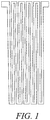
- Figure 1 illustrates the serpentine screen printed paste pattern used in the Comparative Experiment and the Examples.
- the invention relates to a paste composition for forming a solderable polyimide-based polymer thick film (PTF) conductor and a process for forming the conductor utilizing the paste.
- the paste is typically used In an electrical device to form an electrical conductor that is solderable has good adhesion and thereby provides for electrical connections.
- the main components of the instant polyimide-based polymer thick film paste composition are an electrically conductive metal powder, a polyimide polymer, an organosilicon compound and an organic solvent,
- the electrically conductive metal powder in the present polymer thick film composition is a powder of electrically conductive metal particles.
- the electrically conductive metal is selected from the group consisting of Ag, Cu, Au, Pd, Pt, Sn, Al, Ni and mixtures thereof
- the conductive particles may include silver (Ag).
- the conductive particles may, for example, include one or more of the following: Ag, Cu, Au, Pd, Pt, Sn, Al, Ni, Ag-Pd and Pt-Au.
- the conductive particles may include one or more of the following: (1) Al, Cu, Au, Ag, Pd and Pt; (2) an alloy of Al, Cu, Au, Ag, Pd and Pt; and (3) mixtures thereof.
- the conductive particles may include one of the above mentioned metals coated with another of the metals, e.g., Ag-coated Cu, Ag-coated-Ni. An embodiment may contain a mixture of any of the above.
- the metal when it is silver, it can be in the form of silver metal, alloys of silver or mixtures thereof.
- the silver can also be in the form of silver oxide (Ag 2 O), silver salts such as AgCl, AgNO 3 , AgOOCCH 3 (silver acetate), AgOOCF 3 (silver trifluoroacetate), silver orthophosphate (Ag 3 PO 4 ) or mixtures thereof.
- silver oxide Ag 2 O
- silver salts such as AgCl, AgNO 3 , AgOOCCH 3 (silver acetate), AgOOCF 3 (silver trifluoroacetate), silver orthophosphate (Ag 3 PO 4 ) or mixtures thereof.
- Other forms of silver compatible with the other thick-film paste components can also be used.
- the source of the electrically conductive metal can be in a flake form, a spherical form, a granular form, a crystalline form, other irregular forms and mixtures thereof.
- the concentration of the electrically conductive metal be as high as possible while maintaining other required characteristics of the paste composition that relate to either processing or final use.
- the electrically conductive metal is from 60 to 95 wt% of the polymer thick film paste composition. In a further embodiment, the source of the electrically conductive metal is from about 75 to about 90 wt% of the solid components of the thick film paste composition.
- the electrically conductive metal is silver and the silver is from 60 to 95 wt% of the polymer thick film paste composition. In another embodiment, the silver is from about 75 to about 90 wt% of the solid components of the thick film paste composition. As used herein, weight percent is written as wt%.
- the particle size of the electrically conductive metal is not subject to any particular limitation.
- the average particle size may be less than 10 microns, and, in a further embodiment, no more than 5 microns. In an aspect, the average particle size may be 0.1 to 5 microns, for example.
- particle size is intended to mean “average particle size”; “average particle size” means the 50% volume distribution size.
- the 50% volume distribution size can be denoted as D 50 .
- Volume distribution size may be determined by a number of methods understood by one of skill in the art, including but not limited to laser diffraction and dispersion method using a Microtrac particle size analyzer (Montgomeryville, PA). Laser light scattering, e.g., using a model LA-910 particle size analyzer available commercially from Horiba Instruments Inc. (Irvine, CA), may also be employed.
- a polyimide polymer that can withstand temperatures up to 320°C can be used in the paste composition used in the instant process.
- the polyimide polymer is represented by formula I: wherein X is C(CH 3 ) 2 , O, S(O) 2 , C(CF 3 ) 2 , O-Ph-C(CH 3 ) 2 -Ph-O, O-Ph-O- or a mixture of two or more of C(CH 3 ) 2 , O, S(O) 2 , C(CF 3 ) 2 , O-Ph-C(CH 3 ) 2 -Ph-O, O-Ph-O-; wherein Y is a diamine component or a mixture of diamine components selected from the group consisting of:m-phenylenediamine (MPD), 3,4'-diaminodiphenyl ether (3,4'-ODA), 4,4'-diamino-2,2'-bis(trifluoromethyl)biphenyl (TFMB), 3,3'-diaminodiphenyl sulfone (3,3'-DDS),
- the polyimide can be prepared in the dry and powdered state by reacting monomers 2,2'-Bis(trifluoromethyl)-4,4'-diamino biphenyl (TFMB), 2,2Bis(3-amino-4-hydroxyphenyl)hexafluoropropane (6F-AP) and Hexafluoroisopropylidenebis-phthalic dianhydride. (6-FDA).
- TFMB 2,2'-Bis(trifluoromethyl)-4,4'-diamino biphenyl
- 6F-AP 2,2Bis(3-amino-4-hydroxyphenyl)hexafluoropropane
- 6-FDA Hexafluoroisopropylidenebis-phthalic dianhydride
- the polyimide polymer is from 2 to 6 wt% of the polymer thick film paste composition.
- the ratio of the weight of the electrically conductive metal powder to the weight of the polyimide polymer is between 13 and 40.
- organosilicon compound is polydimethylsiloxane (PDMS).
- the electrically conductive metal powder is dispersed in and the polyimide polymer is dissolved in the organic solvent.
- the electrically conductive metal powder is dispersed by mechanical mixing to form a paste like composition having suitable consistency and rheology for printing.
- the solvent must be one which can dissolve the polyimide polymer and in which the electrically conductive metal powder is dispersible with an adequate degree of stability.
- the organic solvent is one that can be boiled off at relatively low temperature.
- the rheological properties of the solvent must be such that they lend good application properties to the composition. Such properties include dispersion of the electrically conductive metal powder with an adequate degree of stability, good application of composition, appropriate viscosity, thixotropy, appropriate wettability of the substrate and the electrically conductive metal powder and a good drying rate.
- Solvents suitable for use in the polyimide-based polymer thick film paste composition are acetates and terpenes such as alpha- or beta-terpineol or mixtures thereof with other solvents such as kerosene, dibutylphthalate, butyl carbitol, butyl carbitol acetate, hexylene glycol and high boiling alcohols and alcohol esters.
- solvents such as glycol ethers, ketones, esters and other solvents of like boiling points (in the range of 180°C to 250°C), and mixtures thereof may be used.
- the solvent is one or more components selected from the group consisting butyl carbitol acetate, dibasic acetates, diethyl adipate and triethylphosphate. Various combinations of these and other solvents are formulated to obtain the viscosity and volatility requirements desired. In addition, volatile liquids for promoting rapid hardening after application on the substrate may be included in the organic vehicle.
- screen-printing is expected to be a common method for the deposition of polymer thick film conductive compositions
- other conventional methods including stencil printing, syringe dispensing or other deposition or coating techniques may be utilized.
- the organic solvent is present up to 25 wt % of the total weight of the paste composition.
- the polymer thick film paste composition is deposited on a substrate typical of those used in electric devices.
- the substrate is impermeable to gases and moisture.
- the substrate can be a sheet of flexible material.
- the flexible material can be an impermeable material such as a polyimide film, e.g. Kapton®.
- the material can also be a polyester, e.g. polyethylene terephthalate, or a composite material made up of a combination of plastic sheet with optional metallic or dielectric layers deposited thereupon.
- the deposition of the polymer thick film conductive composition is performed preferably by screen printing, although other deposition techniques such as stencil printing, syringe dispensing or coating techniques can be utilized. In the case of screen-printing, the screen mesh size controls the thickness of deposited thick film.
- the deposited thick film conductive composition is dried, i.e., the solvent is evaporated, by exposure to heat, e.g. at 130°C for minutes.
- the paste is then cured by heating at a temperature of 320 to 380°C for at least 30 minutes to form the solderable polyimide-based polymer thick film conductor.
- the paste is cured by heating at a temperature of 330 to 380°C for at least 1 hour.
- the paste is cured by heating at a temperature of 330 to 380°C for at least 1 hour.
- the substrates used in the Examples were Kapton® 500HPP-ST and Kapton® 200RS100 films (obtained from the DuPont Co, Wilmington, DE) and used as received after cut into 2.5" x 3.5" pieces and alumina (AD-96) substrates (obtained from CoorsTek, Golden, CO) used with no further cleaning.
- the polyimide polymer used in the Comparative Experiments and the Examples was prepared as described above by reacting TFMB, 6F-AP and 6-FDA. in a ratio of 33/10/57.
- Adhesion was measured by a Scotch® Tape test in which the tape was applied to the cured sample and then pulled off. The adhesion was judged on a scale of from poor (>10% peeling) to good ( ⁇ 1% peeling).
- the SAC alloy with a composition of Sn96.5%Ag3.0%Cu0.5% was used for the solder wetting test. Either Alpha 611 or Kester 952 flux was used. In the solder wetting test the cured samples were typically dipped for 1 - 3 seconds into the SAC alloy pot that was kept at 225 - 250°C.
- a screen printable Ag composition was prepared using silver flakes having an average particle size of 3-4 micron.
- the components of the PTF silver conductor composition were: 84 wt % silver powder 3.4 wt% polyimide 5.3 wt% butylcarbitol acetate 2 wt% dibasic acetates (DBE-3) 5.3 wt% diethyl adipate wherein the wt% are based on the total weight of the composition.
- This composition contained no organosilicon compound.
- the components were combined and mixed for 30-60 seconds in a Thinky-type mixer, and then roll-milled.
- the composition was used to screen print a 600 square serpentine pattern (shown in Figure 1 ) on Kapton® 500HPP-ST. Using a 325 mesh stainless steel screen, several patterns were printed, and the silver paste was dried at 130°C for 10 min.
- the measured line resistance from the samples was 7.7 ⁇ .
- the average conductor thickness over the 600 square pattern was determined to be 12.7 ⁇ m using a profilometer. Therefore the resistivity was calculated to be 6.5 m ⁇ / ⁇ /mil.
- Some of the samples cured at 130°C for 10 min were cured further for 1 h at 300°C to give an average resistivity of 1.8 m ⁇ / ⁇ /mil.
- Solder wettability was tested in the manner described above using the parts cured at 130°C/300°C. The samples showed near 100% solder wetting, and adhesion found to be good. However, the samples cured at 130°C for 10 min were also cured further at 360°C for 5 h and showed a cohesive failure in adhesion.
- a screen printable Ag composition was prepared using silver flakes having an average particle size of 3-4 micron.
- the components of the PTF silver conductor composition were: 79.7 wt% silver powder 4 wt% polyimide 16.1 wt% triethylphosphate 0.2 wt% oleic acid wherein the wt% are based on the total weight of the composition.
- This composition contained no organosilicon compound.
- the components were combined and mixed for 30-60 seconds in a Thinky-type mixer, and then roll-milled.
- the composition was used to screen print a 600 square serpentine pattern (shown in Figure 1 ) on Kapton® 500HPP-ST. Using a 325 mesh stainless steel screen, several patterns were printed, and the silver paste was dried at 130°C for 10 min.
- the measured line resistance from the samples was 6.7 ⁇ .
- the average conductor thickness over the 600 square pattern was determined to be 13.8 ⁇ m using a profilometer. Therefore the resistivity was calculated to be 6.1 m ⁇ / ⁇ /mil.
- Some of the samples were cured further for 1 h at 300°C to give an average resistivity of 1.9 m ⁇ / ⁇ /mil.
- Solder wettability was tested in the manner described above using the parts cured at 130°C/300°C. The samples showed near 100% solder wetting, and adhesion found to be good. However, the samples cured at 130°C for 10 min were also cured further at 360°C for 5 h and showed a cohesive failure in adhesion.
- a screen printable Ag composition was prepared using silver flakes having an average particle size of 3-4 micron.
- the components of the PTF silver conductor composition were: 85.4 wt% silver powder 2.6 wt% polyimide 11.5 wt% triethylphosphate 0.5 wt% silicon oil (PDMS) wherein the wt% are based on the total weight of the composition.
- This composition contained 0.5 wt% organosilicon compound.
- the components were combined and mixed for 30-60 seconds in a Thinky-type mixer, and then roll-milled.
- the composition was used to screen print a 600 square serpentine pattern (shown in Figure 1 ) on Kapton® 500HPP-ST. Using a 200 mesh stainless steel screen, several patterns were printed, and the silver paste was dried at 130°C for 10 min, and then 300°C for 1 h. The average resistivity of 7.6 m ⁇ / ⁇ /mil was obtained. Solder wettability was tested in the manner described above using the samples. The samples showed less than 80% solder wetting, but no adhesion failure was observed.
- Some printed samples were also cured at 130°C for 10 min, and then cured further at 360°C for 5 h. Severe adhesive failure was observed and near 100% peeling was observed by the tape peel test.
- a screen printable Ag composition was prepared using silver flakes having an average particle size of 3-4 micron.
- the components of the PTF silver conductor composition were: 83.85 wt % silver powder 3.4 wt% polyimide 5.3 wt% butylcarbitol acetate 2.1 wt% dibasic acetates (DBE-3) 5.3 wt% diethyl adipate 0.05 wt% silicon oil wherein the wt% are based on the total weight of the composition.
- This composition contained 0.05 wt% organosilicon compound.
- the components were combined and mixed for 30-60 seconds in a Thinky-type mixer, and then roll-milled.
- the composition was used to screen print a 600 square serpentine pattern (shown in Figure 1 ) on Kapton® 500HPP-ST. Using a 325 mesh stainless steel screen, several patterns were printed, and the silver paste was dried at 130°C for 10 min and then at 200°C for 30 min.
- the measured line resistance from the samples was 4.53 ⁇ .
- the average conductor thickness over the 600 square pattern was determined to be 8.97 ⁇ m using a profilometer. Therefore the resistivity was calculated to be 2.7 m ⁇ / ⁇ /mil.
- a screen printable Ag composition was prepared using silver flakes having an average particle size of 3-4micron.
- the components of the PTF silver conductor composition were: 83.6 wt % silver powder 3.4 wt% polyimide 5.3 wt% butylcarbitol acetate 2 wt% dibasic acetates (DBE-3) 5.3 wt% diethyl adipate 0.4 wt% silicon oil (PDMS) wherein the wt% are based on the total weight of the composition.
- This composition contained 0.4 wt% organosilicon compound.
- the components were combined and mixed for 30-60 seconds in a Thinky-type mixer, and then roll-milled.
- the composition was used to screen print a 600 square serpentine pattern (shown in Figure 1 ) on Kapton® 500HPP-ST. Using a 325 mesh stainless steel screen, several patterns were printed, and the silver paste was dried at 130°C for 10 min, and then at 200°C for 30 min. The measured line resistance from the samples was 4.62 ⁇ .
- the samples were cured further for 5h at 360°C to give an average resistance of 3.43 ⁇ .
- the average conductor thickness over the 600 square pattern was determined to be 12.99 ⁇ m using a profilometer. Therefore the resistivity was calculated to be 3.0 m ⁇ / ⁇ /mil.
- Some of the samples were cured further for 5h at 360°C,however, adhesive failure was observed from some of the samples as cured.
- the tape peel test gave near 100% adhesive failure.
- a screen printable Ag composition was prepared using silver flakes having an average particle size of 3-4 micron.
- the components of the PTF silver conductor composition were: 83.4 wt % silver powder 3.4 wt% polyimide 5.3 wt% butylcarbitol acetate 2.2 wt% dibasic acetates (DBE-3) 5.4 wt% diethyl adipate 0.2 wt% silicon oil wherein the wt% are based on the total weight of the composition.
- the ratio of the weight of the silver powder to the weight of the polyimide polymer was 24.5. This composition contained 0.2 wt% organosilicon compound.
- the components were combined and mixed for 30-60 seconds in a Thinky-type mixer, and then roll-milled.
- the composition was used to screen print a 600 square serpentine pattern (shown in Figure 1 ) on Kapton® 500HPP-ST. Using a 200 mesh stainless steel screen, several patterns were printed, and the silver paste was dried at 130°C for 10 min and then cured at 300°C for 1h, which gave resistivity of 4.4 m ⁇ / ⁇ /mil.
- Solder wettability was also tested in the manner described above using the parts cured at 130°C/300°C. The samples showed 100% solder wetting. Adhesion was tested for the samples and was found to be good.
- Some of the printed samples were also cured at 130°C for 10 min , and then additionally for 5 h at 360°C to give an average resistivity of 3.2 m ⁇ / ⁇ /mil. No adhesion failure was observed. The samples showed near 100% solder wetting.
- a screen printable Ag composition was prepared using silver flakes having an average particle size of 3-4 micron.
- the components of the PTF silver conductor composition were: 79.1 wt% silver powder 4 wt% polyimide 16.5 wt% triethylphosphate 0.2 wt% oleic acid 0.2 wt% silicon oil (PDMS) wherein the wt% are based on the total weight of the composition.
- the ratio of the weight of the silver powder to the weight of the polyimide polymer was 19.8.
- This composition contained 0.2 wt% organosilicon compound.
- the components were combined and mixed for 30-60 seconds in a Thinky-type mixer, and then roll-milled.
- the composition was used to screen print a 600 square serpentine pattern (shown in Figure 1 ) on Kapton® 500HPP-ST. Using a 200 mesh stainless steel screen, several patterns were printed, and the silver paste was cured at 130°C for 10 min, and then 300°C for 1h to give an average resistivity of 3.9 m ⁇ / ⁇ /mil.
- Solder wettability was tested in the manner described above using the samples. The samples showed near 100% solder wetting. Adhesion was tested for the samples and was found to be good.
- a screen printable Ag composition was prepared using silver flakes having an average particle size of 3-4 micron.
- the components of the PTF silver conductor composition were: 85.7 wt% silver powder 2.6 wt% polyimide 11.4 wt% triethylphosphate 0.3 wt% silicon oil (PDMS) wherein the wt% are based on the total weight of the composition.
- the ratio of the weight of the silver powder to the weight of the polyimide polymer was 33.
- This composition contained 0.3 wt% organosilicon compound.
- the components were combined and mixed for 30-60 seconds in a Thinky-type mixer, and then roll-milled.
- the composition was used to screen print a 600 square serpentine pattern (shown in Figure 1 ) on Kapton® 500HPP-ST. Using a 325 mesh stainless steel screen, several patterns were printed, and the silver paste was cured at 130°C for 10 min, and then 300°C for 1h to give an average resistivity of 5.3 m ⁇ / ⁇ /mil. Solder wettability was tested in the manner described above using the samples. The samples showed nearly 100% solder wetting. No adhesion failure was observed by the tape peel test.
Description
- The invention is directed to a paste composition for forming a solderable polyimide-based polymer thick film (PTF) conductor and a process for forming the conductor utilizing the paste
- . Generally, a thick film composition comprises a functional phase that imparts appropriate electrically functional properties to the composition. The functional phase comprises electrically functional powders dispersed in an organic solvent containing a polymer. These compositions will typically contain a binder, e.g., a glass frit. Such a composition is fired to burn out the polymer and solvent and to impart the electrically functional properties. However, in the case of a polymer thick film, the polymer remains as an integral part of the composition after drying and only the solvent is removed. A processing requirement may include a heat treatment such as curing as known to those skilled in the art of polymer thick film technology.
- Many PTF compositions are only stable up to approximately 200°C and therefore do not lend them to soldering as this is done at temperatures of 200 to 260°C. Further, many current PTF electrode compositions do not wet well with solder and do not possess good adhesion to the substrate after soldering.
- It is therefore a primary objective of this invention to produce a PTF paste composition which can be used to form a solderable conductor that adheres to the underlying substrate after soldering and a process for forming such a conductor.
- The invention provides a polyimide-based polymer thick film paste composition for forming a solderable polyimide-based polymer thick film conductor, the paste composition comprising:
- (a) 60-95 wt% of an electrically conductive metal powder;
- (b) 2-6 wt% of a polyimide polymer;
- (c) 0.10-0.35 wt% of polydimethylsiloxane; and
- (d) an organic solvent,
- In an embodiment, the polyimide polymer is represented by formula I:

- i. if X is O, then Y is not m-phenylenediamine (MPD), bis-(4-(4-aminophenoxy)phenyl)sulfone (BAPS) and 3,4'-diaminodiphenyl ether (3,4'-ODA); BAPP, APB-133, or bisaniline-M;
- ii. if X is S(O)2, then Y is not 3,3'-diaminodiphenyl sulfone (3,3'-DDS);
- iii. if X is C(CF3)2, then Y is not m-phenylenediamine (MPD), bis-(4-(4-aminophenoxy)phenyl)sulfone (BAPS), 9,9-bis(4-aminophenyl)fluorene (FDA), or 3,3'-diaminodiphenyl sulfone (3,3'-DDS); and
- iv. if X is O-Ph-C(CH3)2-Ph-O or O-Ph-O-, then Y is not m-phenylene diamine (MPD), FDA, 3,4'-ODA, DAM, BAPP, APB-133, or bisaniline-M.
- The invention also provides an electrical device containing a solderable polyimide-based polymer thick film conductor formed from the paste composition of the invention.
- The invention further provides a process for forming a solderable polyimide-based polymer thick film conductor using the instant paste composition, comprising the steps of:
- (i) providing a substrate;
- (ii) preparing a paste composition comprising:
- (a) 60-95 wt% of an electrically conductive metal powder;
- (b) 2-6 wt% of a polyimide polymer;
- (c) 0.10-0.35 wt% of polydimethylsiloxane; and
- (d) an organic solvent,
wherein the wt% are based on the total weight of the paste composition, the electrically conductive metal powder and the polydimethylsiloxane is dispersed in and the polyimide polymer is dissolved in the organic solvent and the ratio of the weight of the electrically conductive metal powder to the weight of the polyimide polymer is between 13 and 40.
- (iii) applying the paste composition in the desired pattern onto the substrate; and
- (iv) curing the paste composition applied in step (iii) by heating at a temperature of 320 to 380°C for at least 30 minutes.
- In one embodiment the paste composition is fired at temperatures of from 320 to 380°C for at least 30 minutes. In another embodiment, the paste composition is fired at temperatures of from 320 to 380°C for at least 1 hour. In still another embodiment the paste composition is fired at temperatures of from 330 to 380°C for at least I hour and in other embodiments for 5 hours.
- In one embodiment after step (iii) but before step (iv) the paste composition applied in step (iii) is dried by heating at a temperature sufficient to remove the organic solvent.
- The invention also provides an electrical device containing a solderable polyimide-based polymer thick film conductor formed using the process of the invention.
-
Figure 1 illustrates the serpentine screen printed paste pattern used in the Comparative Experiment and the Examples. - The invention relates to a paste composition for forming a solderable polyimide-based polymer thick film (PTF) conductor and a process for forming the conductor utilizing the paste. The paste is typically used In an electrical device to form an electrical conductor that is solderable has good adhesion and thereby provides for electrical connections.
- The main components of the instant polyimide-based polymer thick film paste composition are an electrically conductive metal powder, a polyimide polymer, an organosilicon compound and an organic solvent,
- The electrically conductive metal powder in the present polymer thick film composition is a powder of electrically conductive metal particles.
- In one embodiment the electrically conductive metal is selected from the group consisting of Ag, Cu, Au, Pd, Pt, Sn, Al, Ni and mixtures thereof In an embodiment, the conductive particles may include silver (Ag). In a further embodiment, the conductive particles may, for example, include one or more of the following: Ag, Cu, Au, Pd, Pt, Sn, Al, Ni, Ag-Pd and Pt-Au. In another embodiment, the conductive particles may include one or more of the following: (1) Al, Cu, Au, Ag, Pd and Pt; (2) an alloy of Al, Cu, Au, Ag, Pd and Pt; and (3) mixtures thereof. In still another embodiment, the conductive particles may include one of the above mentioned metals coated with another of the metals, e.g., Ag-coated Cu, Ag-coated-Ni. An embodiment may contain a mixture of any of the above.
- When the metal is silver, it can be in the form of silver metal, alloys of silver or mixtures thereof. The silver can also be in the form of silver oxide (Ag2O), silver salts such as AgCl, AgNO3, AgOOCCH3 (silver acetate), AgOOCF3 (silver trifluoroacetate), silver orthophosphate (Ag3PO4) or mixtures thereof. Other forms of silver compatible with the other thick-film paste components can also be used.
- The source of the electrically conductive metal can be in a flake form, a spherical form, a granular form, a crystalline form, other irregular forms and mixtures thereof.
- To attain high conductivity in a finished conductive structure, it is generally preferable to have the concentration of the electrically conductive metal be as high as possible while maintaining other required characteristics of the paste composition that relate to either processing or final use.
- In one embodiment, the electrically conductive metal is from 60 to 95 wt% of the polymer thick film paste composition. In a further embodiment, the source of the electrically conductive metal is from about 75 to about 90 wt% of the solid components of the thick film paste composition.
- In one embodiment, the electrically conductive metal is silver and the silver is from 60 to 95 wt% of the polymer thick film paste composition. In another embodiment, the silver is from about 75 to about 90 wt% of the solid components of the thick film paste composition. As used herein, weight percent is written as wt%.
- The particle size of the electrically conductive metal is not subject to any particular limitation. In an embodiment, the average particle size may be less than 10 microns, and, in a further embodiment, no more than 5 microns. In an aspect, the average particle size may be 0.1 to 5 microns, for example. As used herein, "particle size" is intended to mean "average particle size"; "average particle size" means the 50% volume distribution size. The 50% volume distribution size can be denoted as D50. Volume distribution size may be determined by a number of methods understood by one of skill in the art, including but not limited to laser diffraction and dispersion method using a Microtrac particle size analyzer (Montgomeryville, PA). Laser light scattering, e.g., using a model LA-910 particle size analyzer available commercially from Horiba Instruments Inc. (Irvine, CA), may also be employed.
- A polyimide polymer that can withstand temperatures up to 320°C can be used in the paste composition used in the instant process.
- In an embodiment, the polyimide polymer is represented by formula I:

- i. if X is O, then Y is not m-phenylenediamine (MPD), bis-(4-(4-aminophenoxy)phenyl)sulfone (BAPS) and 3,4'-diaminodiphenyl ether (3,4'-ODA); BAPP, APB-133, or bisaniline-M;
- ii. if X is S(O)2, then Y is not 3,3'-diaminodiphenyl sulfone (3,3'-DDS);
- iii. if X is C(CF3)2, then Y is not m-phenylenediamine (MPD), bis-(4-(4-aminophenoxy)phenyl)sulfone (BAPS), 9,9-bis(4-aminophenyl)fluorene (FDA), or 3,3'-diaminodiphenyl sulfone (3,3'-DDS); and
- iv. if X is O-Ph-C(CH3)2-Ph-O or O-Ph-O-, then Y is not m-phenylene diamine (MPD), FDA, 3,4'-ODA, DAM, BAPP, APB-133, or bisaniline-M.
- In one embodiment the polyimide can be prepared in the dry and powdered state by reacting monomers 2,2'-Bis(trifluoromethyl)-4,4'-diamino biphenyl (TFMB), 2,2Bis(3-amino-4-hydroxyphenyl)hexafluoropropane (6F-AP) and Hexafluoroisopropylidenebis-phthalic dianhydride. (6-FDA). in a ratio of 33/10/57 (TFMB/6F-AP/6-FDA) through the well-known process of first making polyamic acid in N,N-Dimethylacetamide (DMAC) solvent, controlling the molecular weight of said polyamic acid with end-capping additives, then chemically imidizing and precipitating the polyimide polymer using methanol neat additions to the DMAC solution. The precipitate was washed several times with methanol neat, filtered and then dried at approximately 200°C to form a dry and handleable powder and to reduce DMAC residuals to below 0.1% weight. The resulting powder can be dried and stored at room temperature or dissolved in a solvent in preparation for forming the paste composition.
- In one embodiment, the polyimide polymer is from 2 to 6 wt% of the polymer thick film paste composition.
- In one embodiment, the ratio of the weight of the electrically conductive metal powder to the weight of the polyimide polymer is between 13 and 40.
- The presence of 0.1-0.35 wt% organosilicon compound is critical to curing the paste at temperatures of 320 to 380°C and producing solderable thick film conductors that exhibit good adhesion. The organosilicon compound is polydimethylsiloxane (PDMS).
- The electrically conductive metal powder is dispersed in and the polyimide polymer is dissolved in the organic solvent. The electrically conductive metal powder is dispersed by mechanical mixing to form a paste like composition having suitable consistency and rheology for printing.
- The solvent must be one which can dissolve the polyimide polymer and in which the electrically conductive metal powder is dispersible with an adequate degree of stability. The organic solvent is one that can be boiled off at relatively low temperature. The rheological properties of the solvent must be such that they lend good application properties to the composition. Such properties include dispersion of the electrically conductive metal powder with an adequate degree of stability, good application of composition, appropriate viscosity, thixotropy, appropriate wettability of the substrate and the electrically conductive metal powder and a good drying rate.
- Solvents suitable for use in the polyimide-based polymer thick film paste composition are acetates and terpenes such as alpha- or beta-terpineol or mixtures thereof with other solvents such as kerosene, dibutylphthalate, butyl carbitol, butyl carbitol acetate, hexylene glycol and high boiling alcohols and alcohol esters. In embodiments of the present invention, solvents such as glycol ethers, ketones, esters and other solvents of like boiling points (in the range of 180°C to 250°C), and mixtures thereof may be used. In one embodiment, the solvent is one or more components selected from the group consisting butyl carbitol acetate, dibasic acetates, diethyl adipate and triethylphosphate. Various combinations of these and other solvents are formulated to obtain the viscosity and volatility requirements desired. In addition, volatile liquids for promoting rapid hardening after application on the substrate may be included in the organic vehicle.
- Although screen-printing is expected to be a common method for the deposition of polymer thick film conductive compositions, other conventional methods including stencil printing, syringe dispensing or other deposition or coating techniques may be utilized.
- In one embodiment, the organic solvent is present up to 25 wt % of the total weight of the paste composition.
- The polymer thick film paste composition is deposited on a substrate typical of those used in electric devices. In a typical embodiment, the substrate is impermeable to gases and moisture. The substrate can be a sheet of flexible material. The flexible material can be an impermeable material such as a polyimide film, e.g. Kapton®. The material can also be a polyester, e.g. polyethylene terephthalate, or a composite material made up of a combination of plastic sheet with optional metallic or dielectric layers deposited thereupon.
- The deposition of the polymer thick film conductive composition is performed preferably by screen printing, although other deposition techniques such as stencil printing, syringe dispensing or coating techniques can be utilized. In the case of screen-printing, the screen mesh size controls the thickness of deposited thick film.
- The deposited thick film conductive composition is dried, i.e., the solvent is evaporated, by exposure to heat, e.g. at 130°C for minutes. The paste is then cured by heating at a temperature of 320 to 380°C for at least 30 minutes to form the solderable polyimide-based polymer thick film conductor. In another embodiment the paste is cured by heating at a temperature of 330 to 380°C for at least 1 hour. In another embodiment, the paste is cured by heating at a temperature of 330 to 380°C for at least 1 hour.
- The substrates used in the Examples were Kapton® 500HPP-ST and Kapton® 200RS100 films (obtained from the DuPont Co, Wilmington, DE) and used as received after cut into 2.5" x 3.5" pieces and alumina (AD-96) substrates (obtained from CoorsTek, Golden, CO) used with no further cleaning.
- The polyimide polymer used in the Comparative Experiments and the Examples was prepared as described above by reacting TFMB, 6F-AP and 6-FDA. in a ratio of 33/10/57.
- A silicone oil purchased from Aldrich (product # 146153) was used as a source of polydimethylsiloxane (PDMS).
- Adhesion was measured by a Scotch® Tape test in which the tape was applied to the cured sample and then pulled off. The adhesion was judged on a scale of from poor (>10% peeling) to good (<1% peeling).
- The SAC alloy with a composition of Sn96.5%Ag3.0%Cu0.5% was used for the solder wetting test. Either Alpha 611 or Kester 952 flux was used. In the solder wetting test the cured samples were typically dipped for 1 - 3 seconds into the SAC alloy pot that was kept at 225 - 250°C.
- A screen printable Ag composition was prepared using silver flakes having an average particle size of 3-4 micron. The components of the PTF silver conductor composition were:
84 wt % silver powder 3.4 wt% polyimide 5.3 wt% butylcarbitol acetate 2 wt% dibasic acetates (DBE-3) 5.3 wt% diethyl adipate - The components were combined and mixed for 30-60 seconds in a Thinky-type mixer, and then roll-milled. The composition was used to screen print a 600 square serpentine pattern (shown in
Figure 1 ) on Kapton® 500HPP-ST. Using a 325 mesh stainless steel screen, several patterns were printed, and the silver paste was dried at 130°C for 10 min. The measured line resistance from the samples was 7.7 Ω. The average conductor thickness over the 600 square pattern was determined to be 12.7 µm using a profilometer. Therefore the resistivity was calculated to be 6.5 mΩ/□/mil. Some of the samples cured at 130°C for 10 min were cured further for 1 h at 300°C to give an average resistivity of 1.8 mΩ/□/mil. - Solder wettability was tested in the manner described above using the parts cured at 130°C/300°C. The samples showed near 100% solder wetting, and adhesion found to be good. However, the samples cured at 130°C for 10 min were also cured further at 360°C for 5 h and showed a cohesive failure in adhesion.
- A screen printable Ag composition was prepared using silver flakes having an average particle size of 3-4 micron. The components of the PTF silver conductor composition were:
79.7 wt% silver powder 4 wt% polyimide 16.1 wt% triethylphosphate 0.2 wt% oleic acid - The components were combined and mixed for 30-60 seconds in a Thinky-type mixer, and then roll-milled. The composition was used to screen print a 600 square serpentine pattern (shown in
Figure 1 ) on Kapton® 500HPP-ST. Using a 325 mesh stainless steel screen, several patterns were printed, and the silver paste was dried at 130°C for 10 min. The measured line resistance from the samples was 6.7 Ω. The average conductor thickness over the 600 square pattern was determined to be 13.8 µm using a profilometer. Therefore the resistivity was calculated to be 6.1 mΩ/□/mil. Some of the samples were cured further for 1 h at 300°C to give an average resistivity of 1.9 mΩ/□/mil. - Solder wettability was tested in the manner described above using the parts cured at 130°C/300°C. The samples showed near 100% solder wetting, and adhesion found to be good. However, the samples cured at 130°C for 10 min were also cured further at 360°C for 5 h and showed a cohesive failure in adhesion.
- A screen printable Ag composition was prepared using silver flakes having an average particle size of 3-4 micron. The components of the PTF silver conductor composition were:
85.4 wt% silver powder 2.6 wt% polyimide 11.5 wt% triethylphosphate 0.5 wt% silicon oil (PDMS) - The components were combined and mixed for 30-60 seconds in a Thinky-type mixer, and then roll-milled. The composition was used to screen print a 600 square serpentine pattern (shown in
Figure 1 ) on Kapton® 500HPP-ST. Using a 200 mesh stainless steel screen, several patterns were printed, and the silver paste was dried at 130°C for 10 min, and then 300°C for 1 h. The average resistivity of 7.6 mΩ/□/mil was obtained. Solder wettability was tested in the manner described above using the samples. The samples showed less than 80% solder wetting, but no adhesion failure was observed. - Some printed samples were also cured at 130°C for 10 min, and then cured further at 360°C for 5 h. Severe adhesive failure was observed and near 100% peeling was observed by the tape peel test.
- A screen printable Ag composition was prepared using silver flakes having an average particle size of 3-4 micron. The components of the PTF silver conductor composition were:
83.85 wt % silver powder 3.4 wt% polyimide 5.3 wt% butylcarbitol acetate 2.1 wt% dibasic acetates (DBE-3) 5.3 wt% diethyl adipate 0.05 wt% silicon oil - The components were combined and mixed for 30-60 seconds in a Thinky-type mixer, and then roll-milled. The composition was used to screen print a 600 square serpentine pattern (shown in
Figure 1 ) on Kapton® 500HPP-ST. Using a 325 mesh stainless steel screen, several patterns were printed, and the silver paste was dried at 130°C for 10 min and then at 200°C for 30 min. The measured line resistance from the samples was 4.53 Ω. The average conductor thickness over the 600 square pattern was determined to be 8.97 µm using a profilometer. Therefore the resistivity was calculated to be 2.7 mΩ/□/mil. - Some samples were cured further at 360°C for 5 h to give an average resistivity of 1.2 mΩ/□/mil. However, adhesion was tested for the samples and was found to be poor.
- A screen printable Ag composition was prepared using silver flakes having an average particle size of 3-4micron. The components of the PTF silver conductor composition were:
83.6 wt % silver powder 3.4 wt% polyimide 5.3 wt% butylcarbitol acetate 2 wt% dibasic acetates (DBE-3) 5.3 wt% diethyl adipate 0.4 wt% silicon oil (PDMS) - The components were combined and mixed for 30-60 seconds in a Thinky-type mixer, and then roll-milled. The composition was used to screen print a 600 square serpentine pattern (shown in
Figure 1 ) on Kapton® 500HPP-ST. Using a 325 mesh stainless steel screen, several patterns were printed, and the silver paste was dried at 130°C for 10 min, and then at 200°C for 30 min. The measured line resistance from the samples was 4.62 Ω. The samples were cured further for 5h at 360°C to give an average resistance of 3.43 Ω. The average conductor thickness over the 600 square pattern was determined to be 12.99 µm using a profilometer. Therefore the resistivity was calculated to be 3.0 mΩ/□/mil. Some of the samples were cured further for 5h at 360°C,however, adhesive failure was observed from some of the samples as cured. The tape peel test gave near 100% adhesive failure. - A screen printable Ag composition was prepared using silver flakes having an average particle size of 3-4 micron. The components of the PTF silver conductor composition were:
83.4 wt % silver powder 3.4 wt% polyimide 5.3 wt% butylcarbitol acetate 2.2 wt% dibasic acetates (DBE-3) 5.4 wt% diethyl adipate 0.2 wt% silicon oil - The components were combined and mixed for 30-60 seconds in a Thinky-type mixer, and then roll-milled. The composition was used to screen print a 600 square serpentine pattern (shown in
Figure 1 ) on Kapton® 500HPP-ST. Using a 200 mesh stainless steel screen, several patterns were printed, and the silver paste was dried at 130°C for 10 min and then cured at 300°C for 1h, which gave resistivity of 4.4 mΩ/□/mil. - Solder wettability was also tested in the manner described above using the parts cured at 130°C/300°C. The samples showed 100% solder wetting. Adhesion was tested for the samples and was found to be good.
- Some of the printed samples were also cured at 130°C for 10 min , and then additionally for 5 h at 360°C to give an average resistivity of 3.2 mΩ/□/mil. No adhesion failure was observed. The samples showed near 100% solder wetting.
- A screen printable Ag composition was prepared using silver flakes having an average particle size of 3-4 micron. The components of the PTF silver conductor composition were:
79.1 wt% silver powder 4 wt% polyimide 16.5 wt% triethylphosphate 0.2 wt% oleic acid 0.2 wt% silicon oil (PDMS) - The components were combined and mixed for 30-60 seconds in a Thinky-type mixer, and then roll-milled. The composition was used to screen print a 600 square serpentine pattern (shown in
Figure 1 ) on Kapton® 500HPP-ST. Using a 200 mesh stainless steel screen, several patterns were printed, and the silver paste was cured at 130°C for 10 min, and then 300°C for 1h to give an average resistivity of 3.9 mΩ/□/mil. Solder wettability was tested in the manner described above using the samples. The samples showed near 100% solder wetting. Adhesion was tested for the samples and was found to be good. - Some of the samples were at 130°C for 10 min, and then cured further for 5h at 360°C to give an average resistivity of 2.6 mΩ/□/mil. No adhesion failure was observed. The samples showed near 100% solder wetting.
- A screen printable Ag composition was prepared using silver flakes having an average particle size of 3-4 micron. The components of the PTF silver conductor composition were:
85.7 wt% silver powder 2.6 wt% polyimide 11.4 wt% triethylphosphate 0.3 wt% silicon oil (PDMS) - The components were combined and mixed for 30-60 seconds in a Thinky-type mixer, and then roll-milled. The composition was used to screen print a 600 square serpentine pattern (shown in
Figure 1 ) on Kapton® 500HPP-ST. Using a 325 mesh stainless steel screen, several patterns were printed, and the silver paste was cured at 130°C for 10 min, and then 300°C for 1h to give an average resistivity of 5.3 mΩ/□/mil. Solder wettability was tested in the manner described above using the samples. The samples showed nearly 100% solder wetting. No adhesion failure was observed by the tape peel test. - Some printed samples were also cured at 130°C for 10 min, and then cured further at 360°C for 5 h, which gave an average resistivity of 4.6 mΩ/□/mil. The samples showed 100% solder wetting and no adhesion failure was observed for the samples.
Claims (9)
- A polyimide-based polymer thick film paste composition for forming a solderable polyimide-based polymer thick film conductor, the paste composition comprising:(a) 60-95 wt% of an electrically conductive metal powder;(b) 2-6 wt% of a polyimide polymer;(c) 0.10-0.35 wt% of polydimethylsiloxane and(d) an organic solvent,wherein the wt% are based on the total weight of the paste composition, the electrically conductive metal powder and the polydimethylsiloxane is dispersed in and the polyimide polymer is dissolved in the organic solvent and the ratio of the weight of the electrically conductive metal powder to the weight of the polyimide polymer is between 13 and 40.
- The polyimide-based polymer thick film paste composition of claim 1, said paste composition comprising: 75-90 wt% of an electrically conductive metal powder.
- The polyimide-based polymer thick film paste composition of claim 1, wherein said electrically conductive metal is selected from the group consisting of Ag, Cu, Au, Pd, Pt, Sn, Al, Ni, alloys of Ag, Cu, Au, Pd, Pt, Sn, Al, Ni, one of Ag, Cu, Au, Pd, Pt, Sn, Al, Ni coated with one of Ag, Cu, Au, Pd, Pt, Sn, Al, Ni and mixtures thereof.
- The polyimide-based polymer thick film paste composition of claim 1, wherein said electrically conductive metal is selected from the group consisting of Ag, Ag-coated Cu, Ag-coated-Ni and mixtures thereof.
- The polyimide-based polymer thick film paste composition of claim 1, wherein said polyimide polymer is represented by formula I:
 wherein X is C(CH3)2, O, S(O)2, C(CF3)2, O-Ph-C(CH3)2-Ph-O, O-Ph-O- or a mixture of two or more of C(CH3)2, O, S(O)2, C(CF3)2, O-Ph-C(CH3)2-Ph-O, O-Ph-O-;wherein Y is a diamine component or a mixture of diamine components selected from the group consisting of:m-phenylenediamine (MPD), 3,4'-diaminodiphenyl ether (3,4'-ODA),4,4'-diamino-2,2'-bis(trifluoromethyl)biphenyl (TFMB), 3,3'-diaminodiphenyl sulfone (3,3'-DDS), 4,4'-(Hexafluoroisopropylidene)bis(2-aminophenol) (6F-AP), bis-(4-(4-aminophenoxy)phenyl)sulfone (BAPS), 9,9-bis(4-aminophenyl)fluorene (FDA); 2,3,5,6-tetramethyl-1,4-phenylenediamine (DAM), 2,2-bis[4-(4-aminophenoxyphenyl)]propane (BAPP), 2,2-bis[4-(4-aminophenoxyphenyl)] hexafluoropropane (HFBAPP), 1,3-bis(3-aminophenoxy) benzene (APB-133), 2,2-bis(3-aminophenyl)hexafluoropropane, 2,2-bis(4 aminophenyl)hexafluoropropane (bis-A-AF), 4,4'-bis(4-amino-2-trifluoromethylphenoxy) biphenyl, 4,4'-[1,3-phenylenebis(1-methyl-ethylidene)], and bisaniline (bisaniline-M) with the proviso that:i. if X is O, then Y is not m-phenylenediamine (MPD), bis-(4-(4-aminophenoxy)phenyl)sulfone (BAPS) and 3,4'-diaminodiphenyl ether (3,4'-ODA); BAPP, APB-133, or bisaniline-M;ii. if X is S(O)2, then Y is not 3,3'-diaminodiphenyl sulfone (3,3'-DDS);iii. if X is C(CF3)2, then Y is not m-phenylenediamine (MPD), bis-(4-(4-aminophenoxy)phenyl)sulfone (BAPS), 9,9-bis(4-aminophenyl)fluorene (FDA), or 3,3'-diaminodiphenyl sulfone (3,3'-DDS); andiv. if X is O-Ph-C(CH3)2-Ph-O or O-Ph-O-, then Y is not m-phenylene diamine (MPD), FDA, 3,4'-ODA, DAM, BAPP, APB-133, or bisaniline-M.
 - An electrical device containing a solderable polyimide-based polymer thick film conductor formed from the polyimide-based polymer thick film paste composition of claim 1.
- A process for forming a solderable polyimide-based polymer thick film conductor, comprising the steps of:(i) providing a substrate;(ii) preparing a paste composition comprising:(a) 60-95 wt% of an electrically conductive metal powder;(b) 4-6 wt% of a polyimide polymer;(c) 0.10-0.35 wt% of polydimethylsiloxane; and(d) an organic solvent,
wherein the wt% are based on the total weight of the paste composition, the electrically conductive metal powder and the polydimethylsiloxane is dispersed in and the polyimide polymer is dissolved in the organic solvent and the ratio of the weight of the electrically conductive metal powder to the weight of the polyimide polymer is between 13 and 40.(iii) applying said paste composition in the desired pattern onto said substrate; and(iv) curing said paste composition applied in step (iii) by heating at a temperature of 320 to 380°C for at least 30 minutes to form said solderable polyimide-based polymer thick film conductor. - The process of claim 7, wherein after step (iii) but before step (iv) said paste composition applied in step (iii) is dried by heating at a temperature sufficient to remove said organic solvent.
- An electrical device containing a solderable polyimide-based polymer thick film conductor formed using the process of claim 7.
Applications Claiming Priority (2)
| Application Number | Priority Date | Filing Date | Title |
|---|---|---|---|
| US14/824,202 US9649730B2 (en) | 2015-08-12 | 2015-08-12 | Paste and process for forming a solderable polyimide-based polymer thick film conductor |
| PCT/US2016/045997 WO2017027456A1 (en) | 2015-08-12 | 2016-08-08 | Paste and process for forming a solderable polyimide–based polymer thick film conductor |
Publications (2)
| Publication Number | Publication Date |
|---|---|
| EP3335224A1 EP3335224A1 (en) | 2018-06-20 |
| EP3335224B1 true EP3335224B1 (en) | 2019-06-12 |
Family
ID=56686979
Family Applications (1)
| Application Number | Title | Priority Date | Filing Date |
|---|---|---|---|
| EP16751796.0A Active EP3335224B1 (en) | 2015-08-12 | 2016-08-08 | Paste and process for forming a solderable polyimide based polymer thick film conductor |
Country Status (5)
| Country | Link |
|---|---|
| US (1) | US9649730B2 (en) |
| EP (1) | EP3335224B1 (en) |
| JP (1) | JP6737874B2 (en) |
| CN (1) | CN108140446B (en) |
| WO (1) | WO2017027456A1 (en) |
Families Citing this family (2)
| Publication number | Priority date | Publication date | Assignee | Title |
|---|---|---|---|---|
| US20170044382A1 (en) * | 2015-08-12 | 2017-02-16 | E I Du Pont De Nemours And Company | Process for forming a solderable polyimide-based polymer thick film conductor |
| CN109776826B (en) * | 2019-01-21 | 2020-09-29 | 深圳丹邦科技股份有限公司 | Polyimide thick film, quantum carbon-based film and preparation method thereof |
Family Cites Families (21)
| Publication number | Priority date | Publication date | Assignee | Title |
|---|---|---|---|---|
| EP0143531A1 (en) * | 1983-09-30 | 1985-06-05 | Electro Materials Corp. Of America | A method of forming a solderable, electrically conductive film on a substrate and the conductive composition itself |
| JPS6183250A (en) * | 1984-09-29 | 1986-04-26 | Nitto Electric Ind Co Ltd | Electrically conductive paste composition for electronic part |
| JPH0565456A (en) * | 1991-09-09 | 1993-03-19 | Sumitomo Bakelite Co Ltd | Resin paste for airtight sealing |
| US5545429A (en) * | 1994-07-01 | 1996-08-13 | International Business Machines Corporation | Fabrication of double side fully metallized plated thru-holes, in polymer structures, without seeding or photoprocess |
| US6344157B1 (en) * | 1999-02-12 | 2002-02-05 | National Starch And Chemical Investment Holding Corporation | Conductive and resistive materials with electrical stability for use in electronics devices |
| JP2003129017A (en) * | 2001-10-25 | 2003-05-08 | Sumitomo Bakelite Co Ltd | Conductive adhesive film and semiconductor device using the same |
| US7348373B2 (en) | 2004-01-09 | 2008-03-25 | E.I. Du Pont De Nemours And Company | Polyimide compositions having resistance to water sorption, and methods relating thereto |
| US7169330B2 (en) | 2004-02-25 | 2007-01-30 | E. I. Du Pont De Nemours And Company | Composition of conductive paste |
| CN1835129B (en) * | 2005-03-16 | 2010-04-28 | E.I.内穆尔杜邦公司 | Conductive slurry-like compositions |
| US7745516B2 (en) | 2005-10-12 | 2010-06-29 | E. I. Du Pont De Nemours And Company | Composition of polyimide and sterically-hindered hydrophobic epoxy |
| JP2008106145A (en) * | 2006-10-25 | 2008-05-08 | Sekisui Chem Co Ltd | Sintering electroconductive paste |
| US8270145B2 (en) | 2007-12-04 | 2012-09-18 | Cda Processing Limited Liability Company | Screen-printable encapsulants based on soluble polybenzoxazoles |
| CN102169739B (en) * | 2011-02-25 | 2012-09-05 | 乐山新天源太阳能电力有限公司 | Nanometer aluminum paste for solar battery and manufacturing method thereof |
| JP6028727B2 (en) * | 2011-05-18 | 2016-11-16 | 戸田工業株式会社 | Copper powder, copper paste, method for producing conductive coating film and conductive coating film |
| TW201339279A (en) * | 2011-11-24 | 2013-10-01 | Showa Denko Kk | Conductive-pattern formation method and composition for forming conductive pattern via light exposure or microwave heating |
| JP5321723B1 (en) * | 2012-10-29 | 2013-10-23 | 横浜ゴム株式会社 | Conductive composition and solar battery cell |
| US9818718B2 (en) * | 2012-10-30 | 2017-11-14 | Kaken Tech Co., Ltd. | Conductive paste and die bonding method |
| JP5700864B2 (en) * | 2013-05-15 | 2015-04-15 | 石原ケミカル株式会社 | Copper fine particle dispersion, conductive film forming method, and circuit board |
| US9190188B2 (en) * | 2013-06-13 | 2015-11-17 | E I Du Pont De Nemours And Company | Photonic sintering of polymer thick film copper conductor compositions |
| JP2015032493A (en) * | 2013-08-05 | 2015-02-16 | 富士フイルム株式会社 | Composition for formation of conductive film and method of producing conductive film using the same |
| CN104650653B (en) * | 2013-11-22 | 2017-09-01 | 苏州冷石纳米材料科技有限公司 | A kind of conductive nano silver paste and preparation method thereof |
-
2015
- 2015-08-12 US US14/824,202 patent/US9649730B2/en active Active
-
2016
- 2016-08-08 JP JP2018507563A patent/JP6737874B2/en active Active
- 2016-08-08 EP EP16751796.0A patent/EP3335224B1/en active Active
- 2016-08-08 CN CN201680058560.XA patent/CN108140446B/en active Active
- 2016-08-08 WO PCT/US2016/045997 patent/WO2017027456A1/en active Application Filing
Non-Patent Citations (1)
| Title |
|---|
| None * |
Also Published As
| Publication number | Publication date |
|---|---|
| JP2018529802A (en) | 2018-10-11 |
| US20170043435A1 (en) | 2017-02-16 |
| JP6737874B2 (en) | 2020-08-12 |
| CN108140446A (en) | 2018-06-08 |
| EP3335224A1 (en) | 2018-06-20 |
| WO2017027456A1 (en) | 2017-02-16 |
| CN108140446B (en) | 2020-07-31 |
| US9649730B2 (en) | 2017-05-16 |
Similar Documents
| Publication | Publication Date | Title |
|---|---|---|
| JP6491753B2 (en) | Metal paste excellent in low-temperature sinterability and method for producing the metal paste | |
| JP7168701B2 (en) | Polyimide polymer thick film composition | |
| WO2007047384A1 (en) | Compositions comprising polyimide and hydrophobic epoxy, and methods relating thereto | |
| EP3335224B1 (en) | Paste and process for forming a solderable polyimide based polymer thick film conductor | |
| US10153075B2 (en) | Polyimide-based polymer thick film resistor composition | |
| EP3335223B1 (en) | Photonic sintering of a polymer thick film copper conductor composition | |
| US20160183328A1 (en) | Method and devices for high temperature thick film pastes | |
| EP3335226B1 (en) | Photonic sintering of a solderable polymer thick film copper conductor composition | |
| JP6737872B2 (en) | Process for forming solderable polyimide-based polymer thick film conductors | |
| JP2018529802A5 (en) | ||
| US10508217B2 (en) | Polyimide-based polymer thick film resistor composition | |
| JP3917037B2 (en) | External electrode and electronic component including the same | |
| JP5654463B2 (en) | Substances and electronic parts composed of metals and lactic acid condensates | |
| JP2018525494A5 (en) |
Legal Events
| Date | Code | Title | Description |
|---|---|---|---|
| STAA | Information on the status of an ep patent application or granted ep patent |
Free format text: STATUS: THE INTERNATIONAL PUBLICATION HAS BEEN MADE |
|
| PUAI | Public reference made under article 153(3) epc to a published international application that has entered the european phase |
Free format text: ORIGINAL CODE: 0009012 |
|
| STAA | Information on the status of an ep patent application or granted ep patent |
Free format text: STATUS: REQUEST FOR EXAMINATION WAS MADE |
|
| 17P | Request for examination filed |
Effective date: 20180201 |
|
| AK | Designated contracting states |
Kind code of ref document: A1 Designated state(s): AL AT BE BG CH CY CZ DE DK EE ES FI FR GB GR HR HU IE IS IT LI LT LU LV MC MK MT NL NO PL PT RO RS SE SI SK SM TR |
|
| AX | Request for extension of the european patent |
Extension state: BA ME |
|
| DAV | Request for validation of the european patent (deleted) | ||
| DAX | Request for extension of the european patent (deleted) | ||
| GRAP | Despatch of communication of intention to grant a patent |
Free format text: ORIGINAL CODE: EPIDOSNIGR1 |
|
| STAA | Information on the status of an ep patent application or granted ep patent |
Free format text: STATUS: GRANT OF PATENT IS INTENDED |
|
| RIC1 | Information provided on ipc code assigned before grant |
Ipc: H05K 1/09 20060101ALI20181116BHEP Ipc: H01B 1/22 20060101AFI20181116BHEP Ipc: B23K 35/22 20060101ALI20181116BHEP |
|
| INTG | Intention to grant announced |
Effective date: 20181221 |
|
| GRAS | Grant fee paid |
Free format text: ORIGINAL CODE: EPIDOSNIGR3 |
|
| GRAA | (expected) grant |
Free format text: ORIGINAL CODE: 0009210 |
|
| STAA | Information on the status of an ep patent application or granted ep patent |
Free format text: STATUS: THE PATENT HAS BEEN GRANTED |
|
| AK | Designated contracting states |
Kind code of ref document: B1 Designated state(s): AL AT BE BG CH CY CZ DE DK EE ES FI FR GB GR HR HU IE IS IT LI LT LU LV MC MK MT NL NO PL PT RO RS SE SI SK SM TR |
|
| REG | Reference to a national code |
Ref country code: GB Ref legal event code: FG4D |
|
| REG | Reference to a national code |
Ref country code: CH Ref legal event code: EP |
|
| REG | Reference to a national code |
Ref country code: AT Ref legal event code: REF Ref document number: 1143635 Country of ref document: AT Kind code of ref document: T Effective date: 20190615 |
|
| REG | Reference to a national code |
Ref country code: DE Ref legal event code: R096 Ref document number: 602016015284 Country of ref document: DE |
|
| REG | Reference to a national code |
Ref country code: IE Ref legal event code: FG4D |
|
| REG | Reference to a national code |
Ref country code: NL Ref legal event code: MP Effective date: 20190612 |
|
| REG | Reference to a national code |
Ref country code: LT Ref legal event code: MG4D |
|
| PG25 | Lapsed in a contracting state [announced via postgrant information from national office to epo] |
Ref country code: FI Free format text: LAPSE BECAUSE OF FAILURE TO SUBMIT A TRANSLATION OF THE DESCRIPTION OR TO PAY THE FEE WITHIN THE PRESCRIBED TIME-LIMIT Effective date: 20190612 Ref country code: LT Free format text: LAPSE BECAUSE OF FAILURE TO SUBMIT A TRANSLATION OF THE DESCRIPTION OR TO PAY THE FEE WITHIN THE PRESCRIBED TIME-LIMIT Effective date: 20190612 Ref country code: AL Free format text: LAPSE BECAUSE OF FAILURE TO SUBMIT A TRANSLATION OF THE DESCRIPTION OR TO PAY THE FEE WITHIN THE PRESCRIBED TIME-LIMIT Effective date: 20190612 Ref country code: SE Free format text: LAPSE BECAUSE OF FAILURE TO SUBMIT A TRANSLATION OF THE DESCRIPTION OR TO PAY THE FEE WITHIN THE PRESCRIBED TIME-LIMIT Effective date: 20190612 Ref country code: HR Free format text: LAPSE BECAUSE OF FAILURE TO SUBMIT A TRANSLATION OF THE DESCRIPTION OR TO PAY THE FEE WITHIN THE PRESCRIBED TIME-LIMIT Effective date: 20190612 Ref country code: NO Free format text: LAPSE BECAUSE OF FAILURE TO SUBMIT A TRANSLATION OF THE DESCRIPTION OR TO PAY THE FEE WITHIN THE PRESCRIBED TIME-LIMIT Effective date: 20190912 |
|
| PG25 | Lapsed in a contracting state [announced via postgrant information from national office to epo] |
Ref country code: GR Free format text: LAPSE BECAUSE OF FAILURE TO SUBMIT A TRANSLATION OF THE DESCRIPTION OR TO PAY THE FEE WITHIN THE PRESCRIBED TIME-LIMIT Effective date: 20190913 Ref country code: LV Free format text: LAPSE BECAUSE OF FAILURE TO SUBMIT A TRANSLATION OF THE DESCRIPTION OR TO PAY THE FEE WITHIN THE PRESCRIBED TIME-LIMIT Effective date: 20190612 Ref country code: RS Free format text: LAPSE BECAUSE OF FAILURE TO SUBMIT A TRANSLATION OF THE DESCRIPTION OR TO PAY THE FEE WITHIN THE PRESCRIBED TIME-LIMIT Effective date: 20190612 Ref country code: BG Free format text: LAPSE BECAUSE OF FAILURE TO SUBMIT A TRANSLATION OF THE DESCRIPTION OR TO PAY THE FEE WITHIN THE PRESCRIBED TIME-LIMIT Effective date: 20190912 |
|
| REG | Reference to a national code |
Ref country code: AT Ref legal event code: MK05 Ref document number: 1143635 Country of ref document: AT Kind code of ref document: T Effective date: 20190612 |
|
| PG25 | Lapsed in a contracting state [announced via postgrant information from national office to epo] |
Ref country code: SK Free format text: LAPSE BECAUSE OF FAILURE TO SUBMIT A TRANSLATION OF THE DESCRIPTION OR TO PAY THE FEE WITHIN THE PRESCRIBED TIME-LIMIT Effective date: 20190612 Ref country code: EE Free format text: LAPSE BECAUSE OF FAILURE TO SUBMIT A TRANSLATION OF THE DESCRIPTION OR TO PAY THE FEE WITHIN THE PRESCRIBED TIME-LIMIT Effective date: 20190612 Ref country code: CZ Free format text: LAPSE BECAUSE OF FAILURE TO SUBMIT A TRANSLATION OF THE DESCRIPTION OR TO PAY THE FEE WITHIN THE PRESCRIBED TIME-LIMIT Effective date: 20190612 Ref country code: NL Free format text: LAPSE BECAUSE OF FAILURE TO SUBMIT A TRANSLATION OF THE DESCRIPTION OR TO PAY THE FEE WITHIN THE PRESCRIBED TIME-LIMIT Effective date: 20190612 Ref country code: RO Free format text: LAPSE BECAUSE OF FAILURE TO SUBMIT A TRANSLATION OF THE DESCRIPTION OR TO PAY THE FEE WITHIN THE PRESCRIBED TIME-LIMIT Effective date: 20190612 Ref country code: PT Free format text: LAPSE BECAUSE OF FAILURE TO SUBMIT A TRANSLATION OF THE DESCRIPTION OR TO PAY THE FEE WITHIN THE PRESCRIBED TIME-LIMIT Effective date: 20191014 Ref country code: AT Free format text: LAPSE BECAUSE OF FAILURE TO SUBMIT A TRANSLATION OF THE DESCRIPTION OR TO PAY THE FEE WITHIN THE PRESCRIBED TIME-LIMIT Effective date: 20190612 |
|
| PG25 | Lapsed in a contracting state [announced via postgrant information from national office to epo] |
Ref country code: SM Free format text: LAPSE BECAUSE OF FAILURE TO SUBMIT A TRANSLATION OF THE DESCRIPTION OR TO PAY THE FEE WITHIN THE PRESCRIBED TIME-LIMIT Effective date: 20190612 Ref country code: IT Free format text: LAPSE BECAUSE OF FAILURE TO SUBMIT A TRANSLATION OF THE DESCRIPTION OR TO PAY THE FEE WITHIN THE PRESCRIBED TIME-LIMIT Effective date: 20190612 Ref country code: IS Free format text: LAPSE BECAUSE OF FAILURE TO SUBMIT A TRANSLATION OF THE DESCRIPTION OR TO PAY THE FEE WITHIN THE PRESCRIBED TIME-LIMIT Effective date: 20191012 Ref country code: ES Free format text: LAPSE BECAUSE OF FAILURE TO SUBMIT A TRANSLATION OF THE DESCRIPTION OR TO PAY THE FEE WITHIN THE PRESCRIBED TIME-LIMIT Effective date: 20190612 |
|
| REG | Reference to a national code |
Ref country code: DE Ref legal event code: R097 Ref document number: 602016015284 Country of ref document: DE |
|
| PG25 | Lapsed in a contracting state [announced via postgrant information from national office to epo] |
Ref country code: TR Free format text: LAPSE BECAUSE OF FAILURE TO SUBMIT A TRANSLATION OF THE DESCRIPTION OR TO PAY THE FEE WITHIN THE PRESCRIBED TIME-LIMIT Effective date: 20190612 |
|
| PLBE | No opposition filed within time limit |
Free format text: ORIGINAL CODE: 0009261 |
|
| STAA | Information on the status of an ep patent application or granted ep patent |
Free format text: STATUS: NO OPPOSITION FILED WITHIN TIME LIMIT |
|
| PG25 | Lapsed in a contracting state [announced via postgrant information from national office to epo] |
Ref country code: DK Free format text: LAPSE BECAUSE OF FAILURE TO SUBMIT A TRANSLATION OF THE DESCRIPTION OR TO PAY THE FEE WITHIN THE PRESCRIBED TIME-LIMIT Effective date: 20190612 Ref country code: PL Free format text: LAPSE BECAUSE OF FAILURE TO SUBMIT A TRANSLATION OF THE DESCRIPTION OR TO PAY THE FEE WITHIN THE PRESCRIBED TIME-LIMIT Effective date: 20190612 |
|
| 26N | No opposition filed |
Effective date: 20200313 |
|
| PG25 | Lapsed in a contracting state [announced via postgrant information from national office to epo] |
Ref country code: LI Free format text: LAPSE BECAUSE OF NON-PAYMENT OF DUE FEES Effective date: 20190831 Ref country code: CH Free format text: LAPSE BECAUSE OF NON-PAYMENT OF DUE FEES Effective date: 20190831 Ref country code: LU Free format text: LAPSE BECAUSE OF NON-PAYMENT OF DUE FEES Effective date: 20190808 Ref country code: MC Free format text: LAPSE BECAUSE OF FAILURE TO SUBMIT A TRANSLATION OF THE DESCRIPTION OR TO PAY THE FEE WITHIN THE PRESCRIBED TIME-LIMIT Effective date: 20190612 Ref country code: SI Free format text: LAPSE BECAUSE OF FAILURE TO SUBMIT A TRANSLATION OF THE DESCRIPTION OR TO PAY THE FEE WITHIN THE PRESCRIBED TIME-LIMIT Effective date: 20190612 Ref country code: IS Free format text: LAPSE BECAUSE OF FAILURE TO SUBMIT A TRANSLATION OF THE DESCRIPTION OR TO PAY THE FEE WITHIN THE PRESCRIBED TIME-LIMIT Effective date: 20200224 |
|
| REG | Reference to a national code |
Ref country code: BE Ref legal event code: MM Effective date: 20190831 |
|
| PG2D | Information on lapse in contracting state deleted |
Ref country code: IS |
|
| PG25 | Lapsed in a contracting state [announced via postgrant information from national office to epo] |
Ref country code: IE Free format text: LAPSE BECAUSE OF NON-PAYMENT OF DUE FEES Effective date: 20190808 Ref country code: FR Free format text: LAPSE BECAUSE OF NON-PAYMENT OF DUE FEES Effective date: 20190812 |
|
| PG25 | Lapsed in a contracting state [announced via postgrant information from national office to epo] |
Ref country code: BE Free format text: LAPSE BECAUSE OF NON-PAYMENT OF DUE FEES Effective date: 20190831 |
|
| GBPC | Gb: european patent ceased through non-payment of renewal fee |
Effective date: 20200808 |
|
| PG25 | Lapsed in a contracting state [announced via postgrant information from national office to epo] |
Ref country code: CY Free format text: LAPSE BECAUSE OF FAILURE TO SUBMIT A TRANSLATION OF THE DESCRIPTION OR TO PAY THE FEE WITHIN THE PRESCRIBED TIME-LIMIT Effective date: 20190612 |
|
| PG25 | Lapsed in a contracting state [announced via postgrant information from national office to epo] |
Ref country code: MT Free format text: LAPSE BECAUSE OF FAILURE TO SUBMIT A TRANSLATION OF THE DESCRIPTION OR TO PAY THE FEE WITHIN THE PRESCRIBED TIME-LIMIT Effective date: 20190612 Ref country code: HU Free format text: LAPSE BECAUSE OF FAILURE TO SUBMIT A TRANSLATION OF THE DESCRIPTION OR TO PAY THE FEE WITHIN THE PRESCRIBED TIME-LIMIT; INVALID AB INITIO Effective date: 20160808 |
|
| PG25 | Lapsed in a contracting state [announced via postgrant information from national office to epo] |
Ref country code: GB Free format text: LAPSE BECAUSE OF NON-PAYMENT OF DUE FEES Effective date: 20200808 |
|
| PG25 | Lapsed in a contracting state [announced via postgrant information from national office to epo] |
Ref country code: MK Free format text: LAPSE BECAUSE OF FAILURE TO SUBMIT A TRANSLATION OF THE DESCRIPTION OR TO PAY THE FEE WITHIN THE PRESCRIBED TIME-LIMIT Effective date: 20190612 |
|
| REG | Reference to a national code |
Ref country code: DE Ref legal event code: R081 Ref document number: 602016015284 Country of ref document: DE Owner name: DU PONT CHINA LTD. (N.D.GES.D.STAATES DELAWARE, US Free format text: FORMER OWNER: E.I. DU PONT DE NEMOURS AND COMPANY, WILMINGTON, DEL., US Ref country code: DE Ref legal event code: R081 Ref document number: 602016015284 Country of ref document: DE Owner name: DUPONT ELECTRONICS, INC., WILMINGTON, US Free format text: FORMER OWNER: E.I. DU PONT DE NEMOURS AND COMPANY, WILMINGTON, DEL., US |
|
| REG | Reference to a national code |
Ref country code: DE Ref legal event code: R081 Ref document number: 602016015284 Country of ref document: DE Owner name: DU PONT CHINA LTD. (N.D.GES.D.STAATES DELAWARE, US Free format text: FORMER OWNER: DUPONT ELECTRONICS, INC., WILMINGTON, DE, US |
|
| P01 | Opt-out of the competence of the unified patent court (upc) registered |
Effective date: 20230528 |
|
| PGFP | Annual fee paid to national office [announced via postgrant information from national office to epo] |
Ref country code: DE Payment date: 20230720 Year of fee payment: 8 |