EP3282475A1 - Procédé de maintien de substrat, dispositif de maintien de substrat, procédé de traitement et dispositif de traitement - Google Patents
Procédé de maintien de substrat, dispositif de maintien de substrat, procédé de traitement et dispositif de traitement Download PDFInfo
- Publication number
- EP3282475A1 EP3282475A1 EP16776316.8A EP16776316A EP3282475A1 EP 3282475 A1 EP3282475 A1 EP 3282475A1 EP 16776316 A EP16776316 A EP 16776316A EP 3282475 A1 EP3282475 A1 EP 3282475A1
- Authority
- EP
- European Patent Office
- Prior art keywords
- substrate
- regions
- sucked
- suction
- wafer
- Prior art date
- Legal status (The legal status is an assumption and is not a legal conclusion. Google has not performed a legal analysis and makes no representation as to the accuracy of the status listed.)
- Granted
Links
- 239000000758 substrate Substances 0.000 title claims description 192
- 238000000034 method Methods 0.000 title claims description 66
- 238000012545 processing Methods 0.000 title claims description 17
- 238000003672 processing method Methods 0.000 title claims description 7
- 230000002093 peripheral effect Effects 0.000 claims abstract description 111
- 238000003825 pressing Methods 0.000 claims description 99
- 239000000523 sample Substances 0.000 claims description 55
- 238000001514 detection method Methods 0.000 claims description 20
- 238000010438 heat treatment Methods 0.000 claims description 17
- 239000000919 ceramic Substances 0.000 claims description 3
- 229920003051 synthetic elastomer Polymers 0.000 claims description 3
- 229920003002 synthetic resin Polymers 0.000 claims description 3
- 239000000057 synthetic resin Substances 0.000 claims description 3
- 239000005061 synthetic rubber Substances 0.000 claims description 3
- 235000012431 wafers Nutrition 0.000 description 216
- 239000007789 gas Substances 0.000 description 85
- 238000012986 modification Methods 0.000 description 17
- 230000004048 modification Effects 0.000 description 17
- 239000004065 semiconductor Substances 0.000 description 14
- 238000007689 inspection Methods 0.000 description 13
- 238000012360 testing method Methods 0.000 description 9
- 238000012546 transfer Methods 0.000 description 7
- 229920005989 resin Polymers 0.000 description 5
- 239000011347 resin Substances 0.000 description 5
- 238000003860 storage Methods 0.000 description 5
- 230000003247 decreasing effect Effects 0.000 description 4
- 230000000694 effects Effects 0.000 description 3
- 239000011521 glass Substances 0.000 description 3
- 238000005259 measurement Methods 0.000 description 3
- 238000002360 preparation method Methods 0.000 description 3
- 230000007547 defect Effects 0.000 description 2
- 230000006870 function Effects 0.000 description 2
- 239000000463 material Substances 0.000 description 2
- 230000003287 optical effect Effects 0.000 description 2
- IJGRMHOSHXDMSA-UHFFFAOYSA-N Atomic nitrogen Chemical compound N#N IJGRMHOSHXDMSA-UHFFFAOYSA-N 0.000 description 1
- YCKRFDGAMUMZLT-UHFFFAOYSA-N Fluorine atom Chemical compound [F] YCKRFDGAMUMZLT-UHFFFAOYSA-N 0.000 description 1
- 229910001873 dinitrogen Inorganic materials 0.000 description 1
- 239000013013 elastic material Substances 0.000 description 1
- 229920001971 elastomer Polymers 0.000 description 1
- 229910052731 fluorine Inorganic materials 0.000 description 1
- 239000011737 fluorine Substances 0.000 description 1
- 239000004973 liquid crystal related substance Substances 0.000 description 1
- 238000004519 manufacturing process Methods 0.000 description 1
- 239000002184 metal Substances 0.000 description 1
- 238000012544 monitoring process Methods 0.000 description 1
- 239000005060 rubber Substances 0.000 description 1
- 229920005992 thermoplastic resin Polymers 0.000 description 1
Images


Classifications
-
- H—ELECTRICITY
- H01—ELECTRIC ELEMENTS
- H01L—SEMICONDUCTOR DEVICES NOT COVERED BY CLASS H10
- H01L21/00—Processes or apparatus adapted for the manufacture or treatment of semiconductor or solid state devices or of parts thereof
- H01L21/67—Apparatus specially adapted for handling semiconductor or electric solid state devices during manufacture or treatment thereof; Apparatus specially adapted for handling wafers during manufacture or treatment of semiconductor or electric solid state devices or components ; Apparatus not specifically provided for elsewhere
- H01L21/683—Apparatus specially adapted for handling semiconductor or electric solid state devices during manufacture or treatment thereof; Apparatus specially adapted for handling wafers during manufacture or treatment of semiconductor or electric solid state devices or components ; Apparatus not specifically provided for elsewhere for supporting or gripping
- H01L21/6838—Apparatus specially adapted for handling semiconductor or electric solid state devices during manufacture or treatment thereof; Apparatus specially adapted for handling wafers during manufacture or treatment of semiconductor or electric solid state devices or components ; Apparatus not specifically provided for elsewhere for supporting or gripping with gripping and holding devices using a vacuum; Bernoulli devices
-
- H—ELECTRICITY
- H01—ELECTRIC ELEMENTS
- H01L—SEMICONDUCTOR DEVICES NOT COVERED BY CLASS H10
- H01L21/00—Processes or apparatus adapted for the manufacture or treatment of semiconductor or solid state devices or of parts thereof
- H01L21/67—Apparatus specially adapted for handling semiconductor or electric solid state devices during manufacture or treatment thereof; Apparatus specially adapted for handling wafers during manufacture or treatment of semiconductor or electric solid state devices or components ; Apparatus not specifically provided for elsewhere
- H01L21/67005—Apparatus not specifically provided for elsewhere
- H01L21/67011—Apparatus for manufacture or treatment
- H01L21/67098—Apparatus for thermal treatment
-
- H—ELECTRICITY
- H01—ELECTRIC ELEMENTS
- H01L—SEMICONDUCTOR DEVICES NOT COVERED BY CLASS H10
- H01L21/00—Processes or apparatus adapted for the manufacture or treatment of semiconductor or solid state devices or of parts thereof
- H01L21/67—Apparatus specially adapted for handling semiconductor or electric solid state devices during manufacture or treatment thereof; Apparatus specially adapted for handling wafers during manufacture or treatment of semiconductor or electric solid state devices or components ; Apparatus not specifically provided for elsewhere
- H01L21/67005—Apparatus not specifically provided for elsewhere
- H01L21/67242—Apparatus for monitoring, sorting or marking
- H01L21/67259—Position monitoring, e.g. misposition detection or presence detection
Definitions
- the present invention relates to a substrate holding method for holding a substrate, e.g., a semiconductor wafer or the like, in the case of performing processes such as inspection of devices formed on the substrate and the like, a substrate holding device used for the substrate holding method, a processing method and a processing device.
- probe inspection is performed to evaluate electrical characteristics of semiconductor devices.
- the electrical characteristics are evaluated by bringing probe needles into contact with electrodes of semiconductor devices formed on a semiconductor substrate, inputting electrical signals into the respective semiconductor devices and monitoring electrical signals outputted therefrom.
- a probe apparatus used for the probe inspection includes: a horizontally and vertically movable and rotatable stage (mounting table) for holding an inspection target substrate on which semiconductor devices are formed; and an alignment device for bringing probe needles into contact with electrodes of the semiconductor devices formed on the inspection target substrate with high accuracy.
- a horizontally and vertically movable and rotatable stage mounting table
- an alignment device for bringing probe needles into contact with electrodes of the semiconductor devices formed on the inspection target substrate with high accuracy.
- Patent Document 1 Japanese Patent Application Publication No. 2013-214676 suggests a technique that can separately control a suction pressure in a central region and an outer peripheral region of a porous holding part in order to horizontally hold a warped substrate.
- Patent Document 2 Japanese Patent Application Publication No. 2000-243814
- Patent Document 2 a technique capable of reliably sucking a warped substrate by ejecting gas from above a substrate holding device having a vacuum suction hole.
- the substrate In the case of attracting and holding a circular substrate, the substrate can be sucked by forming a plurality of grooves concentrically in a substrate holding surface of a stage and decreasing a pressure in the grooves.
- a mechanism for decreasing a pressure in the concentrically arranged grooves is disadvantageous in that sufficient attraction force is not obtained when leakage occurs at one position on the circumference of the substrate due to warpage of the substrate.
- the substrate is easily warped. It is also required to deal with a substrate, e.g., a resin substrate, a glass substrate or the like, which is easily warped compared to a semiconductor wafer.
- the present invention provides a substrate holding method and a substrate holding device which can reliably attract and hold a substrate that is likely to warp considerably.
- a substrate holding method of the present invention is a method for attracting and holding a substrate on a stage.
- the stage has a substrate holding surface on which a bottom surface of the substrate is attracted and held, and the substrate holding surface is divided into a plurality of regions by which the substrate is partially sucked.
- an entire surface of the substrate is attracted and held on the stage by sequentially repeating a process of allowing a part of the substrate to be sucked by at least one of the plurality of regions and then allowing another part of the substrate to be sucked by a region adjacent to said at least one of the plurality of regions.
- a sucked portion of the substrate is pressed against the substrate holding surface by a pressing unit.
- the pressing unit may be a gas ejection unit for ejecting a gas toward a top surface of the sucked portion.
- the gas may be a heating gas and a temperature of the heating gas may be maintained within a range of ⁇ 10°C with respect to a temperature of the stage.
- the pressing unit may have a pressing member configured to press a top surface of the sucked portion against the substrate holding surface while being in contact with the top surface of the sucked portion.
- the substrate may have a circular shape and the substrate holding surface has a circular shape, and the plurality of regions may include a central region corresponding to a central portion of the substrate and a plurality of peripheral regions surrounding the central region. Further, the substrate holding method of the present invention may sequentially perform the steps of:
- the substrate may have a circular shape and the substrate holding surface has a circular shape, and the plurality of regions may include a central region corresponding to a central portion of the substrate and a plurality of peripheral regions surrounding the central region. Further, the substrate holding method of the present invention may sequentially perform the steps of:
- the plurality of peripheral regions may include two or more peripheral regions having different areas, and the peripheral portion of the substrate may be partially and sequentially sucked by the plurality of peripheral regions from a smallest area to a largest area.
- leakage detection for detecting intrusion of external air may be performed for all or each of the plurality of regions or for each group of two or more regions.
- a processing method of the present invention is a methof for performing predetermined processing on a substrate, and includes a step of attracting and holding a substrate on a stage by using the substrate holding method described above.
- the processing method of the present invention may be a device inspecting method for inspecting electrical characteristics of a plurality of devices formed on the substrate.
- a substrate holding apparatus of the present invention includes: a stage configured to attract and hold a substrate; and a pressing unit configured to press a part of the substrate against a substrate holding surface.
- the stage has the substrate holding surface on which a bottom surface of the substrate is attracted and held and the substrate holding surface is divided into a plurality of regions by which the substrate is partially sucked. Further, in the substrate holding apparatus of the present invention, the pressing unit presses a sucked portion that is a part of the substrate which is sucked by any of the plurality of regions of the stage.
- the pressing unit may be a gas ejection unit configured to eject a gas toward a top surface of the sucked portion.
- the gas ejection unit may have a nozzle for ejecting the gas for all or each of the plurality of regions of the stage or for each group of two or more regions.
- the gas may be a heating gas and a temperature of the heating gas may be maintained within a range of ⁇ 10°C with respect to a temperature of the stage.
- the pressing unit may have a pressing member configured to press a top surface of the sucked portion against the substrate holding surface while being in contact with the top surface of the sucked portion.
- a portion of the pressing member which is brought into contact with the substrate may be made of ceramic, synthetic resin or rubber.
- the substrate holding apparatus of the present invention may further include a leakage detection unit configured to detect intrusion of external air in a state where the substrate is sucked for all or each of the plurality of regions or for each group of two or more regions.
- the substrate may have a circular shape and the substrate holding surface has a circular shape
- the plurality of regions may include a central region corresponding to a central portion of the substrate and a plurality of peripheral regions surrounding the central region and corresponding to a peripheral portion of the substrate
- the plurality of peripheral regions may include two or more peripheral regions having different areas.
- the central region may include a plurality of regions divided in a diametrical direction of the substrate holding surface and the plurality of peripheral regions may include a plurality of regions divided in a diametrical direction of the substrate holding surface.
- a processing apparatus of the present invention is an apparatus for performing a predetermined processing on a substrate, and includes the substrate holding apparatus described above.
- the processing apparatus of the present invention may be a probe apparatus for inspecting electrical characteristics of a plurality of devices formed on the substrate.
- Fig. 1 is a perspective view showing an external configuration of a probe apparatus 100 according to a first embodiment.
- Fig. 2 is a perspective view schematically showing an inner structure of the probe apparatus 100 shown in Fig. 1 .
- the probe apparatus 100 of the present embodiment is for inspecting electrical characteristics of devices (not shown) such as semiconductor devices formed on a substrate (hereinafter, simply referred to as "wafer"), e.g., a semiconductor wafer, a resin substrate or the like.
- the probe apparatus 100 includes: a main body 1; a loader unit 3 provided near the main body 1; a test head 5 provided to cover the main body 1; a stage 7 for mounting thereon a wafer W; and a control unit 50 for controlling the respective components of the probe apparatus 100.
- the main body 1 is a hollow housing in which the stage 7 is accommodated.
- An opening 1b is formed in a ceiling portion 1a of the main body 1.
- the opening 1b is provided above the wafer W mounted on the stage 7.
- a substantially disc-shaped probe card holder (not shown) which holds a disc-shaped probe card (not shown) having a plurality of probe needles is attached to the opening 1b.
- the probe card is made to face the wafer W mounted on the stage 7 by the probe card holder.
- the loader unit 3 unloads the wafer W from a FOUP (not shown) as a transfer container and transfers the wafer W to the stage 7 of the main body 1. Further, the loader unit 3 receives a wafer W that has been subjected to inspection of electrical characteristics of devices from the stage 7 and returns the wafer W to the FOUP.
- a FOUP not shown
- the test head 5 has a rectangular parallelepiped shape and is configured to be rotatable upward by a hinge mechanism 11 provided on the main body 1. When the main body 1 is covered by the test head 5, the test head 5 is electrically connected to the probe card via a contact ring (not shown).
- the test head 5 has a function of storing, as a measurement data, an electrical signal indicating electrical characteristics of a device which is transmitted from the probe card, and determining whether or not the device has electrical defects based on the measurement data.
- the stage 7 includes an X direction moving unit 21 movable along the X direction in Fig. 2 , a Y direction moving unit 23 movable along the Y direction in Fig. 2 and a Z direction moving unit 25 movable along the Z direction in Fig. 2 , which are provided on a base 20.
- the stage 7 further includes a vacuum chuck mechanism 60 for attracting and holding the wafer W.
- a top surface of the stage 7 serves as a holding surface 7a on which the wafer W is sucked and held by the vacuum chuck mechanism 60.
- a heater (not shown) is provided at the stage 7 and configured to control a temperature of the holding surface 7a within a range of, e.g., 25°C to 200°C.
- the X direction moving unit 21 moves the stage 7 with high accuracy in the X direction by rotation of a ball screw 21a along a guide rail 27 extended in the X direction.
- the ball screw 21a is rotated by a motor (not shown).
- the moving amount of the stage 7 can be detected by an encoder (not shown) assembled to the motor.
- the Y direction moving unit 23 moves the stage 7 with high accuracy in the Y direction by rotation of a ball screw 23a along a guide rail 29 extended in the Y direction.
- the ball screw 23a is rotated by a motor 23b.
- the moving amount of the stage 7 can be detected by an encoder 23c assembled to the motor 23b.
- the X direction moving unit 21 and the Y direction moving unit 23 move the stage 7 in the X direction and the Y direction orthogonal to each other along the horizontal plane.
- the Z direction moving unit 25 has a motor and an encoder (both not shown).
- the Z direction moving unit 25 can move the stage 7 up and down along the Z direction and detect the moving amount thereof.
- the Z direction moving unit 25 moves the stage 7 toward the probe card and brings the electrodes of the devices on the wafer W into contact with the probe needles.
- the stage 7 is rotatable on the Z direction moving unit 25 in ⁇ direction in Fig. 2 by a motor (not shown).
- a lower image pickup unit 35 is provided inside the main body 1.
- the lower image pickup unit 35 captures images of the probe needles formed at the probe card.
- the lower image pickup unit 35 is fixed to the stage 7 and moves along the X direction, the Y direction and the Z direction together with the stage 7.
- An alignment unit 41 is provided above the stage 7 inside the main body 1.
- the alignment unit 41 is configured to be movable along the Y direction in Fig. 2 by a driving unit (not shown).
- the alignment unit 41 has a bottom surface facing the stage 7 or the lower image pickup unit 35.
- the alignment unit 41 is provided with an upper image pickup unit 43.
- the upper image pickup unit 43 captures images of the electrodes of the devices formed on the wafer W mounted on the stage 7.
- the alignment unit 41 is provided with a gas ejection unit 45 for ejecting a gas toward the top surface of the wafer W mounted on the stage 7.
- the gas ejection unit 45 ejects a gas, e.g., dry air or the like, to the top surface of the wafer W.
- the gas ejection unit 45 serves as an auxiliary unit for making suction of the wafer W easier in the case of attracting and holding the wafer W on the stage 7 by the vacuum chuck mechanism 60.
- the stage 7 having the vacuum chuck mechanism 60 and the gas ejection unit 45 constitute a substrate holding device of the present invention and allow the wafer W to be attracted and held on the holding surface 7a. A detailed configuration of the gas ejection unit 45 will be described later.
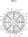
- Fig. 3 is a top view of the holding surface 7a that is the top surface of the stage 7.
- Fig. 4 is a vertical cross sectional view showing an upper portion of the stage 7 which is taken along line IV-IV in Fig. 3 .
- Fig. 5 is an enlarged view of A part surrounded by a dashed line in Fig. 4 .
- the vacuum chuck mechanism 60 includes suction grooves 7b formed in the holding surface 7a of the stage 7, a suction line 63 connected to the suction grooves 7b, and a vacuum pump 70 connected to the other end of the suction line 63.
- the fine suction grooves 7b for sucking the wafer W are formed in the holding surface 7a of the stage 7.
- the suction grooves 7b are indicated by lines.
- the suction grooves 7b are recesses formed in the holding surface 7a of the stage 7.
- the suction grooves 7b are connected to the vacuum pump 70 through the suction line 63. In a state where the wafer W is held on the holding surface 7a, the suction grooves 7b are sealed by the wafer W and a pressure in the grooves is maintained in a depressurized state.
- the suction grooves 7b are divided into a plurality of suction regions 61.
- the suction grooves 7b are divided into nine suction regions 61A, 61B, 61C, 61D, 61E, 61F, 61G, 61H and 61I which can be separately maintained in a depressurized state.
- the suction region 61I is a central region provided at a central portion of the holding surface 7a having a circular shape when seen from the top.
- the suction regions 61A, 61B, 61C, 61D, 61E, 61F, 61G and 61H are outer peripheral regions provided around the suction region 61I on the holding surface 7a having a circular shape when seen from the top.
- the suction region 61I sucks the central portion of the circular wafer W.
- the suction regions 61A, 61B, 61C, 61D, 61E, 61F, 61G and 61H suck the peripheral portion of the circular wafer W.
- the suction grooves 7b are formed in a predetermined pattern.
- the suction grooves 7b communicate with each other in the respective suction regions 61A to 61I.
- the suction grooves 7b do not communicate with each other between different suction regions.
- Fig. 6 shows a connection state between the vacuum pump 70 and the suction regions 61A to 61I in the vacuum chuck mechanism 60.
- the suction grooves 7b in the respective suction regions 61A to 611 are connected to the vacuum pump 70 through lines 63A to 63I each forming a part of the suction line 63.
- Switching valves 65A to 65I are provided in the respective lines 63A to 63I.
- the switching valves 65A to 65I perform switching between a state in which the suction regions 61A to 61I can be sucked by the vacuum pump 70 and a state in which the suction regions 61A to 61I are exposed to external air 71 through gas exhaust lines 67A to 67I.
- each of the suction regions 61A to 611 can suck the wafer W partially.
- the suction region 61A and the suction region 61B can separately have a suction state and a non-suction state for the wafer W.
- the suction state and the non-suction state of the respective suction regions 61A to 61I can be controlled separately, even if the wafer W that is likely to warp considerably has portions where the suction is insufficient, it is possible to reliably attract and hold the wafer W at other portions. Accordingly, the misalignment of the wafer W during the probe inspection can be prevented.
- a vacuum gauge 73 is provided in the suction line 63. By measuring a pressure in the suction line 63 by the vacuum gauge 73, it is possible to detect whether or not leakage in which external air enters occurs at any one of the suction regions 61A to 611.
- the vacuum gauge 73 may be provided for each of the suction regions 61A to 61I, not for all the suction regions 61A to 61I. Or, the suction regions 61A to 61I may be divided into a plurality of groups and the vacuum gauge 73 may be provided for each group.
- the holding surface 7a is divided into the nine suction regions 61A to 61I.
- the number of the suction regions is not limited to nine.
- the holding surface 7a may be divided into a plurality of fanwise-shaped suction regions 61 arranged along the circumferential direction without being divided into a central portion and a peripheral portion.
- the suction region 61 is divided into the central portion and the peripheral portion of the holding surface 7a.
- the peripheral portion is preferably divided into at least four suction regions 61, more preferably 4 to 12 suction regions 61, and further more preferably 4 to 8 suction regions 61.
- the suction regions 61A to 61I may be divided into a plurality of groups.
- the suction regions 61A and 61B may be set to one group; the suction regions 61C and 61D may be set to one group; the suction regions 61E and 61F may be set to one group; and the suction regions 61G and 61H may be set to one group.
- the suction state and the non-suction state may be switched on a group basis.
- the gas ejection unit 45 includes: a plurality of (e.g., three) nozzles 81 for ejecting a gas toward the top surface of the wafer W locally; a nozzle plate 83 for holding the nozzles 81; a line 65 for supplying the gas to the respective nozzles 81 while being connected to the respective nozzles 81; and a gas source 87 connected to the other end of the line 85.
- a plurality of (e.g., three) nozzles 81 for ejecting a gas toward the top surface of the wafer W locally
- a nozzle plate 83 for holding the nozzles 81
- a line 65 for supplying the gas to the respective nozzles 81 while being connected to the respective nozzles 81
- a gas source 87 connected to the other end of the line 85.
- a mass flow controller MFC for controlling a flow rate and an opening/closing valve 91 are provided in the line 85.
- the gas it is possible to use, e.g., dry air, nitrogen gas, rare gas or the like.
- the nozzles 81 are connected to the gas source 87 through branch lines 85A to 85C of the line 85, respectively.
- the branch lines 85A to 85C are provided with opening/closing valves 93A to 93C, respectively.
- a heating gas may be used as the gas ejected from the gas ejection unit 45.
- a temperature of the heating gas is preferably the same as that of the holding surface 7a.
- the temperature of the heating gas is preferably set within a range of ⁇ 10°C with respect to the temperature of the holding surface 7a of the stage 7 and more preferably set within a range of ⁇ 5°C with respect to the temperature of the holding surface 7a of the stage 7.
- the temperature of the heating gas is preferably within a range from 110°C to 130°C and more preferably within a range from 115°C to 125°C.
- the temperature of the heating gas is preferably within a range from 140°C to 160°C and more preferably within a range from 145°C to 155°C.
- the wafer W can be heated from the top surface side thereof. Accordingly, a temperature difference between the top surface and the backside of the wafer W mounted on the holding surface 7a of the stage 7 can be minimized and, thus, it is possible to suppress warpage of the wafer W during the heating.
- the wafer W has a laminated structure of different resins, the wafer W is easily warped due to a difference in thermal expansion coefficients between materials. Therefore, it is effective to use the heating gas to suppress the warpage of the wafer W.
- the wafer W can be heated from the top surface side by the heating gas, the wafer W made of a thermoplastic resin has improved flexibility. As a result, the suction of the wafer W by the holding surface 7a of the stage 7 becomes easier.
- the nozzle plate 83 is held by the alignment unit 41. Therefore, the three nozzles 81 can move in the Y direction in Fig. 1 .
- the stage 7 can move in the X-Y-Z direction in Fig. 1 by the X direction moving unit 21, the Y direction moving unit 23 and the Z direction moving unit 25. Accordingly, the gas can be ejected from the respective nozzles 81 separately toward target portions of the wafer W held by the stage 7.
- the gas can be ejected at different timings toward the nine suction regions 61A to 61I divided on the holding surface 7a of the stage 7. For example, in Fig.
- gas ejection positions 61A1, 61B1, 61C1, 61D1, 61E1, 61F1, 61G1, 61H1 and 61I1 are indicated by virtual lines on the nine suction regions 61A to 611. Therefore, the gas is ejected to each of nine positions on the wafer W held on the stage 7 which correspond to the suction regions 61A to 611.
- the number of the nozzles 81 is not limited to three and may be, e.g., one, two, or four or more.
- Nine nozzles 81 may be provided to correspond to the respective suction regions 61A to 61I.
- the gas ejection unit 45 and the alignment unit 41 may be provided independently.
- Fig. 8 shows a configuration example in which the nozzle plate 83 is supported by an independent supporting portion.
- the gas ejection unit 45A includes: a plurality of (e.g., three) nozzles 81 for ejecting a gas toward the top surface of the wafer W locally; a nozzle plate 83 for holding the respective nozzles 81; a line 85 for supplying a gas into the respective nozzles 81 while being connected to the respective nozzles 81; a gas source 87 connected to the other end of the line 85; a nozzle arm 95 for holding the nozzle plate 83; and a column 97 for supporting the nozzle arm 95.
- a plurality of (e.g., three) nozzles 81 for ejecting a gas toward the top surface of the wafer W locally
- a nozzle plate 83 for holding the respective nozzles 81
- a line 85 for supplying a gas into
- the nozzle arm 95 is configured to be extensible/contractible, rotatable and vertically movable in the X-Y-Z direction by a driving unit (not shown). By moving the nozzle arm 95 to a position directly above the wafer W held on the holding surface 7a of the stage 7, the gas can be ejected to a predetermined portion on the wafer W.
- a control unit 50 controls operations of the respective components of the probe apparatus 100.
- the control unit 50 is typically a computer.
- Fig. 9 shows an example of a hardware configuration of the control unit 50.
- the control unit 50 includes: a main controller 201; an input device 202 such as a keyboard, a mouse or the like; an output device 203 such as a printer or the like; a display device 204; a storage device 205; an external interface 206; and a bus 207 for connecting these components.
- the main controller 201 has a CPU (central processing unit) 211, a RAM (random access memory) 212 and a ROM (read-only memory) 213. Types of the storage device 205 may vary as long as information can be stored.
- the storage device 205 may be, e.g., a hard disk device or an optical disk device. Further, the storage device 205 stores information in a computer-readable recording medium 215 and reads out the information from the recording medium. Types of the recording medium 215 may vary as long as information can be stored.
- the recording medium 215 may be, e.g., a hard disk, an optical disk, a flash memory or the like.
- the recording medium 215 may store a recipe of a probe method performed in the probe apparatus 100 of the present embodiment.
- the control unit 50 controls the probe apparatus 100 of the present embodiment to inspect devices formed on a plurality of wafers W. Specifically, the control unit 50 controls the respective components of the probe apparatus 100 (e.g., a driving device such as the motor 23b or the like, a position detecting device such as the encoder 23c or the like, the lower image pickup unit 35, the upper image pickup unit 43, the gas ejection unit 45, the vacuum chuck mechanism 60 and the like), which is realized by allowing the CPU 211 to execute software (program) stored in the ROM 213 or the storage device 205 by using the RAM 212 as a work area.
- a driving device such as the motor 23b or the like
- a position detecting device such as the encoder 23c or the like
- the lower image pickup unit 35 the upper image pickup unit 43
- the gas ejection unit 45 the vacuum chuck mechanism 60 and the like
- the electrodes of the devices and the probe needles are brought into contact with each other by controlling a relative position between the wafer W held on the stage 7 and the probe card by moving the stage 7 in the horizontal direction (X direction, Y direction, ⁇ direction) and in the vertical direction (Z direction).
- the test head 5 allows an inspection current to flow to the device through the probe needles of the probe card.
- the probe card transmits an electrical signal indicating electrical characteristics of the devices to the test head 5.
- the test head 5 stores the transmitted electrical signal as measurement data and determines whether or not the device as an inspection target has electrical defects.
- a method for holding a wafer W will be described.
- relation between the suction regions 61A to 61I of the holding surface 7a of the stage 7 and portions of the wafer W which are sucked by the suction regions 61A to 611 will be described with reference to Fig. 10 .
- a portion of the wafer W which is sucked by the suction region 61A of the stage 7 is referred to as a section P A .
- a portion of the wafer W which is sucked by the suction region 61B is referred to as a section P B ; a portion of the wafer W which is sucked by the suction region 61C is referred to as a section P C ; a portion of the wafer W which is sucked by the suction region 61D is referred to as a section P D ; a portion of the wafer W which is sucked by the suction region 61E is referred to as a section P E ; a portion of the wafer W which is sucked by the suction region 61F is referred to as a section P F ; a portion of the wafer W which is sucked by the suction region 61G is referred to as a section P G ; a portion of the wafer W which is sucked by the suction region 61H is referred to as a section P H ; and a portion of the wafer W which is sucked by the suction region 61
- Fig. 11 is a flowchart for explaining an example of a sequence of the method for holding the wafer W according to the embodiment. This sequence includes processes from a step S1 to a step S10. First, as a preparation step, the wafer W is mounted on the holding surface 7a of the stage 7 by a transfer unit (not shown).
- a step S1 the section P I that is a central portion of the wafer W is sucked by the suction region 611.
- any one of the nozzles 81 in the gas ejection unit 45 is moved to a position directly above the section P I of the wafer W.
- the vacuum pump 70 is driven while a gas is ejected from the nozzle 81 toward the section P I of the wafer W.
- the suction groove 7b in the suction region 61I is set to a negative pressure by switching the switching valve 651.
- the suction grooves 7b in the suction regions 61A to 61H are exposed to the atmosphere.
- the section P I that is the central portion of the wafer W is sucked by the suction region 61I positioned therebelow due to a negative pressure at the backside of the wafer W while being assisted by a pressure of the gas ejected from the top.
- a step S2 the section P A in the peripheral portion which is adjacent to the section P I of the wafer W is sucked by the suction region 61A of the stage 7.
- any one of the nozzles 81 in the gas ejection unit 45 is moved to a position directly above the section P A of the wafer W.
- the gas is ejected from the nozzle 81 toward the section P A of the wafer W and the suction groove 7b in the suction region 61A is set to a negative pressure by switching the switching valve 65A.
- the suction grooves 7b in the suction regions 61B to 61H are exposed to the atmosphere.
- the suction groove 7b in the suction region 61I is maintained at the negative pressure as in the step S1.
- the section P A in the peripheral portion of the wafer W is sucked by the suction region 61A positioned therebelow due to a negative pressure at the backside of the wafer W while being assisted by a pressure of the gas ejected from the top.
- a step S3 the section P B in the peripheral portion which is adjacent to the section P A of the wafer W is sucked by the suction region 61B of the stage 7.
- Specific sequences are the same as those in the step S2 except that the gas is ejected from the nozzle 81 moved to a position directly above the section P B of the wafer W and the suction groove 7b in the suction region 61B is set to a negative pressure by switching the switching valve 65B.
- steps S4 to S9 a section in the peripheral portion which is adjacent to the section of the wafer W which is sucked in a previous step is sucked by the suction region of the stage 7 in the order of the suction regions 61C, 61D, 61E, 61F, 61G and 61H.
- step S10 it is possible to determine whether or not leakage has occurred in any of the suction regions 61A to 61I by measuring a pressure in the suction line 63 by the vacuum gauge 73 and comparing the measured pressure with a previously measured pressure in the suction line 63 in a normal attraction/holding state.
- the processing returns to the step S1 as indicated by a dashed line in Fig. 11 and the processes from the steps S1 to S9 are performed.
- the leakage detection is collectively performed for all the suction regions 61A to 61I.
- the leakage detection may be performed for each of the suction regions 61A to 61I by providing the vacuum gauge 73 for each of the lines 63A to 63I, for example.
- the leakage detection may be performed in each of the steps S1 to S9.
- the suction regions 61A to 6AI is divided into a plurality of groups and the leakage detection may be performed on a group basis.
- the suction process may be performed only for a region where the leakage has been detected among the suction regions 61A to 61I or only for a group where the leakage has been detected.
- the leakage detection in the step S10 is not necessary and may be omitted.
- the entire wafer W can be easily attracted and held on the holding surface 7a of the stage 7 by repeating the operation of ejecting the gas to the wafer W locally and allowing the wafer W to be partially sucked by the suction regions 61A to 61I.
- a section in the peripheral portion of the wafer W which is adjacent to the previously sucked section is sequentially sucked by the suction regions 61A to 61H while using a gas pressure. Therefore, even if the wafer W is warped considerably, for example, the wafer W can be reliably attracted and held on the holding surface 7a. Accordingly, the probe apparatus 100 can inspect the devices with high reliability.
- Fig. 12 is a flowchart for explaining another example of the sequence of the method for holding the wafer W according to the embodiment. This sequence includes processes from steps S11 to S17.
- the wafer W is mounted on the holding surface 7a of the stage 7 by a transfer unit (not shown).
- a step S11 the section P I as the central portion of the wafer W is sucked by the suction region 611.
- the step S11 may be executed in the same manner as that in the step S1 of the first sequence.
- a step S12 the section P A in the peripheral portion which is adjacent to the section P I of the wafer W is sucked by the suction region 61A of the stage 7.
- one of the nozzles 81 in the gas ejection unit 45 is moved to a position directly above the section P A of the wafer W.
- the gas is ejected from the nozzle 81 toward the section P A of the wafer W and the suction groove 7b in the suction region 61A is set to a negative pressure by switching the switching valve 65A.
- the suction grooves 7b in the suction regions 61B to 61H are exposed to the atmosphere.
- the suction groove 7b in the suction region 61I is maintained at the negative pressure as in the step S11.
- the section P A in the peripheral portion of the wafer W is sucked by the suction region 61A positioned therebelow due to a negative pressure at the backside of the wafer W while being assisted by a pressure of the gas ejected from the top.
- a step S13 two sections P B and P H in the peripheral portion which are adjacent to the section P A of the wafer W are sucked by the suction regions 61B and 61H of the stage 7, respectively.
- Specific sequences are the same as those in the step S12 except that the gas is ejected from two nozzles 81 moved to positions directly above the sections P B and P H of the wafer W toward the respective portions at the same time and the suction grooves 7b in the suction regions 61B and 61H are set to the negative pressure at the same time by switching the switching valves 65B and 65H.
- a step S14 two sections P C and P G in the peripheral portion which are adjacent to the sections P B and P H of the wafer W are sucked by the suction regions 61C and 61G of the stage 7, respectively.
- Specific sequences are the same as those in the step S12 except that the gas is ejected from two nozzles 81 moved to positions directly above the sections P C and P G of the wafer W toward the respective portions at the same time and the suction grooves 7b in the suction regions 61C and 61G are set to the negative pressure at the same time by switching the switching valves 65C and 65G.
- a step S15 two sections P D and P F in the peripheral portion which are adjacent to the sections P C and P G of the wafer W are sucked by the suction regions 61D and 61F of the stage 7, respectively.
- Specific sequences are the same as those in the step S12 except that the gas is ejected from two nozzles 81 moved to positions directly above the sections P D and P F of the wafer W toward the respective portions at the same time and the suction grooves 7b in the suction regions 61D and 61F are set to the negative pressure at the same time by switching the switching valves 65D and 65F.
- a section P E in the peripheral portion which is adjacent to the sections P D and P F of the wafer W is sucked by the suction region 61E of the stage 7.
- Specific sequences are the same as those in the step S12 except that the gas is ejected from the nozzle 81 moved to a position directly above the section P E of the wafer W and the suction groove 7b in the suction region 61E is set to the negative pressure by switching the switching valve 65E.
- step S17 When a normal state is obtained after the steps S11 to S16, the wafer W can be sucked by the entire holding surface 7a of the stage 7. However, when the wafer W is warped considerably, external air enters the suction groove 7b in any one of the suction regions 61A to 61I and leakage occurs, which may result in incomplete holding of the wafer W. Therefore, in this sequence, leakage detection is performed in a step S17. The leakage detection is performed in the same manner as that in the step S10 of the first sequence. When it is determined in the step S17 that the leakage has occurred, the processing returns to the step S11 as indicated by a dashed line in Fig. 12 and the processes from the steps S11 to S16 are performed.
- the leakage detection is collectively performed for all the suction regions 61A to 611.
- the leakage detection may be performed for each of the suction regions 61A to 61I by providing the vacuum gauge 73 for each of the lines 63A to 63I, for example.
- the leakage detection may be performed in each of the steps S11 to S16.
- the suction regions 61A to 6AI is divided into a plurality of groups and the leakage detection may be performed on a group basis.
- the suction process may be performed only for a region where the leakage has been detected among the suction regions 61A to 61I or only for a group where the leakage has been detected.
- the leakage detection in the step S17 is not necessary and may be omitted.
- Fig. 13 is a flowchart for explaining still another example of the method for holding the wafer W according to the embodiment. This sequence includes processes from steps S21 to S25.
- the wafer W is mounted on the holding surface 7a of the stage 7 by a transfer unit (not shown).
- a section P I that is a central portion of the wafer W is sucked by the suction region 61I.
- the step S21 may be executed in the same manner as that in the step S1 of the first sequence.
- a section P A in the peripheral portion of the wafer W which is adjacent to the section P I and a section P E positioned diametrically symmetrical to the section P A are sucked by the suction regions 61A and 61E of the stage 7, respectively.
- one of the nozzles 81 in the gas ejection unit 45 is moved to a position directly above the sections P A and P E of the wafer W.
- the gas is ejected from the nozzle 81 toward the sections P A and P E of the wafer W and the suction grooves in the suction regions 61A and 61E are set to the negative pressure at the same time by switching the switching valves 65A and 65E.
- the suction grooves 7b in the suction regions 61B to 61D and 61F to 61H are exposed to the atmosphere.
- the suction groove 7b in the suction region 611 is maintained at the negative pressure as in the step S21.
- the sections P A and P E in the peripheral portion of the wafer W are sucked by the suction regions 61A and 61E positioned therebelow due to a negative pressure at the backside of the wafer W while being assisted by a pressure of the gas ejected from the top.
- a step S23 two sections P B and P H in the peripheral portion which are adjacent to the section P A of the wafer W are sucked by the suction regions 61B and 61H of the stage 7, respectively.
- two sections P D and P F in the peripheral portion which are adjacent to the section P E of the wafer W are sucked by the suction regions 61D and 61F, respectively.
- a step S24 two remaining sections P C and P G in the peripheral portion of the wafer W are sucked by the suction regions 61C and 61G of the stage 7, respectively.
- Specific sequences are the same as those in the step S22 except that the gas is ejected from two nozzles 81 moved to positions directly above the sections P C and P G of the wafer W toward the respective portions at the same time and the suction grooves 7b in the suction regions 61C and 61G are set to the negative pressure at the same time by switching the switching valves 65C and 65G.
- step S25 When a normal state is obtained after the steps S21 to S24, the wafer W can be sucked by the entire holding surface 7a of the stage 7. However, when the wafer W is warped considerably, external air enters the suction groove 7b in any one of the suction regions 61A to 61I and leakage occurs, which may result in incomplete holding of the wafer W. Therefore, in this sequence, leakage check is performed in a step S25. The leakage check is performed in the same manner as that in the step S10 of the first sequence. When it is determined in the step S25 that the leakage has occurred, the processing returns to the step S21 as indicated by a dashed line in Fig. 13 and the processes from the steps S21 to S24 are performed.
- the leakage check is performed for all the suction regions 61A to 61I.
- the leakage check may be performed for each of the suction regions 61A to 61I by providing the vacuum gauge 73 for each of the lines 63A to 63I, for example.
- the leakage check may be performed in each of the steps S21 to S24.
- the suction regions 61A to 6AI is divided into a plurality of groups and the leakage check may be performed on a group basis.
- the suction process may be performed only for a region where the leakage has been detected among the suction regions 61A to 61I or only for a group where the leakage has been detected.
- the leakage check in the step S25 is optional and may be omitted.
- Fig. 3 shows the case in which eight suction regions 61A to 61H that suck the peripheral portion of the wafer W have the same shape and the same area.
- the suction regions 61 may have different areas or different shapes.
- modifications in which the suction regions 61 have different areas or different shapes will be described.
- Figs. 14 to 16 Modifications of the method for holding the wafer W according to the embodiment will be described with reference to Figs. 14 to 16 .
- the suction grooves 7b are not illustrated, and locations, shapes and areas of the suction regions 61 on the holding surface 7a of the stage 7 are schematically illustrated.
- the gas needs to be ejected from any one of the nozzles 81 in the gas ejection unit 45 during the suction operation.
- the leakage detection may be performed in the modifications.
- the holding surface 7a of the stage 7 is divided into seven suction regions 61A, 61B, 61C, 61D, 61E, 61F and 61G by the suction grooves 7b that can be maintained in a depressurized state separately.
- the suction region 61G is a central region provided at the central portion of the holding surface 7a having a circular shape when seen from the top.
- the suction regions 61A, 61B, 61C, 61D, 61E and 61F are peripheral regions provided around the suction region 61G on the holding surface 7a having the circular shape when seen from the top.
- the suction regions 61A to 61F include regions having different areas.
- the suction regions 61A and 61B have the same area and the suction regions 61C and 61D have the same area. However, the suction regions 61C and 6D are greater than the suction regions 61A and 61B.
- the suction region 61E is greater than the suction regions 61C and 61D.
- the suction region 61F is greater than the suction region 61E.
- the central portion of the wafer W is sucked by the suction region 61G and, then, the peripheral portion of the wafer W is partially and sequentially sucked by the suction regions 61A to 61F from the smallest area to the largest area. Specifically, a section in the peripheral portion of the wafer W is sucked by the suction region 61A. Next, a section in the peripheral portion of the wafer W, which is adjacent to the section sucked by the suction region 61A, is sucked by the suction region 61B.
- a section in the peripheral portion of the wafer W, which is adjacent to the portion sucked by the suction region 61D is sucked by the suction region 61E.
- the holding surface 7a of the stage 7 is divided into six suction regions 61A, 61B, 61C, 61D, 61E and 61H by the suction grooves 7b that can be maintained in a depressurized state separately.
- the suction region 61F is a central region provided at the central portion of the holding surface 7a having a circular shape when seen from the top.
- the suction regions 61A, 61B, 61C, 61D and 61E are peripheral regions provided around the suction region 61F on the holding surface 7a having the circular shape when seen from the top.
- the suction regions 61A to 61E include regions having different areas.
- the suction region 61A has the smallest area.
- the suction regions 61B and 61E have the same area.
- the suction regions 61B and 6E are greater than the suction region 61A.
- the suction regions 61C and 61D have the same area.
- the suction regions 61C and 61D are greater than the suction regions 61B and 61E.
- the central portion of the wafer W is sucked by the suction region 61F and, then, the peripheral portion of the wafer W is partially and sequentially sucked by the suction regions 61A to 61E from the smallest area to the largest area. Specifically, a section in the peripheral portion of the wafer W is sucked by the suction region 61A. Next, sections in the peripheral portion of the wafer W, which are adjacent to the section sucked by the suction region 61A, are sucked by the suction regions 61B and 61E.
- the holding surface 7a of the stage 7 is divided into nine suction regions 61A, 61B, 61C, 61D, 61E, 61F, 61G, 61H and 61I by the suction grooves 7b that can be maintained in a depressurized state separately.
- the suction region 611 is a central region provided at the central portion of the holding surface 7a having a circular shape when seen from the top.
- the suction regions 61A, 61B, 61C, 61D, 61E, 61F, 61G and 61H are peripheral regions provided around the suction region 61I on the holding surface 7a having the circular shape when seen from the top.
- the suction regions 61A to 61H include regions having different areas. Specifically, the suction regions 61A and 61B have the same area.
- the suction regions 61A and 61B are smallest regions in the peripheral region of the holding surface 7a of the stage 7 which are disposed at a radially inner side.
- the suction regions 61C and 61D have the same area.
- the suction regions 61C and 61D are greater than the suction regions 61A and 61B.
- the suction regions 61C and 61D are disposed at a radially outer side of the suction regions 61A and 61B in the peripheral region of the holding surface 7a of the stage 7.
- the suction regions 61E and 61H have the same area.
- the suction regions 61E and 61H are greater than the suction regions 61C and 61D.
- the suction regions 61F and 61G have the same area.
- the suction regions 61F and 61G are greater than the suction regions 61E and 61H.
- the central portion of the wafer W is sucked by the suction region 61I and, then, the peripheral portion of the wafer W is partially and sequentially sucked by the suction regions 61A to 61H from the smallest area to the largest area. Specifically, sections in the peripheral portion of the wafer W are sucked by the suction regions 61A and 61B. Next, sections in the peripheral portion of the wafer W, which are adjacent to the sections sucked by the suction regions 61A and 61B, are sucked by the suction regions 61C and 61D, respectively.
- a plurality of suction regions 61 for sucking the peripheral portion of the wafer W includes two or more suction regions 61 having different areas.
- the peripheral portion of the wafer W can be partially and sequentially sucked by the suction regions 61 from the smallest area to the largest area. Accordingly, even when the wafer W is warped considerably and only a smaller section thereof is sucked at first, the warpage of the wafer W can be gradually reduced by increasing the suction area by sequentially sucking sections adjacent thereto. As a result, the entire surface of the wafer W can be attracted and held on the entire holding surface 7a of the stage 7.
- the number of the suction regions 61 i.e., the number of divided portions of the holding surface 7a of the stage 7) can be reduced. Accordingly, the configuration of the apparatus can be simplified.
- Fig. 17 is a perspective view schematically showing an inner structure of a probe apparatus 100A according to the second embodiment.
- the probe apparatus 100A includes, as a pressing device, a pressing unit 101 for pressing the holding surface 7a of the stage 7 while being in contact with the top surface of the sucked portion of the wafer W.
- like reference numerals will designate like parts in the probe apparatus 100 according to the first embodiment, and redundant description thereof will be omitted.
- a plurality of pressing units 101 is provided at a side portion of the alignment unit 41.
- Figs. 18 and 19 explain one pressing unit.
- the pressing unit 101 has a pressing pin 103 as a pressing member, and a driving unit 105 for vertically displacing the pressing pin 103.
- a leading end of the pressing pin 103 is preferably made of a material having a thermal conductivity lower than that of a metal, such as ceramic, synthetic resin, rubber or the like, and more preferably made of a heat resistant elastic material such as fluorine rubber or the like.
- the driving unit 105 has an actuator such as an air cylinder or the like and a biasing member such as a spring or the like. As shown in Fig. 18 , a leading end of the pressing pin 103 is generally held at a retreat position higher than a lower end of the alignment unit 41 by a biasing force of the biasing member. When the actuator is driven, the pressing pin 103 moves downward by a predetermined stroke beyond the lower end of the alignment unit 41 against the biasing force of the biasing member and presses a part of the wafer W by the contact between the leading end of the pressing pin 103 and the top surface of the sucked portion of the wafer W, as can be seen from Fig. 19 .
- the pressing pin 103 functions in the same manner as the gas ejected from the gas ejection unit 45 in the first embodiment. In other words, the pressing pin 103 presses a part of the top surface of the wafer W against the holding surface 7a of the stage 7 positioned therebelow. As a result, in the probe apparatus 100A of the second embodiment, the wafer W can be attracted and held in the same manner as that in the probe apparatus 100 of the first embodiment.
- the number of the pressing units 101 is not limited to two, and may be one, or three or more. However, it is preferable to provide a plurality of pressing units 101.
- two pressing units 101 are provided at the side portion of the alignment unit 41 and can press the sucked portion of the wafer W. Accordingly, a moving distance of the stage 7 in the XY direction in the case of attracting and holding the wafer W is decreased, which makes it possible to reduce a foot print of the entire apparatus.
- an additional supporting mechanism is not required because the pressing units 101 are attached to the alignment unit 41. Therefore, the configuration of the apparatus can be simplified.
- the pressing units 101 may be supported by a separate supporting member instead of being attached to the alignment unit 41.
- the holding surface 7a of the stage 7 is divided into twelve suction regions 61 by the suction grooves 7b that can be maintained in a depressurized state separately.
- the twelve suction regions 61 partitioned on the holding surface 7a of the stage 7 are indicated by numbers 1 to 12 indicating the order of sucking the wafer W.
- the suction regions 61 indicated by numbers 1 and 2 are central regions provided at a central portion of the holding surface 7a having a circular shape when seen from the top.
- the suction regions indicated by the numbers 1 and 2 have different areas and are formed from the center of the holding surface 7a of the stage 7 toward a radially outer side.
- the central region may include a plurality of regions divided in a diametrical direction of the holding surface 7a.
- the suction regions 61 indicated by numbers 3 to 12 are peripheral regions formed around the central regions indicated by the numbers 1 and 2 on the holding surface 7a having a circular shape when seen from the top.
- the suction regions indicated by the numbers 3, 4 and 5 have different areas and are formed from the center side of the holding surface 7a of the stage 7 toward a radially outer side.
- the peripheral region may include a plurality of regions divided in a diametrical direction of the holding surface 7a.
- the central portion of the wafer W is sucked by the region of No. 1 and the region of No. 2 positioned at an outer side of the No. 1 region, which correspond to the central region of the holding surface 7a of the stage 7 in that order.
- the peripheral portion of the wafer W is sucked by the region of No. 3, the region of No. 4 and the region of No. 5, which correspond to the peripheral region of the holding surface 7a of the stage 7 in that order from the center side toward the diametrically outer side.
- the peripheral portion of the wafer W is sucked by the region of No. 6, the region of No. 7, the region of No. 8, the region of No.
- Figs. 21 to 33 the positional relation between the pressing pin 103 of the pressing unit 101 provided at two locations of the side portion of the alignment unit 41 and the holding surface 7a of the stage 7.
- the two pressing units 101 are distinguished by reference numerals 101A and 101B.
- Numbers 1 to 12 on the holding surface 7a of the stage 7 indicate the same as those in Fig. 20 .
- the wafer W itself is not illustrated.
- the alignment unit 41 can reciprocally move in the Y direction in the drawings and the stage 7 can move in the XY direction in the drawings.
- the stage 7 is moved to a delivery position of the wafer W. Then, the loader unit 3 transfers the wafer W (not shown) to the holding surface 7a of the stage 7.
- the alignment unit 41 is moved in the Y direction until the pressing pin 103 of the pressing unit 101A reaches a position directly above the region of No. 1.
- the suction of the No. 1 region is switched ON and the pressing pin 103 of the pressing unit 101A moves. Accordingly, the central portion of the wafer W is pressed and sucked by the region of No. 1.
- a pressing position of the pressing pin 103 is indicated by a black point (this holds true in Figs. 23 to 33 ).
- the suction state is checked through the leakage check and, then, the pressing pin 103 is retreated.
- the stage 7 is moved until the pressing pin 103 of the pressing unit 101A reaches a position directly above the region of No. 2.
- the suction of the No. 2 region is switched ON and the pressing pin 103 of the pressing unit 101A moves to press a radially outer side of the central portion of the wafer W, so that the wafer W is sucked by the No. 2 region.
- the suction state is checked through the leakage check and, then, the pressing pin 103 is retreated.
- the wafer W may be sucked by the No. 1 region and the No. 2 region in that order while maintaining a state in which one location at the central portion of the wafer W is pressed by the pressing pin 103 of the pressing unit 101A.
- the stage 7 is moved until the pressing pin 103 of the pressing unit 101A reaches a position directly above the region of No. 3.
- the suction of the No. 3 region is switched ON and the pressing pin 103 of the pressing unit 101A moves to press a part of the wafer W, so that the wafer W is sucked by the No. 3 region.
- the suction state is checked through the leakage check and, then, the pressing pin 103 is retreated.
- the stage 7 is moved until the pressing pin 103 of the pressing unit 101A reaches a position directly above the region of No. 4.
- the suction of the No. 4 region is switched ON and the pressing pin 103 of the pressing unit 101A moves to press a part of the wafer W, so that the wafer W is sucked by the No. 4 region.
- the suction state is checked through the leakage check and, then, the pressing pin 103 is retreated.
- the stage 7 is moved until the pressing pin 103 of the pressing unit 101A reaches a position directly above the 5 th region.
- the suction of the region of No. 5 is switched ON and the pressing pin 103 of the pressing unit 101A moves to press a part of the wafer W, so that the wafer W is sucked the no. 5 region.
- the suction state is checked through the leakage check and, then, the pressing pin 103 is retreated.
- the wafer W may be sucked by the No. 3 region, the No. 4 region and the No. 5 region in that order while maintaining a state in which one location on the wafer W corresponding to any one of the regions is pressed by the pressing pin 103 of the pressing unit 101A.
- the stage 7 is moved until the pressing pin 103 of the pressing unit 101A reaches a position directly above the region of No. 6.
- the suction of the No. 6 region is switched ON and the pressing pin 103 of the pressing unit 101A moves to press a part of the wafer W, so that the wafer W is sucked by the No. 6 region.
- the suction state is checked through the leakage check and, then, the pressing pin 103 is retreated.
- the wafer W is partially sucked while repeating the pressing and the retreat of the pressing pin 103 of the pressing unit 101A in the order of the region of No. 7 (see Fig. 28 ) and the region of No. 8 (see Fig. 29 ).
- the pressing unit 101B is replaced with the pressing unit 101A and the stage 7 is moved until the pressing pin 103 of the pressing unit 101B reaches a position directly above the region of No. 9.
- the suction of the No. 9 region is switched ON and the pressing pin 103 of the pressing unit 101A moves to press a part of the wafer W, so that the wafer W is sucked by the No. 9 region.
- the suction state is checked through the leakage check and, then, the pressing pin 103 is retreated.
- the wafer W is partially sucked by repeating the pressing and the retreat of the pressing pin 103 of the pressing unit 101B in the order of the region of No. 10 (see Fig. 31 ), the region of No. 11 (see Fig. 32 ) and the region of No. 12 (see Fig. 33 ).
- This sequence may be performed by repeating the start and the stop of gas ejection by providing the nozzle 81 of the gas ejection unit 45 of the first embodiment at two locations, instead of by repeating the pressing and the retreat of the pressing pin 103 of two pressing units 101 provided at the alignment unit 41.
- the present invention is not limited to the embodiments and may be variously modified.
- the probe apparatus for inspecting devices formed on the wafer W has been described.
- the substrate holding method and the substrate holding apparatus of the present invention can be applied to any processing apparatus including a stage for vacuum-attracting and holding a substrate.
- the section P I that is the central portion of the wafer W is sucked first.
- the suction region 61 is divided into a large number of portions, three or more sections in the peripheral portion of the wafer W may be sucked at the same time after the suction of the section P I .
- the substrate is not limited to a semiconductor wafer or a resin substrate.
- the substrate may be a glass substrate used in a flat panel display represented by a liquid crystal display, or an inspection substrate on which a plurality of IC (semiconductor integrated circuit) chips is mounted such as a resin substrate, a glass substrate or the like.
- IC semiconductor integrated circuit
Applications Claiming Priority (3)
| Application Number | Priority Date | Filing Date | Title |
|---|---|---|---|
| JP2015077278 | 2015-04-04 | ||
| JP2015229657A JP6568781B2 (ja) | 2015-04-04 | 2015-11-25 | 基板保持方法、基板保持装置、処理方法及び処理装置 |
| PCT/JP2016/053953 WO2016163147A1 (fr) | 2015-04-04 | 2016-02-10 | Procédé de maintien de substrat, dispositif de maintien de substrat, procédé de traitement et dispositif de traitement |
Publications (3)
| Publication Number | Publication Date |
|---|---|
| EP3282475A1 true EP3282475A1 (fr) | 2018-02-14 |
| EP3282475A4 EP3282475A4 (fr) | 2018-12-12 |
| EP3282475B1 EP3282475B1 (fr) | 2021-09-08 |
Family
ID=57358546
Family Applications (1)
| Application Number | Title | Priority Date | Filing Date |
|---|---|---|---|
| EP16776316.8A Active EP3282475B1 (fr) | 2015-04-04 | 2016-02-10 | Procédé de maintien de substrat, dispositif de maintien de substrat, procédé de traitement et dispositif de traitement |
Country Status (5)
| Country | Link |
|---|---|
| EP (1) | EP3282475B1 (fr) |
| JP (1) | JP6568781B2 (fr) |
| KR (1) | KR102044085B1 (fr) |
| CN (1) | CN107431039B (fr) |
| TW (1) | TWI681497B (fr) |
Families Citing this family (13)
| Publication number | Priority date | Publication date | Assignee | Title |
|---|---|---|---|---|
| JP6658491B2 (ja) * | 2016-12-15 | 2020-03-04 | 三菱電機株式会社 | ダイシング装置および半導体装置の製造方法 |
| JP6906980B2 (ja) * | 2017-02-27 | 2021-07-21 | 株式会社東京精密 | 研削装置 |
| JP6914078B2 (ja) * | 2017-03-31 | 2021-08-04 | 株式会社荏原製作所 | 真空吸着パッドおよび基板保持装置 |
| KR102397545B1 (ko) * | 2017-05-02 | 2022-05-12 | 삼성전자주식회사 | 척 스테이지 이물질 감지 장치 |
| EP3712929B1 (fr) * | 2017-11-17 | 2023-09-13 | Hamamatsu Photonics K.K. | Procédé d'aspiration |
| TW202401630A (zh) * | 2018-01-17 | 2024-01-01 | 日商東京威力科創股份有限公司 | 接合裝置及接合方法 |
| CN111615739A (zh) * | 2018-01-23 | 2020-09-01 | 东京毅力科创株式会社 | 基板处理装置、以及基板处理方法 |
| CN109746881A (zh) * | 2018-12-28 | 2019-05-14 | 深圳市华星光电半导体显示技术有限公司 | 基板载台 |
| JP2020145323A (ja) * | 2019-03-06 | 2020-09-10 | 東京エレクトロン株式会社 | 基板保持装置および基板吸着方法 |
| JP2022079225A (ja) | 2020-11-16 | 2022-05-26 | 東京エレクトロン株式会社 | 基板保持機構、基板載置方法及び基板離脱方法 |
| JP2022085481A (ja) | 2020-11-27 | 2022-06-08 | 東京エレクトロン株式会社 | 検査装置、チェンジキット、チェンジキットの交換方法 |
| TWI819623B (zh) * | 2022-05-24 | 2023-10-21 | 友威科技股份有限公司 | 電漿製程系統的載體吸附機構 |
| CN117798814A (zh) * | 2024-03-01 | 2024-04-02 | 浙江大学杭州国际科创中心 | 一种抛光垫、抛光垫的制备方法及抛光方法 |
Family Cites Families (13)
| Publication number | Priority date | Publication date | Assignee | Title |
|---|---|---|---|---|
| JP3105201B2 (ja) * | 1998-10-20 | 2000-10-30 | 株式会社東京精密 | ウェーハの搬送保持機構 |
| JP4283926B2 (ja) * | 1999-02-22 | 2009-06-24 | 株式会社アルバック | ウエハカセットのウエハ保持システム |
| KR20030042907A (ko) * | 2001-11-26 | 2003-06-02 | 삼성전자주식회사 | 웨이퍼 고정용 진공 장치 |
| JP4201564B2 (ja) * | 2001-12-03 | 2008-12-24 | 日東電工株式会社 | 半導体ウエハ搬送方法およびこれを用いた半導体ウエハ搬送装置 |
| JP5329191B2 (ja) * | 2008-11-27 | 2013-10-30 | 日置電機株式会社 | 吸着装置および検査装置 |
| JP2012201437A (ja) * | 2011-03-24 | 2012-10-22 | Tokyo Electron Ltd | 基板搬送装置及び基板搬送方法 |
| JP5877005B2 (ja) * | 2011-07-29 | 2016-03-02 | 株式会社Screenホールディングス | 基板処理装置、基板保持装置、および、基板保持方法 |
| JP2013120902A (ja) * | 2011-12-08 | 2013-06-17 | Tokyo Electron Ltd | 接合方法、プログラム、コンピュータ記憶媒体、接合装置及び接合システム |
| JP5913162B2 (ja) * | 2012-04-04 | 2016-04-27 | 東京エレクトロン株式会社 | 基板保持装置および基板保持方法 |
| JP5829171B2 (ja) | 2012-04-04 | 2015-12-09 | 東京エレクトロン株式会社 | 剥離システム、剥離方法、プログラム及びコンピュータ記憶媒体 |
| US8919528B2 (en) * | 2012-07-13 | 2014-12-30 | Hewlett-Packard Industrial Printing Ltd. | Nozzled device to align a substrate on a surface |
| JP2014195016A (ja) * | 2013-03-29 | 2014-10-09 | Sharp Corp | 半導体検査装置 |
| EP3051573A4 (fr) * | 2013-09-25 | 2017-05-03 | Shibaura Mechatronics Corporation | Étage d'aspiration, dispositif de liaison, et procédé de fabrication de substrat lié |
-
2015
- 2015-11-25 JP JP2015229657A patent/JP6568781B2/ja active Active
-
2016
- 2016-02-10 CN CN201680019629.8A patent/CN107431039B/zh active Active
- 2016-02-10 EP EP16776316.8A patent/EP3282475B1/fr active Active
- 2016-02-10 KR KR1020177031887A patent/KR102044085B1/ko active IP Right Grant
- 2016-03-29 TW TW105109853A patent/TWI681497B/zh active
Also Published As
| Publication number | Publication date |
|---|---|
| CN107431039A (zh) | 2017-12-01 |
| TW201703183A (zh) | 2017-01-16 |
| EP3282475A4 (fr) | 2018-12-12 |
| JP2016197707A (ja) | 2016-11-24 |
| JP6568781B2 (ja) | 2019-08-28 |
| CN107431039B (zh) | 2021-01-12 |
| KR102044085B1 (ko) | 2019-11-12 |
| TWI681497B (zh) | 2020-01-01 |
| EP3282475B1 (fr) | 2021-09-08 |
| KR20170135899A (ko) | 2017-12-08 |
Similar Documents
| Publication | Publication Date | Title |
|---|---|---|
| EP3282475B1 (fr) | Procédé de maintien de substrat, dispositif de maintien de substrat, procédé de traitement et dispositif de traitement | |
| EP3038146A1 (fr) | Élément auxiliaire de maintien de substrat et appareil de transfert de substrat | |
| US11099236B2 (en) | Inspection device and contact method | |
| JP5120018B2 (ja) | プローブ装置 | |
| JPH0883825A (ja) | プローブ装置 | |
| US10416228B2 (en) | Prober | |
| KR101335146B1 (ko) | 프로브 카드 검출 장치, 웨이퍼의 위치 정렬 장치 및 웨이퍼의 위치 정렬 방법 | |
| US11346861B2 (en) | Contact accuracy assurance method, contact accuracy assurance mechanism, and inspection apparatus | |
| JP3172760B2 (ja) | バキュームコンタクタ | |
| US7265536B2 (en) | Procedure for reproduction of a calibration position of an aligned and afterwards displaced calibration substrate in a probe station | |
| JP2018067603A (ja) | プローバ及びプローブ検査方法 | |
| KR20130018580A (ko) | 웨이퍼 반송 장치 | |
| US11169206B2 (en) | Inspection apparatus, inspection system, and aligning method | |
| JP7389945B2 (ja) | プローバ及びプローブ検査方法 | |
| JP6801166B2 (ja) | プローバ及びプローブ検査方法 | |
| JPH10223704A (ja) | ウエハの一括検査装置及びウエハの一括検査方法 | |
| JP2995134B2 (ja) | プローブ装置 | |
| JP7267058B2 (ja) | 検査装置 | |
| CN113508457A (zh) | 基片保持装置和基片吸附方法 | |
| KR20200104802A (ko) | 기판 처리 장치, 기판 처리 방법 및 접합 방법 | |
| US9726719B2 (en) | Semiconductor automatic test equipment | |
| WO2016163147A1 (fr) | Procédé de maintien de substrat, dispositif de maintien de substrat, procédé de traitement et dispositif de traitement | |
| JP7352812B2 (ja) | プローバ及びプローブ検査方法 | |
| JP4959669B2 (ja) | プローブ装置 | |
| JPH0794560A (ja) | プローブ装置 |
Legal Events
| Date | Code | Title | Description |
|---|---|---|---|
| STAA | Information on the status of an ep patent application or granted ep patent |
Free format text: STATUS: THE INTERNATIONAL PUBLICATION HAS BEEN MADE |
|
| PUAI | Public reference made under article 153(3) epc to a published international application that has entered the european phase |
Free format text: ORIGINAL CODE: 0009012 |
|
| STAA | Information on the status of an ep patent application or granted ep patent |
Free format text: STATUS: REQUEST FOR EXAMINATION WAS MADE |
|
| 17P | Request for examination filed |
Effective date: 20171102 |
|
| AK | Designated contracting states |
Kind code of ref document: A1 Designated state(s): AL AT BE BG CH CY CZ DE DK EE ES FI FR GB GR HR HU IE IS IT LI LT LU LV MC MK MT NL NO PL PT RO RS SE SI SK SM TR |
|
| AX | Request for extension of the european patent |
Extension state: BA ME |
|
| DAV | Request for validation of the european patent (deleted) | ||
| DAX | Request for extension of the european patent (deleted) | ||
| A4 | Supplementary search report drawn up and despatched |
Effective date: 20181112 |
|
| RIC1 | Information provided on ipc code assigned before grant |
Ipc: H01L 21/683 20060101AFI20181106BHEP |
|
| GRAP | Despatch of communication of intention to grant a patent |
Free format text: ORIGINAL CODE: EPIDOSNIGR1 |
|
| STAA | Information on the status of an ep patent application or granted ep patent |
Free format text: STATUS: GRANT OF PATENT IS INTENDED |
|
| INTG | Intention to grant announced |
Effective date: 20210512 |
|
| GRAS | Grant fee paid |
Free format text: ORIGINAL CODE: EPIDOSNIGR3 |
|
| GRAA | (expected) grant |
Free format text: ORIGINAL CODE: 0009210 |
|
| STAA | Information on the status of an ep patent application or granted ep patent |
Free format text: STATUS: THE PATENT HAS BEEN GRANTED |
|
| AK | Designated contracting states |
Kind code of ref document: B1 Designated state(s): AL AT BE BG CH CY CZ DE DK EE ES FI FR GB GR HR HU IE IS IT LI LT LU LV MC MK MT NL NO PL PT RO RS SE SI SK SM TR |
|
| REG | Reference to a national code |
Ref country code: GB Ref legal event code: FG4D |
|
| REG | Reference to a national code |
Ref country code: AT Ref legal event code: REF Ref document number: 1429339 Country of ref document: AT Kind code of ref document: T Effective date: 20210915 Ref country code: CH Ref legal event code: EP |
|
| REG | Reference to a national code |
Ref country code: IE Ref legal event code: FG4D |
|
| REG | Reference to a national code |
Ref country code: DE Ref legal event code: R096 Ref document number: 602016063465 Country of ref document: DE |
|
| REG | Reference to a national code |
Ref country code: LT Ref legal event code: MG9D |
|
| REG | Reference to a national code |
Ref country code: NL Ref legal event code: MP Effective date: 20210908 |
|
| PG25 | Lapsed in a contracting state [announced via postgrant information from national office to epo] |
Ref country code: RS Free format text: LAPSE BECAUSE OF FAILURE TO SUBMIT A TRANSLATION OF THE DESCRIPTION OR TO PAY THE FEE WITHIN THE PRESCRIBED TIME-LIMIT Effective date: 20210908 Ref country code: SE Free format text: LAPSE BECAUSE OF FAILURE TO SUBMIT A TRANSLATION OF THE DESCRIPTION OR TO PAY THE FEE WITHIN THE PRESCRIBED TIME-LIMIT Effective date: 20210908 Ref country code: LT Free format text: LAPSE BECAUSE OF FAILURE TO SUBMIT A TRANSLATION OF THE DESCRIPTION OR TO PAY THE FEE WITHIN THE PRESCRIBED TIME-LIMIT Effective date: 20210908 Ref country code: BG Free format text: LAPSE BECAUSE OF FAILURE TO SUBMIT A TRANSLATION OF THE DESCRIPTION OR TO PAY THE FEE WITHIN THE PRESCRIBED TIME-LIMIT Effective date: 20211208 Ref country code: NO Free format text: LAPSE BECAUSE OF FAILURE TO SUBMIT A TRANSLATION OF THE DESCRIPTION OR TO PAY THE FEE WITHIN THE PRESCRIBED TIME-LIMIT Effective date: 20211208 Ref country code: FI Free format text: LAPSE BECAUSE OF FAILURE TO SUBMIT A TRANSLATION OF THE DESCRIPTION OR TO PAY THE FEE WITHIN THE PRESCRIBED TIME-LIMIT Effective date: 20210908 Ref country code: ES Free format text: LAPSE BECAUSE OF FAILURE TO SUBMIT A TRANSLATION OF THE DESCRIPTION OR TO PAY THE FEE WITHIN THE PRESCRIBED TIME-LIMIT Effective date: 20210908 Ref country code: HR Free format text: LAPSE BECAUSE OF FAILURE TO SUBMIT A TRANSLATION OF THE DESCRIPTION OR TO PAY THE FEE WITHIN THE PRESCRIBED TIME-LIMIT Effective date: 20210908 |
|
| REG | Reference to a national code |
Ref country code: AT Ref legal event code: MK05 Ref document number: 1429339 Country of ref document: AT Kind code of ref document: T Effective date: 20210908 |
|
| PG25 | Lapsed in a contracting state [announced via postgrant information from national office to epo] |
Ref country code: LV Free format text: LAPSE BECAUSE OF FAILURE TO SUBMIT A TRANSLATION OF THE DESCRIPTION OR TO PAY THE FEE WITHIN THE PRESCRIBED TIME-LIMIT Effective date: 20210908 Ref country code: GR Free format text: LAPSE BECAUSE OF FAILURE TO SUBMIT A TRANSLATION OF THE DESCRIPTION OR TO PAY THE FEE WITHIN THE PRESCRIBED TIME-LIMIT Effective date: 20211209 |
|
| PG25 | Lapsed in a contracting state [announced via postgrant information from national office to epo] |
Ref country code: AT Free format text: LAPSE BECAUSE OF FAILURE TO SUBMIT A TRANSLATION OF THE DESCRIPTION OR TO PAY THE FEE WITHIN THE PRESCRIBED TIME-LIMIT Effective date: 20210908 |
|
| PG25 | Lapsed in a contracting state [announced via postgrant information from national office to epo] |
Ref country code: IS Free format text: LAPSE BECAUSE OF FAILURE TO SUBMIT A TRANSLATION OF THE DESCRIPTION OR TO PAY THE FEE WITHIN THE PRESCRIBED TIME-LIMIT Effective date: 20220108 Ref country code: SM Free format text: LAPSE BECAUSE OF FAILURE TO SUBMIT A TRANSLATION OF THE DESCRIPTION OR TO PAY THE FEE WITHIN THE PRESCRIBED TIME-LIMIT Effective date: 20210908 Ref country code: SK Free format text: LAPSE BECAUSE OF FAILURE TO SUBMIT A TRANSLATION OF THE DESCRIPTION OR TO PAY THE FEE WITHIN THE PRESCRIBED TIME-LIMIT Effective date: 20210908 Ref country code: RO Free format text: LAPSE BECAUSE OF FAILURE TO SUBMIT A TRANSLATION OF THE DESCRIPTION OR TO PAY THE FEE WITHIN THE PRESCRIBED TIME-LIMIT Effective date: 20210908 Ref country code: PT Free format text: LAPSE BECAUSE OF FAILURE TO SUBMIT A TRANSLATION OF THE DESCRIPTION OR TO PAY THE FEE WITHIN THE PRESCRIBED TIME-LIMIT Effective date: 20220110 Ref country code: PL Free format text: LAPSE BECAUSE OF FAILURE TO SUBMIT A TRANSLATION OF THE DESCRIPTION OR TO PAY THE FEE WITHIN THE PRESCRIBED TIME-LIMIT Effective date: 20210908 Ref country code: NL Free format text: LAPSE BECAUSE OF FAILURE TO SUBMIT A TRANSLATION OF THE DESCRIPTION OR TO PAY THE FEE WITHIN THE PRESCRIBED TIME-LIMIT Effective date: 20210908 Ref country code: EE Free format text: LAPSE BECAUSE OF FAILURE TO SUBMIT A TRANSLATION OF THE DESCRIPTION OR TO PAY THE FEE WITHIN THE PRESCRIBED TIME-LIMIT Effective date: 20210908 Ref country code: CZ Free format text: LAPSE BECAUSE OF FAILURE TO SUBMIT A TRANSLATION OF THE DESCRIPTION OR TO PAY THE FEE WITHIN THE PRESCRIBED TIME-LIMIT Effective date: 20210908 Ref country code: AL Free format text: LAPSE BECAUSE OF FAILURE TO SUBMIT A TRANSLATION OF THE DESCRIPTION OR TO PAY THE FEE WITHIN THE PRESCRIBED TIME-LIMIT Effective date: 20210908 |
|
| REG | Reference to a national code |
Ref country code: DE Ref legal event code: R097 Ref document number: 602016063465 Country of ref document: DE |
|
| PLBE | No opposition filed within time limit |
Free format text: ORIGINAL CODE: 0009261 |
|
| STAA | Information on the status of an ep patent application or granted ep patent |
Free format text: STATUS: NO OPPOSITION FILED WITHIN TIME LIMIT |
|
| PG25 | Lapsed in a contracting state [announced via postgrant information from national office to epo] |
Ref country code: DK Free format text: LAPSE BECAUSE OF FAILURE TO SUBMIT A TRANSLATION OF THE DESCRIPTION OR TO PAY THE FEE WITHIN THE PRESCRIBED TIME-LIMIT Effective date: 20210908 |
|
| 26N | No opposition filed |
Effective date: 20220609 |
|
| PG25 | Lapsed in a contracting state [announced via postgrant information from national office to epo] |
Ref country code: SI Free format text: LAPSE BECAUSE OF FAILURE TO SUBMIT A TRANSLATION OF THE DESCRIPTION OR TO PAY THE FEE WITHIN THE PRESCRIBED TIME-LIMIT Effective date: 20210908 |
|
| PG25 | Lapsed in a contracting state [announced via postgrant information from national office to epo] |
Ref country code: MC Free format text: LAPSE BECAUSE OF FAILURE TO SUBMIT A TRANSLATION OF THE DESCRIPTION OR TO PAY THE FEE WITHIN THE PRESCRIBED TIME-LIMIT Effective date: 20210908 |
|
| REG | Reference to a national code |
Ref country code: CH Ref legal event code: PL |
|
| REG | Reference to a national code |
Ref country code: BE Ref legal event code: MM Effective date: 20220228 |
|
| GBPC | Gb: european patent ceased through non-payment of renewal fee |
Effective date: 20220210 |
|
| PG25 | Lapsed in a contracting state [announced via postgrant information from national office to epo] |
Ref country code: LU Free format text: LAPSE BECAUSE OF NON-PAYMENT OF DUE FEES Effective date: 20220210 |
|
| PG25 | Lapsed in a contracting state [announced via postgrant information from national office to epo] |
Ref country code: FR Free format text: LAPSE BECAUSE OF NON-PAYMENT OF DUE FEES Effective date: 20220228 |
|
| PG25 | Lapsed in a contracting state [announced via postgrant information from national office to epo] |
Ref country code: LI Free format text: LAPSE BECAUSE OF NON-PAYMENT OF DUE FEES Effective date: 20220228 Ref country code: IT Free format text: LAPSE BECAUSE OF FAILURE TO SUBMIT A TRANSLATION OF THE DESCRIPTION OR TO PAY THE FEE WITHIN THE PRESCRIBED TIME-LIMIT Effective date: 20210908 Ref country code: IE Free format text: LAPSE BECAUSE OF NON-PAYMENT OF DUE FEES Effective date: 20220210 Ref country code: GB Free format text: LAPSE BECAUSE OF NON-PAYMENT OF DUE FEES Effective date: 20220210 Ref country code: CH Free format text: LAPSE BECAUSE OF NON-PAYMENT OF DUE FEES Effective date: 20220228 |
|
| PG25 | Lapsed in a contracting state [announced via postgrant information from national office to epo] |
Ref country code: BE Free format text: LAPSE BECAUSE OF NON-PAYMENT OF DUE FEES Effective date: 20220228 |
|
| PGFP | Annual fee paid to national office [announced via postgrant information from national office to epo] |
Ref country code: DE Payment date: 20221229 Year of fee payment: 8 |
|
| PG25 | Lapsed in a contracting state [announced via postgrant information from national office to epo] |
Ref country code: HU Free format text: LAPSE BECAUSE OF FAILURE TO SUBMIT A TRANSLATION OF THE DESCRIPTION OR TO PAY THE FEE WITHIN THE PRESCRIBED TIME-LIMIT; INVALID AB INITIO Effective date: 20160210 |
|
| PG25 | Lapsed in a contracting state [announced via postgrant information from national office to epo] |
Ref country code: MK Free format text: LAPSE BECAUSE OF FAILURE TO SUBMIT A TRANSLATION OF THE DESCRIPTION OR TO PAY THE FEE WITHIN THE PRESCRIBED TIME-LIMIT Effective date: 20210908 Ref country code: CY Free format text: LAPSE BECAUSE OF FAILURE TO SUBMIT A TRANSLATION OF THE DESCRIPTION OR TO PAY THE FEE WITHIN THE PRESCRIBED TIME-LIMIT Effective date: 20210908 |
|
| PGFP | Annual fee paid to national office [announced via postgrant information from national office to epo] |
Ref country code: DE Payment date: 20231228 Year of fee payment: 9 |