EP3231880B1 - Orientiertes kupferblech, kupferkaschiertes laminat, flexible leiterplatte und elektronische vorrichtung - Google Patents
Orientiertes kupferblech, kupferkaschiertes laminat, flexible leiterplatte und elektronische vorrichtung Download PDFInfo
- Publication number
- EP3231880B1 EP3231880B1 EP15866605.7A EP15866605A EP3231880B1 EP 3231880 B1 EP3231880 B1 EP 3231880B1 EP 15866605 A EP15866605 A EP 15866605A EP 3231880 B1 EP3231880 B1 EP 3231880B1
- Authority
- EP
- European Patent Office
- Prior art keywords
- copper
- copper plate
- mass
- circuit board
- oriented
- Prior art date
- Legal status (The legal status is an assumption and is not a legal conclusion. Google has not performed a legal analysis and makes no representation as to the accuracy of the status listed.)
- Active
Links
Images

Classifications
-
- H—ELECTRICITY
- H05—ELECTRIC TECHNIQUES NOT OTHERWISE PROVIDED FOR
- H05K—PRINTED CIRCUITS; CASINGS OR CONSTRUCTIONAL DETAILS OF ELECTRIC APPARATUS; MANUFACTURE OF ASSEMBLAGES OF ELECTRICAL COMPONENTS
- H05K1/00—Printed circuits
- H05K1/02—Details
- H05K1/09—Use of materials for the conductive, e.g. metallic pattern
-
- C—CHEMISTRY; METALLURGY
- C22—METALLURGY; FERROUS OR NON-FERROUS ALLOYS; TREATMENT OF ALLOYS OR NON-FERROUS METALS
- C22C—ALLOYS
- C22C9/00—Alloys based on copper
-
- C—CHEMISTRY; METALLURGY
- C22—METALLURGY; FERROUS OR NON-FERROUS ALLOYS; TREATMENT OF ALLOYS OR NON-FERROUS METALS
- C22F—CHANGING THE PHYSICAL STRUCTURE OF NON-FERROUS METALS AND NON-FERROUS ALLOYS
- C22F1/00—Changing the physical structure of non-ferrous metals or alloys by heat treatment or by hot or cold working
- C22F1/08—Changing the physical structure of non-ferrous metals or alloys by heat treatment or by hot or cold working of copper or alloys based thereon
-
- H—ELECTRICITY
- H01—ELECTRIC ELEMENTS
- H01B—CABLES; CONDUCTORS; INSULATORS; SELECTION OF MATERIALS FOR THEIR CONDUCTIVE, INSULATING OR DIELECTRIC PROPERTIES
- H01B1/00—Conductors or conductive bodies characterised by the conductive materials; Selection of materials as conductors
- H01B1/02—Conductors or conductive bodies characterised by the conductive materials; Selection of materials as conductors mainly consisting of metals or alloys
- H01B1/026—Alloys based on copper
-
- H—ELECTRICITY
- H01—ELECTRIC ELEMENTS
- H01B—CABLES; CONDUCTORS; INSULATORS; SELECTION OF MATERIALS FOR THEIR CONDUCTIVE, INSULATING OR DIELECTRIC PROPERTIES
- H01B5/00—Non-insulated conductors or conductive bodies characterised by their form
- H01B5/02—Single bars, rods, wires, or strips
-
- H—ELECTRICITY
- H05—ELECTRIC TECHNIQUES NOT OTHERWISE PROVIDED FOR
- H05K—PRINTED CIRCUITS; CASINGS OR CONSTRUCTIONAL DETAILS OF ELECTRIC APPARATUS; MANUFACTURE OF ASSEMBLAGES OF ELECTRICAL COMPONENTS
- H05K1/00—Printed circuits
- H05K1/02—Details
- H05K1/03—Use of materials for the substrate
- H05K1/05—Insulated conductive substrates, e.g. insulated metal substrate
-
- H—ELECTRICITY
- H05—ELECTRIC TECHNIQUES NOT OTHERWISE PROVIDED FOR
- H05K—PRINTED CIRCUITS; CASINGS OR CONSTRUCTIONAL DETAILS OF ELECTRIC APPARATUS; MANUFACTURE OF ASSEMBLAGES OF ELECTRICAL COMPONENTS
- H05K3/00—Apparatus or processes for manufacturing printed circuits
- H05K3/02—Apparatus or processes for manufacturing printed circuits in which the conductive material is applied to the surface of the insulating support and is thereafter removed from such areas of the surface which are not intended for current conducting or shielding
- H05K3/022—Processes for manufacturing precursors of printed circuits, i.e. copper-clad substrates
-
- H—ELECTRICITY
- H05—ELECTRIC TECHNIQUES NOT OTHERWISE PROVIDED FOR
- H05K—PRINTED CIRCUITS; CASINGS OR CONSTRUCTIONAL DETAILS OF ELECTRIC APPARATUS; MANUFACTURE OF ASSEMBLAGES OF ELECTRICAL COMPONENTS
- H05K3/00—Apparatus or processes for manufacturing printed circuits
- H05K3/02—Apparatus or processes for manufacturing printed circuits in which the conductive material is applied to the surface of the insulating support and is thereafter removed from such areas of the surface which are not intended for current conducting or shielding
- H05K3/06—Apparatus or processes for manufacturing printed circuits in which the conductive material is applied to the surface of the insulating support and is thereafter removed from such areas of the surface which are not intended for current conducting or shielding the conductive material being removed chemically or electrolytically, e.g. by photo-etch process
-
- H—ELECTRICITY
- H05—ELECTRIC TECHNIQUES NOT OTHERWISE PROVIDED FOR
- H05K—PRINTED CIRCUITS; CASINGS OR CONSTRUCTIONAL DETAILS OF ELECTRIC APPARATUS; MANUFACTURE OF ASSEMBLAGES OF ELECTRICAL COMPONENTS
- H05K3/00—Apparatus or processes for manufacturing printed circuits
- H05K3/38—Improvement of the adhesion between the insulating substrate and the metal
-
- C—CHEMISTRY; METALLURGY
- C22—METALLURGY; FERROUS OR NON-FERROUS ALLOYS; TREATMENT OF ALLOYS OR NON-FERROUS METALS
- C22F—CHANGING THE PHYSICAL STRUCTURE OF NON-FERROUS METALS AND NON-FERROUS ALLOYS
- C22F1/00—Changing the physical structure of non-ferrous metals or alloys by heat treatment or by hot or cold working
-
- H—ELECTRICITY
- H05—ELECTRIC TECHNIQUES NOT OTHERWISE PROVIDED FOR
- H05K—PRINTED CIRCUITS; CASINGS OR CONSTRUCTIONAL DETAILS OF ELECTRIC APPARATUS; MANUFACTURE OF ASSEMBLAGES OF ELECTRICAL COMPONENTS
- H05K1/00—Printed circuits
- H05K1/02—Details
- H05K1/03—Use of materials for the substrate
- H05K1/0393—Flexible materials
-
- H—ELECTRICITY
- H05—ELECTRIC TECHNIQUES NOT OTHERWISE PROVIDED FOR
- H05K—PRINTED CIRCUITS; CASINGS OR CONSTRUCTIONAL DETAILS OF ELECTRIC APPARATUS; MANUFACTURE OF ASSEMBLAGES OF ELECTRICAL COMPONENTS
- H05K2201/00—Indexing scheme relating to printed circuits covered by H05K1/00
- H05K2201/01—Dielectrics
- H05K2201/0137—Materials
- H05K2201/0154—Polyimide
-
- H—ELECTRICITY
- H05—ELECTRIC TECHNIQUES NOT OTHERWISE PROVIDED FOR
- H05K—PRINTED CIRCUITS; CASINGS OR CONSTRUCTIONAL DETAILS OF ELECTRIC APPARATUS; MANUFACTURE OF ASSEMBLAGES OF ELECTRICAL COMPONENTS
- H05K2201/00—Indexing scheme relating to printed circuits covered by H05K1/00
- H05K2201/03—Conductive materials
- H05K2201/0302—Properties and characteristics in general
- H05K2201/0317—Thin film conductor layer; Thin film passive component
-
- H—ELECTRICITY
- H05—ELECTRIC TECHNIQUES NOT OTHERWISE PROVIDED FOR
- H05K—PRINTED CIRCUITS; CASINGS OR CONSTRUCTIONAL DETAILS OF ELECTRIC APPARATUS; MANUFACTURE OF ASSEMBLAGES OF ELECTRICAL COMPONENTS
- H05K2201/00—Indexing scheme relating to printed circuits covered by H05K1/00
- H05K2201/03—Conductive materials
- H05K2201/0332—Structure of the conductor
- H05K2201/0335—Layered conductors or foils
- H05K2201/0355—Metal foils
Definitions
- the present invention relates to an oriented copper plate having high strength and high durability against thermal cycle and fatigue caused by bending or the like, a copper-clad laminate and a flexible circuit board using the oriented copper plate, and an electronic device equipped with the circuit board.
- the present invention relates to an oriented copper plate having durability against bending, with which a flexible circuit board having excellent flexibility can be obtained, a copper-clad laminate and a flexible circuit board using the oriented copper plate, and an electronic device equipped with the circuit board.
- a ⁇ 100 ⁇ 001> texture has a stable recrystallization orientation of relatively high purity copper, which is texture orientation that is relatively easy to develop.
- texture orientation that is relatively easy to develop.
- cube orientation is obtained, in which the ⁇ 100> orientation is aligned with the rolling direction (RD), the normal direction (ND), and the transverse direction (TD) which is orthogonal to RD and ND.
- a cube texture is formed on a material, in order to improve fatigue characteristics (Patent Literature 1 and 2) and reduce Young's modulus (Patent Literature 3) and yield strength (Patent Literature 4) for softening.
- strain is repeatedly loaded on a metal material that constitutes such flexible circuit board copper foil or rectangular copper wire for solar cell connection.
- a metal material that constitutes such flexible circuit board copper foil or rectangular copper wire for solar cell connection.
- strain is caused by bending at a hinge portion, a slide portion, or a folding portion of a mobile phone.
- heat strain is caused by a difference in the thermal expansion coefficient between silicon and copper.
- a cube texture is usually formed by using a stable recrystallization orientation of relatively high-purity copper. This suggests that the number of dislocations or grain boundaries that originally act to increase strength is small.
- changes in stacking-fault energy might cause the stable recrystallization orientation to vary or precipitates to inhibit grain growth, thereby inhibiting cube texture formation.
- a copper material having an advanced cube texture is limited in terms of types or concentrations of alloy elements added. In particular, no copper alloy with a highly advanced cube orientation, which contains elements at high concentrations that would promote precipitation, has been found.
- the ⁇ 100> main orientation may be in the rolling direction.
- the longitudinal direction of a rectangular copper wire for solar cell connection corresponds to the ⁇ 100> orientation
- the stress direction of a flexible circuit board corresponds to the ⁇ 100> orientation without specific intention.
- the orientation results in the smallest breaking elongation, among possible orientations. Therefore, a material having an advanced cube texture is excellent in terms of fatigue characteristics while the orientation which is most likely to be used (i.e., ⁇ 100>) is undesirable in terms of fatigue characteristics. For such reasons, it is desirable to improve strength and enhance breaking elongation when stress is applied to a copper material having a highly developed cube texture in the ⁇ 100> direction.
- WO 2013/021969 A1 discloses a rolled copper foil for a secondary battery collector.
- an object of the present invention is to newly establish an oriented copper plate not only having a highly developed cube texture but also having strength and breaking elongation greater than those of a conventional material having a similar texture.
- Another object of the present invention is to newly establish a flexible circuit board that is excellent in terms of folding flexibility with the use of the oriented copper plate.
- an oriented copper plate may be obtained that may have features of material texture regarding both advanced cube texture and Cr precipitation, thereby achieving strength and breaking elongation greater than those of a conventional copper material which has a similar cube texture density and having excellent folding flexibility.
- Such oriented copper plate may be used for a wide range of applications such as a wiring material and a circuit board material.
- the oriented copper plate of the present invention is a material having an advanced cube texture formed therein, which contains Cr precipitates dispersed therein. It is a copper material having strength and breaking elongation greater than those of a conventional copper material having a similar cube texture density by promoting Cr precipitation, in which an advanced cube texture is formed. Therefore, it is excellent in terms of folding flexibility and thus can be used for a wide range of applications such as a wiring material and a circuit board material.
- the cube texture density of the oriented copper plate of the present invention is characterized in that the area percentage of a preferred orientation region having an orientation difference of not more than 15° with respect to two axes orthogonal to each other, one of which is in the thickness direction of the oriented copper plate, and the other one of which is in a given in-plane direction of the oriented copper plate, is not less than 60.0%.
- the copper plate is composed of rolled steel.
- a given in-plane direction of the oriented copper plate is a direction orthogonal to the rolling direction upon final cold rolling in the plate.
- the thickness direction of the oriented copper plate is a direction orthogonal to a rolled surface. Note that as plate cutting is arbitrarily determined depending on product shape, material yield, or the like, one side of the plate is not necessarily in the rolling direction as long as the oriented copper plate has a ⁇ 100> main orientation in two in-plane directions orthogonal to each other.
- the oriented copper plate does not have a complete plate shape.
- it may be formed in a wire rod having an elongated tape shape via slitting or a complicated circuit shape via etching of a part of the plate surface.
- the normal direction of the oriented copper plate is not particularly limited and the oriented copper plate includes not only a plate material having a certain thickness but also a very thin material such as copper foil.
- the oriented copper plate includes not only a plate material having a certain thickness but also a very thin material such as copper foil.
- it needs to be a copper plate having a substantial thickness of not more than 3 mm.
- the thickness may be appropriately determined depending on applications of the copper plate.
- the typical thickness is preferably 5 ⁇ m to 18 ⁇ m.
- the typical thickness is preferably 100 ⁇ m to 500 ⁇ m.
- the typical thickness of a rectangular copper wire (inter connector) used as a solar cell wiring material is preferably 100 ⁇ m to 300 ⁇ m. Note that the lower limit of the thickness is substantially 3 ⁇ m in view of limitations to rolling processing or handling in the subsequent processes.
- the texture of the copper plate of the present invention can be measured and evaluated by electron backscattered diffraction (EBSD), which is widely used as a crystal orientation analysis technique.
- EBSD is a technique of irradiating the surface of a sample with an electron beam in a localized manner and analyzing a diffraction pattern generated as a result of backscattering diffraction so as to determine an orientation of diffraction points using a scanning electron microscope (SEM).
- SEM scanning electron microscope
- orientation information obtained by EBSD is three-dimensional information
- orientation information of the copper plate can be evaluated based on a polished face of an arbitrary cross-sectional surface.
- an oriented copper plate for example, the area of a polished face of a C cross-section surface orthogonal to the plate face is limited. Therefore, according to the present invention, it is a standard way to select a large region having a size of not less than 800 ⁇ m ⁇ 1600 ⁇ m for the texture of an in-plane cross-sectional surface of the copper plate which is orthogonal to the normal direction of the copper plate and conduct evaluation at intervals of not more than 4 ⁇ m within the region.
- the oriented copper plate of the present invention is a copper plate containing 0.03% by mass to 1.0% by mass of Cr, the remainder of which is composed of copper and inevitable impurities. It has the aforementioned texture and a structure in which a matrix having an advanced cube texture contains 4-nm to 52-nm Cr precipitates at 300 precipitates/ ⁇ m 3 to 12000 precipitates/ ⁇ m 3 .
- the precipitate size used herein refers to an equivalent circle diameter calculated based on the area of precipitates projected from one direction of the copper plate.
- a crystal texture is substantially defined as a highly oriented cube texture. Therefore, crystal grains that form a cube texture are coarse, and therefore a technique of increasing strength by refining crystal grains may not be employed.
- a technique of alloying for solid solution promotion or precipitation promotion may be employed, an advanced cube texture may not be formed when alloy elements are added to concentrations at which the action of enhancing solid solution or precipitation can be observed, since the stable orientation of recrystallization varies or precipitates inhibits grain growth by changes in stacking-fault energy.
- copper is mainly used as an electrical conducting material, when the contents of alloy elements in copper are increased, electric resistance is increased and such a copper may be inappropriate for such use.
- Cr can exhibit an action of promoting precipitation even at a relatively low concentration of not less than 0.03% by mass, thereby promoting precipitation in a copper plate having an advanced cube texture.
- any alloy elements capable of promoting copper precipitation are known, only Cr has been found as an alloy element that can achieve both copper precipitation and advanced cube texture formation.
- the Cr concentration is not more than 1.0% by mass and desirably less than 0.30% by mass.
- the Cr concentration is less than 0.30% by mass, an advanced texture in which the area percentage of a ⁇ 100> preferred orientation region exceeds 70.0% under the presence of Cr precipitates can be formed.
- a copper-clad laminate and a flexible circuit board having high strength and high durability against fatigues due to thermal cycle, bending, etc., and an electronic device equipped with the circuit board may be realized.
- the flexible circuit board of the present invention is mainly in the form of a complex of copper and a resin that is particularly polyimide.
- handling of copper foil is easy when copper foil has strength in a step of consecutively forming polyimide on copper foil or attaching polyimide to copper foil. Therefore, it is desirable to realize a highly oriented cube texture by conducting cold working after Cr precipitation, feeding copper foil after precipitation promotion and work-hardening, and conducting imidization in a step of obtaining a laminate of copper and polyimide or inducing recrystallization via heat generated during heat press treatment.
- this step is usually carried out at not more than 400°C for several minutes, it is desirable to advance recrystallization with the above heat history.
- the Cr concentration increases, the recrystallization temperature increases. It is therefore particularly desirable for the flexible circuit board to have a Cr content of not more than 0.20% by mass in terms of production efficiency.
- the density of Cr precipitates in the copper plate of the present invention is 300 precipitates/ ⁇ m 3 to 12000 precipitates/ ⁇ m 3 and further preferably 2000 precipitates/ ⁇ m 3 to 12000 precipitates/ ⁇ m 3 .
- Cr precipitates of the copper plate of the present invention have sizes of 4 nm to 52 nm, precipitates having sizes of less than 4 nm or more than 52 nm can statistically exist. However, most of precipitates fall within the above range and particularly a range of 8 nm to 40 nm.
- Precipitates having the grains sizes of the present invention have an action of inhibiting motion of dislocations, which most contributes to precipitation promotion.
- the acceptable range of each element differs.
- the term "inevitable impurities” refers to elements contained as impurities in raw material copper or raw material Cr or elements brought by a crucible or an environmental gas. Inevitable impurities are described below, which are likely to be contained in electrolytic copper, oxygen-free copper, tough pitch copper, or scrap copper that is very likely to be used as a raw material of the present invention.
- elements such as Mn, Al, Ti, Zr, and rare earth elements may be contained up to certain concentrations because they have a relatively weak action of inhibiting cube texture formation.
- the acceptable concentrations of rare earth elements, Mn, and Al are up to 0.4% by mass, and those of Ti and Zr are up to 0.2% by mass.
- these elements have an action of promoting solid solution which is weaker than an action of promoting Cr precipitation, small amounts of rare earth elements, Al, Ti, etc., might bind to elements such as O and S contained as inevitable impurities, thereby suppressing an action of inhibiting cube texture formation in some cases.
- Mn is solid-soluble at not more than 0.4% by mass and has a weak promotion action, as it has an action of improving breaking elongation, it is actively used in some cases. As the present invention is often used mainly in an energized state, the amount of Mn is desirably small in view of inhibition of electric resistance.
- IACS international annealed copper standard
- Inevitable impurities include elements that may be limited in order to achieve the objectives of the present invention. Although the concentrations of Ag, Sn, Pd, Ni, Fe, B, Si, Ca, V, Co, Ga, Ge, Sr, Nb, Mo, Rh, Ba, W, and Pt would vary depending on materials used, the total concentration of these elements is desirably less than 0.03% by mass. As Ni and Fe have strong ability to increase electric resistance, the total content thereof need to be adjusted to not more than 0.025% by mass in order to achieve the International Annealed Copper Standard (IACS) which is not less than 95%. Although oxygen (O) is contained as an impurity in oxygen-free copper or tough pitch copper as well, its ability to inhibit cube texture formation is relatively small within a range of up to 0.05% by mass, which is the oxygen concentration in tough pitch copper.
- IACS International Annealed Copper Standard
- P has the deoxidation action and improves strength while inhibiting cube texture formation.
- the concentration of P in a copper plate specified according to the present invention needs to be less than 0.01% by mass.
- Zn has low ability to increase electric resistance, it inhibits cube texture formation as in the case of P.
- the concentration of Zn in a copper plate specified according to the present invention needs to be less than 0.1% by mass. In other words, when the content of P in a copper plate in which Cr precipitation has taken place as specified in the present invention is not less than 0.01% by mass, a copper plate in which the area percentage of the ⁇ 100> preferred orientation region is not less than 60.0% may not be obtained.
- a copper plate in which the area percentage of the ⁇ 100> preferred orientation region is not less than 60.0% may not be obtained.
- the contents of such elements need to be limited.
- phosphorus deoxidized copper is used as a raw material for pure copper, caution need to be exercised.
- the copper concentration in the remainder except Cr in the present invention is desirably not less than 98% by mass. Assuming that copper contains no impurities other than Cr at 0.03% by mass, the upper limit is 99.97% by mass.
- the size and density of Cr precipitates described above can be examined using a transmission electron microscope (TEM).
- TEM transmission electron microscope
- a projection image of precipitates can be observed as a contrast image, and therefore the number of precipitates in a certain volume may be counted.
- the equivalent circle diameters of precipitates may be calculated based on the projection area obtained by image analysis of the contrast image.
- the oriented copper plate of the present invention has a highly oriented ⁇ 100 ⁇ 001> texture (cube texture) and thus it has resistance against metal fatigue. Further, as it contains fine Cr precipitates, it is characterized by high strength.
- material structure influences fatigue characteristics of material.
- strength and breaking elongation improve while the grain boundary becomes a face where dislocations are concentrated.
- mechanical anisotropy of each crystal grain based on the crystal orientation when thermal stress or mechanical stress such as folding or tension is applied, it causes localized deformation, resulting in microscopic stress concentration. This aggravates fatigue characteristics.
- the copper plate it is therefore desirable for the copper plate to include no grain boundary and to have an advanced orientation and three basic copper crystal axes, which are aligned.
- the cube texture of the present invention is formed for such purposes.
- the cube texture of the present invention is a recrystallization texture, which is industrially formed using rolling and recrystallization. It is therefore difficult to impart strength thereto. Nevertheless, through promotion of Cr precipitation, high strength is achieved while maintaining an advanced cube texture.
- the oriented copper plate of the present invention is a material having enhanced tolerability to metal fatigue and a relatively low alloy concentration. It is useful as, for example, a copper-clad laminate material having a plastic or ceramic substrate for a solar cell wiring material (e.g., a solar cell inter connector).
- a representative example of a member produced from a copper-clad laminate material having a plastic substrate is a flexible circuit board. It is often used in a bent state by using its flexibility.
- the copper plate of the present invention is very useful for such applications.
- a flexible circuit board is used in a folded state in a thin device such as a mobile phone. As a result of thinning, the curvature of bending becomes very small.
- the flexible circuit board has been increasingly used in a folded state for "lock seaming" when mounted. Therefore, it is very useful to apply the present invention for such purposes.
- a flexible circuit board is formed by binding a copper plate to plastic used for an insulating layer, thereby creating a circuit pattern on the copper plate.
- the copper-clad laminate in which an insulating layer is formed on a copper plate according to the present invention can be used for such flexible circuit board.
- the thickness of the copper plate is 5 ⁇ m to 18 ⁇ m and the thickness of the insulating layer is 5 ⁇ m to 75 ⁇ m.
- the thickness of the insulating layer can be suitably determined depending on applications, shape, etc., of the flexible circuit board. However, in view of flexibility, it is preferably within the above range, more preferably 9 ⁇ m to 50 ⁇ m, and most preferably 10 ⁇ m to 30 ⁇ m.
- the thickness of the insulating layer When the thickness of the insulating layer is below 5 ⁇ m, insulation reliability might deteriorate. On the other hand, when it is above 75 ⁇ m, the thickness of the entire circuit board might excessively increase when a flexible circuit board is mounted on a small apparatus or the like, which may result in reduction of flexibility.
- the insulating layer for the copper-clad laminate of the flexible circuit board of the present invention is preferably formed using a resin.
- a resin that forms the insulating layer is not particularly limited. However, examples thereof include polyimide, polyamide, polyester, liquid crystal polymer, polyphenylene sulfide, and polyether ether ketone. In particular, polyimide and liquid crystal polymer are particularly preferable because a circuit board containing polyimide or liquid crystal polymer has favorable flexibility and excellent thermostability.
- a cover material described below is formed on a wiring formed with a copper plate such as copper foil in many cases.
- a copper plate such as copper foil
- a cover material to be used is desirably configured to have two layers, which are an adhesion layer composed of a thermosetting resin having a thickness of 8 to 17 ⁇ m and a polyimide layer having a thickness of 7 to 13 ⁇ m, and a total modulus of elasticity in tension of the adhesion layer and the polyimide layer of 2 to 4 GPa.
- a cover material to be used is desirably configured to have two layers, which are an adhesion layer composed of a thermosetting resin having a thickness of 8 to 17 ⁇ m and a polyimide layer having a thickness of 7 to 13 ⁇ m, and a total modulus of elasticity in tension of the adhesion layer and the polyimide layer of 2 to 4 GPa.
- a ceramic substrate when used for the copper-clad laminate, typical examples of ceramic that constitutes a ceramic substrate are alumina, alumina zirconia, aluminum nitride, and silicon nitride, and the thickness of the ceramic substrate is often 0.2 mm to 0.5 mm. The thickness of a copper plate often falls within a similar range.
- a copper plate is bonded to both sides of a ceramic substrate, a circuit pattern is formed on one side thereof, and the other side is used as a plain side for heat dissipation. The bond may be formed by direct bonding or using a metal wax.
- Requirements for the process for producing the oriented copper plate of the present invention are that a copper alloy containing Cr at 0.03% by mass to 1.0% by mass is treated by cold working at an area reduction rate of not less than 90% and then aging heat treatment at 400°C to 700°C for not less than 30 minutes.
- the dissolution temperature is usually 1100°C to 1200°C.
- the solution treatment temperature is not less than 800°C and desirably 950°C to 1080°C.
- Cr precipitation treatment may be conducted at any stage of the process. It may be conducted after dissolution, during rolling, or after the final ND thickness is realized.
- the temperature for Cr precipitation is 400°C to 700°C. When the temperature is excessively low, a sufficient amount of precipitates may not be obtained within a period of industrially practical time. On the other hand, when the temperature is excessively high, as the solid solubility limit increases, the amount of precipitates decreases and precipitates are coarsened, resulting in reduction of the pinning effects for inhibiting motion of dislocations.
- the aging time for precipitation is at least 30 minutes, which however may depend on the temperature.
- the precipitation treatment may be conducted for the purpose of middle annealing or final annealing heat treatment for cube texture formation.
- an oriented copper plate can be obtained by special rolling processing and heat treatment under controlled conditions.
- an oriented copper plate can be obtained by conducting rolling such as asymmetric rolling or cross rolling to introduce a shear strain in various directions, inducing primary recrystallization, and conducting not less than 90% cold rolling under conditions that do not cause dynamic recrystallization so as to prepare a plate having a desired thickness and containing a uniform lamellar structure extending in parallel with the rolling direction, following which recrystallization is induced by heating.
- the specific in-plane direction of copper plate is identical to the rolling direction. Since it difficult to increase the degree of integration of cube texture when the final ND thickness increases, it is preferable to select and strictly control conditions for the process.
- the recrystallization temperature needs to fall within a temperature range of 200°C to 700°C, although it may vary depending on concentrations of Cr or other impurity elements.
- the recrystallization heat treatment time for cube texture formation is not necessarily as long as the aging heat treatment time for precipitation, recrystallization heat treatment may be conducted for the purpose of aging heat treatment.
- examples of a method for bonding a ceramic substrate and a copper plate include an active-metal method in which a metal wax material such as a Ag-Cu alloy having a melting point lower than that of copper containing an active metal such as Ti or Zr is inserted between a ceramic substrate and a copper plate for liquid-phase bonding, and a direct bonding method in which a ceramic substrate and a copper plate are disposed to face each other so as to be brought into contact with each other so that a Cu-Cu 2 O eutectic crystal is formed in the inter face at a temperature of not less than 1050°C, followed by cooling for bonding, in addition to a method in which a Mo-Mn powder is inserted into the interface between ceramic and a copper plate and sintering is conducted in a reducing atmosphere at about 1500°C. In each method, as the processing temperature exceeds 700°C, aging precipitation heat treatment of a copper plate needs to be conducted after bonding.
- a metal wax material such as a Ag-Cu alloy having a
- Examples of a process for producing a copper-clad laminate using a plastic as a substrate include a cast process, a hot press process, and a lamination process.
- As the temperature at which an insulating layer composed of a resin is formed is about 400°C at a maximum, it is preferable to treat a copper plate by aging heat treatment for Cr precipitation before boding the copper plate with a resin. Recrystallization heat treatment for cube texture formation may be conducted after copper-clad laminate formation.
- a copper plate used for a copper-clad laminate having a plastic substrate is in a state of thin foil. In terms of handling upon formation of the insulating layer, the copper plate is desirably hard.
- aging heat treatment for Cr precipitation may be conducted before cold working of copper and to conduct heat treatment for cube texture formation at the temperature for insulating layer formation.
- the Cr concentration is desirably less than 0.20% by mass.
- thermoplastic polyimide When the insulating layer is composed of polyimide, thermoplastic polyimide may be applied or added to a polyimide film, and a copper plate may be heat laminated (lamination process).
- a polyamide film used in a lamination process include "Kapton (registered trademark)” (Du Pont-Toray Co., Ltd.), “Apical” (Kanegafuchi Chemical Industry Co., Ltd.), and “Upilex (registered trademark)” (Ube Industries, Ltd.).
- a polyimide film and a copper plate are bonded under heating and pressure, it is preferable to add a thermoplastic polyimide resin having thermoplasticity.
- the temperature for bonding under heating and pressure is preferably 280°C to 400°C.
- a polyimide precursor solution may be applied to a copper plate (also referred to as a polyamide acid solution), following which the solution is dried and cured such that an insulating layer is formed (i.e., a cast process).
- the temperature of heating treatment for forming an insulating layer composed of a resin by imidizing a polyimide precursor solution is preferably 280°C to 400°C.
- the insulating layer may be formed by layering a plurality of resins.
- two or more types of polyimides having different linear expansion coefficients may be layered.
- the insulating layer may substantially consist of polyimides without using an epoxy resin or the like as an adhesive.
- the modulus of elasticity in tension of the resin constituting the insulating layer is preferably 4 to 10 GPa and more preferably 5 to 8 GPa.
- the copper-clad laminate of the present invention it is preferable for the copper-clad laminate of the present invention to have a linear expansion coefficient of a resin that forms an insulating layer of 10 to 30 ppm/°C.
- the linear expansion coefficient of the entire insulating layer may be adjusted to fall within the above range.
- the linear expansion coefficient of an insulating layer may be brought to 10 to 30 ppm/°C by adjusting the thickness ratio of a low linear expansion polyimide layer and a high linear expansion polyimide layer for example, the insulating layer composed of the low linear expansion polyimide layer having a linear expansion coefficient of not more than 25 ppm/°C and preferably 5 to 20 ppm/°C and the high linear expansion polyimide layer having a linear expansion coefficient of not less than 26 ppm/°C and preferably 30 to 80 ppm/°C.
- the thickness ratio of a low linear expansion polyimide layer and a high linear expansion polyimide layer is preferably 70:30 to 95:5.
- the linear expansion coefficient can be calculated based on the mean linear expansion coefficient when a polyimide in which a sufficient imidization reaction has been completed is used as a sample and the temperature is increased to 250°C using a thermomechanical analyzer (TMA) and then decreased at a rate of 10°C/minute to 240°C to 100°C.
- TMA thermomechanical analyzer
- the width, shape, pattern, etc., of a substrate wiring are not particularly limited regardless whether the insulating layer of the copper-clad laminate is formed with ceramic or plastic.
- the substrate wiring may be designed appropriately in accordance with the usage of a circuit board, an electronic device to which a circuit board is mounted, etc. In general, a circuit is formed by chemical etching.
- a flexible circuit board obtained from a copper-clad laminate according to the present invention is provided with a wiring formed with an insulating layer and an oriented copper plate, either one of which has a bending portion for use.
- the flexible circuit board is used for a wide range of applications for various electronic/electric equipment such as a movable unit in a hard disk, a hinge part or a slidably movable part of a mobile phone, a printer head unit, an optical pickup unit, and a movable unit of a laptop computer.
- the circuit board itself is folded, twisted, or deformed depending on an operation of the equipment on which the circuit board is mounted such that a bending portion is formed at an arbitrary site.
- the bending portion has a construction excellent in terms of bending durability. Therefore, the flexible circuit board of the present invention is suitable when folding is conducted frequently by repeating an action of rotary slide bending, folding bending, hinge bending, slidable bending, or the like, or when in order to respond to downsizing of equipment on which the circuit board is mounted, the radius of curvature is 0.38 to 2.0 mm for folding bending, 1.25 to 2.0 mm for rotary slide bending, 3.0 to 5.0 mm for hinge bending, and 0.3 to 2.0 mm for slidable bending under stringent use conditions.
- the flexible circuit board of the present invention has remarkably advantageous effects when the flexible circuit board is used for sliding in which flexibility is highly demanded at a narrow gap of 0.3 to 1 mm.
- the flexible circuit board has excellent durability and reliability even if a bending portion is formed on at least one part of a wiring so that the bending direction is orthogonal to a certain in-plane orientation of copper plate.
- the oriented copper plate of the present invention has an advanced orientation and contains alloy components specified herein so that precipitation of the components prevents metal fatigue, and it also has excellent durability against stress and strain.
- a flexible circuit board which is obtained by forming a copper-clad laminate using the above oriented copper plate and performing etching on a copper foil thereof by a known process for wire formation, has strength against repetition of folding at a small radius of curvature, which is excellent in terms of flexibility. Therefore, the flexible circuit board can be designed without limitations such as consideration of the wiring shape at the bending portion, etc.
- Copper with a purity of not less than 99.9999% by mass and Cr with a purity of not less than 99.99% were used as raw materials. These were weighed in certain amounts, dissolved in a vacuum of not more than 10 -2 Pa using a high-purity graphite crucible, and casted in a high-purity graphite mold which was cooled via water-cooled copper hearth. The ingot had a size of 30 mm ⁇ 55 mm ⁇ 12 mm. This was hot rolled at 700°C so that a plate with a thickness of 1.5 mm was prepared. Hot rolling was conducted alternately in the 30-mm length direction and the 55-mm length direction by changing the hot rolling direction by 90° until the number of passages of the ingot reached 7.
- Middle annealing of a hot-rolled sheet with a thickness of 1.5 mm was conducted in nitrogen at 300°C for 2 hours.
- This copper plate material was cold rolled to result in a thickness of 0.4 mm.
- Slitting was conducted to adjust the width to 40 mm.
- cold rolling was conducted using a tension roller so that the final ND thickness was adjusted to 12 ⁇ m.
- the oriented copper plate having the final ND thickness by rolling was analyzed for the Cr concentration by ICP spectrometry.
- samples 1 and 2 Twelve types were prepared in the above manner. Their Cr concentrations were 0% by mass (samples 1 and 2), 0.019% by mass (sample 3), 0.03% by mass (sample 4), 0.1% by mass (samples 4 to 8), 0.19% by mass (sample 9), 0.29% by mass (sample 10), 1.0% by mass (sample 11), and 1.1% by mass (sample 12).
- the Cr concentrations of samples 3 to 12 were analytical values.
- samples 1 and 2 were prepared in the above manner except that Cr was not added.
- high-purity copper was used as the main element and the high-purity graphite crucible was used in this Example, the concentrations of elements other than Cu and Cr were at or below 0.0001% by mass, which was the detection limit.
- Textures of the oriented copper plates were obtained by performing mechanical and chemical polishing on the rolling surface of each oriented copper plate using colloidal silica and conducting orientation analysis using an EBSD system.
- the systems used herein were FE-SEM (ZEISS Ultra 55), an EBSD system (TSL), and software (OIM Analysis 5.2).
- the measurement area was of 800 ⁇ m ⁇ 1600 ⁇ m.
- the accelerating voltage upon measurement was set to 20 kV and the measurement step interval was set to 4 ⁇ m (measurement was conducted so that measurement points formed a triangular lattice, the distance between measurement points was 4 ⁇ m, and the total measurement score was 92,631 points in the above region in this Example).
- the density of the cube texture of the present invention i.e., the ⁇ 100> preferred orientation region
- the density of the cube texture of the present invention may be expressed as a percentage of the measurement points at which the ⁇ 100> orientation has a difference of not more than 15° with respect to both the thickness direction of the copper plate and the rolling direction of the copper plate (i.e., the specific in-plane direction of the copper plate) with respect to the total measurement points.
- Two different visual fields were examined for each type of sample and the percentage was rounded to the nearest tenth to obtain the number of measurement points.
- copper foil samples 1 to 11 since crystal grains forming the ⁇ 100> preferred orientation region were large and some of them were greater than the above measured area, it difficult to specify the grain size as in the case of sample 13 in Example 2 described below.
- the mean grain size (area mean diameter) of sample 12 having the smallest crystal grain size among copper foil samples 1 to 12 was determined to be 10 ⁇ m via calculation by EBSD software without including ⁇ 3 grain boundary. Accordingly, the mean grain sizes of copper foil samples 1 to 11 were found to be greater than 10 ⁇ m.
- Each of the copper plates was thinned by electropolishing and precipitates in each copper plate were assessed using Hitachi FE-SEM (HF-2000). The thickness of the measured area of each sample was 0.15 ⁇ m. Measurement was carried out at an accelerating voltage of 200 kV. The orientation of copper matrix was confirmed by electron diffraction. Composition analysis using electron diffraction and EDS analysis systems was employed for identification of the precipitates. The size and density of each precipitate were determined by processing the resulting image, determining a projected area for the contrast image of each obtained precipitate, and calculating the equivalent circle diameter.
- a specimen having a length of 150 mm and a width of 10 mm was cut out from each copper plate to conduct tensile test at a gauge distance of 100 mm and a tensile speed of 10 mm/minutes in parallel to the rolling direction.
- a stress-strain diagram was created based on the results obtained in tensile test for evaluation in terms of 0.2% proof stress, strength, and breaking elongation. Stress is a value obtained by dividing a load on the load cell by the cross-sectional area of a copper plate before tensile test. Strain corresponds to displacement of a crosshead of a tensile tester with respect to the gauge distance, which is expressed as a percentage.
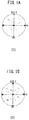
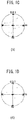
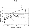
- Figs. 1A to 1D are normal pole point charts and Fig. 2 is a stress-strain diagram for EBSD evaluation of the representative samples. Note that (1), (2), (3), and (4) indicate the results for samples 1, 2, 5, and 6, respectively, in Figs. 1A to 1D and Fig. 2 .
- Figs. 1A to 1D are normal pole point charts of EBSD analysis results for copper plate samples 1, 2, 5, and 6. Each point denotes a measurement point in the normal pole point charts.
- the ⁇ 100> orientation is observed in the rolling direction, the normal direction, and the transverse direction for each sample, meaning that a strong recrystallization cube texture was formed in each sample.
- the percentage of the ⁇ 100> preferred orientation region calculated from measurement points when the ⁇ 100> orientation had a difference of not less than 15° with respect to both the foil rolling direction and the foil thickness direction was about 99%, which was substantially the same for each sample. Table 1 lists percentages of the ⁇ 100> preferred orientation region for the other samples.
- Fig. 2 depicts stress-strain curves obtained as a result of tensile test of samples of Figs. 1A to 1D .
- the textures of the four samples were substantially the same, the samples were significantly different from each other in terms of 0.2% proof stress, strength, and breaking elongation.
- the results for the other samples regarding 0.2% proof stress, strength, and breaking elongation are listed in Table 1.
- Sample 2 free from Cr had the smallest 0.2% proof stress and strength, the sample being annealed at 390°C for 1 hour, since high-purity copper was used, and recrystallization heat treatment was conducted at high temperatures, thereby causing the concentration of defects such as dislocations or holes to decrease.
- Sample 5 was a sample having a Cr concentration of 0.1% by mass which was obtained by conducting heat treatment at 390°C for 1 hour as in the case of sample 2, a slope of a line, 0.2% proof stress, and strength of sample 5 were greater than those of samples 1 and 2 in the low-strain area of the stress-strain curve, since Cr has the action of promoting precipitation.
- Sample 6 was a sample having a Cr concentration of 0.1% by mass, which was obtained by conducting heat treatment at 590°C for 1 hour as in the case of sample 5, strength was further improved, although the annealing temperature increased and the concentration of defects such as dislocations or holes decreased.
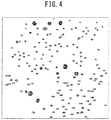
- Fig. 3 is a light field TEM image of sample 6, in which fine granular contrasts were observed.
- final anneal heat treatment caused recrystallization from the processed structure to the cube texture and aging precipitation of Cr to simultaneously proceed in a well-balanced manner.
- Fig. 4 is a binarized image of contrast between matrix and Cr precipitates in a visual field of the light field image (0.697 ⁇ m ⁇ 0.697 ⁇ m) of Fig. 3 , in which the precipitates are numbered.
- the number of precipitates and the area of each precipitate were determined to calculate density and mean particle size.
- the thickness of the TEM sample was 0.15 ⁇ m and the image was a transmission image, which means that the number of Cr precipitates present in the region with a size of 0.697 ⁇ 0.697 ⁇ 0.15 ⁇ m 3 was counted.
- the density of Cr precipitates in sample 6 was found to be 2287 precipitates/ ⁇ m 3 .
- the precipitate size was distributed from 4 nm to 36 nm and the mean diameter was 9.8 nm.
- the results of Table 1 suggest that the concentration at which formation of a cube texture with a percentage of the ⁇ 100> preferred orientation region of not less than 60.0% and promotion of Cr precipitation can be achieved is not less than 1.0% by mass.
- the concentration at which formation of a cube texture with a percentage of the ⁇ 100> preferred orientation region of not less than 70.0% and promotion of Cr precipitation could be achieved is less than 0.30% by mass.
- the concentration at which formation of a cube texture with a percentage of the ⁇ 100> preferred orientation region of not less than 80.0% and promotion of Cr precipitation could be achieved is less than 0.20% by mass.
- the purity of the copper plate designated as sample 13 was not less than 99%.
- 0.2% proof stress, strength, and breaking elongation were 115 MPa, 159 MPa, and 5.8%, which were relatively high.
- polishing was performed according to the sample preparation method in Example 1.
- the measurement system used in Example 1 was used to conduct texture analysis of a visual field of a measurement region of 80 ⁇ m ⁇ 160 ⁇ m at an accelerating voltage of 20 kV and a measurement step interval of 0.4 ⁇ m upon measurement.
- this sample was a polycrystal and having a grain size (area mean diameter) of about 2 ⁇ m without ⁇ 3 grain boundary.
- the percentage of the ⁇ 100> preferred orientation region was calculated in the manner described in Example 1 and it was 6.8%.
- N,N-dimethylacetamide was placed in a reaction container capable of nitrogen introduction, which was equipped with thermocouples and a stirrer.
- BAPP 2,2-bis [4-(4-aminophenoxy)phenyl]propane
- PMDA pyromellitic dianhydride
- N,N-dimethylacetamide was placed in a reaction container capable of nitrogen introduction, which was equipped with thermocouples and a stirrer.
- 2,2'-dimethyl-4,4'-diaminobiphenyl m-TB
- BPDA 3,3',4,4'-biphenyl-tetracarboxylic acid dianhydride
- PMDA pyromellitic dianhydride
- stirring was continued for 3 hours.
- a resin solution of polyamide acid b was obtained.
- the solution viscosity of the resin solution of polyamide acid b was 20,000 cps.
- the solution of polyamide acid a obtained in Synthetic Example 1 was applied to one surface of each of the copper plate samples 1 to 12 prepared in the above and dried (so that thermoplastic polyimide with a film thickness of 2 ⁇ m was formed after curing).
- the solution of polyamide acid b obtained in Synthetic Example 2 was applied to each coated surface and dried (so that low thermally expandable polyimide with a film thickness of 8 ⁇ m was formed after curing).
- the solution of polyamide acid a was further applied and dried (so that thermoplastic polyimide with a film thickness of 2 ⁇ m was formed after curing), followed by heating under conditions that applied heat at 280°C for an integration time of not less than 5 minutes. Accordingly, a polyimide layer having a three-layer structure was formed. Note that the heat treatment temperature was designated as polyimide formation temperature.
- a rectangular piece having a length of 250 mm in the rolling direction of the copper plate and a width of 40 mm in the direction perpendicular to the rolling direction was cut out so that a one-side copper-clad laminate test piece having a resin layer (polyimide) with a thickness of 12 ⁇ m and a copper plate layer with a thickness of 12 ⁇ m was obtained.
- modulus of elasticity in tension of the entire resin layer was 7.5 GPa.
- Lock seaming test was conducted using the flexible circuit board test pieces obtained above.
- the rolling (wiring) direction was designated as the folding direction.
- a crease was formed in the direction orthogonal to the rolling direction so that the wiring side became the interior side after folding (i.e., a bending portion was formed so that the direction of bending was orthogonal to the in-plane ⁇ 100> orientation of copper plate).
- Each flexible circuit board test piece was passed through a roller in parallel with the folding line while the roller was used to control a gap at the folding portion so that the gap became 0.3 mm.
- Table 2 indicated that when the oriented copper plate designated as sample 6 was used, the highest durability against lock seaming load was achieved, since the cube texture of sample 6 was developed and high levels of 0.2% proof stress, strength, and breaking elongation were achieved due to the effects of Cr precipitation.
- samples in which the cube texture was developed to bring the percentage of the ⁇ 100> preferred orientation region to about 99% were compared to each other. The comparison revealed that samples having greater effects of Cr precipitation had higher levels of lock seaming tolerability. Samples in which the cube texture was not developed had low levels of lock seaming tolerability even though Cr precipitation was observed.
- Scrap copper and Cr with a purity of not less than 99.5% by mass were used as raw materials. These were weighed in certain amounts, dissolved in a vacuum of not more than 10 -2 Pa using a high-purity graphite crucible, and casted in a high-purity graphite mold which was cooled via water-cooled copper hearth. The ingot had a size of 30 mm ⁇ 55 mm ⁇ 12 mm. This was hot rolled at 700°C so that a plate with a thickness of 1 mm was prepared.
- Hot rolling was conducted alternately in the 30-mm length direction and the 55-mm length direction by changing the hot rolling direction by 90° until the number of passages of the ingot reached 7.
- Middle annealing of a hot-rolled sheet with a thickness of 1 mm was conducted in nitrogen at 650°C for 2 hours together with Cr precipitation treatment.
- This copper plate material was cold rolled to result in a thickness of 0.4 mm.
- Slitting was conducted to adjust the width to 40 mm.
- cold rolling was conducted using a tension roller so that the final ND thickness was adjusted to 12 ⁇ m.
- the oriented copper plate having the final ND thickness which was obtained by rolling was analyzed for the Cr concentration by ICP spectrometry.
- Annealing was conducted by an operation of inserting copper foil from the outside of a heating zone into a hot soaking zone of a tube furnace that had been heated in advance to 400°C, taking copper foil outside of the heating zone after the elapse of 5 minutes, and cooling copper foil without oxidizing it.
- the conditions simulated the heat history of consecutive steps of forming polyimide on copper foil.
- Material structure and mechanical properties of produced copper foil were examined.
- the material structure was evaluated using EBSD employed for field-emission scanning electron microscopy (FE-SEM), and precipitation was evaluated by field-emission transmission electron microscopy (FE-TEM).
- FE-SEM field-emission scanning electron microscopy
- FE-TEM field-emission transmission electron microscopy
- tensile test was conducted for mechanical characteristics.
- Textures of the oriented copper plates were obtained by performing mechanical and chemical polishing on the rolling surface of each oriented copper plate using colloidal silica and conducting orientation analysis using an EBSD system.
- the systems used herein were FE-SEM (ZEISS Ultra 55), an EBSD system (TSL), and software (OIM Analysis 5.2).
- the measurement area was of 800 ⁇ m ⁇ 1600 ⁇ m.
- the accelerating voltage upon measurement was set to 20 kV and the measurement step interval was set to 4 ⁇ m (measurement was conducted so that measurement points formed a triangular lattice, the distance between measurement points was 4 ⁇ m, and the total measurement score was 92,631 points in the above region in this Example).
- the density of the cube texture of the present invention i.e., the ⁇ 100> preferred orientation region
- the density of the cube texture of the present invention may be expressed as a percentage of the measurement points at which the ⁇ 100> orientation has a difference of not more than 15° with respect to both the thickness direction of the copper plate and the rolling direction of the copper plate (i.e., the specific in-plane direction of the copper plate) with respect to the total measurement points.
- Two different visual fields were examined for each type of sample and the percentage was rounded to the nearest tenth to obtain the number of measurement points.
- crystal grains forming the ⁇ 100> preferred orientation region were large and some of them were greater than the above measured area.
- Each of the copper plates was thinned by electropolishing and the precipitate in each copper plate was assessed using FE-SEM (HF-2000) manufactured by Hitachi. The thickness of the measured area of each sample was 0.15 ⁇ m. Measurement was carried out at an accelerating voltage of 200 kV. The orientation of copper matrix was confirmed by electron diffraction. Composition analysis using electron diffraction and EDS analysis systems was employed for identification of the precipitates. The size and density of each precipitate were determined by processing the resulting image, determining a projected area for the contrast image of each obtained precipitate, and calculating the equivalent circle diameter.
- a specimen having a length of 150 mm and a width of 10 mm was cut out from each copper plate to conduct a tensile test at a gauge distance of 100 mm and a tensile speed of 10 mm/minutes in parallel to the rolling direction.
- a stress-strain diagram was created based on the results obtained from the tensile test for evaluation in terms of 0.2% proof stress value, strength, and breaking elongation. Stress is a value obtained by dividing a load on the load cell by the cross-sectional area of a copper plate before tensile test. Strain corresponds to displacement of a crosshead of a tensile tester with respect to the gauge distance, which is expressed as a percentage.
- the maximum value of the amount of Cr added for bringing the ⁇ 100> preferred orientation region to not less than 60.0% was 0.38% by mass and maximum value of the amount of Cr added for bringing the ⁇ 100> preferred orientation region to more than 70.0% was less than 0.30% by mass.
- the range of the amount of Cr added is decreased, at which both advanced cube texture formation and Cr precipitation promotion can be achieved, since the heat history in the final annealing step was small.
- the percentage of the ⁇ 100> preferred orientation region of copper foil corresponding to sample 14 free from Cr was as small as about 70%, although the Cr content was small, since as the Cr content was small, crystal grains were coarsened as a result of middle annealing at 650°C for 2 hours, and then, a cube orientation was not developed during final annealing as uniform processing strain was not introduced during cold working.
- Sample 17 having the ⁇ 100> preferred orientation region comparable to that of sample 14 and sample 18 having a low percentage of ⁇ 100> preferred orientation region had a fewer number of small cracks as a result of promotion due to Cr precipitation.
- the Cr concentration may be not more than 0.38% by mass, desirably less than 0.30% by mass, and more desirably less than 0.20% by mass.
- the optimal value would vary depending on the heat history of the step of laminating copper foil and polyimide. It is desirable to maximize the Cr content in a range in which crystal grains having the ⁇ 100> preferred orientation can be developed.
- the percentage of the ⁇ 100> preferred orientation region of sample 16b was 70.9% and the strength thereof was 148 Pa. The strength was smaller than that of sample 16, since the amount of Cr precipitates decreased as precipitation heat treatment was not conducted, resulting in a small action of promoting precipitation.
- the area percentage of the ⁇ 100> preferred orientation region of sample 16b was smaller than that of sample 16, since a large amount of Cr solid solution in copper caused the recrystallization temperature to increase to a level greater than that of sample 16, thereby preventing sufficient progress in recrystallization under the final annealing conditions of the present invention.
- Oxygen-free copper having a purity of not less than 99.96%, Cr, Zr, Zn, and phosphorus deoxidized copper containing 2.8% by weight of P were used as raw materials. These were weighed in certain amounts, dissolved in a vacuum of not more than 10 -2 Pa using a high-purity graphite crucible, and casted in a high-purity graphite mold cooled via water-cooled copper hearth. The ingot had a size of ⁇ 20 mm ⁇ 100 mm. The surface thereof was reduced by swaging to result in ⁇ 6 mm.
- the ingot was stretched via cross rolling such that a tape-shaped plate material having a width of 18 mm and a thickness of 1.5 mm was obtained.
- the thickness was adjusted to 0.2 mm via cold rolling, following which slitting was conducted in the length direction such that a tape-shaped plate material having a width of 1.3 mm and a thickness of 0.2 mm was obtained.
- This material was wound around a stainless-steel bobbin, followed by precipitation, recrystallization, and annealing in vacuum at 650°C for 2 hours. Thus, a final sample was obtained.
- the material textures were evaluated by EBSD combined with field-emission scanning electron microscopy (FE-SEM) and precipitates were evaluated by field-emission transmission electron microscopy (FE-TEM).
- Textures of the oriented copper plates were obtained by performing mechanical and chemical polishing on the rolling surface of each oriented copper plate using colloidal silica and conducting orientation analysis using an EBSD system.
- the systems used herein were FE-SEM (ZEISS Ultra 55), an EBSD system (TSL), and software (OIM Analysis 5.2).
- the measurement area was of 800 ⁇ m ⁇ 1600 ⁇ m.
- the accelerating voltage upon measurement was set to 20 kV and the measurement step interval was set to 4 ⁇ m (measurement was conducted so that measurement points formed a triangular lattice, the distance between measurement points was 4 ⁇ m, and the total measurement score was 92,631 points in the above region in this Example).
- the density of the cube texture of the present invention i.e., the ⁇ 100> preferred orientation region
- the density of the cube texture of the present invention may be expressed as a percentage of the measurement points at which the ⁇ 100> orientation has a difference of not more than 15° with respect to both the thickness direction of the copper plate and the rolling direction of the copper plate (i.e., the specific in-plane direction of the copper plate) with respect to the total measurement points.
- Two different visual fields were examined for each type of sample and the percentage was rounded to the nearest tenth to obtain the number of measurement points.
- NSC-150-SM full automatic wiring system
- This wiring system is capable of feeding a tape-shaped plate material from a bobbin at a certain tension, cutting the tape-shaped plate material to a length of 320 m, and embossing the center portion of a cut piece of the tape-shaped plate material using a step mold so as to form two 90° folds, which are a mountain fold and a valley fold, in a direction vertical to the length direction and the normal direction.
- the plate material to have a gap of about 150 ⁇ m in the thickness direction at the center portion of the length direction, and therefore bond an acceptance surface of a solar cell may be bonded a back face of an adjacent solar cell, by narrowing the distance between the cells.
- the percentage of the ⁇ 100> preferred orientation region for samples containing Zr was not less than 80.0%, even though the concentration of Zr was 0.1% by mass. On the other hand, no sample having the ⁇ 100> preferred orientation region at not less than 60.0% was obtained among sample 22 containing P at 0.01% by mass, sample 24 containing Zn at 0.1% by mass.
- an oriented copper plate may be provided, which has high levels of yield strength, mechanical strength, and breaking elongation greater than those of conventional materials having similar levels of cube texture concentration by material structure characteristics of both advanced cube texture and Cr precipitation, and excellent folding flexibility, which can be used a wide range of applications such as solar cell wiring materials and various circuit board materials having an insulating layer composed of plastic or ceramic.
- a flexible circuit board for devices, in which a bending portion is formed, the bending portion needing to be frequently folded via repetition of actions such as rotary slide bending, folding bending, hinge bending, and lateral slide bending and having a very small radius of curvature. Therefore, such a flexible circuit board can be suitably used for a variety of electronics such as thin mobile phones which needs durability, thin displays, hard disks, printers, and DVD devices.
Landscapes
- Engineering & Computer Science (AREA)
- Chemical & Material Sciences (AREA)
- Microelectronics & Electronic Packaging (AREA)
- Mechanical Engineering (AREA)
- Organic Chemistry (AREA)
- Metallurgy (AREA)
- Materials Engineering (AREA)
- Manufacturing & Machinery (AREA)
- Physics & Mathematics (AREA)
- Crystallography & Structural Chemistry (AREA)
- Thermal Sciences (AREA)
- Parts Printed On Printed Circuit Boards (AREA)
- Non-Insulated Conductors (AREA)
- Conductive Materials (AREA)
- Laminated Bodies (AREA)
Claims (7)
- Ein orientiertes Kupferblech, welches 0,03 Massen-% bis 1,0 Massen-% Cr enthält, welches gegebenenfalls ferner eines oder zwei oder mehrere enthält von: Mn: nicht mehr als 0,4 Massen-%; Al: nicht mehr als 0,4 Massen-%; Ti: nicht mehr als 0,2 Massen-%; Zr: nicht mehr als 0,2 Massen-%; und Seltenerdelemente: nicht mehr als 0,4 Massen-%, welches gegebenenfalls ferner eines oder zwei enthält von: P: weniger als 0,01 Massen-%; und Zn: weniger als 0,1 Massen-%, und/oder welches gegebenenfalls ferner, in einer Gesamtkonzentration von weniger als 0,03 Massen-%, eines oder zwei oder mehrere ausgewählt aus der Gruppe bestehend aus: Ag, Sn, Pd, Ni, Fe, B, Si, Ca, V, Co, Ga, Ge, Sr, Nb, Mo, Rh, Ba, W und Pt enthält, wobei der Rest davon aus Kupfer und unvermeidbaren Verunreinigungen besteht, wobei das Kupferblech eine <100> Hauptorientierung aufweist, so dass der Flächenanteil eines bevorzugten <100> Orientierungsbereichs nicht weniger als 60,0% beträgt, wobei der Bereich eine Bedingung erfüllt, welche es zulässt, dass sowohl eine Dickenrichtung des Kupferblechs als auch eine spezifische Richtung in der Ebene des Kupferblechs eine Orientierungsdifferenz von nicht mehr als 15°, bezogen auf eine <100> Kupferkristallachse, aufweist, und wobei Cr-Ausfällungen mit äquivalenten Kreisdurchmessern von 4 nm bis 52 nm als 300 Ausfällungen/µm3 bis 12000 Ausfällungen/µm3 vorliegen.
- Ein kupferkaschiertes Laminat, welches eine isolierende Schicht aufweist, welche auf einer Oberfläche des orientierten Kupferblechs gemäß Anspruch 1 gebildet ist.
- Das kupferkaschierte Laminat gemäß Anspruch 2, wobei das orientierte Kupferblech eine Dicke von 5 µm bis 18 µm aufweist und die isolierende Schicht aus einem Harz besteht und eine Dicke von 5 µm bis 75 µm aufweist.
- Das kupferkaschierte Laminat gemäß Anspruch 3, wobei das Harz aus Polyimid besteht.
- Eine flexible Leiterplatte, welches eine bestimmte auf dem orientieren Kupferblech des kupferkaschierten Laminats gemäß einem der Ansprüche 2 bis 4 gebildete Verkabelung aufweist, welche ferner einen Biegebereich an mindestens einer Stelle der Verkabelung in einer Richtung orthogonal zu einer spezifischen Richtung in der Ebene des Kupferblechs aufweist.
- Die flexible Leiterplatte gemäß Anspruch 5, wobei der Biegebereicht ein Biegebereich ist, welcher eine oder zwei oder mehrere Wiederholungsaktionen ausführt, ausgewählt aus der Gruppe bestehend aus Falzbiegen, Drehschiebebiegen, Abkantbiegen, Scharnierbiegen und seitlichem Schiebebiegen.
- Eine elektronische Vorrichtung, welche mit der flexiblen Leiterplatte gemäß Anspruch 5 oder 6 ausgestattet ist.
Applications Claiming Priority (2)
| Application Number | Priority Date | Filing Date | Title |
|---|---|---|---|
| JP2014252321 | 2014-12-12 | ||
| PCT/JP2015/084822 WO2016093349A1 (ja) | 2014-12-12 | 2015-12-11 | 配向銅板、銅張積層板、可撓性回路基板、及び電子機器 |
Publications (3)
| Publication Number | Publication Date |
|---|---|
| EP3231880A1 EP3231880A1 (de) | 2017-10-18 |
| EP3231880A4 EP3231880A4 (de) | 2018-07-11 |
| EP3231880B1 true EP3231880B1 (de) | 2020-10-21 |
Family
ID=56107526
Family Applications (1)
| Application Number | Title | Priority Date | Filing Date |
|---|---|---|---|
| EP15866605.7A Active EP3231880B1 (de) | 2014-12-12 | 2015-12-11 | Orientiertes kupferblech, kupferkaschiertes laminat, flexible leiterplatte und elektronische vorrichtung |
Country Status (7)
| Country | Link |
|---|---|
| US (1) | US9883588B2 (de) |
| EP (1) | EP3231880B1 (de) |
| JP (1) | JP6358340B2 (de) |
| KR (1) | KR101915422B1 (de) |
| CN (1) | CN107109534B (de) |
| TW (1) | TWI582248B (de) |
| WO (1) | WO2016093349A1 (de) |
Families Citing this family (5)
| Publication number | Priority date | Publication date | Assignee | Title |
|---|---|---|---|---|
| PH12017000015A1 (en) * | 2016-01-15 | 2018-08-06 | Jx Nippon Mining & Metals Corp | Copper foil, copper-clad laminate board, method for producing printed wiring board, method for poducing electronic apparatus, method for producing transmission channel, and method for producing antenna |
| KR20190133736A (ko) * | 2017-03-30 | 2019-12-03 | 제이엑스금속주식회사 | 압연 구리박 |
| US12463171B2 (en) * | 2019-12-02 | 2025-11-04 | Nippon Micrometal Corporation | Copper bonding wire for semiconductor devices and semiconductor device |
| JP6900137B1 (ja) * | 2020-01-14 | 2021-07-07 | 古河電気工業株式会社 | 銅合金板材およびその製造方法、ならびに電気・電子部品用部材 |
| TWI814182B (zh) * | 2021-12-21 | 2023-09-01 | 鉑識科技股份有限公司 | 複合銅層及其製備方法 |
Family Cites Families (16)
| Publication number | Priority date | Publication date | Assignee | Title |
|---|---|---|---|---|
| JP3009383B2 (ja) | 1998-03-31 | 2000-02-14 | 日鉱金属株式会社 | 圧延銅箔およびその製造方法 |
| WO2003064722A1 (en) * | 2002-01-30 | 2003-08-07 | Nikko Materials Company, Limited | Copper alloy sputtering target and method for manufacturing the target |
| EP2045344B1 (de) * | 2006-07-21 | 2012-05-23 | Kabushiki Kaisha Kobe Seiko Sho | Verfahren zum herstellen von kupferlegierungsblechen für elektrisches/elektronisches teil |
| JP4763068B2 (ja) | 2008-06-30 | 2011-08-31 | 新日鐵化学株式会社 | 可撓性回路基板及びその製造方法並びに可撓性回路基板の屈曲部構造 |
| KR101580822B1 (ko) * | 2008-06-30 | 2015-12-30 | 신닛테츠 수미킨 가가쿠 가부시키가이샤 | 가요성 회로기판 및 그 제조방법 그리고 가요성 회로기판의 굴곡부 구조 |
| JP5446188B2 (ja) | 2008-09-17 | 2014-03-19 | 新日鐵住金株式会社 | 半導体線実装用のインターコネクター及び太陽電池用インターコネクター |
| JP5462069B2 (ja) * | 2009-07-27 | 2014-04-02 | 株式会社神戸製鋼所 | 落重特性および母材靭性に優れた高強度厚鋼板 |
| WO2011115305A1 (ja) | 2010-03-17 | 2011-09-22 | 新日本製鐵株式会社 | 金属テープ材料、及び太陽電池集電用インターコネクター |
| CN102985572B (zh) * | 2010-07-07 | 2014-09-03 | 三菱伸铜株式会社 | 深冲压加工性优异的Cu-Ni-Si系铜合金板及其制造方法 |
| JP5170916B2 (ja) * | 2010-08-27 | 2013-03-27 | 古河電気工業株式会社 | 銅合金板材及びその製造方法 |
| KR101886824B1 (ko) * | 2011-03-31 | 2018-08-08 | 신닛테츠 수미킨 가가쿠 가부시키가이샤 | 동박, 동장 적층판, 가요성 회로기판 및 동장 적층판의 제조방법 |
| KR101953412B1 (ko) * | 2011-08-05 | 2019-02-28 | 후루카와 덴키 고교 가부시키가이샤 | 이차전지 집전체용 압연 동박 및 그 제조방법 |
| WO2013031841A1 (ja) * | 2011-08-29 | 2013-03-07 | 古河電気工業株式会社 | 銅合金材料およびその製造方法 |
| EP2765215B1 (de) * | 2011-11-11 | 2017-05-03 | Furukawa Electric Co., Ltd. | Gewalzte kupferfolie |
| JP2013194246A (ja) * | 2012-03-15 | 2013-09-30 | Mitsubishi Shindoh Co Ltd | 残留応力の少ないリードフレーム用Cu−Cr−Sn系銅合金板 |
| WO2014115307A1 (ja) * | 2013-01-25 | 2014-07-31 | 三菱伸銅株式会社 | 端子・コネクタ材用銅合金板及び端子・コネクタ材用銅合金板の製造方法 |
-
2015
- 2015-12-11 EP EP15866605.7A patent/EP3231880B1/de active Active
- 2015-12-11 KR KR1020177015273A patent/KR101915422B1/ko not_active Expired - Fee Related
- 2015-12-11 TW TW104141761A patent/TWI582248B/zh not_active IP Right Cessation
- 2015-12-11 US US15/533,195 patent/US9883588B2/en active Active
- 2015-12-11 WO PCT/JP2015/084822 patent/WO2016093349A1/ja not_active Ceased
- 2015-12-11 JP JP2016563751A patent/JP6358340B2/ja active Active
- 2015-12-11 CN CN201580067345.1A patent/CN107109534B/zh active Active
Non-Patent Citations (1)
| Title |
|---|
| None * |
Also Published As
| Publication number | Publication date |
|---|---|
| US9883588B2 (en) | 2018-01-30 |
| US20170332489A1 (en) | 2017-11-16 |
| CN107109534A (zh) | 2017-08-29 |
| TW201625804A (zh) | 2016-07-16 |
| EP3231880A1 (de) | 2017-10-18 |
| WO2016093349A1 (ja) | 2016-06-16 |
| TWI582248B (zh) | 2017-05-11 |
| KR101915422B1 (ko) | 2018-11-05 |
| JP6358340B2 (ja) | 2018-07-18 |
| EP3231880A4 (de) | 2018-07-11 |
| CN107109534B (zh) | 2018-11-09 |
| JPWO2016093349A1 (ja) | 2017-11-02 |
| KR20170083076A (ko) | 2017-07-17 |
Similar Documents
| Publication | Publication Date | Title |
|---|---|---|
| CN103361509B (zh) | 轧制铜箔、覆铜层叠板、柔性印刷布线板及其制造方法 | |
| EP3231880B1 (de) | Orientiertes kupferblech, kupferkaschiertes laminat, flexible leiterplatte und elektronische vorrichtung | |
| JP4716520B2 (ja) | 圧延銅箔 | |
| TWI768097B (zh) | 高強度與高導電性的銅合金板材及其製造方法 | |
| US7789977B2 (en) | Rolled copper foil and manufacturing method thereof | |
| JPWO2009148101A1 (ja) | 銅合金板材およびその製造方法 | |
| CN102892908A (zh) | 电子器件用铜合金、电子器件用铜合金的制造方法及电子器件用铜合金轧材 | |
| CN103415635B (zh) | 铜箔、覆铜层叠板、挠性电路基板及覆铜层叠板的制造方法 | |
| CN102985572A (zh) | 深冲压加工性优异的Cu-Ni-Si系铜合金板及其制造方法 | |
| KR20140145062A (ko) | 우수한 내피로특성을 가지는 Cu―Mg―P계 구리합금판 및 그 제조방법 | |
| KR102098479B1 (ko) | 플렉시블 프린트 기판용 구리박, 그것을 사용한 구리 피복 적층체, 플렉시블 프린트 기판 및 전자 기기 | |
| JP6294257B2 (ja) | フレキシブルプリント基板用銅合金箔、それを用いた銅張積層体、フレキシブルプリント基板、及び電子機器 | |
| JP6126799B2 (ja) | 銅箔、銅張積層板、可撓性回路基板、及び銅張積層板の製造方法 | |
| JP5865759B2 (ja) | 銅箔、銅張積層板、可撓性回路基板、及び銅張積層板の製造方法 | |
| KR20150023874A (ko) | 구리 합금 및 그의 제조 방법 | |
| KR20190015109A (ko) | 플렉시블 프린트 기판용 구리박, 그것을 사용한 구리 피복 적층체, 플렉시블 프린트 기판, 및 전자 기기 | |
| JP2010280191A (ja) | 熱処理用銅箔、熱処理用銅箔の製造方法およびフレキシブルプリント配線板 | |
| JP2001144391A (ja) | プリント回路基板用圧延銅箔およびその製造方法 | |
| TWI639163B (zh) | Cu-Co-Ni-Si alloy for electronic parts, and electronic parts | |
| JP2007126687A (ja) | 銅合金箔 | |
| CN119256110A (zh) | 压延铜箔、覆铜层叠板、覆铜层叠板的制造方法、柔性印刷线路板的制造方法以及电子部件的制造方法 |
Legal Events
| Date | Code | Title | Description |
|---|---|---|---|
| STAA | Information on the status of an ep patent application or granted ep patent |
Free format text: STATUS: THE INTERNATIONAL PUBLICATION HAS BEEN MADE |
|
| PUAI | Public reference made under article 153(3) epc to a published international application that has entered the european phase |
Free format text: ORIGINAL CODE: 0009012 |
|
| STAA | Information on the status of an ep patent application or granted ep patent |
Free format text: STATUS: REQUEST FOR EXAMINATION WAS MADE |
|
| 17P | Request for examination filed |
Effective date: 20170619 |
|
| AK | Designated contracting states |
Kind code of ref document: A1 Designated state(s): AL AT BE BG CH CY CZ DE DK EE ES FI FR GB GR HR HU IE IS IT LI LT LU LV MC MK MT NL NO PL PT RO RS SE SI SK SM TR |
|
| AX | Request for extension of the european patent |
Extension state: BA ME |
|
| DAV | Request for validation of the european patent (deleted) | ||
| DAX | Request for extension of the european patent (deleted) | ||
| A4 | Supplementary search report drawn up and despatched |
Effective date: 20180613 |
|
| RIC1 | Information provided on ipc code assigned before grant |
Ipc: C22F 1/08 20060101ALI20180607BHEP Ipc: C22C 9/00 20060101AFI20180607BHEP Ipc: H01B 5/02 20060101ALI20180607BHEP Ipc: H05K 1/05 20060101ALI20180607BHEP Ipc: C22F 1/00 20060101ALI20180607BHEP Ipc: H01B 1/02 20060101ALI20180607BHEP |
|
| RAP1 | Party data changed (applicant data changed or rights of an application transferred) |
Owner name: NIPPON STEEL CORPORATION |
|
| STAA | Information on the status of an ep patent application or granted ep patent |
Free format text: STATUS: EXAMINATION IS IN PROGRESS |
|
| 17Q | First examination report despatched |
Effective date: 20190909 |
|
| GRAP | Despatch of communication of intention to grant a patent |
Free format text: ORIGINAL CODE: EPIDOSNIGR1 |
|
| STAA | Information on the status of an ep patent application or granted ep patent |
Free format text: STATUS: GRANT OF PATENT IS INTENDED |
|
| INTG | Intention to grant announced |
Effective date: 20200504 |
|
| GRAS | Grant fee paid |
Free format text: ORIGINAL CODE: EPIDOSNIGR3 |
|
| GRAA | (expected) grant |
Free format text: ORIGINAL CODE: 0009210 |
|
| STAA | Information on the status of an ep patent application or granted ep patent |
Free format text: STATUS: THE PATENT HAS BEEN GRANTED |
|
| AK | Designated contracting states |
Kind code of ref document: B1 Designated state(s): AL AT BE BG CH CY CZ DE DK EE ES FI FR GB GR HR HU IE IS IT LI LT LU LV MC MK MT NL NO PL PT RO RS SE SI SK SM TR |
|
| REG | Reference to a national code |
Ref country code: GB Ref legal event code: FG4D |
|
| REG | Reference to a national code |
Ref country code: CH Ref legal event code: EP |
|
| REG | Reference to a national code |
Ref country code: IE Ref legal event code: FG4D |
|
| REG | Reference to a national code |
Ref country code: DE Ref legal event code: R096 Ref document number: 602015060940 Country of ref document: DE |
|
| REG | Reference to a national code |
Ref country code: AT Ref legal event code: REF Ref document number: 1325946 Country of ref document: AT Kind code of ref document: T Effective date: 20201115 |
|
| REG | Reference to a national code |
Ref country code: AT Ref legal event code: MK05 Ref document number: 1325946 Country of ref document: AT Kind code of ref document: T Effective date: 20201021 |
|
| REG | Reference to a national code |
Ref country code: NL Ref legal event code: MP Effective date: 20201021 |
|
| PG25 | Lapsed in a contracting state [announced via postgrant information from national office to epo] |
Ref country code: PT Free format text: LAPSE BECAUSE OF FAILURE TO SUBMIT A TRANSLATION OF THE DESCRIPTION OR TO PAY THE FEE WITHIN THE PRESCRIBED TIME-LIMIT Effective date: 20210222 Ref country code: RS Free format text: LAPSE BECAUSE OF FAILURE TO SUBMIT A TRANSLATION OF THE DESCRIPTION OR TO PAY THE FEE WITHIN THE PRESCRIBED TIME-LIMIT Effective date: 20201021 Ref country code: FI Free format text: LAPSE BECAUSE OF FAILURE TO SUBMIT A TRANSLATION OF THE DESCRIPTION OR TO PAY THE FEE WITHIN THE PRESCRIBED TIME-LIMIT Effective date: 20201021 Ref country code: NL Free format text: LAPSE BECAUSE OF FAILURE TO SUBMIT A TRANSLATION OF THE DESCRIPTION OR TO PAY THE FEE WITHIN THE PRESCRIBED TIME-LIMIT Effective date: 20201021 Ref country code: NO Free format text: LAPSE BECAUSE OF FAILURE TO SUBMIT A TRANSLATION OF THE DESCRIPTION OR TO PAY THE FEE WITHIN THE PRESCRIBED TIME-LIMIT Effective date: 20210121 Ref country code: GR Free format text: LAPSE BECAUSE OF FAILURE TO SUBMIT A TRANSLATION OF THE DESCRIPTION OR TO PAY THE FEE WITHIN THE PRESCRIBED TIME-LIMIT Effective date: 20210122 |
|
| REG | Reference to a national code |
Ref country code: LT Ref legal event code: MG4D |
|
| PG25 | Lapsed in a contracting state [announced via postgrant information from national office to epo] |
Ref country code: AT Free format text: LAPSE BECAUSE OF FAILURE TO SUBMIT A TRANSLATION OF THE DESCRIPTION OR TO PAY THE FEE WITHIN THE PRESCRIBED TIME-LIMIT Effective date: 20201021 Ref country code: ES Free format text: LAPSE BECAUSE OF FAILURE TO SUBMIT A TRANSLATION OF THE DESCRIPTION OR TO PAY THE FEE WITHIN THE PRESCRIBED TIME-LIMIT Effective date: 20201021 Ref country code: BG Free format text: LAPSE BECAUSE OF FAILURE TO SUBMIT A TRANSLATION OF THE DESCRIPTION OR TO PAY THE FEE WITHIN THE PRESCRIBED TIME-LIMIT Effective date: 20210121 Ref country code: PL Free format text: LAPSE BECAUSE OF FAILURE TO SUBMIT A TRANSLATION OF THE DESCRIPTION OR TO PAY THE FEE WITHIN THE PRESCRIBED TIME-LIMIT Effective date: 20201021 Ref country code: SE Free format text: LAPSE BECAUSE OF FAILURE TO SUBMIT A TRANSLATION OF THE DESCRIPTION OR TO PAY THE FEE WITHIN THE PRESCRIBED TIME-LIMIT Effective date: 20201021 Ref country code: LV Free format text: LAPSE BECAUSE OF FAILURE TO SUBMIT A TRANSLATION OF THE DESCRIPTION OR TO PAY THE FEE WITHIN THE PRESCRIBED TIME-LIMIT Effective date: 20201021 Ref country code: IS Free format text: LAPSE BECAUSE OF FAILURE TO SUBMIT A TRANSLATION OF THE DESCRIPTION OR TO PAY THE FEE WITHIN THE PRESCRIBED TIME-LIMIT Effective date: 20210221 |
|
| PG25 | Lapsed in a contracting state [announced via postgrant information from national office to epo] |
Ref country code: HR Free format text: LAPSE BECAUSE OF FAILURE TO SUBMIT A TRANSLATION OF THE DESCRIPTION OR TO PAY THE FEE WITHIN THE PRESCRIBED TIME-LIMIT Effective date: 20201021 |
|
| REG | Reference to a national code |
Ref country code: DE Ref legal event code: R097 Ref document number: 602015060940 Country of ref document: DE |
|
| PG25 | Lapsed in a contracting state [announced via postgrant information from national office to epo] |
Ref country code: RO Free format text: LAPSE BECAUSE OF FAILURE TO SUBMIT A TRANSLATION OF THE DESCRIPTION OR TO PAY THE FEE WITHIN THE PRESCRIBED TIME-LIMIT Effective date: 20201021 Ref country code: SK Free format text: LAPSE BECAUSE OF FAILURE TO SUBMIT A TRANSLATION OF THE DESCRIPTION OR TO PAY THE FEE WITHIN THE PRESCRIBED TIME-LIMIT Effective date: 20201021 Ref country code: SM Free format text: LAPSE BECAUSE OF FAILURE TO SUBMIT A TRANSLATION OF THE DESCRIPTION OR TO PAY THE FEE WITHIN THE PRESCRIBED TIME-LIMIT Effective date: 20201021 Ref country code: LT Free format text: LAPSE BECAUSE OF FAILURE TO SUBMIT A TRANSLATION OF THE DESCRIPTION OR TO PAY THE FEE WITHIN THE PRESCRIBED TIME-LIMIT Effective date: 20201021 Ref country code: EE Free format text: LAPSE BECAUSE OF FAILURE TO SUBMIT A TRANSLATION OF THE DESCRIPTION OR TO PAY THE FEE WITHIN THE PRESCRIBED TIME-LIMIT Effective date: 20201021 Ref country code: CZ Free format text: LAPSE BECAUSE OF FAILURE TO SUBMIT A TRANSLATION OF THE DESCRIPTION OR TO PAY THE FEE WITHIN THE PRESCRIBED TIME-LIMIT Effective date: 20201021 |
|
| REG | Reference to a national code |
Ref country code: CH Ref legal event code: PL |
|
| PLBE | No opposition filed within time limit |
Free format text: ORIGINAL CODE: 0009261 |
|
| STAA | Information on the status of an ep patent application or granted ep patent |
Free format text: STATUS: NO OPPOSITION FILED WITHIN TIME LIMIT |
|
| PG25 | Lapsed in a contracting state [announced via postgrant information from national office to epo] |
Ref country code: DK Free format text: LAPSE BECAUSE OF FAILURE TO SUBMIT A TRANSLATION OF THE DESCRIPTION OR TO PAY THE FEE WITHIN THE PRESCRIBED TIME-LIMIT Effective date: 20201021 Ref country code: MC Free format text: LAPSE BECAUSE OF FAILURE TO SUBMIT A TRANSLATION OF THE DESCRIPTION OR TO PAY THE FEE WITHIN THE PRESCRIBED TIME-LIMIT Effective date: 20201021 |
|
| REG | Reference to a national code |
Ref country code: BE Ref legal event code: MM Effective date: 20201231 |
|
| 26N | No opposition filed |
Effective date: 20210722 |
|
| GBPC | Gb: european patent ceased through non-payment of renewal fee |
Effective date: 20210121 |
|
| PG25 | Lapsed in a contracting state [announced via postgrant information from national office to epo] |
Ref country code: FR Free format text: LAPSE BECAUSE OF NON-PAYMENT OF DUE FEES Effective date: 20201221 Ref country code: LU Free format text: LAPSE BECAUSE OF NON-PAYMENT OF DUE FEES Effective date: 20201211 Ref country code: AL Free format text: LAPSE BECAUSE OF FAILURE TO SUBMIT A TRANSLATION OF THE DESCRIPTION OR TO PAY THE FEE WITHIN THE PRESCRIBED TIME-LIMIT Effective date: 20201021 Ref country code: IE Free format text: LAPSE BECAUSE OF NON-PAYMENT OF DUE FEES Effective date: 20201211 Ref country code: IT Free format text: LAPSE BECAUSE OF FAILURE TO SUBMIT A TRANSLATION OF THE DESCRIPTION OR TO PAY THE FEE WITHIN THE PRESCRIBED TIME-LIMIT Effective date: 20201021 |
|
| PG25 | Lapsed in a contracting state [announced via postgrant information from national office to epo] |
Ref country code: SI Free format text: LAPSE BECAUSE OF FAILURE TO SUBMIT A TRANSLATION OF THE DESCRIPTION OR TO PAY THE FEE WITHIN THE PRESCRIBED TIME-LIMIT Effective date: 20201021 Ref country code: CH Free format text: LAPSE BECAUSE OF NON-PAYMENT OF DUE FEES Effective date: 20201231 Ref country code: GB Free format text: LAPSE BECAUSE OF NON-PAYMENT OF DUE FEES Effective date: 20210121 Ref country code: LI Free format text: LAPSE BECAUSE OF NON-PAYMENT OF DUE FEES Effective date: 20201231 |
|
| PG25 | Lapsed in a contracting state [announced via postgrant information from national office to epo] |
Ref country code: IS Free format text: LAPSE BECAUSE OF FAILURE TO SUBMIT A TRANSLATION OF THE DESCRIPTION OR TO PAY THE FEE WITHIN THE PRESCRIBED TIME-LIMIT Effective date: 20210221 Ref country code: TR Free format text: LAPSE BECAUSE OF FAILURE TO SUBMIT A TRANSLATION OF THE DESCRIPTION OR TO PAY THE FEE WITHIN THE PRESCRIBED TIME-LIMIT Effective date: 20201021 Ref country code: MT Free format text: LAPSE BECAUSE OF FAILURE TO SUBMIT A TRANSLATION OF THE DESCRIPTION OR TO PAY THE FEE WITHIN THE PRESCRIBED TIME-LIMIT Effective date: 20201021 Ref country code: CY Free format text: LAPSE BECAUSE OF FAILURE TO SUBMIT A TRANSLATION OF THE DESCRIPTION OR TO PAY THE FEE WITHIN THE PRESCRIBED TIME-LIMIT Effective date: 20201021 |
|
| PG25 | Lapsed in a contracting state [announced via postgrant information from national office to epo] |
Ref country code: MK Free format text: LAPSE BECAUSE OF FAILURE TO SUBMIT A TRANSLATION OF THE DESCRIPTION OR TO PAY THE FEE WITHIN THE PRESCRIBED TIME-LIMIT Effective date: 20201021 |
|
| PG25 | Lapsed in a contracting state [announced via postgrant information from national office to epo] |
Ref country code: BE Free format text: LAPSE BECAUSE OF NON-PAYMENT OF DUE FEES Effective date: 20201231 |
|
| PGFP | Annual fee paid to national office [announced via postgrant information from national office to epo] |
Ref country code: DE Payment date: 20251028 Year of fee payment: 11 |