EP3221885B1 - High resistivity semiconductor-on-insulator wafer and a method of manufacturing - Google Patents
High resistivity semiconductor-on-insulator wafer and a method of manufacturing Download PDFInfo
- Publication number
- EP3221885B1 EP3221885B1 EP15801615.4A EP15801615A EP3221885B1 EP 3221885 B1 EP3221885 B1 EP 3221885B1 EP 15801615 A EP15801615 A EP 15801615A EP 3221885 B1 EP3221885 B1 EP 3221885B1
- Authority
- EP
- European Patent Office
- Prior art keywords
- single crystal
- crystal semiconductor
- layer
- handle substrate
- silicon
- Prior art date
- Legal status (The legal status is an assumption and is not a legal conclusion. Google has not performed a legal analysis and makes no representation as to the accuracy of the status listed.)
- Active
Links
Images
Classifications
-
- H—ELECTRICITY
- H10—SEMICONDUCTOR DEVICES; ELECTRIC SOLID-STATE DEVICES NOT OTHERWISE PROVIDED FOR
- H10P—GENERIC PROCESSES OR APPARATUS FOR THE MANUFACTURE OR TREATMENT OF DEVICES COVERED BY CLASS H10
- H10P90/00—Preparation of wafers not covered by a single main group of this subclass, e.g. wafer reinforcement
- H10P90/19—Preparing inhomogeneous wafers
- H10P90/1904—Preparing vertically inhomogeneous wafers
- H10P90/1906—Preparing SOI wafers
- H10P90/1914—Preparing SOI wafers using bonding
- H10P90/1916—Preparing SOI wafers using bonding with separation or delamination along an ion implanted layer, e.g. Smart-cut
-
- H—ELECTRICITY
- H10—SEMICONDUCTOR DEVICES; ELECTRIC SOLID-STATE DEVICES NOT OTHERWISE PROVIDED FOR
- H10P—GENERIC PROCESSES OR APPARATUS FOR THE MANUFACTURE OR TREATMENT OF DEVICES COVERED BY CLASS H10
- H10P90/00—Preparation of wafers not covered by a single main group of this subclass, e.g. wafer reinforcement
-
- H—ELECTRICITY
- H10—SEMICONDUCTOR DEVICES; ELECTRIC SOLID-STATE DEVICES NOT OTHERWISE PROVIDED FOR
- H10W—GENERIC PACKAGES, INTERCONNECTIONS, CONNECTORS OR OTHER CONSTRUCTIONAL DETAILS OF DEVICES COVERED BY CLASS H10
- H10W10/00—Isolation regions in semiconductor bodies between components of integrated devices
- H10W10/10—Isolation regions comprising dielectric materials
- H10W10/181—Semiconductor-on-insulator [SOI] isolation regions, e.g. buried oxide regions of SOI wafers
Definitions
- the present invention generally relates to the field of semiconductor wafer manufacture. More specifically, the present invention relates to a method for forming a semiconductor-on-insulator (e.g., silicon-on-insulator) structure comprising a charge trapping layer.
- a semiconductor-on-insulator e.g., silicon-on-insulator
- Semiconductor wafers are generally prepared from a single crystal ingot (e.g., a silicon ingot) which is trimmed and ground to have one or more flats or notches for proper orientation of the wafer in subsequent procedures. The ingot is then sliced into individual wafers. While reference will be made herein to semiconductor wafers constructed from silicon, other materials may be used to prepare semiconductor wafers, such as germanium, silicon carbide, silicon germanium, or gallium arsenide.
- a composite layer structure e.g., a semiconductor-on-insulator, and more specifically, a silicon-on-insulator (SOI) structure
- SOI silicon-on-insulator
- the device layer is between 0.01 and 20 micrometers thick, such as between 0.05 and 20 micrometers thick.
- composite layer structures such as silicon-on-insulator (SOI), silicon-on-sapphire (SOS), and silicon-on-quartz, are produced by placing two wafers in intimate contact, followed by a thermal treatment to strengthen the bond.
- the bonded structure undergoes further processing to remove a substantial portion of the donor wafer to achieve layer transfer.
- wafer thinning techniques e.g., etching or grinding
- BESOI back etch SOI
- a silicon wafer is bound to the handle wafer and then slowly etched away until only a thin layer of silicon on the handle wafer remains; see, e.g., U.S. Pat. No. 5,189,500 .
- BESOI back etch SOI
- This method is time-consuming and costly, wastes one of the substrates, and generally does not have suitable thickness uniformity for layers thinner than a few microns.
- Another common method of achieving layer transfer utilizes a hydrogen implant followed by thermally induced layer splitting.
- Particles e.g., hydrogen atoms or a combination of hydrogen and helium atoms
- the implanted particles form a cleave plane in the donor wafer at the specified depth at which they were implanted.
- the surface of the donor wafer is cleaned to remove organic compounds deposited on the wafer during the implantation process.
- the front surface of the donor wafer is then bonded to a handle wafer to form a bonded wafer through a hydrophilic bonding process.
- the donor wafer and/or handle wafer are activated by exposing the surfaces of the wafers to plasma containing, for example, oxygen or nitrogen. Exposure to the plasma modifies the structure of the surfaces in a process often referred to as surface activation, which activation process renders the surfaces of one or both of the donor water and handle wafer hydrophilic.
- the wafers are then pressed together, and a bond is formed there between. This bond is relatively weak, and must be strengthened before further processing can occur.
- the hydrophilic bond between the donor wafer and handle wafer is strengthened by heating or annealing the bonded wafer pair.
- wafer bonding may occur at low temperatures, such as between approximately 300°C and 500°C.
- wafer bonding may occur at high temperatures, such as between approximately 800°C and 1100°C. The elevated temperatures cause the formation of covalent bonds between the adjoining surfaces of the donor wafer and the handle wafer, thus solidifying the bond between the donor wafer and the handle wafer.
- the particles earlier implanted in the donor wafer weaken the cleave plane.
- a portion of the donor wafer is then separated (i.e., cleaved) along the cleave plane from the bonded wafer to form the SOI wafer.
- Cleaving may be carried out by placing the bonded wafer in a fixture in which mechanical force is applied perpendicular to the opposing sides of the bonded wafer in order to pull a portion of the donor wafer apart from the bonded wafer.
- suction cups are utilized to apply the mechanical force.
- the separation of the portion of the donor wafer is initiated by applying a mechanical wedge at the edge of the bonded wafer at the cleave plane in order to initiate propagation of a crack along the cleave plane.
- the mechanical force applied by the suction cups then pulls the portion of the donor wafer from the bonded wafer, thus forming an SOI wafer.
- the bonded pair may instead be subjected to an elevated temperature over a period of time to separate the portion of the donor wafer from the bonded wafer. Exposure to the elevated temperature causes initiation and propagation of a crack along the cleave plane, thus separating a portion of the donor wafer.
- This method allows for better uniformity of the transferred layer and allows recycle of the donor wafer, but typically requires heating the implanted and bonded pair to temperatures approaching 500°C.
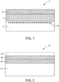
- a silicon on insulator structure 2 comprising a very high resistivity silicon wafer 4 , a buried oxide (BOX) layer 6 , and a silicon device layer 10 .
- Such a substrate is prone to formation of high conductivity charge inversion or accumulation layers 12 at the BOX/handle interface causing generation of free carriers (electrons or holes), which reduce the effective resistivity of the substrate and give rise to parasitic power losses and device nonlinearity when the devices are operated at RF frequencies.
- These inversion/accumulation layers can be due to BOX fixed charge, oxide trapped charge, interface trapped charge, and even DC bias applied to the devices themselves.
- a method is required therefore to trap the charge in any induced inversion or accumulation layers so that the high resistivity of the substrate is maintained even in the very near surface region.
- CTL charge trapping layers
- BOX buried oxide
- one method of creating a semiconductor-on-insulator structure 20 is based on depositing an undoped polycrystalline silicon film 28 on a silicon substrate having high resistivity 22 and then forming a stack of oxide 24 and top silicon layer 26 on it.
- a polycrystalline silicon layer 28 acts as a high defectivity layer between the silicon substrate 22 and the buried oxide layer 24 . See FIG. 2 , which depicts a polycrystalline silicon film for use as a charge trapping layer 28 between a high resistivity substrate 22 and the buried oxide layer 24 in a silicon-on-insulator structure 20 .
- An alternative method is the implantation of heavy ions to create a near surface damage layer. Devices, such as radiofrequency devices, are built in the top silicon layer 26 .
- Raskin "New substrate passivation method dedicated to high resistivity SOI wafer fabrication with increased substrate resistivity," IEEE Electron Device Letters, vol. 26, no. 11, pp.805-807, 2005 ; D. Lederer, B. Aspar, C. Laghaé and J.-P. Raskin, "Performance of RF passive structures and SOI MOSFETs transferred on a passivated HR SOI substrate," IEEE International SOI Conference, pp. 29-30, 2006 ; and Daniel C. Kerret al. "Identification of RF harmonic distortion on Si substrates and its reduction using a trap-rich layer", Silicon Monolithic Integrated Circuits in RF Systems, 2008 . SiRF 2008 (IEEE Topical Meeting), pp. 151-154, 2008 .
- US 2005153524 relates to integrated circuit (IC) structures and processes, and specifically to an efficient fabrication method of a strained silicon layer on an insulator, yielding a strained silicon-on-insulator (SSOI) structure that is useful for high speed device fabrication.
- IC integrated circuit
- SOI strained silicon-on-insulator
- the present invention is directed to a multilayer structure comprising: a single crystal semiconductor handle substrate comprising two major, generally parallel surfaces, one of which is a front surface of the single crystal semiconductor handle substrate and the other of which is a back surface of the single crystal semiconductor handle substrate, a circumferential edge joining the front and back surfaces of the single crystal semiconductor handle substrate, a central plane between the front surface and the back surface of the single crystal semiconductor handle substrate, and a bulk region between the front and back surfaces of the single crystal semiconductor handle substrate, wherein the single crystal semiconductor handle substrate has a minimum bulk region resistivity of at least 3000 Ohm-cm; a relaxed semiconductor layer comprising germanium, the relaxed semiconductor layer in interfacial contact with the front surface of the single crystal semiconductor handle substrate; a polycrystalline silicon charge trapping layer in interfacial contact with the relaxed semiconductor layer; a dielectric layer in interfacial contact with the polycrystalline silicon charge trapping layer; and a single crystal semiconductor device layer in interfacial contact with the dielectric layer.
- the present invention is further directed to a method of preparing a multilayer structure.
- the method comprises: forming a semiconductor layer to be in interfacial contact with a front surface of a single crystal semiconductor handle substrate, the single crystal semiconductor handle substrate comprising two major, generally parallel surfaces, one of which is the front surface of the single crystal semiconductor handle substrate and the other of which is a back surface of the single crystal semiconductor handle substrate, a circumferential edge joining the front and back surfaces of the single crystal semiconductor handle substrate, a central plane between the front surface and the back surface of the single crystal semiconductor handle substrate, and a bulk region between the front and back surfaces of the single crystal semiconductor handle substrate, wherein the single crystal semiconductor handle substrate has a minimum bulk region resistivity of at least 3000 Ohm-cm, and further wherein the semiconductor layer comprises germanium in a molar percent of germanium of at least 20 molar %; annealing the single crystal semiconductor handle substrate having the semiconductor layer in interfacial contact with the front surface of the single crystal semiconductor handle substrate for a temperature and a
- a method for producing a charge trapping layer on a single crystal semiconductor handle substrate, e.g., a single crystal semiconductor handle wafer.
- the single crystal semiconductor handle substrate e.g., a single crystal semiconductor handle wafer, comprising the charge trapping layer is useful in the production of a semiconductor-on-insulator (e.g., silicon-on-insulator) structure.
- the charge trapping layer in the single crystal semiconductor handle substrate e.g., a single crystal semiconductor handle wafer, is formed at the region near the oxide interface.
- the method of the present invention provides a highly defective charge trapping layer that is stable against thermal processing, such as subsequent thermal process steps of semiconductor-on-insulator substrate and device manufacture.
- the present invention is directed to a method of forming a semiconductor-on-insulator structure (e.g., silicon-on-insulator (SOI)) suitable for radio frequency (RF) device applications.
- a semiconductor-on-insulator structure comprises a device layer, a buried oxide layer, and a high resistivity silicon handle wafer. Additionally, the high resistivity handle also contains a polycrystalline silicon layer capable of trapping charges formed on the handle surface next to the interface of BOX layer and handle wafer of the SOI structure.
- a fully relaxed layer of high concentration SiGe or pure Ge is formed between the high resistivity handle wafer and polycrystalline silicon charge trapping layer to provide dislocation network preventing re-crystallization of the polycrystalline silicon charge trapping layer during the high temperature process steps involved in SOI manufacture.
- the present invention is directed to a method of forming a high resistivity single crystal semiconductor handle substrate with an improved immunity against formation of an inversion layer.
- the high resistivity single crystal semiconductor handle substrate is prepared to have a high concentration of Germanium at the BOX/Substrate interface. Germanium exhibits extremely poor electron mobility at the interfaces with oxides. Additionally, the Ge/SiO 2 interface has high interface defects which act as charge traps. In the result, the formation on the N-type inversion layer is suppressed. Finally, even if an N-type inversion layer forms, the conductivity through the Ge layer is low due to the poor electron mobility. Consequently, RF devices made using the single crystal semiconductor handle substrate comprising the Ge layer have improved performance.
- the substrates for use in the present invention include a semiconductor handle substrate, e.g., a single crystal semiconductor handle wafer and a semiconductor donor substrate, e.g., a single crystal semiconductor donor wafer.
- the semiconductor device layer in a semiconductor-on-insulator composite structure is derived from the semiconductor donor substrate, e.g., a single crystal semiconductor donor wafer.
- the semiconductor device layer may be transferred onto the semiconductor handle substrate by wafer thinning techniques such as etching a semiconductor donor substrate or by cleaving a semiconductor donor substrate comprising a damage plane.
- the single crystal semiconductor handle wafer and single crystal semiconductor donor wafer comprise two major, generally parallel surfaces. One of the parallel surfaces is a front surface of the substrate, and the other parallel surface is a back surface of the substrate.
- the substrates comprise a circumferential edge joining the front and back surfaces, and a central plane between the front and back surfaces.
- the substrates additionally comprise an imaginary central axis perpendicular to the central plane and a radial length that extends from the central axis to the circumferential edge.
- semiconductor substrates e.g., silicon wafers
- TTV total thickness variation
- warp warp
- bow the midpoint between every point on the front surface and every point on the back surface may not precisely fall within a plane.
- the TTV, warp, and bow are typically so slight that to a close approximation the midpoints can be said to fall within an imaginary central plane which is approximately equidistant between the front and back surfaces.
- a surface is referred to as a "front surface” or a “back surface” merely for convenience and generally to distinguish the surface upon which the operations of method of the present invention are performed.
- a "front surface” of a single crystal semiconductor handle substrate e.g., a single crystal silicon handle wafer
- a single crystal semiconductor handle substrate refers to the major surface of the substrate that becomes an interior surface of the bonded structure. It is upon this front surface that the charge trapping layer is formed.
- a "back surface” of a single crystal semiconductor handle substrate e.g., a handle wafer, refers to the major surface that becomes an exterior surface of the bonded structure.
- a "front surface" of a single crystal semiconductor donor substrate refers to the major surface of the single crystal semiconductor donor substrate that becomes an interior surface of the bonded structure.
- the front surface of a single crystal semiconductor donor substrate often comprises a dielectric layer, e.g., a silicon dioxide layer, which forms the buried oxide (BOX) layer in the final structure.
- a "back surface” of a single crystal semiconductor donor substrate e.g., a single crystal silicon donor wafer, refers to the major surface that becomes an exterior surface of the bonded structure.
- the single crystal semiconductor donor substrate forms the semiconductor device layer of the semiconductor-on-insulator (e.g., silicon-on-insulator) composite structure.
- the single crystal semiconductor handle substrate and the single crystal semiconductor donor substrate may be single crystal semiconductor wafers.
- the semiconductor wafers comprise a material selected from the group consisting of silicon, silicon carbide, silicon germanium, gallium arsenide, gallium nitride, indium phosphide, indium gallium arsenide, germanium, and combinations thereof.
- the semiconductor wafers comprise a semiconductor material selected from among silicon, silicon carbide, and silicon germanium.
- the single crystal semiconductor wafers, e.g., the single crystal silicon handle wafer and single crystal silicon donor wafer, of the present invention typically have a nominal diameter of at least 150 mm, at least 200 mm, at least 300 mm, or at least 450 mm.
- Wafer thicknesses may vary from 250 micrometers to 1500 micrometers, such as between 300 micrometers and 1000 micrometers, suitably within the range of 500 micrometers to 1000 micrometers. In some specific embodiments, the wafer thickness may be 725 micrometers.
- the single crystal semiconductor wafers comprise single crystal silicon wafers which have been sliced from a single crystal ingot grown in accordance with conventional Czochralski crystal growing methods or float zone growing methods.
- Czochralski crystal growing methods or float zone growing methods.
- Such methods, as well as standard silicon slicing, lapping, etching, and polishing techniques are disclosed, for example, in F. Shimura, Semiconductor Silicon Crystal Technology, Academic Press, 1989 , and Silicon Chemical Etching, (J. Grabmaier ed.) Springer-Verlag, N.Y., 1982 .
- the wafers are polished and cleaned by standard methods known to those skilled in the art. See, for example, W.C. O'Mara et al., Handbook of Semiconductor Silicon Technology, Noyes Publications .
- the wafers can be cleaned, for example, in a standard SC1/ SC2 solution.
- the single crystal silicon wafers of the present invention are single crystal silicon wafers which have been sliced from a single crystal ingot grown in accordance with conventional Czochralski ("Cz") crystal growing methods, typically having a nominal diameter of at least 150 mm, at least 200 mm, at least 300 mm, or at least 450 mm.
- both the single crystal silicon handle wafer and the single crystal silicon donor wafer have mirror-polished front surface finishes that are free from surface defects, such as scratches, large particles, etc.
- Wafer thickness may vary from 250 micrometers to 1500 micrometers, such as between 300 micrometers and 1000 micrometers, suitably within the range of 500 micrometers to 1000 micrometers. In some specific embodiments, the wafer thickness may be 725 micrometers.
- the single crystal semiconductor wafers i.e., handle wafer and donor wafer, comprise interstitial oxygen in concentrations that are generally achieved by the Czochralski-growth method.
- the semiconductor wafers comprise oxygen in a concentration between 4 PPMA and 18 PPMA.
- the semiconductor wafers comprise oxygen in a concentration between 10 PPMA and 35 PPMA.
- the single crystal silicon handle wafer comprises oxygen in a concentration of no greater than 10 PPMA. Interstitial oxygen may be measured according to SEMI MF 1188-1105.
- the semiconductor handle substrate e.g., a single crystal semiconductor handle substrate, such as a single crystal silicon handle wafer
- the semiconductor handle substrate has a relatively high minimum bulk resistivity.
- High resistivity wafers are generally sliced from single crystal ingots grown by the Czochralski method or float zone method.
- Cz-grown silicon wafers may be subjected to a thermal anneal at a temperature ranging from 600°C to 1000°C in order to annihilate thermal donors caused by oxygen that are incorporated during crystal growth.
- the single crystal semiconductor handle wafer has a minimum bulk resistivity of at least 3000 Ohm-cm, such as between 3000 Ohm-cm and 100,000 Ohm-cm, between 3000 Ohm-cm and 10,000 Ohm-cm, or between 3000 Ohm cm and 5,000 Ohm-cm.
- Methods for preparing high resistivity wafers are known in the art, and such high resistivity wafers may be obtained from commercial suppliers, such as SunEdison Semiconductor Ltd. (St. Peters, MO; formerly MEMC Electronic Materials, Inc.).
- the single crystal semiconductor handle substrate comprises a p-type or an n-type dopant. Suitable dopants include Arsenic, Phosphorus, and Boron. In some embodiments, the single crystal semiconductor handle substrate comprises a p-type dopant. In some embodiments, the single crystal semiconductor handle substrate is a single crystal silicon wafer comprising a p-type dopant, such as boron. The boron dopant is present in a relatively low concentration, e.g., less than 1x10 14 atoms/cm 3 , preferably less than 1x10 13 atoms/cm 3 , so as to obtain high resistivity handle substrates.
- the single crystal semiconductor handle wafer surface could be intentionally damaged by a sound blasting process or by a caustic etch.
- the front surface of the single crystal semiconductor handle wafer may be oxidized by conventional oxidation methods, such as thermal oxidation (in which some portion of the single crystal semiconductor material will be consumed) and/or CVD oxide deposition prior to deposition of the charge trapping layer.
- a polycrystalline silicon charge trapping layer is deposited in interfacial contact with the relaxed semiconductor layer.
- Polycrystalline material denotes a material comprising small crystals having random crystal orientations. Polycrystalline grains may be as small in size as 20 nanometers. According to the method of the present invention, the smaller the crystal grain size of polycrystalline material deposited the higher the defectivity in the charge trapping layer.
- Amorphous material comprises a non-crystalline allotropic forms of silicon and germanium, which lacks short range and long range order. Grains having crystallinity over no more than 10 nanometers may also be considered essentially amorphous.
- Polycrystalline and amorphous material may be deposited using metalorganic chemical vapor deposition (MOCVD), physical vapor deposition (PVD), chemical vapor deposition (CVD), low pressure chemical vapor deposition (LPCVD), plasma enhanced chemical vapor deposition (PECVD), or molecular beam epitaxy (MBE).
- MOCVD metalorganic chemical vapor deposition
- PVD physical vapor deposition
- CVD chemical vapor deposition
- LPCVD low pressure chemical vapor deposition
- PECVD plasma enhanced chemical vapor deposition
- MBE molecular beam epitaxy
- Silicon germanium comprises an alloy of silicon germanium in any molar ratio of silicon and germanium.
- the semiconductor material comprising silicon and germanium may be doped with carbon.
- the charge trapping layer has a resistivity at least 1000 Ohm-cm, or at least 3000 Ohm-cm, such as between 1000 Ohm-cm and 100,000 Ohm-cm, between 1000 Ohm-cm and 10,000 Ohm-cm, between 2000 Ohm-cm and 10,000 Ohm-cm, between 3000 Ohm-cm and 10,000 Ohm-cm, or between 3000 Ohm cm and 5,000 Ohm-cm.
- a relaxed semiconductor layer comprising germanium is formed on the single crystal semiconductor handle substrate, the relaxed semiconductor layer being in interfacial contact with the front surface of the single crystal semiconductor handle substrate.
- the semiconductor material comprises silicon and germanium wherein the molar percent of germanium is at least 20 molar %. In some embodiments, the semiconductor material comprises silicon and germanium, wherein the molar percent of germanium is at least 50 molar %, at least 90 molar %, such as at least 99.9 molar %. In some embodiments, the semiconductor material consists essentially of germanium.
- a semiconductor material that consists essentially of germanium is formed by deposition using germanium precursors.
- the final semiconductor material consisting essentially of germanium comprises no more than 0.1 molar %, preferably no more than 0.01 molar %, trace impurities that preferably do not affect the physical and electrical properties of the germanium layer.
- the semiconductor material comprising silicon, germanium, or a combination of silicon and germanium may be deposited to a thickness greater than the critical thickness, i.e., the thickness beyond which the elastic strain due to lattice mismatch may be relaxed during a strain relaxing thermal anneal.
- the critical thickness may depend upon the concentration of germanium. The lower the germanium concentration, the larger the critical thickness.
- the deposited semiconductor layer comprising silicon and germanium having at least 20 molar % Ge is generally deposited to a thickness between 1 nanometer and 3000 nanometers, such as between 10 nanometers and 3000 nanometers, such as between 10 nanometers and 1000 nanometers. As the Ge concentration increases, the critical thickness may be less. For a 100 molar % Ge layer, the thickness is between 0.1 nanometers and 1000 nanometers, such as between 1 nanometer and 1000 nanometers, or between 10 nanometer and 500 nanometers.
- the semiconductor layer comprises silicon and germanium, wherein the germanium content is at least 5 molar %. In some embodiments, the semiconductor layer comprises silicon and germanium, wherein the germanium content is no more than 20 molar %, such as between 5 molar % and 20 molar %. In some embodiments, the germanium enriched silicon layer is deposited on the front surface of the single crystal semiconductor handle substrate acts alone as the charge trapping layer. At lower concentrations of Ge, the layer may be more thickly deposited to ensure relaxation, such as between 5 nanometers and 4000 nanometers, or between 10 nanometers and 3000 nanometers, or between 20 nanometers and 1000 nanometers.
- the germanium enriched silicon layer may comprise carbon, in an amount between 0.1 molar % and 5 molar %, such as between 0.5 molar % and 1 molar %.
- the layer may have a thickness between 10 nanometers and 8000 nanometers, or between 10 nanometers and 6000 nanometers, or between 20 nanometers and 3000 nanometers.
- the material for deposition onto the front surface of the single crystal semiconductor handle wafer to thereby form the charge trapping layer may be deposited by means known in the art.
- the semiconductor material may be deposited using epitaxial deposition, metalorganic chemical vapor deposition (MOCVD), physical vapor deposition (PVD), chemical vapor deposition (CVD), low pressure chemical vapor deposition (LPCVD), plasma enhanced chemical vapor deposition (PECVD), or molecular beam epitaxy (MBE).
- MOCVD metalorganic chemical vapor deposition
- PVD physical vapor deposition
- CVD chemical vapor deposition
- LPCVD low pressure chemical vapor deposition
- PECVD plasma enhanced chemical vapor deposition
- MBE molecular beam epitaxy
- Silicon precursors for LPCVD or PECVD include methyl silane, silicon tetrahydride (silane), trisilane, disilane, pentasilane, neopentasilane, tetrasilane, dichlorosilane (SiH 2 Cl 2 ), silicon tetrachloride (SiCl 4 ), among others.
- polycrystalline silicon may be deposited onto the surface oxidation layer by pyrolyzing silane (SiH 4 ) in a temperature range between 550°C and 690°C, such as between 580°C and 650°C.
- the chamber pressure may range from 70 to 400 mTorr.
- Amorphous silicon may be deposited by plasma enhanced chemical vapor deposition (PECVD) at temperatures generally ranging between 75°C and 300°C.
- Silicon germanium particularly amorphous silicon germanium, may be deposited at temperatures up to 300°C by chemical vapor deposition by including organogermanium compounds, such as isobutylgermane, alkylgermanium trichlorides, and dimethylaminogermanium trichloride.
- Silicon doped with carbon may be deposited by thermal plasma chemical vapor deposition in epitaxial reactors using precursors such as silicon tetrachloride and methane. Suitable carbon precursors for CVD or PECVD include methylsilane, methane, ethane, ethylene, among others.
- methylsilane is a particularly preferred precursor since it provides both carbon and silicon.
- the preferred precursors include silane and methane.
- the single crystal semiconductor handle substrate may be annealed at a temperature and duration sufficient to at least partially relax, or fully relax the semiconductor material comprising germanium.
- Elastic strain begins to relax at elevated temperatures.
- the relaxation is realized by generating misfit dislocations at the interface between the layer and the high resistivity semiconductor handle substrate.
- a high density of misfit dislocations and threading dislocations are present, i.e., on the order of 1x10 5 to 1x10 10 per cm 2 .
- the relaxation anneal may occur at a temperature in excess of 600°C, such as between 700°C and 900°C.
- the relaxation anneal may occur for a duration between 1 second and 1 hour, such as between 10 seconds and 30 minutes, such as between 1 minute and 30 minutes.
- a polycrystalline silicon charge trapping layer is deposited on the relaxed layer of semiconductor material comprising germanium.
- the polycrystalline silicon charge trapping layer may be deposited as described above, using suitable silicon precursors and conditions.
- the combination of the relaxed layer of semiconductor material comprising germanium and the polycrystalline silicon charge trapping layer acts as a charge trapping layer.
- a fully relaxed layer comprising SiGe or consisting essentially of Ge is formed between the high resistivity handle wafer and polycrystalline silicon charge trapping layer to provide dislocation network preventing re-crystallization of the polycrystalline silicon charge trapping layer during the high temperature process steps involved in SOI manufacture.
- the polycrystalline silicon charge trapping layer may be deposited to a thickness between 0.5 micrometer and 3 micrometers, or between 1 micrometer and 3 micrometers.
- an oxide film is formed on top of the deposited charge trapping layer. This may be accomplished by means known in the art, such as thermal oxidation (in which some portion of the deposited semiconductor material film will be consumed) and/or CVD oxide deposition.
- the charge trapping layer may be thermally oxidized (in which some portion of the deposited semiconductor material film will be consumed) or the silicon dioxide film may be grown by CVD oxide deposition.
- the charge trapping layer deposited on the front surface of the single crystal semiconductor handle substrate may be thermally oxidized in a furnace such as an ASM A400.
- the temperature may range from 750°C to 1200°C in an oxidizing ambient.
- the oxidizing ambient atmosphere can be a mixture of inert gas, such as Ar or N 2 , and O 2 .
- the oxygen content may vary from 1 to 10 percent, or higher.
- the oxidizing ambient atmosphere may be up to 100% (a "dry oxidation").
- semiconductor handle wafers may be loaded into a vertical furnace, such as an A400. The temperature is ramped to the oxidizing temperature with a mixture of N 2 and O 2 . After the desired oxide thickness has been obtained, the O 2 is turned off and the furnace temperature is reduced and wafers are unloaded from the furnace.
- the atmosphere may comprise nitrogen alone or a combination of oxygen and nitrogen, and the temperature may be increased to a temperature between 1100°C and 1400°C.
- An alternative nitrogen source is ammonia.
- the charge trapping layer may be oxidized for a duration sufficient to provide an oxide layer of at least 0.01 micrometers thick, or at least 0.05 micrometers thick, such as between 0.05 micrometers and 4 micrometers, such as between 0.1 micrometers and 2 micrometers, or between 0.2 micrometers and 0.4 micrometers,
- Oxidation of a film comprising silicon germanium or germanium may cause Ge to become enriched at the interface of the oxide layer and the front surface of the single crystal silicon handle substrate. This gives rise to very high concentration of Ge between the oxide and the substrate.
- the oxidation of Si then proceeds by Si diffusing though the Ge-rich layer. In this way, the desired structure of the SOI wafer is formed.
- the oxidation process additionally oxidizes the back surface of the single crystal semiconductor handle wafer, which advantageously reduces warp and bow potentially caused by the different coefficients of thermal expansion of silicon and silicon dioxide.
- CMP chemical mechanical polishing
- a single crystal semiconductor donor substrate such as a single crystal semiconductor wafer of a material that is conventionally used in preparation of multilayer semiconductor structures, e.g., a single crystal silicon donor wafer, that has been etched and polished and optionally oxidized, is subjecte
- the front surface of the single crystal semiconductor donor substrate may be thermally oxidized (in which some portion of the semiconductor material will be consumed) or the silicon dioxide film may be grown by CVD oxide deposition.
- the single crystal semiconductor donor substrate e.g., a single crystal silicon donor wafer
- the temperature may range from 750°C to 1200°C in an oxidizing ambient.
- the oxidizing ambient atmosphere can be a mixture of inert gas, such as Ar or N 2 , and O 2 .
- the oxygen content may vary from 1 to 10 percent, or higher.
- the oxidizing ambient atmosphere may be up to 100% (a "dry oxidation").
- semiconductor donor wafers may be loaded into a vertical furnace, such as an A400.
- the temperature is ramped to the oxidizing temperature with a mixture of N 2 and O 2 .
- the O 2 is turned off and the furnace temperature is reduced and wafers are unloaded from the furnace.
- the donor substrates are oxidized to provide an oxide layer on the front surface layer of at least 1 nanometer thick, such as between 0.01 micrometers and 10 micrometers, such as between 0.01 micrometers and 2 micrometers, or between 0.1 micrometers and 1 micrometers.
- the oxidation process additionally oxidizes the back surface of the donor substrate, which advantageously reduces warp and bow potentially caused by the different coefficients of thermal expansion of silicon and silicon dioxide.
- Ion implantation of the single crystal semiconductor donor substrate may be carried out in a commercially available instrument, such as an Applied Materials Quantum H.
- Implanted ions include He, H, H2, or combinations thereof.
- Ion implantation is carried out as a density and duration sufficient to form a damage layer in the semiconductor donor substrate.
- Implant density may range from 10 12 ions/cm 2 to 10 17 ions/cm 2 , such as from 10 14 ions/cm 2 to 10 17 ions/cm 2 .
- Implant energies may range from 1 keV to 3,000 keV, such as from 10 keV to 3,000 keV.
- the single crystal semiconductor donor wafers e.g., single crystal silicon donor wafers
- the clean could include a Piranha clean followed by a DI water rinse and SC1/SC2 cleans.
- the single crystal semiconductor donor substrate having an ion implant region therein formed by helium ion and/or hydrogen ion implant is annealed at a temperature sufficient to form a thermally activated cleave plane in the single crystal semiconductor donor substrate.
- a suitable tool might be a simple Box furnace, such as a Blue M model.
- the ion implanted single crystal semiconductor donor substrate is annealed at a temperature of from 200°C to 350°C, from 225°C to 325°C, preferably 300°C. Thermal annealing may occur for a duration of from 2 hours to 10 hours, such as from 2 hours to 8 hours. Thermal annealing within these temperatures ranges is sufficient to form a thermally activated cleave plane. After the thermal anneal to activate the cleave plane, the single crystal semiconductor donor substrate surface is preferably cleaned.
- the ion-implanted and optionally cleaned and optionally annealed single crystal semiconductor donor substrate is subjected to oxygen plasma and/or nitrogen plasma surface activation.
- the oxygen plasma surface activation tool is a commercially available tool, such as those available from EV Group, such as EVG®810LT Low Temp Plasma Activation System.
- the ion-implanted and optionally cleaned single crystal semiconductor donor wafer is loaded into the chamber.
- the chamber is evacuated and backfilled with O 2 to a pressure less than atmospheric to thereby create the plasma.
- the single crystal semiconductor donor wafer is exposed to this plasma for the desired time, which may range from 1 second to 120 seconds.
- Oxygen plasma surface oxidation is performed in order to render the front surface of the single crystal semiconductor donor substrate hydrophilic and amenable to bonding to a single crystal semiconductor handle substrate prepared according to the method described above.
- the hydrophilic front surface layer of the single crystal semiconductor donor substrate and the front surface of the single crystal semiconductor handle substrate, which comprises the charge trapping layer and may further be optionally oxidized, are next brought into intimate contact to thereby form a bonded structure. Since the mechanical bond is relatively weak, the bonded structure is further annealed to solidify the bond between the donor wafer and the handle wafer. In some embodiments of the present invention, the bonded structure is annealed at a temperature sufficient to form a thermally activated cleave plane in the single crystal semiconductor donor substrate.
- An example of a suitable tool might be a simple Box furnace, such as a Blue M model.
- the bonded structure is annealed at a temperature of from 200°C to 350°C, from 225°C to 325°C, preferably 300°C. Thermal annealing may occur for a duration of from 0.5 hours to 10 hours, preferably a duration of 2 hours. Thermal annealing within these temperatures ranges is sufficient to form a thermally activated cleave plane. After the thermal anneal to activate the cleave plane, the bonded structure may be cleaved.
- the bond between the single crystal semiconductor donor substrate and the single crystal semiconductor handle substrate is strong enough to initiate layer transfer via cleaving the bonded structure at the cleave plane.
- Cleaving may occur according to techniques known in the art.
- the bonded structure may be placed in a conventional cleave station affixed to stationary suction cups on one side and affixed by additional suction cups on a hinged arm on the other side.
- a crack is initiated near the suction cup attachment and the movable arm pivots the hinge cleaving the wafer apart.
- Cleaving removes a portion of the semiconductor donor wafer, thereby leaving a semiconductor device layer, preferably a silicon device layer, on the semiconductor-on-insulator composite structure.
- the cleaved structure may be subjected to a high temperature anneal in order to further strengthen the bond between the transferred device layer and the single crystal semiconductor handle substrate.
- a suitable tool might be a vertical furnace, such as an ASM A400.
- the bonded structure is annealed at a temperature of from 1000°C to 1200°C, preferably at 1000°C. Thermal annealing may occur for a duration of from 0.5 hours to 8 hours, preferably a duration of 4 hours. Thermal annealing within these temperatures ranges is sufficient to strengthen the bond between the transferred device layer and the single crystal semiconductor handle substrate.
- the bonded structure may be subjected to a cleaning process designed to remove thin thermal oxide and clean particulates from the surface.
- the single crystal semiconductor donor wafer may be brought to the desired thickness and smoothness by subjecting to a vapor phase HCl etch process in a horizontal flow single wafer epitaxial reactor using H2 as a carrier gas.
- the thickness of the device layer may be between 1 nanometer and 100 micrometers, such as between 10 nanometers and 50 micrometers.
- an epitaxial layer may be deposited on the transferred device layer.
- the finished SOI wafer comprises the semiconductor handle substrate, the charge trapping layer, the dielectric layer (e.g., buried oxide layer), and the semiconductor device layer, may then be subjected to end of line metrology inspections and cleaned a final time using typical SC1-SC2 process.
- the dielectric layer e.g., buried oxide layer
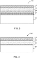
- a semiconductor-on-insulator structure 100 e.g., a silicon-on-insulator wafer according to some embodiments of the invention is depicted.
- the semiconductor-on-insulator structure 100 e.g., a silicon-on-insulator wafer comprises a high resistivity semiconductor substrate 102 , e.g., a high resistivity single crystal silicon substrate.
- a relaxed SiGe or Ge layer 104 is formed in interfacial contact with the front surface of the high resistivity semiconductor substrate 102 , e.g., a high resistivity single crystal silicon substrate.
- a polycrystalline silicon charge trapping layer 106 is formed in interfacial contact with the relaxed SiGe or Ge layer 104 .
- a buried oxide layer 108 is located between the relaxed SiGe or Ge layer 104 and a single crystal semiconductor device layer 110 , e.g., a silicon device layer.
- the buried oxide layer 108 may be formed from oxidized portions of the relaxed SiGe or Ge layer 104 and the single crystal semiconductor device layer 110 , e.g., a silicon device layer.
- a semiconductor-on-insulator structure 200 e.g., a silicon-on-insulator wafer according to some embodiments of the invention is depicted.
- the semiconductor-on-insulator structure 200 e.g., a silicon-on-insulator wafer comprises a high resistivity semiconductor substrate 202 , e.g., a high resistivity single crystal silicon substrate.
- a Ge-rich layer 204 is formed in interfacial contact with the front surface of the high resistivity semiconductor substrate 202 , e.g., a high resistivity single crystal silicon substrate.
- a buried oxide layer 208 is located between Ge-rich layer 204 and a single crystal semiconductor device layer 210 , e.g., a silicon device layer.
- the buried oxide layer 208 may be formed from oxidized portions of the Ge-rich layer 204 and the single crystal semiconductor device layer 110 , e.g., a silicon device layer.
Landscapes
- Recrystallisation Techniques (AREA)
- Crystals, And After-Treatments Of Crystals (AREA)
- Element Separation (AREA)
Priority Applications (2)
| Application Number | Priority Date | Filing Date | Title |
|---|---|---|---|
| EP22213747.3A EP4170705A3 (en) | 2014-11-18 | 2015-11-16 | High resistivity semiconductor-on-insulator wafer and a method of manufacturing |
| EP19185201.1A EP3573094B1 (en) | 2014-11-18 | 2015-11-16 | High resistivity semiconductor-on-insulator wafer and a method of manufacturing |
Applications Claiming Priority (2)
| Application Number | Priority Date | Filing Date | Title |
|---|---|---|---|
| US201462081352P | 2014-11-18 | 2014-11-18 | |
| PCT/US2015/060854 WO2016081356A1 (en) | 2014-11-18 | 2015-11-16 | High resistivity semiconductor-on-insulator wafer and a method of manufacturing |
Related Child Applications (3)
| Application Number | Title | Priority Date | Filing Date |
|---|---|---|---|
| EP19185201.1A Division EP3573094B1 (en) | 2014-11-18 | 2015-11-16 | High resistivity semiconductor-on-insulator wafer and a method of manufacturing |
| EP19185201.1A Division-Into EP3573094B1 (en) | 2014-11-18 | 2015-11-16 | High resistivity semiconductor-on-insulator wafer and a method of manufacturing |
| EP22213747.3A Division EP4170705A3 (en) | 2014-11-18 | 2015-11-16 | High resistivity semiconductor-on-insulator wafer and a method of manufacturing |
Publications (2)
| Publication Number | Publication Date |
|---|---|
| EP3221885A1 EP3221885A1 (en) | 2017-09-27 |
| EP3221885B1 true EP3221885B1 (en) | 2019-10-23 |
Family
ID=54705879
Family Applications (3)
| Application Number | Title | Priority Date | Filing Date |
|---|---|---|---|
| EP15801615.4A Active EP3221885B1 (en) | 2014-11-18 | 2015-11-16 | High resistivity semiconductor-on-insulator wafer and a method of manufacturing |
| EP19185201.1A Active EP3573094B1 (en) | 2014-11-18 | 2015-11-16 | High resistivity semiconductor-on-insulator wafer and a method of manufacturing |
| EP22213747.3A Pending EP4170705A3 (en) | 2014-11-18 | 2015-11-16 | High resistivity semiconductor-on-insulator wafer and a method of manufacturing |
Family Applications After (2)
| Application Number | Title | Priority Date | Filing Date |
|---|---|---|---|
| EP19185201.1A Active EP3573094B1 (en) | 2014-11-18 | 2015-11-16 | High resistivity semiconductor-on-insulator wafer and a method of manufacturing |
| EP22213747.3A Pending EP4170705A3 (en) | 2014-11-18 | 2015-11-16 | High resistivity semiconductor-on-insulator wafer and a method of manufacturing |
Country Status (4)
| Country | Link |
|---|---|
| US (3) | US10483152B2 (enExample) |
| EP (3) | EP3221885B1 (enExample) |
| JP (4) | JP6726180B2 (enExample) |
| WO (1) | WO2016081356A1 (enExample) |
Families Citing this family (14)
| Publication number | Priority date | Publication date | Assignee | Title |
|---|---|---|---|---|
| JP6447439B2 (ja) * | 2015-09-28 | 2019-01-09 | 信越半導体株式会社 | 貼り合わせsoiウェーハの製造方法 |
| US10622247B2 (en) * | 2016-02-19 | 2020-04-14 | Globalwafers Co., Ltd. | Semiconductor on insulator structure comprising a buried high resistivity layer |
| US10825681B2 (en) * | 2016-08-13 | 2020-11-03 | Applied Materials, Inc. | 3D CTF integration using hybrid charge trap layer of sin and self aligned SiGe nanodot |
| JP6831911B2 (ja) * | 2016-10-26 | 2021-02-17 | グローバルウェーハズ カンパニー リミテッドGlobalWafers Co.,Ltd. | 向上した電荷捕獲効率を有する高抵抗率シリコンオンインシュレータ基板 |
| JP6801105B2 (ja) * | 2016-12-05 | 2020-12-16 | グローバルウェーハズ カンパニー リミテッドGlobalWafers Co.,Ltd. | 高抵抗シリコンオンインシュレータ構造及びその製造方法 |
| US10943813B2 (en) | 2018-07-13 | 2021-03-09 | Globalwafers Co., Ltd. | Radio frequency silicon on insulator wafer platform with superior performance, stability, and manufacturability |
| CN110943066A (zh) * | 2018-09-21 | 2020-03-31 | 联华电子股份有限公司 | 具有高电阻晶片的半导体结构及高电阻晶片的接合方法 |
| FR3091618B1 (fr) * | 2019-01-09 | 2021-09-24 | Soitec Silicon On Insulator | Procédé de fabrication d’un substrat receveur pour une structure de type semi-conducteur sur isolant pour applications radiofrequences et procédé de fabrication d’une telle structure |
| FR3098985B1 (fr) * | 2019-07-15 | 2022-04-08 | Soitec Silicon On Insulator | Procédé de collage hydrophile de substrats |
| US11296190B2 (en) * | 2020-01-15 | 2022-04-05 | Globalfoundries U.S. Inc. | Field effect transistors with back gate contact and buried high resistivity layer |
| US11715886B2 (en) | 2020-05-08 | 2023-08-01 | Mobix Labs, Inc. | Low-cost, IPD and laminate based antenna array module |
| EP4287239A1 (en) * | 2022-06-02 | 2023-12-06 | Imec VZW | A low loss semiconductor substrate |
| CN116487242A (zh) * | 2022-12-15 | 2023-07-25 | 苏州华太电子技术股份有限公司 | 抑制射频器件欧姆损耗的方法及射频器件 |
| CN119108402A (zh) * | 2023-06-08 | 2024-12-10 | 无锡晶湛半导体有限公司 | 一种复合衬底及其制造方法 |
Family Cites Families (90)
| Publication number | Priority date | Publication date | Assignee | Title |
|---|---|---|---|---|
| US4501060A (en) | 1983-01-24 | 1985-02-26 | At&T Bell Laboratories | Dielectrically isolated semiconductor devices |
| US4755865A (en) | 1986-01-21 | 1988-07-05 | Motorola Inc. | Means for stabilizing polycrystalline semiconductor layers |
| JPH0648686B2 (ja) | 1988-03-30 | 1994-06-22 | 新日本製鐵株式会社 | ゲッタリング能力の優れたシリコンウェーハおよびその製造方法 |
| JPH06105691B2 (ja) | 1988-09-29 | 1994-12-21 | 株式会社富士電機総合研究所 | 炭素添加非晶質シリコン薄膜の製造方法 |
| JP2617798B2 (ja) | 1989-09-22 | 1997-06-04 | 三菱電機株式会社 | 積層型半導体装置およびその製造方法 |
| JP3217089B2 (ja) * | 1991-08-23 | 2001-10-09 | 富士通株式会社 | Soiウェハおよびその製造方法 |
| US5461250A (en) * | 1992-08-10 | 1995-10-24 | International Business Machines Corporation | SiGe thin film or SOI MOSFET and method for making the same |
| US6043138A (en) | 1996-09-16 | 2000-03-28 | Advanced Micro Devices, Inc. | Multi-step polysilicon deposition process for boron penetration inhibition |
| US5783469A (en) | 1996-12-10 | 1998-07-21 | Advanced Micro Devices, Inc. | Method for making nitrogenated gate structure for improved transistor performance |
| FR2765393B1 (fr) * | 1997-06-25 | 2001-11-30 | France Telecom | Procede de gravure d'une couche de si1-xgex polycristallin ou d'un empilement d'une couche de si1-xgex polycristallin et d'une couche de si polycristallin, et son application a la microelectronique |
| US6068928A (en) | 1998-02-25 | 2000-05-30 | Siemens Aktiengesellschaft | Method for producing a polycrystalline silicon structure and polycrystalline silicon layer to be produced by the method |
| US6479166B1 (en) | 1998-10-06 | 2002-11-12 | Case Western Reserve University | Large area polysilicon films with predetermined stress characteristics and method for producing same |
| JP4313874B2 (ja) | 1999-02-02 | 2009-08-12 | キヤノン株式会社 | 基板の製造方法 |
| US6204205B1 (en) | 1999-07-06 | 2001-03-20 | Taiwan Semiconductor Manufacturing Company | Using H2anneal to improve the electrical characteristics of gate oxide |
| US6323108B1 (en) * | 1999-07-27 | 2001-11-27 | The United States Of America As Represented By The Secretary Of The Navy | Fabrication ultra-thin bonded semiconductor layers |
| US20020090758A1 (en) | 2000-09-19 | 2002-07-11 | Silicon Genesis Corporation | Method and resulting device for manufacturing for double gated transistors |
| JP4463957B2 (ja) | 2000-09-20 | 2010-05-19 | 信越半導体株式会社 | シリコンウエーハの製造方法およびシリコンウエーハ |
| US20050026432A1 (en) | 2001-04-17 | 2005-02-03 | Atwater Harry A. | Wafer bonded epitaxial templates for silicon heterostructures |
| US6562127B1 (en) | 2002-01-16 | 2003-05-13 | The United States Of America As Represented By The Secretary Of The Navy | Method of making mosaic array of thin semiconductor material of large substrates |
| US6562703B1 (en) * | 2002-03-13 | 2003-05-13 | Sharp Laboratories Of America, Inc. | Molecular hydrogen implantation method for forming a relaxed silicon germanium layer with high germanium content |
| US7074623B2 (en) | 2002-06-07 | 2006-07-11 | Amberwave Systems Corporation | Methods of forming strained-semiconductor-on-insulator finFET device structures |
| US6995430B2 (en) | 2002-06-07 | 2006-02-07 | Amberwave Systems Corporation | Strained-semiconductor-on-insulator device structures |
| US7057234B2 (en) | 2002-12-06 | 2006-06-06 | Cornell Research Foundation, Inc. | Scalable nano-transistor and memory using back-side trapping |
| EP1588416B1 (en) | 2003-01-07 | 2009-03-25 | S.O.I.Tec Silicon on Insulator Technologies | Recycling of a wafer comprising a multi-layer structure after taking-off a thin layer |
| US6995427B2 (en) | 2003-01-29 | 2006-02-07 | S.O.I.Tec Silicon On Insulator Technologies S.A. | Semiconductor structure for providing strained crystalline layer on insulator and method for fabricating same |
| JP4853990B2 (ja) | 2003-01-29 | 2012-01-11 | ソイテック | 絶縁体上に歪み結晶層を製造する方法、前記方法による半導体構造及び製造された半導体構造 |
| US7005160B2 (en) | 2003-04-24 | 2006-02-28 | Asm America, Inc. | Methods for depositing polycrystalline films with engineered grain structures |
| WO2005013326A2 (en) * | 2003-07-30 | 2005-02-10 | Asm America, Inc. | Epitaxial growth of relaxed silicon germanium layers |
| JPWO2005022610A1 (ja) * | 2003-09-01 | 2007-11-01 | 株式会社Sumco | 貼り合わせウェーハの製造方法 |
| US20070032040A1 (en) * | 2003-09-26 | 2007-02-08 | Dimitri Lederer | Method of manufacturing a multilayer semiconductor structure with reduced ohmic losses |
| US6992025B2 (en) * | 2004-01-12 | 2006-01-31 | Sharp Laboratories Of America, Inc. | Strained silicon on insulator from film transfer and relaxation by hydrogen implantation |
| US7018882B2 (en) * | 2004-03-23 | 2006-03-28 | Sharp Laboratories Of America, Inc. | Method to form local “silicon-on-nothing” or “silicon-on-insulator” wafers with tensile-strained silicon |
| US7279400B2 (en) | 2004-08-05 | 2007-10-09 | Sharp Laboratories Of America, Inc. | Method of fabricating single-layer and multi-layer single crystalline silicon and silicon devices on plastic using sacrificial glass |
| US7312487B2 (en) | 2004-08-16 | 2007-12-25 | International Business Machines Corporation | Three dimensional integrated circuit |
| DE102004041378B4 (de) | 2004-08-26 | 2010-07-08 | Siltronic Ag | Halbleiterscheibe mit Schichtstruktur mit geringem Warp und Bow sowie Verfahren zu ihrer Herstellung |
| GB0424290D0 (en) * | 2004-11-02 | 2004-12-01 | Koninkl Philips Electronics Nv | Method of growing a strained layer |
| US7476594B2 (en) | 2005-03-30 | 2009-01-13 | Cree, Inc. | Methods of fabricating silicon nitride regions in silicon carbide and resulting structures |
| FR2890489B1 (fr) | 2005-09-08 | 2008-03-07 | Soitec Silicon On Insulator | Procede de fabrication d'une heterostructure de type semi-conducteur sur isolant |
| JP2007214199A (ja) * | 2006-02-07 | 2007-08-23 | Canon Inc | 半導体基板及びその製造方法 |
| FR2897982B1 (fr) | 2006-02-27 | 2008-07-11 | Tracit Technologies Sa | Procede de fabrication des structures de type partiellement soi, comportant des zones reliant une couche superficielle et un substrat |
| US7936043B2 (en) * | 2006-03-17 | 2011-05-03 | Sychip Inc. | Integrated passive device substrates |
| FR2902233B1 (fr) | 2006-06-09 | 2008-10-17 | Soitec Silicon On Insulator | Procede de limitation de diffusion en mode lacunaire dans une heterostructure |
| FR2911430B1 (fr) | 2007-01-15 | 2009-04-17 | Soitec Silicon On Insulator | "procede de fabrication d'un substrat hybride" |
| CN101681807B (zh) | 2007-06-01 | 2012-03-14 | 株式会社半导体能源研究所 | 半导体器件的制造方法 |
| JP4445524B2 (ja) | 2007-06-26 | 2010-04-07 | 株式会社東芝 | 半導体記憶装置の製造方法 |
| JP2009016692A (ja) | 2007-07-06 | 2009-01-22 | Toshiba Corp | 半導体記憶装置の製造方法と半導体記憶装置 |
| US20090278233A1 (en) | 2007-07-26 | 2009-11-12 | Pinnington Thomas Henry | Bonded intermediate substrate and method of making same |
| US7915716B2 (en) | 2007-09-27 | 2011-03-29 | Stats Chippac Ltd. | Integrated circuit package system with leadframe array |
| US7879699B2 (en) | 2007-09-28 | 2011-02-01 | Infineon Technologies Ag | Wafer and a method for manufacturing a wafer |
| US8128749B2 (en) | 2007-10-04 | 2012-03-06 | International Business Machines Corporation | Fabrication of SOI with gettering layer |
| US7868419B1 (en) * | 2007-10-18 | 2011-01-11 | Rf Micro Devices, Inc. | Linearity improvements of semiconductor substrate based radio frequency devices |
| JP2009135453A (ja) | 2007-10-30 | 2009-06-18 | Semiconductor Energy Lab Co Ltd | 半導体装置の作製方法、半導体装置及び電子機器 |
| US20090236689A1 (en) | 2008-03-24 | 2009-09-24 | Freescale Semiconductor, Inc. | Integrated passive device and method with low cost substrate |
| FR2933234B1 (fr) | 2008-06-30 | 2016-09-23 | S O I Tec Silicon On Insulator Tech | Substrat bon marche a structure double et procede de fabrication associe |
| FR2933233B1 (fr) * | 2008-06-30 | 2010-11-26 | Soitec Silicon On Insulator | Substrat de haute resistivite bon marche et procede de fabrication associe |
| US8058137B1 (en) | 2009-04-14 | 2011-11-15 | Monolithic 3D Inc. | Method for fabrication of a semiconductor device and structure |
| JP2010258083A (ja) | 2009-04-22 | 2010-11-11 | Panasonic Corp | Soiウェーハ、その製造方法および半導体装置の製造方法 |
| DE112010004241B4 (de) | 2009-11-02 | 2022-09-01 | Fuji Electric Co., Ltd. | Halbleiterbauelemente und Verfahren zur Herstellung von Halbleiterbauelementen |
| JP5644096B2 (ja) | 2009-11-30 | 2014-12-24 | ソニー株式会社 | 接合基板の製造方法及び固体撮像装置の製造方法 |
| FR2953640B1 (fr) | 2009-12-04 | 2012-02-10 | S O I Tec Silicon On Insulator Tech | Procede de fabrication d'une structure de type semi-conducteur sur isolant, a pertes electriques diminuees et structure correspondante |
| US20110174362A1 (en) | 2010-01-18 | 2011-07-21 | Applied Materials, Inc. | Manufacture of thin film solar cells with high conversion efficiency |
| US9099526B2 (en) | 2010-02-16 | 2015-08-04 | Monolithic 3D Inc. | Integrated circuit device and structure |
| JP5836931B2 (ja) | 2010-03-26 | 2015-12-24 | テルモ株式会社 | 留置針組立体 |
| US8859393B2 (en) | 2010-06-30 | 2014-10-14 | Sunedison Semiconductor Limited | Methods for in-situ passivation of silicon-on-insulator wafers |
| US8642416B2 (en) | 2010-07-30 | 2014-02-04 | Monolithic 3D Inc. | Method of forming three dimensional integrated circuit devices using layer transfer technique |
| JP5117588B2 (ja) | 2010-09-07 | 2013-01-16 | 株式会社東芝 | 窒化物半導体結晶層の製造方法 |
| JP5627649B2 (ja) | 2010-09-07 | 2014-11-19 | 株式会社東芝 | 窒化物半導体結晶層の製造方法 |
| CN102465336B (zh) * | 2010-11-05 | 2014-07-09 | 上海华虹宏力半导体制造有限公司 | 一种高锗浓度的锗硅外延方法 |
| FR2967812B1 (fr) | 2010-11-19 | 2016-06-10 | S O I Tec Silicon On Insulator Tech | Dispositif electronique pour applications radiofrequence ou de puissance et procede de fabrication d'un tel dispositif |
| US9287353B2 (en) | 2010-11-30 | 2016-03-15 | Kyocera Corporation | Composite substrate and method of manufacturing the same |
| JP6004285B2 (ja) | 2010-12-24 | 2016-10-05 | クォルコム・インコーポレイテッド | 半導体デバイスのためのトラップリッチ層 |
| US8481405B2 (en) | 2010-12-24 | 2013-07-09 | Io Semiconductor, Inc. | Trap rich layer with through-silicon-vias in semiconductor devices |
| US8536021B2 (en) * | 2010-12-24 | 2013-09-17 | Io Semiconductor, Inc. | Trap rich layer formation techniques for semiconductor devices |
| US8796116B2 (en) | 2011-01-31 | 2014-08-05 | Sunedison Semiconductor Limited | Methods for reducing the metal content in the device layer of SOI structures and SOI structures produced by such methods |
| JP6228462B2 (ja) * | 2011-03-16 | 2017-11-08 | エムイーエムシー・エレクトロニック・マテリアルズ・インコーポレイテッドMemc Electronic Materials,Incorporated | ハンドルウエハ内に高抵抗率領域を有するシリコン・オン・インシュレータ構造体およびそのような構造体の製法 |
| FR2973159B1 (fr) | 2011-03-22 | 2013-04-19 | Soitec Silicon On Insulator | Procede de fabrication d'un substrat de base |
| FR2973158B1 (fr) | 2011-03-22 | 2014-02-28 | Soitec Silicon On Insulator | Procédé de fabrication d'un substrat de type semi-conducteur sur isolant pour applications radiofréquences |
| FR2980916B1 (fr) | 2011-10-03 | 2014-03-28 | Soitec Silicon On Insulator | Procede de fabrication d'une structure de type silicium sur isolant |
| US9496255B2 (en) | 2011-11-16 | 2016-11-15 | Qualcomm Incorporated | Stacked CMOS chipset having an insulating layer and a secondary layer and method of forming same |
| US8741739B2 (en) | 2012-01-03 | 2014-06-03 | International Business Machines Corporation | High resistivity silicon-on-insulator substrate and method of forming |
| US20130193445A1 (en) | 2012-01-26 | 2013-08-01 | International Business Machines Corporation | Soi structures including a buried boron nitride dielectric |
| US8921209B2 (en) | 2012-09-12 | 2014-12-30 | International Business Machines Corporation | Defect free strained silicon on insulator (SSOI) substrates |
| US9202711B2 (en) | 2013-03-14 | 2015-12-01 | Sunedison Semiconductor Limited (Uen201334164H) | Semiconductor-on-insulator wafer manufacturing method for reducing light point defects and surface roughness |
| JP2016519049A (ja) | 2013-05-24 | 2016-06-30 | サンエディソン・セミコンダクター・リミテッドSunEdison Semiconductor Limited | 低酸素シリコンインゴットの製造方法 |
| US8951896B2 (en) | 2013-06-28 | 2015-02-10 | International Business Machines Corporation | High linearity SOI wafer for low-distortion circuit applications |
| US9768056B2 (en) | 2013-10-31 | 2017-09-19 | Sunedison Semiconductor Limited (Uen201334164H) | Method of manufacturing high resistivity SOI wafers with charge trapping layers based on terminated Si deposition |
| WO2015112308A1 (en) | 2014-01-23 | 2015-07-30 | Sunedison Semiconductor Limited | High resistivity soi wafers and a method of manufacturing thereof |
| WO2015119742A1 (en) | 2014-02-07 | 2015-08-13 | Sunedison Semiconductor Limited | Methods for preparing layered semiconductor structures |
| JP6118757B2 (ja) | 2014-04-24 | 2017-04-19 | 信越半導体株式会社 | 貼り合わせsoiウェーハの製造方法 |
| JP6179530B2 (ja) | 2015-01-23 | 2017-08-16 | 信越半導体株式会社 | 貼り合わせsoiウェーハの製造方法 |
-
2015
- 2015-11-16 EP EP15801615.4A patent/EP3221885B1/en active Active
- 2015-11-16 EP EP19185201.1A patent/EP3573094B1/en active Active
- 2015-11-16 JP JP2017526096A patent/JP6726180B2/ja active Active
- 2015-11-16 US US15/526,640 patent/US10483152B2/en active Active
- 2015-11-16 EP EP22213747.3A patent/EP4170705A3/en active Pending
- 2015-11-16 WO PCT/US2015/060854 patent/WO2016081356A1/en not_active Ceased
-
2018
- 2018-12-28 US US16/235,305 patent/US11139198B2/en active Active
-
2020
- 2020-04-06 JP JP2020068195A patent/JP7191886B2/ja active Active
-
2021
- 2021-08-25 US US17/445,840 patent/US11699615B2/en active Active
- 2021-12-22 JP JP2021208175A patent/JP7206366B2/ja active Active
-
2023
- 2023-01-04 JP JP2023000068A patent/JP7451777B2/ja active Active
Non-Patent Citations (1)
| Title |
|---|
| LEDERER D ET AL: "Enhanced high resistivity SOI wafers for RF applications", SOI CONFERENCE, 2004. PROCEEDINGS. 2004 IEEE INTERNATIONAL CHARLESTON, SC, USA 4-7 OCT. 2004, PISCATAWAY, NJ, USA,IEEE, US, 4 October 2004 (2004-10-04), pages 46 - 47, XP010766840, ISBN: 978-0-7803-8497-2, DOI: 10.1109/SOI.2004.1391549 * |
Also Published As
| Publication number | Publication date |
|---|---|
| JP6726180B2 (ja) | 2020-07-22 |
| EP4170705A3 (en) | 2023-10-18 |
| US10483152B2 (en) | 2019-11-19 |
| JP2017538288A (ja) | 2017-12-21 |
| EP3573094A1 (en) | 2019-11-27 |
| US20170316968A1 (en) | 2017-11-02 |
| US11139198B2 (en) | 2021-10-05 |
| JP7191886B2 (ja) | 2022-12-19 |
| JP2020113792A (ja) | 2020-07-27 |
| US20210384070A1 (en) | 2021-12-09 |
| JP2022037175A (ja) | 2022-03-08 |
| JP2023036918A (ja) | 2023-03-14 |
| JP7206366B2 (ja) | 2023-01-17 |
| EP3221885A1 (en) | 2017-09-27 |
| US20190139818A1 (en) | 2019-05-09 |
| JP7451777B2 (ja) | 2024-03-18 |
| US11699615B2 (en) | 2023-07-11 |
| EP4170705A2 (en) | 2023-04-26 |
| WO2016081356A1 (en) | 2016-05-26 |
| EP3573094B1 (en) | 2023-01-04 |
Similar Documents
| Publication | Publication Date | Title |
|---|---|---|
| US11699615B2 (en) | High resistivity semiconductor-on-insulator wafer and a method of manufacture | |
| US11594446B2 (en) | High resistivity SOI wafers and a method of manufacturing thereof | |
| US10832937B1 (en) | High resistivity silicon-on-insulator substrate having enhanced charge trapping efficiency | |
| US10381261B2 (en) | Method of manufacturing high resistivity semiconductor-on-insulator wafers with charge trapping layers | |
| EP3367424B1 (en) | Charge trapping polycrystalline silicon films on silicon substrates with controllable film stress | |
| EP3189544B1 (en) | Method of manufacturing high resistivity silicon-on-insulator substrate | |
| US10468294B2 (en) | High resistivity silicon-on-insulator substrate comprising a charge trapping layer formed on a substrate with a rough surface |
Legal Events
| Date | Code | Title | Description |
|---|---|---|---|
| STAA | Information on the status of an ep patent application or granted ep patent |
Free format text: STATUS: THE INTERNATIONAL PUBLICATION HAS BEEN MADE |
|
| PUAI | Public reference made under article 153(3) epc to a published international application that has entered the european phase |
Free format text: ORIGINAL CODE: 0009012 |
|
| STAA | Information on the status of an ep patent application or granted ep patent |
Free format text: STATUS: REQUEST FOR EXAMINATION WAS MADE |
|
| 17P | Request for examination filed |
Effective date: 20170511 |
|
| AK | Designated contracting states |
Kind code of ref document: A1 Designated state(s): AL AT BE BG CH CY CZ DE DK EE ES FI FR GB GR HR HU IE IS IT LI LT LU LV MC MK MT NL NO PL PT RO RS SE SI SK SM TR |
|
| AX | Request for extension of the european patent |
Extension state: BA ME |
|
| DAV | Request for validation of the european patent (deleted) | ||
| DAX | Request for extension of the european patent (deleted) | ||
| STAA | Information on the status of an ep patent application or granted ep patent |
Free format text: STATUS: EXAMINATION IS IN PROGRESS |
|
| 17Q | First examination report despatched |
Effective date: 20180508 |
|
| GRAP | Despatch of communication of intention to grant a patent |
Free format text: ORIGINAL CODE: EPIDOSNIGR1 |
|
| STAA | Information on the status of an ep patent application or granted ep patent |
Free format text: STATUS: GRANT OF PATENT IS INTENDED |
|
| RAP1 | Party data changed (applicant data changed or rights of an application transferred) |
Owner name: GLOBALWAFERS CO., LTD. |
|
| INTG | Intention to grant announced |
Effective date: 20190123 |
|
| GRAJ | Information related to disapproval of communication of intention to grant by the applicant or resumption of examination proceedings by the epo deleted |
Free format text: ORIGINAL CODE: EPIDOSDIGR1 |
|
| STAA | Information on the status of an ep patent application or granted ep patent |
Free format text: STATUS: EXAMINATION IS IN PROGRESS |
|
| GRAP | Despatch of communication of intention to grant a patent |
Free format text: ORIGINAL CODE: EPIDOSNIGR1 |
|
| STAA | Information on the status of an ep patent application or granted ep patent |
Free format text: STATUS: GRANT OF PATENT IS INTENDED |
|
| INTC | Intention to grant announced (deleted) | ||
| INTG | Intention to grant announced |
Effective date: 20190529 |
|
| GRAS | Grant fee paid |
Free format text: ORIGINAL CODE: EPIDOSNIGR3 |
|
| GRAA | (expected) grant |
Free format text: ORIGINAL CODE: 0009210 |
|
| STAA | Information on the status of an ep patent application or granted ep patent |
Free format text: STATUS: THE PATENT HAS BEEN GRANTED |
|
| AK | Designated contracting states |
Kind code of ref document: B1 Designated state(s): AL AT BE BG CH CY CZ DE DK EE ES FI FR GB GR HR HU IE IS IT LI LT LU LV MC MK MT NL NO PL PT RO RS SE SI SK SM TR |
|
| REG | Reference to a national code |
Ref country code: GB Ref legal event code: FG4D |
|
| REG | Reference to a national code |
Ref country code: CH Ref legal event code: EP |
|
| REG | Reference to a national code |
Ref country code: IE Ref legal event code: FG4D |
|
| REG | Reference to a national code |
Ref country code: DE Ref legal event code: R096 Ref document number: 602015040408 Country of ref document: DE |
|
| REG | Reference to a national code |
Ref country code: AT Ref legal event code: REF Ref document number: 1194646 Country of ref document: AT Kind code of ref document: T Effective date: 20191115 |
|
| REG | Reference to a national code |
Ref country code: NL Ref legal event code: MP Effective date: 20191023 |
|
| REG | Reference to a national code |
Ref country code: LT Ref legal event code: MG4D |
|
| PG25 | Lapsed in a contracting state [announced via postgrant information from national office to epo] |
Ref country code: NO Free format text: LAPSE BECAUSE OF FAILURE TO SUBMIT A TRANSLATION OF THE DESCRIPTION OR TO PAY THE FEE WITHIN THE PRESCRIBED TIME-LIMIT Effective date: 20200123 Ref country code: GR Free format text: LAPSE BECAUSE OF FAILURE TO SUBMIT A TRANSLATION OF THE DESCRIPTION OR TO PAY THE FEE WITHIN THE PRESCRIBED TIME-LIMIT Effective date: 20200124 Ref country code: BG Free format text: LAPSE BECAUSE OF FAILURE TO SUBMIT A TRANSLATION OF THE DESCRIPTION OR TO PAY THE FEE WITHIN THE PRESCRIBED TIME-LIMIT Effective date: 20200123 Ref country code: LT Free format text: LAPSE BECAUSE OF FAILURE TO SUBMIT A TRANSLATION OF THE DESCRIPTION OR TO PAY THE FEE WITHIN THE PRESCRIBED TIME-LIMIT Effective date: 20191023 Ref country code: PL Free format text: LAPSE BECAUSE OF FAILURE TO SUBMIT A TRANSLATION OF THE DESCRIPTION OR TO PAY THE FEE WITHIN THE PRESCRIBED TIME-LIMIT Effective date: 20191023 Ref country code: SE Free format text: LAPSE BECAUSE OF FAILURE TO SUBMIT A TRANSLATION OF THE DESCRIPTION OR TO PAY THE FEE WITHIN THE PRESCRIBED TIME-LIMIT Effective date: 20191023 Ref country code: LV Free format text: LAPSE BECAUSE OF FAILURE TO SUBMIT A TRANSLATION OF THE DESCRIPTION OR TO PAY THE FEE WITHIN THE PRESCRIBED TIME-LIMIT Effective date: 20191023 Ref country code: PT Free format text: LAPSE BECAUSE OF FAILURE TO SUBMIT A TRANSLATION OF THE DESCRIPTION OR TO PAY THE FEE WITHIN THE PRESCRIBED TIME-LIMIT Effective date: 20200224 Ref country code: FI Free format text: LAPSE BECAUSE OF FAILURE TO SUBMIT A TRANSLATION OF THE DESCRIPTION OR TO PAY THE FEE WITHIN THE PRESCRIBED TIME-LIMIT Effective date: 20191023 Ref country code: NL Free format text: LAPSE BECAUSE OF FAILURE TO SUBMIT A TRANSLATION OF THE DESCRIPTION OR TO PAY THE FEE WITHIN THE PRESCRIBED TIME-LIMIT Effective date: 20191023 |
|
| PG25 | Lapsed in a contracting state [announced via postgrant information from national office to epo] |
Ref country code: HR Free format text: LAPSE BECAUSE OF FAILURE TO SUBMIT A TRANSLATION OF THE DESCRIPTION OR TO PAY THE FEE WITHIN THE PRESCRIBED TIME-LIMIT Effective date: 20191023 Ref country code: RS Free format text: LAPSE BECAUSE OF FAILURE TO SUBMIT A TRANSLATION OF THE DESCRIPTION OR TO PAY THE FEE WITHIN THE PRESCRIBED TIME-LIMIT Effective date: 20191023 Ref country code: IS Free format text: LAPSE BECAUSE OF FAILURE TO SUBMIT A TRANSLATION OF THE DESCRIPTION OR TO PAY THE FEE WITHIN THE PRESCRIBED TIME-LIMIT Effective date: 20200224 |
|
| PG25 | Lapsed in a contracting state [announced via postgrant information from national office to epo] |
Ref country code: AL Free format text: LAPSE BECAUSE OF FAILURE TO SUBMIT A TRANSLATION OF THE DESCRIPTION OR TO PAY THE FEE WITHIN THE PRESCRIBED TIME-LIMIT Effective date: 20191023 |
|
| REG | Reference to a national code |
Ref country code: CH Ref legal event code: PL |
|
| REG | Reference to a national code |
Ref country code: DE Ref legal event code: R097 Ref document number: 602015040408 Country of ref document: DE |
|
| PG2D | Information on lapse in contracting state deleted |
Ref country code: IS |
|
| PG25 | Lapsed in a contracting state [announced via postgrant information from national office to epo] |
Ref country code: MC Free format text: LAPSE BECAUSE OF FAILURE TO SUBMIT A TRANSLATION OF THE DESCRIPTION OR TO PAY THE FEE WITHIN THE PRESCRIBED TIME-LIMIT Effective date: 20191023 Ref country code: CH Free format text: LAPSE BECAUSE OF NON-PAYMENT OF DUE FEES Effective date: 20191130 Ref country code: ES Free format text: LAPSE BECAUSE OF FAILURE TO SUBMIT A TRANSLATION OF THE DESCRIPTION OR TO PAY THE FEE WITHIN THE PRESCRIBED TIME-LIMIT Effective date: 20191023 Ref country code: CZ Free format text: LAPSE BECAUSE OF FAILURE TO SUBMIT A TRANSLATION OF THE DESCRIPTION OR TO PAY THE FEE WITHIN THE PRESCRIBED TIME-LIMIT Effective date: 20191023 Ref country code: DK Free format text: LAPSE BECAUSE OF FAILURE TO SUBMIT A TRANSLATION OF THE DESCRIPTION OR TO PAY THE FEE WITHIN THE PRESCRIBED TIME-LIMIT Effective date: 20191023 Ref country code: RO Free format text: LAPSE BECAUSE OF FAILURE TO SUBMIT A TRANSLATION OF THE DESCRIPTION OR TO PAY THE FEE WITHIN THE PRESCRIBED TIME-LIMIT Effective date: 20191023 Ref country code: EE Free format text: LAPSE BECAUSE OF FAILURE TO SUBMIT A TRANSLATION OF THE DESCRIPTION OR TO PAY THE FEE WITHIN THE PRESCRIBED TIME-LIMIT Effective date: 20191023 Ref country code: LU Free format text: LAPSE BECAUSE OF NON-PAYMENT OF DUE FEES Effective date: 20191116 Ref country code: LI Free format text: LAPSE BECAUSE OF NON-PAYMENT OF DUE FEES Effective date: 20191130 Ref country code: IS Free format text: LAPSE BECAUSE OF FAILURE TO SUBMIT A TRANSLATION OF THE DESCRIPTION OR TO PAY THE FEE WITHIN THE PRESCRIBED TIME-LIMIT Effective date: 20200223 |
|
| REG | Reference to a national code |
Ref country code: AT Ref legal event code: MK05 Ref document number: 1194646 Country of ref document: AT Kind code of ref document: T Effective date: 20191023 |
|
| REG | Reference to a national code |
Ref country code: BE Ref legal event code: MM Effective date: 20191130 |
|
| PLBE | No opposition filed within time limit |
Free format text: ORIGINAL CODE: 0009261 |
|
| STAA | Information on the status of an ep patent application or granted ep patent |
Free format text: STATUS: NO OPPOSITION FILED WITHIN TIME LIMIT |
|
| PG25 | Lapsed in a contracting state [announced via postgrant information from national office to epo] |
Ref country code: IT Free format text: LAPSE BECAUSE OF FAILURE TO SUBMIT A TRANSLATION OF THE DESCRIPTION OR TO PAY THE FEE WITHIN THE PRESCRIBED TIME-LIMIT Effective date: 20191023 Ref country code: SM Free format text: LAPSE BECAUSE OF FAILURE TO SUBMIT A TRANSLATION OF THE DESCRIPTION OR TO PAY THE FEE WITHIN THE PRESCRIBED TIME-LIMIT Effective date: 20191023 Ref country code: SK Free format text: LAPSE BECAUSE OF FAILURE TO SUBMIT A TRANSLATION OF THE DESCRIPTION OR TO PAY THE FEE WITHIN THE PRESCRIBED TIME-LIMIT Effective date: 20191023 |
|
| GBPC | Gb: european patent ceased through non-payment of renewal fee |
Effective date: 20200123 |
|
| 26N | No opposition filed |
Effective date: 20200724 |
|
| PG25 | Lapsed in a contracting state [announced via postgrant information from national office to epo] |
Ref country code: IE Free format text: LAPSE BECAUSE OF NON-PAYMENT OF DUE FEES Effective date: 20191116 Ref country code: GB Free format text: LAPSE BECAUSE OF NON-PAYMENT OF DUE FEES Effective date: 20200123 |
|
| PG25 | Lapsed in a contracting state [announced via postgrant information from national office to epo] |
Ref country code: AT Free format text: LAPSE BECAUSE OF FAILURE TO SUBMIT A TRANSLATION OF THE DESCRIPTION OR TO PAY THE FEE WITHIN THE PRESCRIBED TIME-LIMIT Effective date: 20191023 Ref country code: BE Free format text: LAPSE BECAUSE OF NON-PAYMENT OF DUE FEES Effective date: 20191130 Ref country code: SI Free format text: LAPSE BECAUSE OF FAILURE TO SUBMIT A TRANSLATION OF THE DESCRIPTION OR TO PAY THE FEE WITHIN THE PRESCRIBED TIME-LIMIT Effective date: 20191023 |
|
| PG25 | Lapsed in a contracting state [announced via postgrant information from national office to epo] |
Ref country code: CY Free format text: LAPSE BECAUSE OF FAILURE TO SUBMIT A TRANSLATION OF THE DESCRIPTION OR TO PAY THE FEE WITHIN THE PRESCRIBED TIME-LIMIT Effective date: 20191023 |
|
| PG25 | Lapsed in a contracting state [announced via postgrant information from national office to epo] |
Ref country code: HU Free format text: LAPSE BECAUSE OF FAILURE TO SUBMIT A TRANSLATION OF THE DESCRIPTION OR TO PAY THE FEE WITHIN THE PRESCRIBED TIME-LIMIT; INVALID AB INITIO Effective date: 20151116 Ref country code: MT Free format text: LAPSE BECAUSE OF FAILURE TO SUBMIT A TRANSLATION OF THE DESCRIPTION OR TO PAY THE FEE WITHIN THE PRESCRIBED TIME-LIMIT Effective date: 20191023 |
|
| PG25 | Lapsed in a contracting state [announced via postgrant information from national office to epo] |
Ref country code: TR Free format text: LAPSE BECAUSE OF FAILURE TO SUBMIT A TRANSLATION OF THE DESCRIPTION OR TO PAY THE FEE WITHIN THE PRESCRIBED TIME-LIMIT Effective date: 20191023 |
|
| PG25 | Lapsed in a contracting state [announced via postgrant information from national office to epo] |
Ref country code: MK Free format text: LAPSE BECAUSE OF FAILURE TO SUBMIT A TRANSLATION OF THE DESCRIPTION OR TO PAY THE FEE WITHIN THE PRESCRIBED TIME-LIMIT Effective date: 20191023 |
|
| REG | Reference to a national code |
Ref country code: DE Ref legal event code: R079 Ref document number: 602015040408 Country of ref document: DE Free format text: PREVIOUS MAIN CLASS: H01L0021762000 Ipc: H10W0010100000 |
|
| PGFP | Annual fee paid to national office [announced via postgrant information from national office to epo] |
Ref country code: DE Payment date: 20251128 Year of fee payment: 11 |
|
| PGFP | Annual fee paid to national office [announced via postgrant information from national office to epo] |
Ref country code: FR Payment date: 20251125 Year of fee payment: 11 |