EP3147955A1 - Organe de conversion de longueur d'onde et dispositif électroluminescent l'utilisant - Google Patents
Organe de conversion de longueur d'onde et dispositif électroluminescent l'utilisant Download PDFInfo
- Publication number
- EP3147955A1 EP3147955A1 EP15796573.2A EP15796573A EP3147955A1 EP 3147955 A1 EP3147955 A1 EP 3147955A1 EP 15796573 A EP15796573 A EP 15796573A EP 3147955 A1 EP3147955 A1 EP 3147955A1
- Authority
- EP
- European Patent Office
- Prior art keywords
- wavelength conversion
- conversion member
- light
- layer
- phosphor
- Prior art date
- Legal status (The legal status is an assumption and is not a legal conclusion. Google has not performed a legal analysis and makes no representation as to the accuracy of the status listed.)
- Withdrawn
Links
- 238000006243 chemical reaction Methods 0.000 title claims abstract description 152
- OAICVXFJPJFONN-UHFFFAOYSA-N Phosphorus Chemical compound [P] OAICVXFJPJFONN-UHFFFAOYSA-N 0.000 claims abstract description 167
- 230000017525 heat dissipation Effects 0.000 claims abstract description 57
- 230000005284 excitation Effects 0.000 claims description 64
- 239000000919 ceramic Substances 0.000 claims description 59
- 239000011521 glass Substances 0.000 claims description 31
- 239000000843 powder Substances 0.000 claims description 20
- 239000011230 binding agent Substances 0.000 claims description 17
- GWEVSGVZZGPLCZ-UHFFFAOYSA-N Titan oxide Chemical compound O=[Ti]=O GWEVSGVZZGPLCZ-UHFFFAOYSA-N 0.000 claims description 6
- XLOMVQKBTHCTTD-UHFFFAOYSA-N Zinc monoxide Chemical compound [Zn]=O XLOMVQKBTHCTTD-UHFFFAOYSA-N 0.000 claims description 6
- MCMNRKCIXSYSNV-UHFFFAOYSA-N Zirconium dioxide Chemical compound O=[Zr]=O MCMNRKCIXSYSNV-UHFFFAOYSA-N 0.000 claims description 6
- 229910052751 metal Inorganic materials 0.000 claims description 6
- 239000002184 metal Substances 0.000 claims description 6
- PMHQVHHXPFUNSP-UHFFFAOYSA-M copper(1+);methylsulfanylmethane;bromide Chemical compound Br[Cu].CSC PMHQVHHXPFUNSP-UHFFFAOYSA-M 0.000 claims description 4
- 229910000484 niobium oxide Inorganic materials 0.000 claims description 4
- URLJKFSTXLNXLG-UHFFFAOYSA-N niobium(5+);oxygen(2-) Chemical compound [O-2].[O-2].[O-2].[O-2].[O-2].[Nb+5].[Nb+5] URLJKFSTXLNXLG-UHFFFAOYSA-N 0.000 claims description 4
- TWNQGVIAIRXVLR-UHFFFAOYSA-N oxo(oxoalumanyloxy)alumane Chemical compound O=[Al]O[Al]=O TWNQGVIAIRXVLR-UHFFFAOYSA-N 0.000 claims description 4
- SIWVEOZUMHYXCS-UHFFFAOYSA-N oxo(oxoyttriooxy)yttrium Chemical compound O=[Y]O[Y]=O SIWVEOZUMHYXCS-UHFFFAOYSA-N 0.000 claims description 4
- OGIDPMRJRNCKJF-UHFFFAOYSA-N titanium oxide Inorganic materials [Ti]=O OGIDPMRJRNCKJF-UHFFFAOYSA-N 0.000 claims description 4
- 229910052582 BN Inorganic materials 0.000 claims description 3
- PZNSFCLAULLKQX-UHFFFAOYSA-N Boron nitride Chemical compound N#B PZNSFCLAULLKQX-UHFFFAOYSA-N 0.000 claims description 3
- 239000000395 magnesium oxide Substances 0.000 claims description 3
- CPLXHLVBOLITMK-UHFFFAOYSA-N magnesium oxide Inorganic materials [Mg]=O CPLXHLVBOLITMK-UHFFFAOYSA-N 0.000 claims description 3
- AXZKOIWUVFPNLO-UHFFFAOYSA-N magnesium;oxygen(2-) Chemical compound [O-2].[Mg+2] AXZKOIWUVFPNLO-UHFFFAOYSA-N 0.000 claims description 3
- HBMJWWWQQXIZIP-UHFFFAOYSA-N silicon carbide Chemical compound [Si+]#[C-] HBMJWWWQQXIZIP-UHFFFAOYSA-N 0.000 claims description 3
- 229910010271 silicon carbide Inorganic materials 0.000 claims description 3
- 239000011787 zinc oxide Substances 0.000 claims description 3
- 238000004020 luminiscence type Methods 0.000 abstract description 17
- 239000000463 material Substances 0.000 abstract description 12
- 230000007423 decrease Effects 0.000 abstract description 8
- 230000008018 melting Effects 0.000 abstract description 6
- 238000002844 melting Methods 0.000 abstract description 6
- 239000011347 resin Substances 0.000 description 14
- 229920005989 resin Polymers 0.000 description 14
- 239000011159 matrix material Substances 0.000 description 12
- 239000010954 inorganic particle Substances 0.000 description 9
- 239000010408 film Substances 0.000 description 7
- 238000000034 method Methods 0.000 description 6
- 239000002002 slurry Substances 0.000 description 6
- 229910052782 aluminium Inorganic materials 0.000 description 5
- BASFCYQUMIYNBI-UHFFFAOYSA-N platinum Chemical compound [Pt] BASFCYQUMIYNBI-UHFFFAOYSA-N 0.000 description 5
- 229910052709 silver Inorganic materials 0.000 description 5
- BQCADISMDOOEFD-UHFFFAOYSA-N Silver Chemical compound [Ag] BQCADISMDOOEFD-UHFFFAOYSA-N 0.000 description 4
- 230000003247 decreasing effect Effects 0.000 description 4
- 239000004332 silver Substances 0.000 description 4
- 238000007606 doctor blade method Methods 0.000 description 3
- 238000001035 drying Methods 0.000 description 3
- 150000004767 nitrides Chemical class 0.000 description 3
- 239000002245 particle Substances 0.000 description 3
- 229910052697 platinum Inorganic materials 0.000 description 3
- -1 polyethylene terephthalate Polymers 0.000 description 3
- 229920000139 polyethylene terephthalate Polymers 0.000 description 3
- 239000005020 polyethylene terephthalate Substances 0.000 description 3
- 239000002904 solvent Substances 0.000 description 3
- 239000000758 substrate Substances 0.000 description 3
- XAGFODPZIPBFFR-UHFFFAOYSA-N aluminium Chemical compound [Al] XAGFODPZIPBFFR-UHFFFAOYSA-N 0.000 description 2
- 229910052802 copper Inorganic materials 0.000 description 2
- 239000010949 copper Substances 0.000 description 2
- 238000002845 discoloration Methods 0.000 description 2
- 230000000694 effects Effects 0.000 description 2
- 239000002223 garnet Substances 0.000 description 2
- 238000010438 heat treatment Methods 0.000 description 2
- 238000007733 ion plating Methods 0.000 description 2
- 229910052746 lanthanum Inorganic materials 0.000 description 2
- MRELNEQAGSRDBK-UHFFFAOYSA-N lanthanum(3+);oxygen(2-) Chemical compound [O-2].[O-2].[O-2].[La+3].[La+3] MRELNEQAGSRDBK-UHFFFAOYSA-N 0.000 description 2
- 229910052749 magnesium Inorganic materials 0.000 description 2
- 239000011777 magnesium Substances 0.000 description 2
- 150000002739 metals Chemical class 0.000 description 2
- 239000000203 mixture Substances 0.000 description 2
- 229910052758 niobium Inorganic materials 0.000 description 2
- 239000010955 niobium Substances 0.000 description 2
- 229920001709 polysilazane Polymers 0.000 description 2
- 229910052710 silicon Inorganic materials 0.000 description 2
- 238000004544 sputter deposition Methods 0.000 description 2
- 229910052715 tantalum Inorganic materials 0.000 description 2
- 229910052719 titanium Inorganic materials 0.000 description 2
- 239000010936 titanium Substances 0.000 description 2
- 238000001771 vacuum deposition Methods 0.000 description 2
- 229910052726 zirconium Inorganic materials 0.000 description 2
- NGNBDVOYPDDBFK-UHFFFAOYSA-N 2-[2,4-di(pentan-2-yl)phenoxy]acetyl chloride Chemical compound CCCC(C)C1=CC=C(OCC(Cl)=O)C(C(C)CCC)=C1 NGNBDVOYPDDBFK-UHFFFAOYSA-N 0.000 description 1
- RYGMFSIKBFXOCR-UHFFFAOYSA-N Copper Chemical compound [Cu] RYGMFSIKBFXOCR-UHFFFAOYSA-N 0.000 description 1
- DGWFDTKFTGTOAF-UHFFFAOYSA-N P.Cl.Cl.Cl Chemical compound P.Cl.Cl.Cl DGWFDTKFTGTOAF-UHFFFAOYSA-N 0.000 description 1
- 229910019142 PO4 Inorganic materials 0.000 description 1
- 229910052581 Si3N4 Inorganic materials 0.000 description 1
- VYPSYNLAJGMNEJ-UHFFFAOYSA-N Silicium dioxide Chemical compound O=[Si]=O VYPSYNLAJGMNEJ-UHFFFAOYSA-N 0.000 description 1
- UCKMPCXJQFINFW-UHFFFAOYSA-N Sulphide Chemical compound [S-2] UCKMPCXJQFINFW-UHFFFAOYSA-N 0.000 description 1
- UAHZTKVCYHJBJQ-UHFFFAOYSA-N [P].S=O Chemical compound [P].S=O UAHZTKVCYHJBJQ-UHFFFAOYSA-N 0.000 description 1
- 239000000853 adhesive Substances 0.000 description 1
- 230000001070 adhesive effect Effects 0.000 description 1
- 150000004645 aluminates Chemical class 0.000 description 1
- PNEYBMLMFCGWSK-UHFFFAOYSA-N aluminium oxide Inorganic materials [O-2].[O-2].[O-2].[Al+3].[Al+3] PNEYBMLMFCGWSK-UHFFFAOYSA-N 0.000 description 1
- 150000004770 chalcogenides Chemical class 0.000 description 1
- 239000004927 clay Substances 0.000 description 1
- 150000001875 compounds Chemical class 0.000 description 1
- 238000000151 deposition Methods 0.000 description 1
- RCJVRSBWZCNNQT-UHFFFAOYSA-N dichloridooxygen Chemical compound ClOCl RCJVRSBWZCNNQT-UHFFFAOYSA-N 0.000 description 1
- 238000000605 extraction Methods 0.000 description 1
- 229910001938 gadolinium oxide Inorganic materials 0.000 description 1
- 229940075613 gadolinium oxide Drugs 0.000 description 1
- CMIHHWBVHJVIGI-UHFFFAOYSA-N gadolinium(iii) oxide Chemical compound [O-2].[O-2].[O-2].[Gd+3].[Gd+3] CMIHHWBVHJVIGI-UHFFFAOYSA-N 0.000 description 1
- PCHJSUWPFVWCPO-UHFFFAOYSA-N gold Chemical compound [Au] PCHJSUWPFVWCPO-UHFFFAOYSA-N 0.000 description 1
- 229910052737 gold Inorganic materials 0.000 description 1
- 239000010931 gold Substances 0.000 description 1
- 229910000449 hafnium oxide Inorganic materials 0.000 description 1
- WIHZLLGSGQNAGK-UHFFFAOYSA-N hafnium(4+);oxygen(2-) Chemical compound [O-2].[O-2].[Hf+4] WIHZLLGSGQNAGK-UHFFFAOYSA-N 0.000 description 1
- 150000004820 halides Chemical class 0.000 description 1
- 229910003480 inorganic solid Inorganic materials 0.000 description 1
- 230000031700 light absorption Effects 0.000 description 1
- 239000000155 melt Substances 0.000 description 1
- QGLKJKCYBOYXKC-UHFFFAOYSA-N nonaoxidotritungsten Chemical compound O=[W]1(=O)O[W](=O)(=O)O[W](=O)(=O)O1 QGLKJKCYBOYXKC-UHFFFAOYSA-N 0.000 description 1
- BPUBBGLMJRNUCC-UHFFFAOYSA-N oxygen(2-);tantalum(5+) Chemical compound [O-2].[O-2].[O-2].[O-2].[O-2].[Ta+5].[Ta+5] BPUBBGLMJRNUCC-UHFFFAOYSA-N 0.000 description 1
- NBIIXXVUZAFLBC-UHFFFAOYSA-K phosphate Chemical compound [O-]P([O-])([O-])=O NBIIXXVUZAFLBC-UHFFFAOYSA-K 0.000 description 1
- 239000010452 phosphate Substances 0.000 description 1
- 238000005240 physical vapour deposition Methods 0.000 description 1
- 238000007747 plating Methods 0.000 description 1
- 238000010791 quenching Methods 0.000 description 1
- 230000000171 quenching effect Effects 0.000 description 1
- HQVNEWCFYHHQES-UHFFFAOYSA-N silicon nitride Chemical compound N12[Si]34N5[Si]62N3[Si]51N64 HQVNEWCFYHHQES-UHFFFAOYSA-N 0.000 description 1
- 229910052814 silicon oxide Inorganic materials 0.000 description 1
- 238000002490 spark plasma sintering Methods 0.000 description 1
- 229910001936 tantalum oxide Inorganic materials 0.000 description 1
- 239000010409 thin film Substances 0.000 description 1
- 238000002834 transmittance Methods 0.000 description 1
- 229910001930 tungsten oxide Inorganic materials 0.000 description 1
- 229910052725 zinc Inorganic materials 0.000 description 1
- 239000011701 zinc Substances 0.000 description 1
Images


Classifications
-
- C—CHEMISTRY; METALLURGY
- C09—DYES; PAINTS; POLISHES; NATURAL RESINS; ADHESIVES; COMPOSITIONS NOT OTHERWISE PROVIDED FOR; APPLICATIONS OF MATERIALS NOT OTHERWISE PROVIDED FOR
- C09K—MATERIALS FOR MISCELLANEOUS APPLICATIONS, NOT PROVIDED FOR ELSEWHERE
- C09K5/00—Heat-transfer, heat-exchange or heat-storage materials, e.g. refrigerants; Materials for the production of heat or cold by chemical reactions other than by combustion
- C09K5/08—Materials not undergoing a change of physical state when used
- C09K5/14—Solid materials, e.g. powdery or granular
-
- C—CHEMISTRY; METALLURGY
- C09—DYES; PAINTS; POLISHES; NATURAL RESINS; ADHESIVES; COMPOSITIONS NOT OTHERWISE PROVIDED FOR; APPLICATIONS OF MATERIALS NOT OTHERWISE PROVIDED FOR
- C09K—MATERIALS FOR MISCELLANEOUS APPLICATIONS, NOT PROVIDED FOR ELSEWHERE
- C09K11/00—Luminescent, e.g. electroluminescent, chemiluminescent materials
- C09K11/02—Use of particular materials as binders, particle coatings or suspension media therefor
-
- C—CHEMISTRY; METALLURGY
- C09—DYES; PAINTS; POLISHES; NATURAL RESINS; ADHESIVES; COMPOSITIONS NOT OTHERWISE PROVIDED FOR; APPLICATIONS OF MATERIALS NOT OTHERWISE PROVIDED FOR
- C09K—MATERIALS FOR MISCELLANEOUS APPLICATIONS, NOT PROVIDED FOR ELSEWHERE
- C09K11/00—Luminescent, e.g. electroluminescent, chemiluminescent materials
- C09K11/08—Luminescent, e.g. electroluminescent, chemiluminescent materials containing inorganic luminescent materials
-
- F—MECHANICAL ENGINEERING; LIGHTING; HEATING; WEAPONS; BLASTING
- F21—LIGHTING
- F21K—NON-ELECTRIC LIGHT SOURCES USING LUMINESCENCE; LIGHT SOURCES USING ELECTROCHEMILUMINESCENCE; LIGHT SOURCES USING CHARGES OF COMBUSTIBLE MATERIAL; LIGHT SOURCES USING SEMICONDUCTOR DEVICES AS LIGHT-GENERATING ELEMENTS; LIGHT SOURCES NOT OTHERWISE PROVIDED FOR
- F21K9/00—Light sources using semiconductor devices as light-generating elements, e.g. using light-emitting diodes [LED] or lasers
- F21K9/60—Optical arrangements integrated in the light source, e.g. for improving the colour rendering index or the light extraction
- F21K9/64—Optical arrangements integrated in the light source, e.g. for improving the colour rendering index or the light extraction using wavelength conversion means distinct or spaced from the light-generating element, e.g. a remote phosphor layer
-
- F—MECHANICAL ENGINEERING; LIGHTING; HEATING; WEAPONS; BLASTING
- F21—LIGHTING
- F21V—FUNCTIONAL FEATURES OR DETAILS OF LIGHTING DEVICES OR SYSTEMS THEREOF; STRUCTURAL COMBINATIONS OF LIGHTING DEVICES WITH OTHER ARTICLES, NOT OTHERWISE PROVIDED FOR
- F21V13/00—Producing particular characteristics or distribution of the light emitted by means of a combination of elements specified in two or more of main groups F21V1/00 - F21V11/00
- F21V13/02—Combinations of only two kinds of elements
- F21V13/08—Combinations of only two kinds of elements the elements being filters or photoluminescent elements and reflectors
-
- F—MECHANICAL ENGINEERING; LIGHTING; HEATING; WEAPONS; BLASTING
- F21—LIGHTING
- F21V—FUNCTIONAL FEATURES OR DETAILS OF LIGHTING DEVICES OR SYSTEMS THEREOF; STRUCTURAL COMBINATIONS OF LIGHTING DEVICES WITH OTHER ARTICLES, NOT OTHERWISE PROVIDED FOR
- F21V9/00—Elements for modifying spectral properties, polarisation or intensity of the light emitted, e.g. filters
- F21V9/30—Elements containing photoluminescent material distinct from or spaced from the light source
- F21V9/32—Elements containing photoluminescent material distinct from or spaced from the light source characterised by the arrangement of the photoluminescent material
-
- F—MECHANICAL ENGINEERING; LIGHTING; HEATING; WEAPONS; BLASTING
- F21—LIGHTING
- F21V—FUNCTIONAL FEATURES OR DETAILS OF LIGHTING DEVICES OR SYSTEMS THEREOF; STRUCTURAL COMBINATIONS OF LIGHTING DEVICES WITH OTHER ARTICLES, NOT OTHERWISE PROVIDED FOR
- F21V9/00—Elements for modifying spectral properties, polarisation or intensity of the light emitted, e.g. filters
- F21V9/30—Elements containing photoluminescent material distinct from or spaced from the light source
- F21V9/38—Combination of two or more photoluminescent elements of different materials
-
- H—ELECTRICITY
- H01—ELECTRIC ELEMENTS
- H01L—SEMICONDUCTOR DEVICES NOT COVERED BY CLASS H10
- H01L33/00—Semiconductor devices having potential barriers specially adapted for light emission; Processes or apparatus specially adapted for the manufacture or treatment thereof or of parts thereof; Details thereof
- H01L33/48—Semiconductor devices having potential barriers specially adapted for light emission; Processes or apparatus specially adapted for the manufacture or treatment thereof or of parts thereof; Details thereof characterised by the semiconductor body packages
- H01L33/50—Wavelength conversion elements
- H01L33/501—Wavelength conversion elements characterised by the materials, e.g. binder
- H01L33/502—Wavelength conversion materials
-
- H—ELECTRICITY
- H01—ELECTRIC ELEMENTS
- H01L—SEMICONDUCTOR DEVICES NOT COVERED BY CLASS H10
- H01L33/00—Semiconductor devices having potential barriers specially adapted for light emission; Processes or apparatus specially adapted for the manufacture or treatment thereof or of parts thereof; Details thereof
- H01L33/48—Semiconductor devices having potential barriers specially adapted for light emission; Processes or apparatus specially adapted for the manufacture or treatment thereof or of parts thereof; Details thereof characterised by the semiconductor body packages
- H01L33/58—Optical field-shaping elements
- H01L33/60—Reflective elements
-
- H—ELECTRICITY
- H01—ELECTRIC ELEMENTS
- H01L—SEMICONDUCTOR DEVICES NOT COVERED BY CLASS H10
- H01L33/00—Semiconductor devices having potential barriers specially adapted for light emission; Processes or apparatus specially adapted for the manufacture or treatment thereof or of parts thereof; Details thereof
- H01L33/48—Semiconductor devices having potential barriers specially adapted for light emission; Processes or apparatus specially adapted for the manufacture or treatment thereof or of parts thereof; Details thereof characterised by the semiconductor body packages
- H01L33/64—Heat extraction or cooling elements
- H01L33/641—Heat extraction or cooling elements characterized by the materials
-
- H—ELECTRICITY
- H01—ELECTRIC ELEMENTS
- H01S—DEVICES USING THE PROCESS OF LIGHT AMPLIFICATION BY STIMULATED EMISSION OF RADIATION [LASER] TO AMPLIFY OR GENERATE LIGHT; DEVICES USING STIMULATED EMISSION OF ELECTROMAGNETIC RADIATION IN WAVE RANGES OTHER THAN OPTICAL
- H01S5/00—Semiconductor lasers
- H01S5/02—Structural details or components not essential to laser action
-
- H—ELECTRICITY
- H05—ELECTRIC TECHNIQUES NOT OTHERWISE PROVIDED FOR
- H05B—ELECTRIC HEATING; ELECTRIC LIGHT SOURCES NOT OTHERWISE PROVIDED FOR; CIRCUIT ARRANGEMENTS FOR ELECTRIC LIGHT SOURCES, IN GENERAL
- H05B33/00—Electroluminescent light sources
- H05B33/12—Light sources with substantially two-dimensional radiating surfaces
- H05B33/22—Light sources with substantially two-dimensional radiating surfaces characterised by the chemical or physical composition or the arrangement of auxiliary dielectric or reflective layers
-
- F—MECHANICAL ENGINEERING; LIGHTING; HEATING; WEAPONS; BLASTING
- F21—LIGHTING
- F21Y—INDEXING SCHEME ASSOCIATED WITH SUBCLASSES F21K, F21L, F21S and F21V, RELATING TO THE FORM OR THE KIND OF THE LIGHT SOURCES OR OF THE COLOUR OF THE LIGHT EMITTED
- F21Y2115/00—Light-generating elements of semiconductor light sources
- F21Y2115/30—Semiconductor lasers
-
- H—ELECTRICITY
- H01—ELECTRIC ELEMENTS
- H01L—SEMICONDUCTOR DEVICES NOT COVERED BY CLASS H10
- H01L2933/00—Details relating to devices covered by the group H01L33/00 but not provided for in its subgroups
- H01L2933/0091—Scattering means in or on the semiconductor body or semiconductor body package
Definitions
- the present invention relates to wavelength conversion members for converting the wavelength of light emitted from light emitting diodes (LEDs), laser diodes (LDs) or the like to another wavelength and light emitting devices using the same.
- LEDs light emitting diodes
- LDs laser diodes
- Patent Literature 1 discloses, as an example of such a next-generation light emitting device, a light emitting device in which a wavelength conversion member is disposed on an LED for emitting a blue light and absorbs part of the light from the LED to convert it to a yellow light. This light emitting device emits a white light which is a synthetic light of the blue light emitted from the LED and the yellow light emitted from the wavelength conversion member.
- a wavelength conversion member there is conventionally used a wavelength conversion member in which inorganic phosphor powder is dispersed in a resin matrix.
- a wavelength conversion member in which inorganic phosphor powder is dispersed in a resin matrix.
- the resin is deteriorated by light from the LED to make it likely that the luminance of the light emitting device will be low.
- the wavelength conversion member has a problem in that the molded resin is deteriorated by heat and high-energy short-wavelength (blue to ultraviolet) light emitted from the LED to cause discoloration or deformation.
- a wavelength conversion member which is formed of an absolutely inorganic solid in which a phosphor is dispersed and set in, instead of resin, a glass matrix (see, for example, Patent Literatures 2 and 3).
- This wavelength conversion member has the feature that glass as the matrix is less likely to be deteriorated by heat and irradiation light from the LED and therefore less likely to cause problems of discoloration and deformation.
- the power of an LED or an LD for use as the light source is increasing for the purpose of providing higher power.
- the temperature of the wavelength conversion member rises due to heat from the light source and heat emitted from the phosphor irradiated with excitation light, resulting in the problem that the luminescence intensity decreases with time (temperature quenching).
- the temperature rise of the wavelength conversion member becomes significant, which may melt a component material (such as the glass matrix).
- the present invention has an object of providing a wavelength conversion member capable of reducing the decrease in luminescence intensity with time and the melting of a component material when irradiated with light of a high-power LED or LD and providing a light emitting device using the wavelength conversion member.
- a wavelength conversion member according to the present invention comprises a laminate that includes: a phosphor layer; and light-transmissive heat dissipation layers formed on both surfaces of the phosphor layer and having a higher thermal conductivity than the phosphor layer.
- the present invention enables heat generated in the phosphor layer to be efficiently released to the outside.
- the term "light-transmissive" of the light-transmissive heat dissipation layer means that the layer can transmit the excitation light and fluorescence emitted from the phosphor layer.
- the wavelength conversion member according to the present invention preferably comprises a laminate in which the two or more phosphor layers and the three or more light-transmissive heat dissipation layers are alternately stacked.
- the wavelength conversion member has two or more phosphor layers, the luminescence intensity can be increased. Simultaneously, since the three or more light-transmissive heat dissipation layers and the phosphor layers are alternatively stacked, the path along which heat generated in the phosphor layers is released to the outside can be sufficiently secured, thus reducing the temperature rise of the phosphor layers.
- the light-transmissive heat dissipation layer is preferably made of a light-transmissive ceramic.
- the light-transmissive ceramic is preferably at least one selected from the group consisting of an aluminum oxide-based ceramic, a zirconia oxide-based ceramic, an aluminum nitride-based ceramic, a silicon carbide-based ceramic, a boron nitride-based ceramic, a magnesium oxide-based ceramic, a titanium oxide-based ceramic, a niobium oxide-based ceramic, a zinc oxide-based ceramic, and a yttrium oxide-based ceramic.
- the phosphor layer is preferably formed of phosphor powder dispersed in an inorganic binder.
- a wavelength conversion member can be obtained in which phosphor powder is uniformly dispersed in the phosphor layer and which has excellent thermal resistance. Furthermore, the luminescent color can be easily controlled by appropriately changing the concentration or type of the phosphor powder in the phosphor layer.
- the phosphor layer is preferably made of a polycrystalline ceramic phosphor.
- the thermal resistance of the wavelength conversion member can be further increased.
- the phosphor layers preferably include a layer formed of phosphor powder dispersed in an inorganic binder and a layer made of a polycrystalline ceramic phosphor.
- a heat dissipating member having a higher thermal conductivity than the phosphor layer is preferably provided on a lateral periphery of the laminate.
- heat generated in the phosphor layer is released through the light-transmissive heat dissipation layers to the outside or directly transferred to the heat dissipating member and then released from the heat dissipating member to the outside.
- heat generated in the phosphor layer can be more efficiently released to the outside.
- the heat dissipating member is preferably made of a metal or a ceramic.
- a reflective layer is preferably provided at the interface between the laminate and the heat dissipating member.
- the leakage of excitation light and fluorescence from the lateral periphery of the laminate can be further reduced, so that the luminescence intensity of the wavelength conversion member can be further increased.
- a scattering layer is preferably provided on an incident surface of the laminate through which the excitation light enters the laminate.
- the excitation light is first scattered in the scattering layer and then applied to the phosphor layer, which makes it possible to reduce the energy density of the excitation light applied to the phosphor layer. As a result, excessive temperature rise of the phosphor layer can be reduced.
- a reflective layer is preferably formed on one outermost surface of the laminate opposite to the other outermost surface through which the excitation light enters the laminate.
- the wavelength conversion member can be used as a reflective wavelength conversion member.
- the reflective layer is preferably a metallic layer, a dielectric multi-layer or a reflective glass layer.
- a light emitting device includes the above-described wavelength conversion member and a light source operable to irradiate the wavelength conversion member with excitation light.
- the light source is preferably a laser diode.
- the present invention enables to provide a wavelength conversion member capable of reducing the decrease in luminescence intensity with time and the melting of a component material when irradiated with light of a high-power LED or LD.
- Fig. 1 is a schematic cross-sectional view showing a wavelength conversion member according to a first embodiment of the present invention.
- the wavelength conversion member 11 is formed of a laminate 3 that includes: a phosphor layer 1; and light-transmissive heat dissipation layers 2 formed on both surfaces of the phosphor layer 1.
- the wavelength conversion member 11 according to this embodiment is a transmissive wavelength conversion member.
- Heat generated by the irradiation of the phosphor layer 1 with the excitation light is efficiently released through each of the light-transmissive heat dissipation layers 2 to the outside.
- an undue temperature rise of the phosphor layer 1 can be reduced.
- the phosphor layer 1 is preferably formed of a phosphor dispersed in an inorganic binder. By doing so, the phosphor can be uniformly dispersed in the phosphor layer 1. Furthermore, the wavelength conversion member 11 can be improved in thermal resistance.
- the inorganic binder that can be cited include glass and polysilazane.
- the preferred glass for use is glass having a softening point of 250°C to 1000°C and more preferably a softening point of 300°C to 850°C. Specific examples of the glass that can be cited include borosilicate-based glasses and phosphate-based glasses.
- the type of the phosphor so long as it emits fluorescence upon entry of excitation light.
- Specific examples of the phosphor that can be cited include at least one selected from the group consisting of, for example, oxide phosphor, nitride phosphor, oxynitride phosphor, chloride phosphor, oxychloride phosphor, sulfide phosphor, oxysulfide phosphor, halide phosphor, chalcogenide phosphor, aluminate phosphor, halophosphoric acid chloride phosphor, and garnet-based compound phosphor.
- a blue light as the excitation light
- a phosphor capable of emitting as the fluorescence for example, a green light, a yellow light or a red light can be used.
- the average particle size (D 50 ) of the phosphor is preferably 1 to 50 ⁇ m and more preferably 5 to 25 ⁇ m. If the average particle size of the phosphor is too small, the luminescence intensity is likely to be decreased. On the other hand, if the average particle size of the phosphor is too large, the luminescent color tends to be uneven.
- the content of the phosphor in the phosphor layer 1 is preferably 5 to 80% by volume, more preferably 10 to 75% by volume, and still more preferably 20 to 70% by volume. If the content of the phosphor is too small, a desired luminescence intensity is less likely to be obtained. On the other hand, if the content of the phosphor is too large, the mechanical strength of the phosphor layer 1 is likely to be decreased.
- the phosphor layer 1 may be free from any inorganic binder or the like, that is, may be a phosphor layer substantially formed of phosphor only and specifically may be a polycrystalline ceramic phosphor. Because polycrystalline ceramic phosphors are especially excellent in thermal resistance, they are less likely to cause melting and other inconveniences even when reaching a high temperature owing to increase in the power of excitation light. Examples of polycrystalline ceramic phosphors that can be cited include, for example, garnet-based ceramic phosphors, such as YAG ceramic phosphor.
- the phosphor layer 1 made of a polycrystalline ceramic phosphor and the light-transmissive heat dissipation layer 2 are preferably bonded together by spark plasma sintering. In this manner, the adhesion between the phosphor layer 1 and the light-transmissive heat dissipation layer 2 becomes good, so that heat generated in the phosphor layer 1 is likely to be transferred to the light-transmissive heat dissipation layers 2.
- the thickness of the phosphor layer 1 is preferably small to the extent that excitation light can be surely absorbed into the phosphor. Reasons for this include that if the phosphor layer 1 is too thick, scattering and absorption of light in the phosphor layer 1 may become too much, resulting in a tendency of the efficiency of emission of fluorescence to decrease, and that the temperature of the phosphor layer 1 becomes high, thus easily causing a decrease in luminescence intensity with time and melting of a component material. Therefore, the thickness of the phosphor layer 1 is preferably not more than 1 mm, more preferably not more than 0.5 mm, and still more preferably not more than 0.3 mm. The lower limit of the thickness of the phosphor layer 1 is generally about 0.03 mm.
- the light-transmissive heat dissipation layer 2 has a higher thermal conductivity than the phosphor layer 1. Specifically, the thermal conductivity is preferably 5 W/m.K or more, more preferably 10 W/m.K or more, and still more preferably 20 W/m.K or more. Furthermore, the light-transmissive heat dissipation layer 2 transmits excitation light and fluorescence emitted from the phosphor layer 1. Specifically, the total light transmittance of the light-transmissive heat dissipation layer 2 for wavelengths of 400 to 800 nm is preferably 10% or more, more preferably 20% or more, still more preferably 30% or more, particularly preferably 40% or more, and most preferably 50% or more.
- Examples of the light-transmissive heat dissipation layer 2 include light-transmissive ceramic substrates made of aluminum oxide-based ceramics, zirconia oxide-based ceramics, aluminum nitride-based ceramics, silicon carbide-based ceramics, boron nitride-based ceramics, magnesium oxide-based ceramics, titanium oxide-based ceramics, niobium oxide-based ceramics, zinc oxide-based ceramics, yttrium oxide-based ceramics or like ceramics.
- the thickness of the light-transmissive heat dissipation layer 2 is preferably 0.05 to 1 mm, more preferably 0.07 to 0.8 mm, and still more preferably 0.1 to 0.5 mm. If the thickness of the light-transmissive heat dissipation layer 2 is too small, the mechanical strength tends to be decreased. On the other hand, if the thickness of the light-transmissive heat dissipation layer 2 is too large, the light emitting device tends to be large in size.
- the two light-transmissive heat dissipation layers 2 provided on both surfaces of the phosphor layer 1 may have equal thicknesses or different thicknesses.
- the mechanical strength for the wavelength conversion member is secured by providing one of the light-transmissive heat dissipation layers 2 with a relatively large thickness (for example, 0.2 mm or more or even 0.5 mm or more)
- the other light-transmissive heat dissipation layer 2 may be provided with a relatively small thickness (for example, less than 0.2 mm or even 0.1 mm or less).
- An antireflection film or a bandpass filter may be provided on an incident surface of the light-transmissive heat dissipation layer 2 through which excitation light enters the light-transmissive heat dissipation layer 2, for the purposes of reducing the reflection loss of the excitation light and improving the forward extraction of fluorescence. Furthermore, an antireflection film may be provided on an exit surface of the light-transmissive heat dissipation layer 2 through which the excitation light and the fluorescence exit the light-transmissive heat dissipation layer 2, for the purpose of reducing the reflection loss of the excitation light and the fluorescence.
- the wavelength conversion member 11 can be produced, for example, in the following manner.
- a green sheet for a phosphor layer 1 is produced by applying a slurry containing glass powder, a phosphor, and organic components such as a binder resin and a solvent to a resin film made of polyethylene terephthalate or other materials by the doctor blade method or other methods and then drying the slurry by the application of heat. The green sheet is fired, thus obtaining a phosphor layer 1.
- Light-transmissive heat dissipation layers 2 are deposited on both surfaces of the phosphor layer 1 and bonded together by the application of heat and pressure, thus obtaining a wavelength conversion member 11.
- the phosphor layer 1 and the light-transmissive heat dissipation layers 2 may be bonded together with an inorganic adhesive, such as polysilazane.
- Fig. 2 is a schematic cross-sectional view showing a wavelength conversion member according to a second embodiment of the present invention.
- the wavelength conversion member 12 is formed of a laminate 3 in which two phosphor layers 1 and three light-transmissive heat dissipation layers 2 are alternately stacked.
- the wavelength conversion member 12 since the wavelength conversion member 12 has two phosphor layers 1, the luminescence intensity can be increased.
- the three light-transmissive heat dissipation layers 2 and the phosphor layers 1 are alternatively stacked, the path along which heat generated in the phosphor layers 1 is released to the outside can be sufficiently secured, thus reducing the temperature rise of the phosphor layers 1.
- the wavelength conversion member 12 according to this embodiment is, like the wavelength conversion member 11 according to the first embodiment, a transmissive wavelength conversion member.
- the wavelength conversion member 12 is formed of a laminate in which two phosphor layers 1 and three light-transmissive heat dissipation layers 2 are alternately stacked, it may be formed of a laminate in which three or more phosphor layers 1 and four or more light-transmissive heat dissipation layers 2 are alternately stacked. In this case, the luminescence intensity of the wavelength conversion member 12 can be further increased while the temperature rise of the phosphor layers 1 can be reduced.
- the thicknesses of the phosphor layers 1 may be equal to or different from each other. While passing through the wavelength conversion member 12 from the incident surface to the exit surface, the excitation light is gradually diffused thereinto and, therefore, its energy tends to gradually decrease. To cope with this, the phosphor layer 1 close to the incident surface through which the excitation light enters is provided with a relatively small thickness and the other phosphor layers 1 are provided with larger thicknesses toward the exit surface through which the excitation light exits. Thus, it is possible to homogenize the amounts of heat generated in the phosphor layers 1.
- the contents of phosphor in the phosphor layers 1 may also be equal to or different from each other.
- the phosphor layer 1 close to the incident surface through which the excitation light enters is provided with a relatively small content of phosphor and the other phosphor layers 1 are provided with larger contents of phosphor toward the exit surface through which the excitation light exits. Thus, it is possible to homogenize the amounts of heat generated in the phosphor layers 1.
- the types of phosphors in the phosphor layers 1 may be equal to or different from each other. If different types of phosphors are used in the individual phosphor layers 1, the luminescent color can be controlled.
- Both of a phosphor layer formed of phosphor powder dispersed in an inorganic binder and a phosphor layer made of a polycrystalline ceramic phosphor may be provided as the phosphor layers 1.
- the phosphor layer made of a polycrystalline ceramic phosphor is especially excellent in thermal resistance, it is preferably provided on the incident surface side where the excitation light enters. In this case, because the excitation light having passed through the phosphor layer made of a polycrystalline ceramic phosphor is reduced in light intensity per unit area owing to scattering, the inconvenience can be reduced that when the excitation light then enters the phosphor layer formed of phosphor powder dispersed in the inorganic binder, the inorganic binder melts. Furthermore, by appropriately changing the content or type of phosphor powder in the phosphor layer formed of the phosphor powder dispersed in an inorganic powder, the color tone and the luminescence intensity can be easily controlled.
- Fig. 3(a) is a schematic cross-sectional view showing a wavelength conversion member according to a third embodiment of the present invention.
- Fig. 3(b) is a schematic plan view of the wavelength conversion member of Fig. 3 (a) .
- the wavelength conversion member 13 is different from the wavelength conversion member 11 according to the first embodiment in that a heat dissipating member 4 is provided to surround the lateral periphery of a laminate 3 formed of a phosphor layer 1 and light-transmissive heat dissipation layers 2.
- the laminate 3 is bonded tightly to the inside of a hole 4a provided substantially in the center of the heat dissipating member 4.
- Heat generated in the phosphor layer 1 is released through the light-transmissive heat dissipation layers 2 to the outside or directly transferred to the heat dissipating member 4 and then released from the heat dissipating member 4 to the outside.
- the laminate 3 has a columnar shape, it may have a prismatic shape, such as a triangular prism or a quadratic prism.
- the thermal conductivity of the heat dissipating member 4 is preferably 5 W/m.K or more, more preferably 10 W/m.K or more, still more preferably 20 W/m.K or more, and particularly preferably 50 W/m.K or more.
- Specific examples of the material for the heat dissipating member 4 include metals, such as aluminum, copper, silver, platinum, and gold, and ceramics, such as aluminum nitride.
- the leakage of excitation light L0 and fluorescence L1 from the lateral periphery of the laminate 3 can be reduced, so that the luminescence intensity of the wavelength conversion member 13 can be increased.
- a reflective layer (not shown) may be provided at the interface between the laminate 3 and the heat dissipating member 4. By doing so, the leakage of excitation light L0 and fluorescence L1 from the lateral periphery of the laminate 3 can be further reduced, so that the luminescence intensity of the wavelength conversion member 13 can be further increased.
- the reflective layer examples include metallic layers made of Ag, Al, Pt, Cu or other metals and ceramic layers containing alumina, titania or other ceramics.
- the reflective layer is preferably a metallic layer.
- the laminate 3 and the heat dissipating member 4 are temporarily bonded using a paste made of a mixture of metal powder as a source material of the metallic layer and a binder resin, and then subjected to heat treatment to remove the binder resin.
- the laminate 3 and the heat dissipating member 4 are temporarily bonded using a paste made of a mixture of ceramic powder as a source material of the ceramic layer, glass powder, and a resin binder, and then subjected to heat treatment to remove the binder resin and sinter the ceramic powder and the glass powder.
- Fig. 4(a) is a schematic cross-sectional view showing a wavelength conversion member according to a fourth embodiment of the present invention.
- Fig. 4(b) is a schematic plan view of the wavelength conversion member 14 of Fig. 4(a) when viewed from an incident surface thereof through which excitation light L0 enters the wavelength conversion member 14
- Fig. 4(c) is a schematic plan view of the wavelength conversion member 14 of Fig. 4(a) when viewed from the opposite side to the incident surface through which excitation light L0 enters the wavelength conversion member 14 (from the exit surface thereof through which excitation light L0 and fluorescence L1 exit the wavelength conversion member 14).
- the wavelength conversion member 14 according to this embodiment is different from the wavelength conversion member 13 according to the third embodiment in that a scattering layer 5 is provided on an incident surface of a laminate 3 through which excitation light L0 enters the wavelength conversion member 14, the laminate 3 being formed of a phosphor layer 1 and light-transmissive heat dissipation layers 2.
- the excitation light L0 is first scattered in the scattering layer 5 and then applied to the phosphor layer 1, which makes it possible to reduce the energy density of the excitation light L0 applied to the phosphor layer 1.
- excessive temperature rise of the phosphor layer 1 can be reduced.
- the scattering layer 5 is composed of, for example, a glass matrix and high-refraction inorganic particles dispersed in the glass matrix.
- the glass matrix that can be cited include borosilicate-based glasses.
- the inorganic particles that can be cited include at least one oxide or nitride selected from the group consisting of Al, Nb, Ti, Ta, La, Zr, Ce, Ga, Mg, Si, and 2n.
- the content of inorganic particles in the scattering layer 5 is preferably 5 to 80% by volume, more preferably 10 to 70% by volume, and still more preferably 20 to 60% by volume. If the content of inorganic particles is too small, a sufficient scattering effect is less likely to be obtained. On the other hand, if the content of inorganic particles is too large, the excitation light is less likely to penetrate the scattering layer 5, so that the luminescence intensity of the wavelength conversion member 14 is likely to be decreased.
- the scattering layer 5 can be produced in the following manner.
- a green sheet for a scattering layer 5 is produced by applying a slurry containing glass powder to be a glass matrix, inorganic particles, and organic components such as a binder resin and a solvent to a resin film made of polyethylene terephthalate or other materials by the doctor blade method or other methods and then drying the slurry by the application of heat. The green sheet is fired, thus obtaining a scattering layer 5.
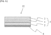
- Fig. 5 is a schematic cross-sectional view showing a wavelength conversion member according to a fifth embodiment of the present invention.
- the wavelength conversion member 15 includes a phosphor layer 1, light-transmissive heat dissipation layers 2 formed on both surfaces of the phosphor layer 1, and a reflective layer 6 formed on a surface of one of the light-transmissive heat dissipation layers 2.
- the wavelength conversion member 15 according to this embodiment is a reflective wavelength conversion member.
- the fluorescence is reflected on the reflective layer 6 and then radiated to the outside through the same light-transmissive heat dissipation layer 2 as that through which the light has entered.
- part of the excitation light having entered the wavelength conversion member 15 is converted in wavelength to fluorescence by the phosphor layer 1.
- the fluorescence is, together with part of the excitation light not converted in wavelength, reflected on the reflective layer 6 and then radiated to the outside through the same light-transmissive heat dissipation layer 2 as that through which the light has entered.
- An example of the reflective layer 6 that can be cited is a metallic layer, a dielectric multi-layer or a reflective glass layer.
- An example of the metallic layer that can be cited is a substrate or thin film made of silver, aluminum or platinum.
- Examples of a method for forming a thin metal film that can be cited include plating as well as vacuum deposition, ion plating, and sputtering which are physical vapor deposition methods.
- a thin silver film can be formed by applying a paste of silver clay on the light-transmissive heat dissipation layer 2 and applying heat to the paste.
- the dielectric multi-layer has a structure formed by alternately depositing low-refractive index layers made of silicon oxide or the like and high-refractive index layers made of niobium oxide, titanium oxide, lanthanum oxide, tantalum oxide, yttrium oxide, gadolinium oxide, tungsten oxide, hafnium oxide, aluminum oxide, silicon nitride or the like.
- Examples of a method for forming a dielectric multi-layer that can be cited include vacuum deposition, ion plating, and sputtering.
- the reflective glass layer is composed of, for example, a glass matrix and high-refraction inorganic particles dispersed in the glass matrix.
- the glass matrix that can be cited include borosilicate-based glasses.
- the inorganic particles that can be cited include at least one oxide or nitride selected from the group consisting of Al, Nb, Ti, Ta, La, Zr, Ce, Ga, Mg, Si, and Zn.
- the reflective glass layer can be produced in the following manner.
- a green sheet for a reflective glass layer is produced by applying a slurry containing glass powder to be a glass matrix, inorganic particles, and organic components such as a binder resin and a solvent to a resin film made of polyethylene terephthalate or other materials by the doctor blade method or other methods and then drying the slurry by the application of heat. The green sheet is fired, thus obtaining a reflective glass layer.
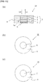
- Fig. 6(a) is a schematic cross-sectional view showing a wavelength conversion member according to a sixth embodiment of the present invention.
- Fig. 6(b) is a schematic plan view of the wavelength conversion member 16 of Fig. 6 (a) when viewed from the opposite side to an incident surface thereof through which excitation light L0 enters the wavelength conversion member 16
- Fig. 6(c) is a schematic plan view of the wavelength conversion member 16 of Fig. 6 (a) when viewed from the incident surface thereof through which excitation light L0 enters the wavelength conversion member 16.
- the wavelength conversion member 16 is different from the wavelength conversion member 15 according to the fifth embodiment in that a heat dissipating member 4 is provided to surround the lateral periphery of a laminate 3 formed of a phosphor layer 1 and light-transmissive heat dissipation layers 2.
- the laminate 3 is bonded tightly to the inside of a hole 4a provided substantially in the center of the heat dissipating member 4. Heat generated in the phosphor layer 1 is released through the light-transmissive heat dissipation layer 2 to the outside or directly transferred to the heat dissipating member 4 and then released from the heat dissipating member 4 to the outside.
- the laminate 3 has a columnar shape, it may have a prismatic shape, such as a triangular prism or a quadratic prism. Furthermore, a reflective layer (not shown) may be provided at the interface between the laminate 3 and the heat dissipating member 4.
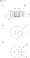
- Fig. 7(a) is a schematic cross-sectional view showing a wavelength conversion member according to a seventh embodiment of the present invention.
- Fig. 7(b) is a schematic plan view of the wavelength conversion member 17 of Fig. 7(a) when viewed from the opposite side to an incident surface thereof through which excitation light L0 enters the wavelength conversion member 17
- Fig. 7(c) is a schematic plan view of the wavelength conversion member 17 of Fig. 7(a) when viewed from the incident surface thereof through which excitation light L0 enters the wavelength conversion member 17.
- the wavelength conversion member 17 according to this embodiment is different from the wavelength conversion member 16 according to the sixth embodiment in that a scattering layer 5 is provided on an incident surface of a laminate 3 through which excitation light L0 enters the wavelength conversion member 17, the laminate 3 being formed of a phosphor layer 1 and light-transmissive heat dissipation layers 2.
- the excitation light L0 is first scattered in the scattering layer 5 and then applied to the phosphor layer 1, which makes it possible to reduce the energy density of the excitation light L0 applied to the phosphor layer 1.
- excessive temperature rise of the phosphor layer 1 can be reduced.
- Fig. 8 is a schematic side view of a light emitting device in which the wavelength conversion member according to the first embodiment of the present invention is used.
- the light emitting device according to this embodiment is a light emitting device in which a transmissive wavelength conversion member is used.
- the light emitting device 21 includes a wavelength conversion member 11 and a light source 7. Excitation light L0 emitted from the light source 7 is converted in wavelength to fluorescence L1 having a longer wavelength than the excitation light L0 by the phosphor layer 1 in the wavelength conversion member 11. Furthermore, part of the excitation light L0 passes through the wavelength conversion member 11. Therefore, the wavelength conversion member 11 emits synthetic light L2 composed of the excitation light L0 and the fluorescence L1. For example, when the excitation light L0 is a blue light and the fluorescence L1 is a yellow light, a white synthetic light L2 can be provided.
- the wavelength conversion member 11 is formed of a laminate 3 that includes: a phosphor layer 1; and light-transmissive heat dissipation layers 2 formed on both surfaces of the phosphor layer 1. Therefore, heat generated by the irradiation of the phosphor layer 1 with the excitation light L0 is released through the light-transmissive heat dissipation layers 2 to the outside. Thus, an undue temperature rise of the phosphor layer 1 can be reduced.
- Examples of the light source 7 that can be cited include an LED and an LD. From the viewpoint of increasing the luminescence intensity of the light emitting device 21, an LD capable of emitting high-intensity light is preferably used as the light source 7.
- any one of the wavelength conversion members 12 to 15 according to the second to fifth embodiments may be used.
- Fig. 9 is a schematic side view of a light emitting device in which the wavelength conversion member according to the fifth embodiment of the present invention is used.
- the light emitting device according to this embodiment is a light emitting device in which a reflective wavelength conversion member is used.
- the light emitting device 22 includes a wavelength conversion member 15, a light source 7, and a beam splitter 8.
- Light L0 emitted from the light source 7 is guided to the wavelength conversion member 15 by the beam splitter 8 and then converted in wavelength to light L1 having a longer wavelength than the light L0 by the phosphor layer 1 in the wavelength conversion member 15.
- the light L1 is reflected toward the incident surface side by the reflective layer 6, passes through the beam splitter 8, and is then emitted to the outside.
- light-transmissive heat dissipation layers 2 are formed on both surfaces of the phosphor layer 1 in the wavelength conversion member 15. Therefore, heat generated by the irradiation of the phosphor layer 1 with the excitation light L0 is released through the light-transmissive heat dissipation layers 2 to the outside. Thus, an undue temperature rise of the phosphor layer 1 can be reduced.
- the wavelength conversion member of the present invention is suitable as a component of a general lighting, such as a white LED, or a special lighting (for example, a light source for a projector, a light source for a vehicle headlight or a light source for an endoscope).
- a general lighting such as a white LED
- a special lighting for example, a light source for a projector, a light source for a vehicle headlight or a light source for an endoscope.
Landscapes
- Engineering & Computer Science (AREA)
- Physics & Mathematics (AREA)
- Chemical & Material Sciences (AREA)
- Microelectronics & Electronic Packaging (AREA)
- Spectroscopy & Molecular Physics (AREA)
- General Engineering & Computer Science (AREA)
- Computer Hardware Design (AREA)
- Manufacturing & Machinery (AREA)
- Power Engineering (AREA)
- Organic Chemistry (AREA)
- Materials Engineering (AREA)
- Optics & Photonics (AREA)
- Chemical Kinetics & Catalysis (AREA)
- Thermal Sciences (AREA)
- Combustion & Propulsion (AREA)
- General Physics & Mathematics (AREA)
- Electromagnetism (AREA)
- Condensed Matter Physics & Semiconductors (AREA)
- Inorganic Chemistry (AREA)
- Led Device Packages (AREA)
- Optical Filters (AREA)
- Semiconductor Lasers (AREA)
- Non-Portable Lighting Devices Or Systems Thereof (AREA)
- Compositions Of Oxide Ceramics (AREA)
Applications Claiming Priority (4)
| Application Number | Priority Date | Filing Date | Title |
|---|---|---|---|
| JP2014104995 | 2014-05-21 | ||
| JP2014129818 | 2014-06-25 | ||
| JP2015061937A JP2016027613A (ja) | 2014-05-21 | 2015-03-25 | 波長変換部材及びそれを用いた発光装置 |
| PCT/JP2015/063290 WO2015178223A1 (fr) | 2014-05-21 | 2015-05-08 | Organe de conversion de longueur d'onde et dispositif électroluminescent l'utilisant |
Publications (2)
| Publication Number | Publication Date |
|---|---|
| EP3147955A1 true EP3147955A1 (fr) | 2017-03-29 |
| EP3147955A4 EP3147955A4 (fr) | 2018-01-24 |
Family
ID=54553896
Family Applications (1)
| Application Number | Title | Priority Date | Filing Date |
|---|---|---|---|
| EP15796573.2A Withdrawn EP3147955A4 (fr) | 2014-05-21 | 2015-05-08 | Organe de conversion de longueur d'onde et dispositif électroluminescent l'utilisant |
Country Status (6)
| Country | Link |
|---|---|
| US (1) | US10047285B2 (fr) |
| EP (1) | EP3147955A4 (fr) |
| JP (1) | JP2016027613A (fr) |
| CN (1) | CN106030835A (fr) |
| TW (1) | TW201608005A (fr) |
| WO (1) | WO2015178223A1 (fr) |
Cited By (5)
| Publication number | Priority date | Publication date | Assignee | Title |
|---|---|---|---|---|
| GB2548706A (en) * | 2016-02-24 | 2017-09-27 | Nichia Corp | Method of manufacturing fluorescent-material-containing member |
| EP3236136A1 (fr) * | 2016-04-20 | 2017-10-25 | Panasonic Intellectual Property Management Co., Ltd. | Élément de conversion de longueur d'onde comprenant un luminophore convertissant la lumière d'un élément électroluminescent à semi-conducteur en lumière de longueur d'onde plus longue |
| WO2020030525A1 (fr) * | 2018-08-10 | 2020-02-13 | Osram Opto Semiconductors Gmbh | Convertisseur pour un composant optoélectronique, composant optoélectronique, procédé de formation d'un convertisseur pour un composant optoélectronique et matériau pour un réflecteur d'un composant optoélectronique |
| EP4036624A4 (fr) * | 2019-09-27 | 2023-05-10 | Sony Group Corporation | Dispositif électroluminescent, unité de conversion de longueur d'onde, et phare ou dispositif d'affichage |
| EP4258369A1 (fr) * | 2022-03-31 | 2023-10-11 | Nichia Corporation | Élément optique et dispositif électroluminescent |
Families Citing this family (59)
| Publication number | Priority date | Publication date | Assignee | Title |
|---|---|---|---|---|
| JP6604543B2 (ja) * | 2013-08-09 | 2019-11-13 | 株式会社タムラ製作所 | 発光装置 |
| KR20160028580A (ko) * | 2014-09-03 | 2016-03-14 | 삼성디스플레이 주식회사 | 컬러 변환층을 포함하는 표시장치 |
| JP6597964B2 (ja) * | 2015-12-10 | 2019-10-30 | 日本電気硝子株式会社 | 波長変換部材及び波長変換素子、並びにそれを用いた発光装置 |
| JP2017107071A (ja) * | 2015-12-10 | 2017-06-15 | 日本電気硝子株式会社 | 波長変換部材及び波長変換素子、並びにそれらを用いた発光装置 |
| JP2017111176A (ja) * | 2015-12-14 | 2017-06-22 | セイコーエプソン株式会社 | 波長変換素子、照明装置、プロジェクター、および波長変換素子の製造方法 |
| US10707385B2 (en) * | 2016-01-22 | 2020-07-07 | Ngk Spark Plug Co., Ltd. | Wavelength conversion member and light-emitting device |
| JP6469893B2 (ja) * | 2016-01-26 | 2019-02-13 | シャープ株式会社 | 発光装置および照明装置 |
| JP2017167309A (ja) * | 2016-03-16 | 2017-09-21 | キヤノン株式会社 | 光学素子、光源装置および画像投射装置 |
| EP3432370B1 (fr) | 2016-03-18 | 2021-08-04 | Koito Manufacturing Co., Ltd. | Élément fluorescent et module électroluminescent |
| CN108780169B (zh) * | 2016-03-25 | 2020-06-05 | 东丽株式会社 | 光源单元、层叠构件及使用它们的显示器及照明装置 |
| JP6852976B2 (ja) * | 2016-03-29 | 2021-03-31 | 日本特殊陶業株式会社 | 波長変換部材、その製造方法および発光装置 |
| WO2017195303A1 (fr) * | 2016-05-11 | 2017-11-16 | オリンパス株式会社 | Dispositif d'éclairage |
| JP6493308B2 (ja) | 2016-05-31 | 2019-04-03 | 日亜化学工業株式会社 | 発光装置 |
| JP6935990B2 (ja) * | 2016-06-16 | 2021-09-15 | 株式会社小糸製作所 | 波長変換部材、発光装置および波長変換部材の製造方法 |
| DE102016113470A1 (de) * | 2016-07-21 | 2018-01-25 | Osram Opto Semiconductors Gmbh | Laserbauelement |
| KR101869230B1 (ko) * | 2016-07-28 | 2018-07-19 | 주식회사 제이케이리서치 | 파장선택성 나노다공 구조체 |
| JP6648660B2 (ja) | 2016-09-21 | 2020-02-14 | 日亜化学工業株式会社 | 蛍光体含有部材及び蛍光体含有部材を備える発光装置 |
| JPWO2018074132A1 (ja) * | 2016-10-21 | 2019-08-15 | 日本電気硝子株式会社 | 波長変換部材、発光デバイス及び波長変換部材の製造方法 |
| CN106949393A (zh) * | 2016-12-21 | 2017-07-14 | 刘锋 | 一种可以透光,滤光的散热装置及led灯具 |
| JP6834478B2 (ja) * | 2016-12-28 | 2021-02-24 | ウシオ電機株式会社 | 蛍光光源装置およびその製造方法 |
| CN106876551A (zh) * | 2016-12-30 | 2017-06-20 | 东莞中之光电股份有限公司 | 芯片级led封装工艺 |
| CN106876528A (zh) * | 2016-12-30 | 2017-06-20 | 东莞中之光电股份有限公司 | Led封装制作工艺 |
| JP6631553B2 (ja) | 2017-02-09 | 2020-01-15 | 日亜化学工業株式会社 | 発光装置の製造方法 |
| JP6544408B2 (ja) * | 2017-03-03 | 2019-07-17 | 日亜化学工業株式会社 | 光学部品及び光学部品の製造方法 |
| JP2018151610A (ja) * | 2017-03-10 | 2018-09-27 | 日本電気硝子株式会社 | 波長変換部材及び発光デバイス |
| WO2018163691A1 (fr) * | 2017-03-10 | 2018-09-13 | 日本電気硝子株式会社 | Élément de conversion de longueur d'onde et dispositif électroluminescent |
| JP6848582B2 (ja) * | 2017-03-24 | 2021-03-24 | 日本電気硝子株式会社 | 波長変換部材及び発光デバイス |
| KR101917703B1 (ko) | 2017-04-04 | 2019-01-29 | 엘지전자 주식회사 | 형광체 모듈 |
| WO2018219346A1 (fr) * | 2017-06-01 | 2018-12-06 | 苏州欧普照明有限公司 | Procédé de chauffage a del, dispositif, composant, dispositif de chauffage de salle de bains et dispositif de réchauffement |
| DE102017210512A1 (de) * | 2017-06-22 | 2018-12-27 | Osram Gmbh | Konverter, laser activated remote phosphor (larp) system und scheinwerfer |
| CN109143745B (zh) * | 2017-06-27 | 2021-02-26 | 深圳光峰科技股份有限公司 | 发光聚集器、发光设备及投影光源 |
| JP7016037B2 (ja) * | 2017-06-30 | 2022-02-04 | パナソニックIpマネジメント株式会社 | 発光体及び発光装置 |
| CN109424944A (zh) * | 2017-07-13 | 2019-03-05 | 深圳光峰科技股份有限公司 | 一种波长转换装置及光源 |
| CN109424942A (zh) * | 2017-07-21 | 2019-03-05 | 深圳光峰科技股份有限公司 | 波长转换装置、包含其的光源及投影装置 |
| JP7120745B2 (ja) * | 2017-09-29 | 2022-08-17 | 日本特殊陶業株式会社 | 光波長変換装置及び光複合装置 |
| WO2019107918A1 (fr) * | 2017-11-28 | 2019-06-06 | 주식회사 베이스 | Procédé de production d'un élément de conversion de couleurs de luminophores phosphorescents inclus dans du verre |
| CN108303822A (zh) * | 2018-01-23 | 2018-07-20 | 青岛海信电器股份有限公司 | 一种背光模组、显示装置及液晶电视 |
| CN111699419B (zh) * | 2018-02-19 | 2022-09-09 | 日本碍子株式会社 | 光学部件及照明装置 |
| WO2019203520A1 (fr) * | 2018-04-17 | 2019-10-24 | 엘지전자 주식회사 | Module de phosphore |
| US10921697B2 (en) * | 2018-04-26 | 2021-02-16 | Panasonic Intellectual Property Management Co., Ltd. | Wavelength conversion element, phosphor wheel, light source device, and projection display apparatus |
| CN110579932B (zh) | 2018-06-11 | 2023-12-05 | 中强光电股份有限公司 | 波长转换元件、投影装置及波长转换元件的制作方法 |
| CN110579933B (zh) * | 2018-06-11 | 2022-06-14 | 中强光电股份有限公司 | 波长转换元件、投影装置及波长转换元件的制作方法 |
| JP6943984B2 (ja) * | 2018-06-18 | 2021-10-06 | 日本特殊陶業株式会社 | 光波長変換装置及び発光装置 |
| WO2020002074A1 (fr) | 2018-06-26 | 2020-01-02 | Lumileds Holding B.V. | Dispositif de conversion de lumière à couche de protection en céramique |
| US11131433B2 (en) | 2018-08-20 | 2021-09-28 | Nichia Corporation | Fluorescent module and illumination device |
| CN110873319A (zh) * | 2018-09-03 | 2020-03-10 | 深圳光峰科技股份有限公司 | 波长转换装置及光源系统 |
| CN110887022A (zh) * | 2018-09-10 | 2020-03-17 | 深圳光峰科技股份有限公司 | 波长转换装置及光源系统 |
| JP6879290B2 (ja) * | 2018-12-26 | 2021-06-02 | 日亜化学工業株式会社 | 発光装置 |
| CN110253986B (zh) * | 2019-02-28 | 2021-08-24 | 罗化芯显示科技开发(江苏)有限公司 | 荧光陶瓷及其制备方法 |
| WO2020189405A1 (fr) * | 2019-03-19 | 2020-09-24 | シャープ株式会社 | Élément optique, phare avant de véhicule, dispositif source de lumière et dispositif de projection |
| CN111812928A (zh) | 2019-04-12 | 2020-10-23 | 中强光电股份有限公司 | 波长转换装置与投影装置 |
| JP6954329B2 (ja) | 2019-06-25 | 2021-10-27 | セイコーエプソン株式会社 | 波長変換素子、光源装置およびプロジェクター |
| TWI739506B (zh) * | 2019-07-16 | 2021-09-11 | 日商日本特殊陶業股份有限公司 | 焊接用波長轉換構件、波長轉換裝置及光源裝置 |
| WO2021132212A1 (fr) * | 2019-12-23 | 2021-07-01 | 日本電気硝子株式会社 | Élément de conversion de longueur d'onde, élément électroluminescent et dispositif électroluminescent |
| JP7472558B2 (ja) | 2020-03-12 | 2024-04-23 | セイコーエプソン株式会社 | 波長変換素子、光源装置、プロジェクター、および波長変換素子の製造方法 |
| KR20220156545A (ko) * | 2020-03-19 | 2022-11-25 | 닛토덴코 가부시키가이샤 | 광전기 전송 복합 모듈 |
| JP2022149549A (ja) | 2021-03-25 | 2022-10-07 | セイコーエプソン株式会社 | 波長変換装置、光源装置及びプロジェクター |
| CN114335293B (zh) * | 2021-12-28 | 2024-03-19 | 广东省科学院半导体研究所 | 一种量子点光转换模组、微led显示器及其制备方法 |
| CN114736006B (zh) * | 2022-04-06 | 2023-02-28 | 南京邮电大学 | 一种具有梳状导热结构的复合荧光陶瓷及其制备方法 |
Family Cites Families (12)
| Publication number | Priority date | Publication date | Assignee | Title |
|---|---|---|---|---|
| TW383508B (en) | 1996-07-29 | 2000-03-01 | Nichia Kagaku Kogyo Kk | Light emitting device and display |
| JP4158012B2 (ja) | 2002-03-06 | 2008-10-01 | 日本電気硝子株式会社 | 発光色変換部材 |
| KR101370362B1 (ko) * | 2005-03-14 | 2014-03-05 | 코닌클리케 필립스 엔.브이. | 다결정 세라믹 구조 내의 인광체 및 이를 포함하는 발광 요소 |
| CN100566490C (zh) * | 2005-03-14 | 2009-12-02 | 皇家飞利浦电子股份有限公司 | 多晶陶瓷结构中的磷光体和包括该磷光体的发光元件 |
| JP4895541B2 (ja) | 2005-07-08 | 2012-03-14 | シャープ株式会社 | 波長変換部材、発光装置及び波長変換部材の製造方法 |
| JP2007048864A (ja) * | 2005-08-09 | 2007-02-22 | Nippon Electric Glass Co Ltd | 蛍光体複合材料 |
| JP2008169348A (ja) * | 2007-01-15 | 2008-07-24 | Nippon Electric Glass Co Ltd | 蛍光体複合材料 |
| CN105481362A (zh) | 2008-06-02 | 2016-04-13 | 松下电器产业株式会社 | 半导体发光设备以及使用所述半导体发光设备的光源设备 |
| JP2011071404A (ja) * | 2009-09-28 | 2011-04-07 | Kyocera Corp | 発光装置および照明装置 |
| TWI486254B (zh) * | 2010-09-20 | 2015-06-01 | Nitto Denko Corp | 發光陶瓷層板及其製造方法 |
| US8846172B2 (en) * | 2010-10-18 | 2014-09-30 | Nitto Denko Corporation | Light emissive ceramic laminate and method of making same |
| JP5549539B2 (ja) * | 2010-10-28 | 2014-07-16 | 日本電気硝子株式会社 | 波長変換素子、それを備える光源及びその製造方法 |
-
2015
- 2015-03-25 JP JP2015061937A patent/JP2016027613A/ja active Pending
- 2015-05-08 WO PCT/JP2015/063290 patent/WO2015178223A1/fr active Application Filing
- 2015-05-08 EP EP15796573.2A patent/EP3147955A4/fr not_active Withdrawn
- 2015-05-08 US US15/311,535 patent/US10047285B2/en active Active
- 2015-05-08 CN CN201580009421.3A patent/CN106030835A/zh active Pending
- 2015-05-19 TW TW104115941A patent/TW201608005A/zh unknown
Cited By (9)
| Publication number | Priority date | Publication date | Assignee | Title |
|---|---|---|---|---|
| GB2548706A (en) * | 2016-02-24 | 2017-09-27 | Nichia Corp | Method of manufacturing fluorescent-material-containing member |
| US10400993B2 (en) | 2016-02-24 | 2019-09-03 | Nichia Corporation | Method of manufacturing fluorescent-material-containing member |
| GB2548706B (en) * | 2016-02-24 | 2019-12-11 | Nichia Corp | Method of manufacturing fluorescent-material-containing member |
| EP3236136A1 (fr) * | 2016-04-20 | 2017-10-25 | Panasonic Intellectual Property Management Co., Ltd. | Élément de conversion de longueur d'onde comprenant un luminophore convertissant la lumière d'un élément électroluminescent à semi-conducteur en lumière de longueur d'onde plus longue |
| US10094529B2 (en) | 2016-04-20 | 2018-10-09 | Panasonic Intellectual Property Management Co., Ltd. | Wavelength conversion member including phosphor that converts light from semiconductor light-emitting element into longer-wavelength light |
| WO2020030525A1 (fr) * | 2018-08-10 | 2020-02-13 | Osram Opto Semiconductors Gmbh | Convertisseur pour un composant optoélectronique, composant optoélectronique, procédé de formation d'un convertisseur pour un composant optoélectronique et matériau pour un réflecteur d'un composant optoélectronique |
| US10622524B2 (en) | 2018-08-10 | 2020-04-14 | Osram Opto Semiconductors Gmbh | Converter for an optoelectronic component, optoelectronic component, method for forming a converter for an optoelectronic component and material for a reflector of an optoelectronic component |
| EP4036624A4 (fr) * | 2019-09-27 | 2023-05-10 | Sony Group Corporation | Dispositif électroluminescent, unité de conversion de longueur d'onde, et phare ou dispositif d'affichage |
| EP4258369A1 (fr) * | 2022-03-31 | 2023-10-11 | Nichia Corporation | Élément optique et dispositif électroluminescent |
Also Published As
| Publication number | Publication date |
|---|---|
| EP3147955A4 (fr) | 2018-01-24 |
| WO2015178223A1 (fr) | 2015-11-26 |
| CN106030835A (zh) | 2016-10-12 |
| US10047285B2 (en) | 2018-08-14 |
| TW201608005A (zh) | 2016-03-01 |
| US20170137706A1 (en) | 2017-05-18 |
| JP2016027613A (ja) | 2016-02-18 |
Similar Documents
| Publication | Publication Date | Title |
|---|---|---|
| US10047285B2 (en) | Wavelength conversion member and light emitting device using same | |
| JP5966501B2 (ja) | 波長変換用無機成形体及びその製造方法、並びに発光装置 | |
| JP5678885B2 (ja) | 波長変換素子、光源及び液晶用バックライトユニット | |
| US10267963B2 (en) | Wavelength conversion member, wavelength conversion element, and light emitting apparatus using those | |
| JP6069890B2 (ja) | 波長変換用無機成形体及び発光装置 | |
| EP3637482B1 (fr) | Élément convertisseur de longueur d'onde et source de lumière le comprenant | |
| JP5966539B2 (ja) | 波長変換用無機成形体及びその製造方法、並びに発光装置 | |
| TW201531789A (zh) | 投影機用螢光輪、其製造方法及投影機用發光裝置 | |
| KR20130110101A (ko) | 파장 변환용 무기 성형체 및 그 제조 방법, 및 발광 장치 | |
| CN105481362A (zh) | 半导体发光设备以及使用所述半导体发光设备的光源设备 | |
| JP2016225581A (ja) | 波長変換部材及びそれを用いた発光装置 | |
| TW201920608A (zh) | 光波長轉換裝置及光複合裝置 | |
| JP6943984B2 (ja) | 光波長変換装置及び発光装置 | |
| JP5966529B2 (ja) | 波長変換用無機成形体及び発光装置 | |
| JP2017085038A (ja) | 波長変換素子の製造方法 | |
| JP5585421B2 (ja) | 波長変換素子及びそれを備える光源 | |
| JP2016018921A (ja) | 波長変換部材及び発光デバイス | |
| JP2012094741A (ja) | 波長変換素子及びそれを備える光源 | |
| US20190378958A1 (en) | Optoelectronic component and method of manufacturing an optoelectronic component | |
| US11635189B2 (en) | Phosphor element and lighting device | |
| JP6848582B2 (ja) | 波長変換部材及び発光デバイス | |
| JP2017085039A (ja) | 波長変換素子の製造方法並びに波長変換素子及び発光装置 |
Legal Events
| Date | Code | Title | Description |
|---|---|---|---|
| PUAI | Public reference made under article 153(3) epc to a published international application that has entered the european phase |
Free format text: ORIGINAL CODE: 0009012 |
|
| 17P | Request for examination filed |
Effective date: 20161109 |
|
| AK | Designated contracting states |
Kind code of ref document: A1 Designated state(s): AL AT BE BG CH CY CZ DE DK EE ES FI FR GB GR HR HU IE IS IT LI LT LU LV MC MK MT NL NO PL PT RO RS SE SI SK SM TR |
|
| AX | Request for extension of the european patent |
Extension state: BA ME |
|
| DAV | Request for validation of the european patent (deleted) | ||
| DAX | Request for extension of the european patent (deleted) | ||
| A4 | Supplementary search report drawn up and despatched |
Effective date: 20171221 |
|
| RIC1 | Information provided on ipc code assigned before grant |
Ipc: F21Y 115/30 20160101ALI20171215BHEP Ipc: F21V 9/16 00000000ALI20171215BHEP Ipc: H01L 33/60 20100101ALI20171215BHEP Ipc: F21K 9/64 20160101ALI20171215BHEP Ipc: C09K 5/14 20060101ALI20171215BHEP Ipc: H01S 5/02 20060101ALI20171215BHEP Ipc: H01L 33/64 20100101ALI20171215BHEP Ipc: H01L 33/50 20100101AFI20171215BHEP Ipc: H05B 33/22 20060101ALI20171215BHEP |
|
| RIC1 | Information provided on ipc code assigned before grant |
Ipc: F21V 9/16 20060101ALI20171215BHEP Ipc: F21Y 115/30 20160101ALI20171215BHEP Ipc: H01L 33/64 20100101ALI20171215BHEP Ipc: H01L 33/50 20100101AFI20171215BHEP Ipc: H01S 5/02 20060101ALI20171215BHEP Ipc: F21K 9/64 20160101ALI20171215BHEP Ipc: H05B 33/22 20060101ALI20171215BHEP Ipc: H01L 33/60 20100101ALI20171215BHEP Ipc: C09K 5/14 20060101ALI20171215BHEP |
|
| 17Q | First examination report despatched |
Effective date: 20200108 |
|
| STAA | Information on the status of an ep patent application or granted ep patent |
Free format text: STATUS: THE APPLICATION HAS BEEN WITHDRAWN |
|
| 18W | Application withdrawn |
Effective date: 20200327 |