EP3128555B1 - Leuchtdiodenchip mit integriertem schutz gegen elektrostatische entladungen und entsprechendes herstellungsverfahren - Google Patents
Leuchtdiodenchip mit integriertem schutz gegen elektrostatische entladungen und entsprechendes herstellungsverfahren Download PDFInfo
- Publication number
- EP3128555B1 EP3128555B1 EP16187828.5A EP16187828A EP3128555B1 EP 3128555 B1 EP3128555 B1 EP 3128555B1 EP 16187828 A EP16187828 A EP 16187828A EP 3128555 B1 EP3128555 B1 EP 3128555B1
- Authority
- EP
- European Patent Office
- Prior art keywords
- layer
- semiconductor
- semiconductor layer
- radiation
- semiconductor chip
- Prior art date
- Legal status (The legal status is an assumption and is not a legal conclusion. Google has not performed a legal analysis and makes no representation as to the accuracy of the status listed.)
- Active
Links
Images


Classifications
-
- H—ELECTRICITY
- H10—SEMICONDUCTOR DEVICES; ELECTRIC SOLID-STATE DEVICES NOT OTHERWISE PROVIDED FOR
- H10H—INORGANIC LIGHT-EMITTING SEMICONDUCTOR DEVICES HAVING POTENTIAL BARRIERS
- H10H29/00—Integrated devices, or assemblies of multiple devices, comprising at least one light-emitting semiconductor element covered by group H10H20/00
- H10H29/10—Integrated devices comprising at least one light-emitting semiconductor component covered by group H10H20/00
-
- H—ELECTRICITY
- H10—SEMICONDUCTOR DEVICES; ELECTRIC SOLID-STATE DEVICES NOT OTHERWISE PROVIDED FOR
- H10D—INORGANIC ELECTRIC SEMICONDUCTOR DEVICES
- H10D89/00—Aspects of integrated devices not covered by groups H10D84/00 - H10D88/00
- H10D89/60—Integrated devices comprising arrangements for electrical or thermal protection, e.g. protection circuits against electrostatic discharge [ESD]
- H10D89/601—Integrated devices comprising arrangements for electrical or thermal protection, e.g. protection circuits against electrostatic discharge [ESD] for devices having insulated gate electrodes, e.g. for IGFETs or IGBTs
- H10D89/611—Integrated devices comprising arrangements for electrical or thermal protection, e.g. protection circuits against electrostatic discharge [ESD] for devices having insulated gate electrodes, e.g. for IGFETs or IGBTs using diodes as protective elements
-
- H—ELECTRICITY
- H10—SEMICONDUCTOR DEVICES; ELECTRIC SOLID-STATE DEVICES NOT OTHERWISE PROVIDED FOR
- H10H—INORGANIC LIGHT-EMITTING SEMICONDUCTOR DEVICES HAVING POTENTIAL BARRIERS
- H10H20/00—Individual inorganic light-emitting semiconductor devices having potential barriers, e.g. light-emitting diodes [LED]
- H10H20/80—Constructional details
- H10H20/81—Bodies
-
- H—ELECTRICITY
- H10—SEMICONDUCTOR DEVICES; ELECTRIC SOLID-STATE DEVICES NOT OTHERWISE PROVIDED FOR
- H10H—INORGANIC LIGHT-EMITTING SEMICONDUCTOR DEVICES HAVING POTENTIAL BARRIERS
- H10H20/00—Individual inorganic light-emitting semiconductor devices having potential barriers, e.g. light-emitting diodes [LED]
- H10H20/80—Constructional details
- H10H20/83—Electrodes
- H10H20/831—Electrodes characterised by their shape
- H10H20/8312—Electrodes characterised by their shape extending at least partially through the bodies
-
- H—ELECTRICITY
- H10—SEMICONDUCTOR DEVICES; ELECTRIC SOLID-STATE DEVICES NOT OTHERWISE PROVIDED FOR
- H10H—INORGANIC LIGHT-EMITTING SEMICONDUCTOR DEVICES HAVING POTENTIAL BARRIERS
- H10H20/00—Individual inorganic light-emitting semiconductor devices having potential barriers, e.g. light-emitting diodes [LED]
- H10H20/80—Constructional details
- H10H20/85—Packages
- H10H20/857—Interconnections, e.g. lead-frames, bond wires or solder balls
-
- H—ELECTRICITY
- H01—ELECTRIC ELEMENTS
- H01L—SEMICONDUCTOR DEVICES NOT COVERED BY CLASS H10
- H01L2924/00—Indexing scheme for arrangements or methods for connecting or disconnecting semiconductor or solid-state bodies as covered by H01L24/00
- H01L2924/0001—Technical content checked by a classifier
- H01L2924/0002—Not covered by any one of groups H01L24/00, H01L24/00 and H01L2224/00
Definitions
- the present application relates to a radiation-emitting semiconductor chip and a method for producing a radiation-emitting semiconductor chip.
- a radiation-emitting semiconductor chip has a carrier and a semiconductor body with a semiconductor layer sequence.
- the semiconductor layer sequence has an active region provided for generating radiation, a first semiconductor layer and a second semiconductor layer.
- the active area is arranged between the first semiconductor layer and the second semiconductor layer.
- the first semiconductor layer is arranged on the side of the active region facing away from the carrier.
- the semiconductor body has at least one recess which extends through the active region.
- the first semiconductor layer is connected in an electrically conductive manner to a first connection layer, the first connection layer extending in the recess from the first semiconductor layer in the direction of the carrier.
- the first connection layer is electrically connected to the second semiconductor layer via a protective diode.
- the protective diode is integrated into the semiconductor chip.
- the risk of damage to the semiconductor chip, for example due to electrostatic discharge, is thus reduced.
- An additional protective diode to be arranged outside the semiconductor chip and connected to it in an electrically conductive manner can be dispensed with.
- the protective diode can in particular fulfill the function of an ESD (Electrostatic Discharge) diode which protects the semiconductor chip from damage by electrostatic discharge.
- ESD Electrostatic Discharge
- charge carriers can flow away via a current path between the first connection layer and the second semiconductor layer. The risk of damage to the semiconductor chip can thus be reduced.
- the first semiconductor layer and the second semiconductor layer of the semiconductor body are expediently different from one another with regard to their conductivity type.
- the first semiconductor layer can be p-conductive and the second semiconductor layer n-conductive, or vice versa.
- a diode structure in which the active area is formed is thus implemented in a simple manner.
- the protective diode is formed between the first connection layer and the second semiconductor layer.
- the protective diode can thus be arranged in a simple manner in a current path between the first connection layer and the second semiconductor layer.
- the protective diode can be formed outside the carrier.
- the protective diode can thus be formed largely independently of the properties of the carrier, in particular the electrical conductivity or the electrical contactability.
- the semiconductor chip furthermore preferably has a first contact and a second contact, which are each provided for the external electrical contacting of the semiconductor chip.
- An operating voltage applied between the first contact and the second contact causes charge carriers to be injected into the active area from different sides of the active area.
- the injected charge carriers can recombine with the emission of radiation in the active area.
- the diode structure of the semiconductor body and the protective diode are expediently formed antiparallel to one another.
- the protective diode is designed as a Schottky diode.
- a Schottky diode can in particular be formed by means of a metal-semiconductor junction, the current-voltage characteristic of the junction deviating from an ohmic characteristic and, in particular, running asymmetrically with respect to the polarity of the applied voltage.
- the protective diode overlaps with the semiconductor body in a plan view of the semiconductor chip.
- the semiconductor body in particular the active area, can completely cover the protective diode in plan view.
- the protective diode can thus be integrated into the semiconductor chip with the same lateral extent of the semiconductor body. Furthermore, the protective diode can thus be integrated into the semiconductor chip while maintaining the area of the active region that can be used for generating radiation.
- a lateral direction is understood to mean a direction which runs along a main plane of extent of the semiconductor layers of the semiconductor body.
- the protective diode is formed by means of the second semiconductor layer.
- the second semiconductor layer can therefore be provided both for the injection of charge carriers into the active region and for the formation of the protective diode.
- a separate semiconductor region, which is electrically isolated from the active region, for forming the Schottky diode can thus be dispensed with.
- the protective diode in particular in the form of a Schottky diode, can be integrated into the semiconductor chip with the same lateral extent of the semiconductor chip, without reducing the area of the active region that is decisive for generating radiation.
- the protection diode can thus be integrated into the semiconductor chip without impairing the optoelectronic properties of the semiconductor chip.
- the first connection layer runs at least in some areas between the carrier and the second semiconductor layer.
- electrical contact can be made with the first semiconductor layer from the side of the active region facing the carrier.
- a second connection layer is arranged at least in regions between the first connection layer and the second semiconductor layer.
- the second connection layer is connected in an electrically conductive manner to the second semiconductor layer and furthermore preferably directly adjoins the second semiconductor layer.
- the first connection layer and the second connection layer can each be electrically contacted externally via the first and second contact, respectively.
- the first and / or the second contact can each be formed by means of a contact layer which is arranged, preferably directly, on the first or second connection layer.
- the first connection layer can form the first contact and / or the second connection layer can form the second contact.
- at least one separate contact layer which is provided in addition to the connection layers and forms the first or second contact, can be dispensed with.
- the first connection layer and / or the second connection layer preferably each contain a metal, for example Ti, Pt, Ni, Au, Ag, Al, Rh, Pd, Pt or W or a metallic alloy with at least one of the materials mentioned.
- the first and / or the second connection layer are preferably arranged outside the semiconductor body and fabricated by a non-epitaxial process such as vapor deposition or sputtering.
- the protective diode is formed by means of a transition layer which is arranged on the second semiconductor layer and furthermore preferably adjoins the second semiconductor layer.
- the transition layer and the second connection layer are expediently spaced apart from one another in the lateral direction. A direct electrical contact between the transition layer and the second connection layer can thus be avoided in a simple manner.
- an insulation layer is preferably formed between the transition layer and the second connection layer. The risk of an electrical short circuit between the transition layer and the second connection layer can thus be further reduced.
- the transition layer is preferably selected in such a way that a Schottky transition, that is to say a metal-semiconductor transition with asymmetrical current-voltage characteristics, to the second semiconductor layer can be implemented in a simplified manner.
- the protective diode is formed by means of the first connection layer, the first connection layer preferably adjoining the second semiconductor layer.
- the first connection layer adjoins the first semiconductor layer and the second semiconductor layer, with an ohmic or at least approximately ohmic contact between the first connection layer and the first contact layer and between a Schottky contact is formed between the first connection layer and the second contact layer.
- the material for the layer adjoining the second semiconductor layer is preferably selected such that a Schottky contact to the second semiconductor layer can be formed in a simplified manner.
- the second semiconductor layer has, at least in some areas, in particular in the area of the protective diode, a locally targeted reduced contact capability.
- a locally targeted reduced contact capability can be produced, for example, by ashing, for example in an oxygen-containing plasma, or by sputtering. In this way, the electrical conductivity of the second semiconductor layer can be reduced in a targeted manner.
- the layer can contain a material or consist of a material which has a high reflectivity for the radiation generated in the active region.
- a material or consist of a material which has a high reflectivity for the radiation generated in the active region For radiation in the visible or in the ultraviolet spectral range, for example, silver or aluminum are characterized by a high reflectivity.
- the first contact and the second contact are formed on different sides of the carrier.
- the carrier is preferably designed to be electrically conductive.
- the first contact and the second contact are arranged on the side of the carrier facing the semiconductor body.
- the carrier can be selected independently of its electrical conductivity and, in particular, can be designed to be electrically insulating.
- a preferably doped semiconductor material is suitable as the electrically conductive carrier material.
- the carrier can contain silicon, germanium, gallium arsenide or gallium nitride or consist of such a material.
- a ceramic for example aluminum nitride or boron nitride, is also suitable as a carrier material.
- a carrier can be designed to be electrically insulating.
- the semiconductor body is preferably materially connected to the carrier.
- the carrier is in particular different from a growth substrate for the semiconductor layer sequence of the semiconductor body.
- the carrier preferably mechanically stabilizes the semiconductor layer sequence of the semiconductor body.
- the growth substrate of the semiconductor body is not required for this and can be removed.
- connection partners which are preferably prefabricated, are connected by means of held together by atomic and / or molecular forces.
- a material connection can be achieved, for example, by means of a connection layer, for example an adhesive layer or a solder layer.
- a disconnection is accompanied by the destruction of the connection layer and / or at least one of the connection partners.
- the growth substrate for the semiconductor layer sequence of the semiconductor body is removed at least in some areas.
- the growth substrate can be thinned over the entire area or in areas or removed over the entire area or in areas.
- a semiconductor chip from which the growth substrate has been removed is also referred to as a thin-film semiconductor chip.
- the semiconductor layer sequence of the semiconductor body is preferably deposited epitaxially, for example by means of MOVPE or MBE.
- the semiconductor body in particular the active region, preferably contains a III-V semiconductor material.
- III-V semiconductor materials high internal quantum efficiencies can be achieved when generating radiation.
- the structure described is generally suitable for optoelectronic semiconductor chips which are provided for generating radiation and / or for detecting radiation.
- the semiconductor chip can be provided for generating incoherent, partially coherent or coherent radiation.
- a structure based on an LED chip is suitable for generating incoherent radiation, for example, and a structure based on an RCLED chip (Resonant Cavity Light Emitting Diode) is suitable for generating partially coherent radiation.
- Coherent Radiation can be generated, for example, by means of a semiconductor laser chip, which in particular is used as a edge-emitting laser or as a surface-emitting laser, for example as a VCSEL (vertical cavity surface emitting laser) or as a VECSEL (vertical external cavity surface emitting laser).
- radiation-emitting semiconductor chips are provided with a semiconductor body with a semiconductor layer sequence which has an active region provided for generating radiation, a first semiconductor layer and a second semiconductor layer.
- a recess is formed in the semiconductor body which extends through the active region into the first semiconductor layer.
- a first connection layer is formed on the semiconductor body, the first connection layer extending into the recess. The first connection layer is electrically connected to the second semiconductor layer via a protective diode.
- the semiconductor chip is completed.
- a method in which a protective diode can be integrated into the semiconductor chip is thus implemented in a simple and inexpensive manner. With this method, a large number of semiconductor chips can be produced simultaneously, in particular next to one another on a wafer. With this method, semiconductor chips can be produced through isolation in which a protective diode is already integrated.
- the protection diode can thus be integrated at the wafer level, that is, before the semiconductor chips are singulated.
- a transition layer is formed which adjoins the second semiconductor layer.
- a Schottky diode can be formed by means of the transition layer.
- the electrical contactability of the second semiconductor layer is specifically reduced locally. This can take place in particular before the transition layer is deposited.
- the electrical contact capability can be reduced by ashing and / or by sputtering.
- the second connection layer is exposed by removing the semiconductor body in regions. In the exposed region of the second connection layer, a contact can be formed which is provided for making electrical contact with the semiconductor chip.
- the method described is particularly suitable for producing a radiation-emitting semiconductor chip described above.
- the features described in connection with the method can therefore also be used for the semiconductor chip and vice versa.
- a first embodiment for one radiation-emitting semiconductor chip is schematically based on a plan in Figure 1B and an associated sectional view along the line AA 'in FIG Figure 1A shown.
- the radiation-emitting semiconductor chip 1 has a semiconductor body 2 which is fastened to a carrier 5 by means of a connecting layer 8.
- the semiconductor layer sequence which forms the semiconductor body 2 is preferably produced epitaxially, for example by means of MOVPE or MBE.
- the semiconductor body has an active region 20 which is provided for generating radiation and which is arranged between a first semiconductor layer 21 and a second semiconductor layer 22.
- the first semiconductor layer 21 and the second semiconductor layer 22 are different from each other in terms of their conductivity type.
- the second semiconductor layer 22 can be designed to be p-conductive and the first semiconductor layer 21 to be n-conductive, or vice versa.
- the semiconductor body 2 has a plurality of recesses 25 which extend from the carrier 5 through the second semiconductor layer 22 and the active region 20 into the first semiconductor layer 21.
- the recesses 25 are each designed in a circular manner and are arranged in a matrix shape, as an example when viewed from above.
- the recesses can also have a different basic shape, for example a polygonal, for example rectangular or square basic shape.
- the recesses are expediently arranged in such a way that charge carriers can be injected uniformly in the lateral direction from the first semiconductor layer 21 into the active region.
- the recesses are expediently arranged in such a way that charge carriers can be injected uniformly in the lateral direction from the first semiconductor layer 21 into the active region.
- the recesses are expediently arranged in such a way that charge carriers can be injected uniformly in the lateral direction from the first semiconductor layer 21 into the active region.
- the recesses are expediently arranged in such a way that charge carriers can be injected uniformly in the lateral direction from the first semiconductor layer 21 into the active region.
- the recesses are expediently arranged in such a way that charge carriers can be
- the carrier 5 has a first main surface 51 and a further main surface 52.
- the first main surface 51 faces the semiconductor body 2 and is preferably designed to be flat. An integral fastening of the semiconductor body to the carrier can thus be implemented in a simplified manner.
- the carrier can contain silicon, germanium, gallium arsenide or gallium nitride or consist of such a material.
- the carrier can contain a ceramic, for example AlN or BN.
- a radiation exit surface 10 of the semiconductor body 2 facing away from the carrier 5 can thus be formed free of an external electrical contact. The risk of the radiation exit surface being shaded by a contact that is impermeable to the radiation generated in the active area can be avoided.
- the side surfaces of the recesses 25 are provided with an insulation layer 7. An electrical short circuit of the active region 20 through the first connection layer 31 can be prevented in a simple manner.
- the insulation layer 7 can for example contain a nitride, for example silicon nitride, an oxide, for example silicon oxide or titanium oxide, or an oxynitride, for example silicon oxynitride, or consist of such a material.
- a nitride for example silicon nitride
- an oxide for example silicon oxide or titanium oxide
- an oxynitride for example silicon oxynitride
- the second semiconductor layer 22 is connected in an electrically conductive manner to a second connection layer 32.
- the second connection layer runs in regions between the first connection layer 31 and the second semiconductor layer 22.
- the semiconductor chip 1 has a first contact 35 and a second contact 36.
- the contacts are provided for external electrical contacting of the semiconductor chip and serve to inject charge carriers from different sides of the active area 20 into the active area, so that the injected charge carriers can recombine in the active area with emission of radiation.
- the semiconductor body can be electrically contacted from the same side of the semiconductor body in such a way that charge carriers can be injected into the active region 20 on different sides during operation.
- a semiconductor chip can be implemented in a simplified manner, the radiation exit area of which is free of external electrical contacts.
- the first contact 35 is electrically conductively connected to the first connection layer 31 via the carrier 5 and the connection layer 8.
- the second contact 36 is open the second connection layer 32 and connected to it in an electrically conductive manner.
- a protective diode 4 is formed between the first connection layer 31 and the second semiconductor layer 22.
- the protective diode 4 is formed by means of a transition layer 40 which extends from the second semiconductor layer 22 in the vertical direction to the first connection layer 31.
- the protective diode 4 is designed as a Schottky diode, in which the transition layer 40 and the second semiconductor layer 22 form a metal-semiconductor transition.
- the semiconductor body 2 in particular the active region 20, completely covers the protective diode 4.
- the protective diode is thus integrated into the semiconductor body in such a way that both the area that can be used for generating radiation and the lateral extent of the semiconductor chip can be retained.
- the transition layer is preferably selected such that an operating voltage applied in the forward direction during operation of the semiconductor chip 1 does not lead to any or at least no substantial current flow between the first connection layer 31 and the second semiconductor layer 22.
- the current paths within the semiconductor chip are related to Figure 2 explained in more detail.
- the transition layer 40 can be designed as a highly reflective metal layer.
- silver and aluminum have a high reflectivity in the visible and ultraviolet spectral range. Radiation generated in the active area and emitted in the direction of the carrier 5 can thus be deflected in an efficient manner in the direction of the radiation exit surface.
- a recess 41 is formed in the second connection layer 32.
- the transition layer 40 extends through this cutout.
- the side surfaces of the cutout 41 are covered with the insulation layer 7.
- connection layers 31 and 32 preferably each contain a metal, for example Ti, Pt, Ni, Au, Ag, Al, Rh, Pd, Pt or W or a metallic alloy with at least one of the metals mentioned.
- a metal for example Ti, Pt, Ni, Au, Ag, Al, Rh, Pd, Pt or W or a metallic alloy with at least one of the metals mentioned.
- the first connection layer 35 and / or the second 36 connection layer can also have a multilayer design.
- first connection layer 31 and / or the second connection layer 32 can also contain a TCO (transparent conductive oxide) material, for example zinc oxide, indium oxide or indium tin oxide (ITO).
- TCO transparent conductive oxide
- ITO indium tin oxide
- the semiconductor body 2, in particular the active region 20, preferably contains a III-V semiconductor material.
- III-V semiconductor materials are used to generate radiation in the ultraviolet (In x Ga y Al 1-xy N) over the visible (In x Ga y Al 1-xy N, especially for blue to green radiation, or In x Ga y Al 1- xy P, especially for yellow to red radiation) into the infrared (In x Ga y Al 1-xy As) spectral range is particularly suitable.
- III-V semiconductor materials in particular from the material systems mentioned, high internal quantum efficiencies can still be achieved in the generation of radiation.
- the protective diode 4 can also be formed by means of the first connection layer 31, the first connection layer adjoining the second semiconductor layer 22.
- a separate transition layer provided in addition to the first connection layer 31 can be dispensed with in this case.
- the first connection layer 31 can therefore on the one hand form an ohmic contact with the semiconductor body 2 to the first semiconductor layer 21 and on the other hand be electrically connected to the second semiconductor layer 22 via a Schottky contact.
- connection layer and the transition layer are designed to be spaced apart from one another, provided that the connection layer and the transition layer are connected in an electrically conductive manner, for example via the carrier or via the connection layer.
- the electrical contact capability of the second semiconductor layer can be locally reduced in a targeted manner in certain areas, in particular in the area of the protective diode 4 (in Figure 1A not explicitly shown).
- the freedom in the choice of the material for the layer adjoining the second semiconductor layer 22, that is to say the transition layer 40 or the first connection layer 31, is thus increased.
- the contacts 35 and 36 can also be arranged on the same side of the carrier 5, in particular on the first main surface 51.
- the carrier 5 can also be designed to be electrically insulating.
- the semiconductor chip 1 is designed as a thin-film semiconductor chip, in which the growth substrate and the semiconductor layer sequence of the semiconductor body 2 have been removed.
- the growth substrate can also only be removed in areas or thinned over the entire area or in areas.
- the semiconductor chip can also be designed as an RCLED or as a semiconductor laser chip, in particular as a VCSEL or as a VECSEL.
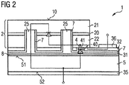
- the current paths in the semiconductor chip 1 are in Figure 2 shown schematically.
- the first semiconductor layer 21 and the carrier 5 are doped in an n-conductivity manner, for example, and the second semiconductor layer 22 is doped in a p-conductivity manner.
- the diode structure of the semiconductor body 2 provided for generating radiation is operated in the forward direction, so that Charge carriers are injected into the active area 20 and can recombine there with emissions of radiation.
- the protective diode 4 is switched in the reverse direction. No or at least no substantial proportion of the operating current flows through the transition layer 40 between the contacts 35, 36 of the semiconductor chip.
- the risk of damage to the semiconductor chip 1 can thus be reduced. It is thus possible to dispense with a protective diode which is embodied outside the semiconductor chip and which is connected in anti-parallel to the first contact 35 and second contact 36 of the semiconductor chip.
- the semiconductor chip can accordingly be operated in such a way that a positive voltage is present.
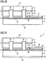
- FIG Figures 3A to 3E An exemplary embodiment of a method for producing a radiation-emitting semiconductor chip is shown in FIG Figures 3A to 3E shown on the basis of intermediate steps shown schematically in sectional view.
- a semiconductor body 2 which has a semiconductor layer sequence with an active region 20, a first semiconductor layer 21 and a second semiconductor layer 22 is provided.
- the semiconductor layer sequence which forms the semiconductor body 2 is preferably deposited epitaxially on a growth substrate 200.
- a second connection layer is formed on the second semiconductor layer 22. This can take place, for example, by means of vapor deposition or sputtering.
- the second connection layer 32 is formed locally structured, for example by means of lithographic techniques, in such a way that the second semiconductor layer 22 is exposed in regions.
- recesses 25 are formed in the semiconductor body 2, which extend through the second semiconductor layer 22 and the active region 20 into the first semiconductor layer 21.
- the semiconductor body 2 is then provided with an insulation layer 7 which covers the second connection layer 32 and in particular the side surfaces of the cutout 41 and the cutouts 25.
- a transition layer 40 is formed in the recess 41.
- the transition layer 40 can, for example be vapor-deposited or sputtered.
- a first connection layer 31 is subsequently deposited on the insulation layer 7, which extends into the recesses 25 and which furthermore directly adjoins the transition layer 40.
- the semiconductor body 2 can then be materially connected to a carrier 5. This can be done by means of a connecting layer 8, which can contain, for example, a solder or an electrically conductive adhesive.
- the semiconductor layer sequence of the semiconductor body 2 can be mechanically stabilized by means of the carrier 5.
- the growth substrate 200 is no longer required for this and can be removed.
- the growth substrate can be removed, for example, mechanically, for example by means of grinding, polishing or lapping and / or chemically, for example by means of wet-chemical or dry-chemical etching. Alternatively or in addition, a laser lift-off process can also be used.
- Material of the semiconductor body 2 is removed in areas in order to expose the second connection layer 32 in areas.
- a first contact 35 and a second contact 36 are deposited on the second main surface 52 of the carrier 5 facing away from the semiconductor body 2 and on the second connection layer 32. This can take place, for example, by means of vapor deposition or sputtering.
- the finished semiconductor chip, which as in the Connection with the Figures 1A and 1B is carried out is in Figure 3F shown.
- the integration of the protective diode 4 in the semiconductor chip 1 can be implemented in the described method without a significant additional expense.
- the electrical contact capability of the semiconductor body 2, in particular of the second semiconductor layer 22, can be locally reduced in a targeted manner prior to the deposition of the transition layer 40. This is preferably done before the first connection layer is deposited.
- the ability to contact can be reduced, for example, by incineration, for example in an O 2 plasma, or sputtering. In this way, the electrical conductivity can be reduced locally in a targeted manner in the region of the recess 41.
- the described method for production was shown only as an example for the production of a semiconductor chip.
- the Semiconductor layer sequence are provided on a wafer, wherein a plurality of semiconductor bodies can emerge from the semiconductor layer sequence by singulation.
- the separation can take place, for example, by means of sawing, breaking, cutting or etching.
Landscapes
- Led Devices (AREA)
- Electrodes Of Semiconductors (AREA)
- Semiconductor Lasers (AREA)
Applications Claiming Priority (3)
| Application Number | Priority Date | Filing Date | Title |
|---|---|---|---|
| DE102008034560.1A DE102008034560B4 (de) | 2008-07-24 | 2008-07-24 | Strahlungsemittierender Halbleiterchip und Verfahren zur Herstellung eines strahlungsemittierenden Halbleiterchips |
| EP09775907.0A EP2304799B1 (de) | 2008-07-24 | 2009-06-25 | Strahlungemittieren der halbleiterchip mit schutz gegen elektrostatische entladungen und entsprechendes herstellungsverfahren |
| PCT/DE2009/000885 WO2010009690A1 (de) | 2008-07-24 | 2009-06-25 | Strahlungemittierender halbleiterchip mit schutz gegen elektrostatische entladungen und entsprechendes herstellungsverfahren |
Related Parent Applications (2)
| Application Number | Title | Priority Date | Filing Date |
|---|---|---|---|
| EP09775907.0A Division EP2304799B1 (de) | 2008-07-24 | 2009-06-25 | Strahlungemittieren der halbleiterchip mit schutz gegen elektrostatische entladungen und entsprechendes herstellungsverfahren |
| EP09775907.0A Division-Into EP2304799B1 (de) | 2008-07-24 | 2009-06-25 | Strahlungemittieren der halbleiterchip mit schutz gegen elektrostatische entladungen und entsprechendes herstellungsverfahren |
Publications (2)
| Publication Number | Publication Date |
|---|---|
| EP3128555A1 EP3128555A1 (de) | 2017-02-08 |
| EP3128555B1 true EP3128555B1 (de) | 2021-08-18 |
Family
ID=41254639
Family Applications (2)
| Application Number | Title | Priority Date | Filing Date |
|---|---|---|---|
| EP16187828.5A Active EP3128555B1 (de) | 2008-07-24 | 2009-06-25 | Leuchtdiodenchip mit integriertem schutz gegen elektrostatische entladungen und entsprechendes herstellungsverfahren |
| EP09775907.0A Active EP2304799B1 (de) | 2008-07-24 | 2009-06-25 | Strahlungemittieren der halbleiterchip mit schutz gegen elektrostatische entladungen und entsprechendes herstellungsverfahren |
Family Applications After (1)
| Application Number | Title | Priority Date | Filing Date |
|---|---|---|---|
| EP09775907.0A Active EP2304799B1 (de) | 2008-07-24 | 2009-06-25 | Strahlungemittieren der halbleiterchip mit schutz gegen elektrostatische entladungen und entsprechendes herstellungsverfahren |
Country Status (7)
| Country | Link |
|---|---|
| US (1) | US8710537B2 (enExample) |
| EP (2) | EP3128555B1 (enExample) |
| JP (1) | JP5511813B2 (enExample) |
| KR (2) | KR101632082B1 (enExample) |
| CN (1) | CN101971344B (enExample) |
| DE (1) | DE102008034560B4 (enExample) |
| WO (1) | WO2010009690A1 (enExample) |
Families Citing this family (34)
| Publication number | Priority date | Publication date | Assignee | Title |
|---|---|---|---|---|
| DE102008034560B4 (de) | 2008-07-24 | 2022-10-27 | OSRAM Opto Semiconductors Gesellschaft mit beschränkter Haftung | Strahlungsemittierender Halbleiterchip und Verfahren zur Herstellung eines strahlungsemittierenden Halbleiterchips |
| DE102009006177A1 (de) * | 2008-11-28 | 2010-06-02 | Osram Opto Semiconductors Gmbh | Strahlungsemittierender Halbleiterchip |
| DE102009032486A1 (de) | 2009-07-09 | 2011-01-13 | Osram Opto Semiconductors Gmbh | Optoelektronisches Bauelement |
| DE102010013494A1 (de) | 2010-03-31 | 2011-10-06 | Osram Opto Semiconductors Gmbh | Optoelektronischer Halbleiterchip |
| DE102010027679A1 (de) | 2010-07-20 | 2012-01-26 | Osram Opto Semiconductors Gmbh | Optoelektronisches Bauelement |
| KR101692410B1 (ko) * | 2010-07-26 | 2017-01-03 | 삼성전자 주식회사 | 발광소자 및 그 제조방법 |
| KR101154320B1 (ko) * | 2010-12-20 | 2012-06-13 | 엘지이노텍 주식회사 | 발광소자, 발광소자 패키지 및 이를 포함하는 조명 장치 |
| TWI435477B (zh) * | 2010-12-29 | 2014-04-21 | Lextar Electronics Corp | 高亮度發光二極體 |
| DE102011011378B4 (de) * | 2011-02-16 | 2025-10-30 | OSRAM Opto Semiconductors Gesellschaft mit beschränkter Haftung | Halbleiterchip und Verfahren zur Herstellung von Halbleiterchips |
| TW201240146A (en) * | 2011-03-16 | 2012-10-01 | Hon Hai Prec Ind Co Ltd | Light-emitting semiconductor chip |
| TW201240147A (en) * | 2011-03-22 | 2012-10-01 | Hon Hai Prec Ind Co Ltd | Light-emitting semiconductor chip |
| CN102694098A (zh) * | 2011-03-25 | 2012-09-26 | 鸿富锦精密工业(深圳)有限公司 | 半导体发光芯片 |
| JP5887638B2 (ja) * | 2011-05-30 | 2016-03-16 | 億光電子工業股▲ふん▼有限公司Everlight Electronics Co.,Ltd. | 発光ダイオード |
| KR101973608B1 (ko) * | 2011-06-30 | 2019-04-29 | 엘지이노텍 주식회사 | 발광소자 |
| US9490239B2 (en) | 2011-08-31 | 2016-11-08 | Micron Technology, Inc. | Solid state transducers with state detection, and associated systems and methods |
| US8809897B2 (en) | 2011-08-31 | 2014-08-19 | Micron Technology, Inc. | Solid state transducer devices, including devices having integrated electrostatic discharge protection, and associated systems and methods |
| KR101868537B1 (ko) * | 2011-11-07 | 2018-06-19 | 엘지이노텍 주식회사 | 발광소자 및 이를 포함하는 발광 소자 패키지 |
| CN102522400B (zh) * | 2011-11-30 | 2014-11-26 | 晶科电子(广州)有限公司 | 一种防静电损伤的垂直发光器件及其制造方法 |
| DE102011056888A1 (de) | 2011-12-22 | 2013-06-27 | Osram Opto Semiconductors Gmbh | Anzeigevorrichtung und Verfahren zur Herstellung einer Anzeigevorrichtung |
| DE102012105176B4 (de) * | 2012-06-14 | 2021-08-12 | OSRAM Opto Semiconductors Gesellschaft mit beschränkter Haftung | Optoelektronischer Halbleiterchip |
| DE102012108627B4 (de) * | 2012-09-14 | 2021-06-10 | OSRAM Opto Semiconductors Gesellschaft mit beschränkter Haftung | Optoelektronische Halbleitervorrichtung und Trägerverbund |
| TWI661578B (zh) | 2013-06-20 | 2019-06-01 | Epistar Corporation | 發光裝置及發光陣列 |
| TWI536605B (zh) * | 2013-08-20 | 2016-06-01 | 隆達電子股份有限公司 | 發光二極體 |
| DE102013112881A1 (de) * | 2013-11-21 | 2015-05-21 | Osram Opto Semiconductors Gmbh | Optoelektronischer Halbleiterchip |
| JP6351531B2 (ja) | 2015-03-23 | 2018-07-04 | 株式会社東芝 | 半導体発光素子 |
| DE102015108532A1 (de) * | 2015-05-29 | 2016-12-01 | Osram Opto Semiconductors Gmbh | Anzeigevorrichtung mit einer Mehrzahl getrennt voneinander betreibbarer Bildpunkte |
| DE102015111485A1 (de) | 2015-07-15 | 2017-01-19 | Osram Opto Semiconductors Gmbh | Optoelektronisches Halbleiterbauelement |
| DE102015111487A1 (de) | 2015-07-15 | 2017-01-19 | Osram Opto Semiconductors Gmbh | Verfahren zur Herstellung eines optoelektronischen Halbleiterchips und optoelektronischer Halbleiterchip |
| DE102017104735B4 (de) | 2017-03-07 | 2021-09-02 | OSRAM Opto Semiconductors Gesellschaft mit beschränkter Haftung | Strahlungsemittierender Halbleiterchip |
| DE102017112223A1 (de) | 2017-06-02 | 2018-12-06 | Osram Opto Semiconductors Gmbh | Halbleiterlaser-Bauteil und Verfahren zur Herstellung eines Halbleiterlaser-Bauteils |
| DE102018119688B4 (de) * | 2018-08-14 | 2024-06-27 | OSRAM Opto Semiconductors Gesellschaft mit beschränkter Haftung | Optoelektronisches Halbleiterbauelement mit einem ersten Kontaktelement, welches einen ersten und einen zweiten Abschnitt aufweist sowie Verfahren zur Herstellung des optoelektronischen Halbleiterbauelements |
| WO2021038635A1 (ja) * | 2019-08-23 | 2021-03-04 | シャープ株式会社 | 発光素子、表示装置、および発光素子の製造方法 |
| JP7761771B2 (ja) * | 2022-02-08 | 2025-10-28 | エイエムエス-オスラム インターナショナル ゲーエムベーハー | レーザダイオード部品 |
| EP4328985A1 (en) | 2022-08-24 | 2024-02-28 | Albert-Ludwigs-Universität Freiburg | Micro led, neural implant, and method of fabricating a micro led |
Family Cites Families (18)
| Publication number | Priority date | Publication date | Assignee | Title |
|---|---|---|---|---|
| DE19945134C2 (de) | 1999-09-21 | 2003-08-14 | Osram Opto Semiconductors Gmbh | Lichtemittierendes Halbleiterbauelement hoher ESD-Festigkeit und Verfahren zu seiner Herstellung |
| TW492202B (en) | 2001-06-05 | 2002-06-21 | South Epitaxy Corp | Structure of III-V light emitting diode (LED) arranged in flip chip configuration having structure for preventing electrostatic discharge |
| DE10147886B4 (de) | 2001-09-28 | 2006-07-13 | Osram Opto Semiconductors Gmbh | Lumineszenzdiode mit vergrabenem Kontakt und Herstellungsverfahren |
| TWI220578B (en) | 2003-09-16 | 2004-08-21 | Opto Tech Corp | Light-emitting device capable of increasing light-emitting active region |
| DE102004005269B4 (de) | 2003-11-28 | 2005-09-29 | Osram Opto Semiconductors Gmbh | Lichtemittierendes Halbleiterbauelement mit einer Schutzdiode |
| TWI223457B (en) | 2004-01-20 | 2004-11-01 | Opto Tech Corp | Light-emitting device to increase the area of active region |
| US7064353B2 (en) | 2004-05-26 | 2006-06-20 | Philips Lumileds Lighting Company, Llc | LED chip with integrated fast switching diode for ESD protection |
| CN100386891C (zh) * | 2004-07-02 | 2008-05-07 | 北京工业大学 | 高抗静电高效发光二极管及制作方法 |
| JP2006086300A (ja) | 2004-09-15 | 2006-03-30 | Sanken Electric Co Ltd | 保護素子を有する半導体発光装置及びその製造方法 |
| KR100576872B1 (ko) | 2004-09-17 | 2006-05-10 | 삼성전기주식회사 | 정전기 방전 방지기능을 갖는 질화물 반도체 발광소자 |
| TWI244748B (en) * | 2004-10-08 | 2005-12-01 | Epistar Corp | A light-emitting device with a protecting structure |
| KR20060062715A (ko) * | 2004-12-06 | 2006-06-12 | 삼성전기주식회사 | 정전방전 보호 다이오드를 구비한 GaN 계열 반도체발광 소자 |
| US7754507B2 (en) * | 2005-06-09 | 2010-07-13 | Philips Lumileds Lighting Company, Llc | Method of removing the growth substrate of a semiconductor light emitting device |
| TWI257186B (en) | 2005-09-29 | 2006-06-21 | Formosa Epitaxy Inc | Light-emitting diode chip |
| US7994514B2 (en) | 2006-04-21 | 2011-08-09 | Koninklijke Philips Electronics N.V. | Semiconductor light emitting device with integrated electronic components |
| JP5044986B2 (ja) | 2006-05-17 | 2012-10-10 | サンケン電気株式会社 | 半導体発光装置 |
| CN100530622C (zh) | 2007-05-14 | 2009-08-19 | 金芃 | 垂直结构的半导体芯片或器件及制造方法 |
| DE102008034560B4 (de) | 2008-07-24 | 2022-10-27 | OSRAM Opto Semiconductors Gesellschaft mit beschränkter Haftung | Strahlungsemittierender Halbleiterchip und Verfahren zur Herstellung eines strahlungsemittierenden Halbleiterchips |
-
2008
- 2008-07-24 DE DE102008034560.1A patent/DE102008034560B4/de active Active
-
2009
- 2009-06-25 JP JP2011519023A patent/JP5511813B2/ja active Active
- 2009-06-25 US US12/922,736 patent/US8710537B2/en active Active
- 2009-06-25 EP EP16187828.5A patent/EP3128555B1/de active Active
- 2009-06-25 WO PCT/DE2009/000885 patent/WO2010009690A1/de not_active Ceased
- 2009-06-25 CN CN2009801090394A patent/CN101971344B/zh active Active
- 2009-06-25 KR KR1020107020375A patent/KR101632082B1/ko active Active
- 2009-06-25 KR KR1020167015687A patent/KR101710849B1/ko active Active
- 2009-06-25 EP EP09775907.0A patent/EP2304799B1/de active Active
Also Published As
| Publication number | Publication date |
|---|---|
| JP2011528855A (ja) | 2011-11-24 |
| CN101971344A (zh) | 2011-02-09 |
| EP3128555A1 (de) | 2017-02-08 |
| WO2010009690A1 (de) | 2010-01-28 |
| US20120018763A1 (en) | 2012-01-26 |
| EP2304799A1 (de) | 2011-04-06 |
| EP2304799B1 (de) | 2016-10-26 |
| US8710537B2 (en) | 2014-04-29 |
| KR101710849B1 (ko) | 2017-02-27 |
| DE102008034560B4 (de) | 2022-10-27 |
| KR20110031897A (ko) | 2011-03-29 |
| DE102008034560A1 (de) | 2010-02-04 |
| KR101632082B1 (ko) | 2016-06-20 |
| KR20160075810A (ko) | 2016-06-29 |
| JP5511813B2 (ja) | 2014-06-04 |
| CN101971344B (zh) | 2012-10-17 |
Similar Documents
| Publication | Publication Date | Title |
|---|---|---|
| EP3128555B1 (de) | Leuchtdiodenchip mit integriertem schutz gegen elektrostatische entladungen und entsprechendes herstellungsverfahren | |
| EP2274774B1 (de) | Strahlungsemittierender halbleiterchip | |
| EP2351079B1 (de) | Strahlungsemittierender halbleiterchip | |
| DE102010034665B4 (de) | Optoelektronischer Halbleiterchip und Verfahren zur Herstellung von optoelektronischen Halbleiterchips | |
| EP2015372B1 (de) | Halbleiterchip und Verfahren zur Herstellung eines Halbleiterchips | |
| EP2011160B1 (de) | Optoelektronischer halbleiterchip | |
| EP2583305B1 (de) | Verfahren zur herstellung eines optoelektronischen halbleiterchips und optoelektronischer halbleiterchip | |
| EP3200247B1 (de) | Halbleiterchip und verfahren zur herstellung eines halbleiterchips | |
| EP2149159B1 (de) | Optoelektronischer halbleiterkörper und verfahren zur herstellung eines solchen | |
| DE102007019775B4 (de) | Optoelektronisches Bauelement | |
| WO2011058094A1 (de) | Dünnfilm-halbleiterbauelement mit schutzdiodenstruktur und verfahren zur herstellung eines dünnfilm-halbleiterbauelements | |
| EP3381061B1 (de) | Leuchtdiodenchip mit einer reflektierenden schichtenfolge | |
| EP1906460A2 (de) | Halbleiterkörper und Halbleiterchip mit einem Halbleiterkörper | |
| WO2012110364A1 (de) | Optoelektronischer halbleiterchip und verfahren zur herstellung von optoelektronischen halbleiterchips | |
| EP2057696B1 (de) | Optoelektronischer halbleiterchip und verfahren zur dessen herstellung | |
| WO2012110365A1 (de) | Trägersubstrat und verfahren zur herstellung von halbleiterchips | |
| EP1592070B1 (de) | Strahlungsemittierendes und/oder -empfangendes Halbleiterbauelement und Verfahren zur strukturierten Aufbringung eines Kontakts auf einen Halbleiterkörper |
Legal Events
| Date | Code | Title | Description |
|---|---|---|---|
| PUAI | Public reference made under article 153(3) epc to a published international application that has entered the european phase |
Free format text: ORIGINAL CODE: 0009012 |
|
| STAA | Information on the status of an ep patent application or granted ep patent |
Free format text: STATUS: THE APPLICATION HAS BEEN PUBLISHED |
|
| AC | Divisional application: reference to earlier application |
Ref document number: 2304799 Country of ref document: EP Kind code of ref document: P |
|
| AK | Designated contracting states |
Kind code of ref document: A1 Designated state(s): AT BE BG CH CY CZ DE DK EE ES FI FR GB GR HR HU IE IS IT LI LT LU LV MC MK MT NL NO PL PT RO SE SI SK TR |
|
| STAA | Information on the status of an ep patent application or granted ep patent |
Free format text: STATUS: REQUEST FOR EXAMINATION WAS MADE |
|
| 17P | Request for examination filed |
Effective date: 20170803 |
|
| RBV | Designated contracting states (corrected) |
Designated state(s): AT BE BG CH CY CZ DE DK EE ES FI FR GB GR HR HU IE IS IT LI LT LU LV MC MK MT NL NO PL PT RO SE SI SK TR |
|
| RAP1 | Party data changed (applicant data changed or rights of an application transferred) |
Owner name: OSRAM OPTO SEMICONDUCTORS GMBH |
|
| GRAP | Despatch of communication of intention to grant a patent |
Free format text: ORIGINAL CODE: EPIDOSNIGR1 |
|
| STAA | Information on the status of an ep patent application or granted ep patent |
Free format text: STATUS: GRANT OF PATENT IS INTENDED |
|
| INTG | Intention to grant announced |
Effective date: 20210330 |
|
| GRAS | Grant fee paid |
Free format text: ORIGINAL CODE: EPIDOSNIGR3 |
|
| GRAA | (expected) grant |
Free format text: ORIGINAL CODE: 0009210 |
|
| STAA | Information on the status of an ep patent application or granted ep patent |
Free format text: STATUS: THE PATENT HAS BEEN GRANTED |
|
| AC | Divisional application: reference to earlier application |
Ref document number: 2304799 Country of ref document: EP Kind code of ref document: P |
|
| AK | Designated contracting states |
Kind code of ref document: B1 Designated state(s): AT BE BG CH CY CZ DE DK EE ES FI FR GB GR HR HU IE IS IT LI LT LU LV MC MK MT NL NO PL PT RO SE SI SK TR |
|
| REG | Reference to a national code |
Ref country code: GB Ref legal event code: FG4D Free format text: NOT ENGLISH |
|
| REG | Reference to a national code |
Ref country code: CH Ref legal event code: EP |
|
| REG | Reference to a national code |
Ref country code: DE Ref legal event code: R096 Ref document number: 502009016384 Country of ref document: DE |
|
| REG | Reference to a national code |
Ref country code: IE Ref legal event code: FG4D Free format text: LANGUAGE OF EP DOCUMENT: GERMAN Ref country code: AT Ref legal event code: REF Ref document number: 1422407 Country of ref document: AT Kind code of ref document: T Effective date: 20210915 |
|
| REG | Reference to a national code |
Ref country code: LT Ref legal event code: MG9D |
|
| REG | Reference to a national code |
Ref country code: NL Ref legal event code: MP Effective date: 20210818 |
|
| PG25 | Lapsed in a contracting state [announced via postgrant information from national office to epo] |
Ref country code: LT Free format text: LAPSE BECAUSE OF FAILURE TO SUBMIT A TRANSLATION OF THE DESCRIPTION OR TO PAY THE FEE WITHIN THE PRESCRIBED TIME-LIMIT Effective date: 20210818 Ref country code: BG Free format text: LAPSE BECAUSE OF FAILURE TO SUBMIT A TRANSLATION OF THE DESCRIPTION OR TO PAY THE FEE WITHIN THE PRESCRIBED TIME-LIMIT Effective date: 20211118 Ref country code: NO Free format text: LAPSE BECAUSE OF FAILURE TO SUBMIT A TRANSLATION OF THE DESCRIPTION OR TO PAY THE FEE WITHIN THE PRESCRIBED TIME-LIMIT Effective date: 20211118 Ref country code: PT Free format text: LAPSE BECAUSE OF FAILURE TO SUBMIT A TRANSLATION OF THE DESCRIPTION OR TO PAY THE FEE WITHIN THE PRESCRIBED TIME-LIMIT Effective date: 20211220 Ref country code: ES Free format text: LAPSE BECAUSE OF FAILURE TO SUBMIT A TRANSLATION OF THE DESCRIPTION OR TO PAY THE FEE WITHIN THE PRESCRIBED TIME-LIMIT Effective date: 20210818 Ref country code: FI Free format text: LAPSE BECAUSE OF FAILURE TO SUBMIT A TRANSLATION OF THE DESCRIPTION OR TO PAY THE FEE WITHIN THE PRESCRIBED TIME-LIMIT Effective date: 20210818 Ref country code: SE Free format text: LAPSE BECAUSE OF FAILURE TO SUBMIT A TRANSLATION OF THE DESCRIPTION OR TO PAY THE FEE WITHIN THE PRESCRIBED TIME-LIMIT Effective date: 20210818 Ref country code: HR Free format text: LAPSE BECAUSE OF FAILURE TO SUBMIT A TRANSLATION OF THE DESCRIPTION OR TO PAY THE FEE WITHIN THE PRESCRIBED TIME-LIMIT Effective date: 20210818 |
|
| PG25 | Lapsed in a contracting state [announced via postgrant information from national office to epo] |
Ref country code: PL Free format text: LAPSE BECAUSE OF FAILURE TO SUBMIT A TRANSLATION OF THE DESCRIPTION OR TO PAY THE FEE WITHIN THE PRESCRIBED TIME-LIMIT Effective date: 20210818 Ref country code: LV Free format text: LAPSE BECAUSE OF FAILURE TO SUBMIT A TRANSLATION OF THE DESCRIPTION OR TO PAY THE FEE WITHIN THE PRESCRIBED TIME-LIMIT Effective date: 20210818 Ref country code: GR Free format text: LAPSE BECAUSE OF FAILURE TO SUBMIT A TRANSLATION OF THE DESCRIPTION OR TO PAY THE FEE WITHIN THE PRESCRIBED TIME-LIMIT Effective date: 20211119 |
|
| PG25 | Lapsed in a contracting state [announced via postgrant information from national office to epo] |
Ref country code: NL Free format text: LAPSE BECAUSE OF FAILURE TO SUBMIT A TRANSLATION OF THE DESCRIPTION OR TO PAY THE FEE WITHIN THE PRESCRIBED TIME-LIMIT Effective date: 20210818 |
|
| PG25 | Lapsed in a contracting state [announced via postgrant information from national office to epo] |
Ref country code: DK Free format text: LAPSE BECAUSE OF FAILURE TO SUBMIT A TRANSLATION OF THE DESCRIPTION OR TO PAY THE FEE WITHIN THE PRESCRIBED TIME-LIMIT Effective date: 20210818 |
|
| REG | Reference to a national code |
Ref country code: DE Ref legal event code: R097 Ref document number: 502009016384 Country of ref document: DE |
|
| PG25 | Lapsed in a contracting state [announced via postgrant information from national office to epo] |
Ref country code: SK Free format text: LAPSE BECAUSE OF FAILURE TO SUBMIT A TRANSLATION OF THE DESCRIPTION OR TO PAY THE FEE WITHIN THE PRESCRIBED TIME-LIMIT Effective date: 20210818 Ref country code: RO Free format text: LAPSE BECAUSE OF FAILURE TO SUBMIT A TRANSLATION OF THE DESCRIPTION OR TO PAY THE FEE WITHIN THE PRESCRIBED TIME-LIMIT Effective date: 20210818 Ref country code: EE Free format text: LAPSE BECAUSE OF FAILURE TO SUBMIT A TRANSLATION OF THE DESCRIPTION OR TO PAY THE FEE WITHIN THE PRESCRIBED TIME-LIMIT Effective date: 20210818 Ref country code: CZ Free format text: LAPSE BECAUSE OF FAILURE TO SUBMIT A TRANSLATION OF THE DESCRIPTION OR TO PAY THE FEE WITHIN THE PRESCRIBED TIME-LIMIT Effective date: 20210818 |
|
| PLBE | No opposition filed within time limit |
Free format text: ORIGINAL CODE: 0009261 |
|
| STAA | Information on the status of an ep patent application or granted ep patent |
Free format text: STATUS: NO OPPOSITION FILED WITHIN TIME LIMIT |
|
| 26N | No opposition filed |
Effective date: 20220519 |
|
| PG25 | Lapsed in a contracting state [announced via postgrant information from national office to epo] |
Ref country code: IT Free format text: LAPSE BECAUSE OF FAILURE TO SUBMIT A TRANSLATION OF THE DESCRIPTION OR TO PAY THE FEE WITHIN THE PRESCRIBED TIME-LIMIT Effective date: 20210818 |
|
| PG25 | Lapsed in a contracting state [announced via postgrant information from national office to epo] |
Ref country code: SI Free format text: LAPSE BECAUSE OF FAILURE TO SUBMIT A TRANSLATION OF THE DESCRIPTION OR TO PAY THE FEE WITHIN THE PRESCRIBED TIME-LIMIT Effective date: 20210818 |
|
| PG25 | Lapsed in a contracting state [announced via postgrant information from national office to epo] |
Ref country code: MC Free format text: LAPSE BECAUSE OF FAILURE TO SUBMIT A TRANSLATION OF THE DESCRIPTION OR TO PAY THE FEE WITHIN THE PRESCRIBED TIME-LIMIT Effective date: 20210818 |
|
| REG | Reference to a national code |
Ref country code: CH Ref legal event code: PL |
|
| REG | Reference to a national code |
Ref country code: BE Ref legal event code: MM Effective date: 20220630 |
|
| GBPC | Gb: european patent ceased through non-payment of renewal fee |
Effective date: 20220625 |
|
| PG25 | Lapsed in a contracting state [announced via postgrant information from national office to epo] |
Ref country code: LI Free format text: LAPSE BECAUSE OF NON-PAYMENT OF DUE FEES Effective date: 20220630 Ref country code: IE Free format text: LAPSE BECAUSE OF NON-PAYMENT OF DUE FEES Effective date: 20220625 Ref country code: FR Free format text: LAPSE BECAUSE OF NON-PAYMENT OF DUE FEES Effective date: 20220630 Ref country code: CH Free format text: LAPSE BECAUSE OF NON-PAYMENT OF DUE FEES Effective date: 20220630 Ref country code: LU Free format text: LAPSE BECAUSE OF NON-PAYMENT OF DUE FEES Effective date: 20220625 |
|
| PG25 | Lapsed in a contracting state [announced via postgrant information from national office to epo] |
Ref country code: GB Free format text: LAPSE BECAUSE OF NON-PAYMENT OF DUE FEES Effective date: 20220625 Ref country code: BE Free format text: LAPSE BECAUSE OF NON-PAYMENT OF DUE FEES Effective date: 20220630 |
|
| REG | Reference to a national code |
Ref country code: AT Ref legal event code: MM01 Ref document number: 1422407 Country of ref document: AT Kind code of ref document: T Effective date: 20220625 |
|
| P01 | Opt-out of the competence of the unified patent court (upc) registered |
Effective date: 20230825 |
|
| PG25 | Lapsed in a contracting state [announced via postgrant information from national office to epo] |
Ref country code: AT Free format text: LAPSE BECAUSE OF NON-PAYMENT OF DUE FEES Effective date: 20220625 |
|
| PG25 | Lapsed in a contracting state [announced via postgrant information from national office to epo] |
Ref country code: HU Free format text: LAPSE BECAUSE OF FAILURE TO SUBMIT A TRANSLATION OF THE DESCRIPTION OR TO PAY THE FEE WITHIN THE PRESCRIBED TIME-LIMIT; INVALID AB INITIO Effective date: 20090625 |
|
| PG25 | Lapsed in a contracting state [announced via postgrant information from national office to epo] |
Ref country code: MK Free format text: LAPSE BECAUSE OF FAILURE TO SUBMIT A TRANSLATION OF THE DESCRIPTION OR TO PAY THE FEE WITHIN THE PRESCRIBED TIME-LIMIT Effective date: 20210818 Ref country code: CY Free format text: LAPSE BECAUSE OF FAILURE TO SUBMIT A TRANSLATION OF THE DESCRIPTION OR TO PAY THE FEE WITHIN THE PRESCRIBED TIME-LIMIT Effective date: 20210818 |
|
| PG25 | Lapsed in a contracting state [announced via postgrant information from national office to epo] |
Ref country code: TR Free format text: LAPSE BECAUSE OF FAILURE TO SUBMIT A TRANSLATION OF THE DESCRIPTION OR TO PAY THE FEE WITHIN THE PRESCRIBED TIME-LIMIT Effective date: 20210818 |
|
| PG25 | Lapsed in a contracting state [announced via postgrant information from national office to epo] |
Ref country code: MT Free format text: LAPSE BECAUSE OF FAILURE TO SUBMIT A TRANSLATION OF THE DESCRIPTION OR TO PAY THE FEE WITHIN THE PRESCRIBED TIME-LIMIT Effective date: 20210818 |
|
| REG | Reference to a national code |
Ref country code: DE Ref legal event code: R079 Ref document number: 502009016384 Country of ref document: DE Free format text: PREVIOUS MAIN CLASS: H01L0027150000 Ipc: H10H0029140000 |
|
| PGFP | Annual fee paid to national office [announced via postgrant information from national office to epo] |
Ref country code: DE Payment date: 20250618 Year of fee payment: 17 |