EP3128555B1 - Light-emitting semi-conductor chip with integrated esd protection and a method for producing a light-emitting semiconductor chip - Google Patents
Light-emitting semi-conductor chip with integrated esd protection and a method for producing a light-emitting semiconductor chip Download PDFInfo
- Publication number
- EP3128555B1 EP3128555B1 EP16187828.5A EP16187828A EP3128555B1 EP 3128555 B1 EP3128555 B1 EP 3128555B1 EP 16187828 A EP16187828 A EP 16187828A EP 3128555 B1 EP3128555 B1 EP 3128555B1
- Authority
- EP
- European Patent Office
- Prior art keywords
- layer
- semiconductor
- semiconductor layer
- radiation
- semiconductor chip
- Prior art date
- Legal status (The legal status is an assumption and is not a legal conclusion. Google has not performed a legal analysis and makes no representation as to the accuracy of the status listed.)
- Active
Links
- 239000004065 semiconductor Substances 0.000 title claims description 279
- 238000004519 manufacturing process Methods 0.000 title claims description 12
- 230000001681 protective effect Effects 0.000 claims description 46
- 230000005855 radiation Effects 0.000 claims description 40
- 230000007704 transition Effects 0.000 claims description 35
- 238000000034 method Methods 0.000 claims description 14
- 239000000758 substrate Substances 0.000 claims description 11
- 238000004544 sputter deposition Methods 0.000 claims description 7
- 238000004380 ashing Methods 0.000 claims description 3
- 239000010410 layer Substances 0.000 description 223
- 239000000463 material Substances 0.000 description 24
- 239000002800 charge carrier Substances 0.000 description 12
- 230000006378 damage Effects 0.000 description 8
- 238000011161 development Methods 0.000 description 6
- 230000018109 developmental process Effects 0.000 description 6
- 238000009413 insulation Methods 0.000 description 6
- 239000010409 thin film Substances 0.000 description 5
- 229910052782 aluminium Inorganic materials 0.000 description 4
- 230000001427 coherent effect Effects 0.000 description 4
- 229910052751 metal Inorganic materials 0.000 description 4
- 239000002184 metal Substances 0.000 description 4
- 229910052697 platinum Inorganic materials 0.000 description 4
- 229910052709 silver Inorganic materials 0.000 description 4
- XUIMIQQOPSSXEZ-UHFFFAOYSA-N Silicon Chemical compound [Si] XUIMIQQOPSSXEZ-UHFFFAOYSA-N 0.000 description 3
- 239000012876 carrier material Substances 0.000 description 3
- 238000002310 reflectometry Methods 0.000 description 3
- 229910052710 silicon Inorganic materials 0.000 description 3
- 239000010703 silicon Substances 0.000 description 3
- 230000003595 spectral effect Effects 0.000 description 3
- 238000007740 vapor deposition Methods 0.000 description 3
- JBRZTFJDHDCESZ-UHFFFAOYSA-N AsGa Chemical compound [As]#[Ga] JBRZTFJDHDCESZ-UHFFFAOYSA-N 0.000 description 2
- 229910002601 GaN Inorganic materials 0.000 description 2
- 229910001218 Gallium arsenide Inorganic materials 0.000 description 2
- JMASRVWKEDWRBT-UHFFFAOYSA-N Gallium nitride Chemical compound [Ga]#N JMASRVWKEDWRBT-UHFFFAOYSA-N 0.000 description 2
- XLOMVQKBTHCTTD-UHFFFAOYSA-N Zinc monoxide Chemical compound [Zn]=O XLOMVQKBTHCTTD-UHFFFAOYSA-N 0.000 description 2
- XAGFODPZIPBFFR-UHFFFAOYSA-N aluminium Chemical compound [Al] XAGFODPZIPBFFR-UHFFFAOYSA-N 0.000 description 2
- 239000000919 ceramic Substances 0.000 description 2
- 238000007786 electrostatic charging Methods 0.000 description 2
- 229910052732 germanium Inorganic materials 0.000 description 2
- GNPVGFCGXDBREM-UHFFFAOYSA-N germanium atom Chemical compound [Ge] GNPVGFCGXDBREM-UHFFFAOYSA-N 0.000 description 2
- 229910052737 gold Inorganic materials 0.000 description 2
- 229910001092 metal group alloy Inorganic materials 0.000 description 2
- 238000002488 metal-organic chemical vapour deposition Methods 0.000 description 2
- 229910052759 nickel Inorganic materials 0.000 description 2
- 230000005693 optoelectronics Effects 0.000 description 2
- 229910052763 palladium Inorganic materials 0.000 description 2
- 229910052703 rhodium Inorganic materials 0.000 description 2
- 239000004332 silver Substances 0.000 description 2
- 229910000679 solder Inorganic materials 0.000 description 2
- 229910052719 titanium Inorganic materials 0.000 description 2
- 239000010936 titanium Substances 0.000 description 2
- 229910052721 tungsten Inorganic materials 0.000 description 2
- 229910052582 BN Inorganic materials 0.000 description 1
- PZNSFCLAULLKQX-UHFFFAOYSA-N Boron nitride Chemical compound N#B PZNSFCLAULLKQX-UHFFFAOYSA-N 0.000 description 1
- 229910052581 Si3N4 Inorganic materials 0.000 description 1
- VYPSYNLAJGMNEJ-UHFFFAOYSA-N Silicium dioxide Chemical compound O=[Si]=O VYPSYNLAJGMNEJ-UHFFFAOYSA-N 0.000 description 1
- GWEVSGVZZGPLCZ-UHFFFAOYSA-N Titan oxide Chemical compound O=[Ti]=O GWEVSGVZZGPLCZ-UHFFFAOYSA-N 0.000 description 1
- 238000010521 absorption reaction Methods 0.000 description 1
- 239000000853 adhesive Substances 0.000 description 1
- 230000001070 adhesive effect Effects 0.000 description 1
- 239000012790 adhesive layer Substances 0.000 description 1
- QVGXLLKOCUKJST-UHFFFAOYSA-N atomic oxygen Chemical compound [O] QVGXLLKOCUKJST-UHFFFAOYSA-N 0.000 description 1
- 230000015572 biosynthetic process Effects 0.000 description 1
- 238000003486 chemical etching Methods 0.000 description 1
- PMHQVHHXPFUNSP-UHFFFAOYSA-M copper(1+);methylsulfanylmethane;bromide Chemical compound Br[Cu].CSC PMHQVHHXPFUNSP-UHFFFAOYSA-M 0.000 description 1
- 238000005520 cutting process Methods 0.000 description 1
- 230000001419 dependent effect Effects 0.000 description 1
- 238000000151 deposition Methods 0.000 description 1
- 230000008021 deposition Effects 0.000 description 1
- 238000009826 distribution Methods 0.000 description 1
- 238000005530 etching Methods 0.000 description 1
- 238000000227 grinding Methods 0.000 description 1
- 229910003437 indium oxide Inorganic materials 0.000 description 1
- PJXISJQVUVHSOJ-UHFFFAOYSA-N indium(iii) oxide Chemical compound [O-2].[O-2].[O-2].[In+3].[In+3] PJXISJQVUVHSOJ-UHFFFAOYSA-N 0.000 description 1
- AMGQUBHHOARCQH-UHFFFAOYSA-N indium;oxotin Chemical compound [In].[Sn]=O AMGQUBHHOARCQH-UHFFFAOYSA-N 0.000 description 1
- 238000002347 injection Methods 0.000 description 1
- 239000007924 injection Substances 0.000 description 1
- 230000010354 integration Effects 0.000 description 1
- 238000002955 isolation Methods 0.000 description 1
- 239000011159 matrix material Substances 0.000 description 1
- 150000002739 metals Chemical class 0.000 description 1
- 238000002156 mixing Methods 0.000 description 1
- 239000000203 mixture Substances 0.000 description 1
- 150000004767 nitrides Chemical class 0.000 description 1
- 230000003287 optical effect Effects 0.000 description 1
- 229910052760 oxygen Inorganic materials 0.000 description 1
- 239000001301 oxygen Substances 0.000 description 1
- 238000005498 polishing Methods 0.000 description 1
- 238000005036 potential barrier Methods 0.000 description 1
- 230000000717 retained effect Effects 0.000 description 1
- 230000035945 sensitivity Effects 0.000 description 1
- 238000000926 separation method Methods 0.000 description 1
- HQVNEWCFYHHQES-UHFFFAOYSA-N silicon nitride Chemical compound N12[Si]34N5[Si]62N3[Si]51N64 HQVNEWCFYHHQES-UHFFFAOYSA-N 0.000 description 1
- 229910052814 silicon oxide Inorganic materials 0.000 description 1
- 239000000126 substance Substances 0.000 description 1
- OGIDPMRJRNCKJF-UHFFFAOYSA-N titanium oxide Inorganic materials [Ti]=O OGIDPMRJRNCKJF-UHFFFAOYSA-N 0.000 description 1
- 239000011787 zinc oxide Substances 0.000 description 1
Images


Classifications
-
- H—ELECTRICITY
- H01—ELECTRIC ELEMENTS
- H01L—SEMICONDUCTOR DEVICES NOT COVERED BY CLASS H10
- H01L27/00—Devices consisting of a plurality of semiconductor or other solid-state components formed in or on a common substrate
- H01L27/15—Devices consisting of a plurality of semiconductor or other solid-state components formed in or on a common substrate including semiconductor components with at least one potential-jump barrier or surface barrier specially adapted for light emission
-
- H—ELECTRICITY
- H01—ELECTRIC ELEMENTS
- H01L—SEMICONDUCTOR DEVICES NOT COVERED BY CLASS H10
- H01L27/00—Devices consisting of a plurality of semiconductor or other solid-state components formed in or on a common substrate
- H01L27/02—Devices consisting of a plurality of semiconductor or other solid-state components formed in or on a common substrate including semiconductor components specially adapted for rectifying, oscillating, amplifying or switching and having at least one potential-jump barrier or surface barrier; including integrated passive circuit elements with at least one potential-jump barrier or surface barrier
- H01L27/0203—Particular design considerations for integrated circuits
- H01L27/0248—Particular design considerations for integrated circuits for electrical or thermal protection, e.g. electrostatic discharge [ESD] protection
- H01L27/0251—Particular design considerations for integrated circuits for electrical or thermal protection, e.g. electrostatic discharge [ESD] protection for MOS devices
- H01L27/0255—Particular design considerations for integrated circuits for electrical or thermal protection, e.g. electrostatic discharge [ESD] protection for MOS devices using diodes as protective elements
-
- H—ELECTRICITY
- H01—ELECTRIC ELEMENTS
- H01L—SEMICONDUCTOR DEVICES NOT COVERED BY CLASS H10
- H01L33/00—Semiconductor devices with at least one potential-jump barrier or surface barrier specially adapted for light emission; Processes or apparatus specially adapted for the manufacture or treatment thereof or of parts thereof; Details thereof
- H01L33/02—Semiconductor devices with at least one potential-jump barrier or surface barrier specially adapted for light emission; Processes or apparatus specially adapted for the manufacture or treatment thereof or of parts thereof; Details thereof characterised by the semiconductor bodies
-
- H—ELECTRICITY
- H01—ELECTRIC ELEMENTS
- H01L—SEMICONDUCTOR DEVICES NOT COVERED BY CLASS H10
- H01L33/00—Semiconductor devices with at least one potential-jump barrier or surface barrier specially adapted for light emission; Processes or apparatus specially adapted for the manufacture or treatment thereof or of parts thereof; Details thereof
- H01L33/36—Semiconductor devices with at least one potential-jump barrier or surface barrier specially adapted for light emission; Processes or apparatus specially adapted for the manufacture or treatment thereof or of parts thereof; Details thereof characterised by the electrodes
- H01L33/38—Semiconductor devices with at least one potential-jump barrier or surface barrier specially adapted for light emission; Processes or apparatus specially adapted for the manufacture or treatment thereof or of parts thereof; Details thereof characterised by the electrodes with a particular shape
- H01L33/382—Semiconductor devices with at least one potential-jump barrier or surface barrier specially adapted for light emission; Processes or apparatus specially adapted for the manufacture or treatment thereof or of parts thereof; Details thereof characterised by the electrodes with a particular shape the electrode extending partially in or entirely through the semiconductor body
-
- H—ELECTRICITY
- H01—ELECTRIC ELEMENTS
- H01L—SEMICONDUCTOR DEVICES NOT COVERED BY CLASS H10
- H01L33/00—Semiconductor devices with at least one potential-jump barrier or surface barrier specially adapted for light emission; Processes or apparatus specially adapted for the manufacture or treatment thereof or of parts thereof; Details thereof
- H01L33/48—Semiconductor devices with at least one potential-jump barrier or surface barrier specially adapted for light emission; Processes or apparatus specially adapted for the manufacture or treatment thereof or of parts thereof; Details thereof characterised by the semiconductor body packages
- H01L33/62—Arrangements for conducting electric current to or from the semiconductor body, e.g. lead-frames, wire-bonds or solder balls
-
- H—ELECTRICITY
- H01—ELECTRIC ELEMENTS
- H01L—SEMICONDUCTOR DEVICES NOT COVERED BY CLASS H10
- H01L2924/00—Indexing scheme for arrangements or methods for connecting or disconnecting semiconductor or solid-state bodies as covered by H01L24/00
- H01L2924/0001—Technical content checked by a classifier
- H01L2924/0002—Not covered by any one of groups H01L24/00, H01L24/00 and H01L2224/00
Definitions
- the present application relates to a radiation-emitting semiconductor chip and a method for producing a radiation-emitting semiconductor chip.
- a radiation-emitting semiconductor chip has a carrier and a semiconductor body with a semiconductor layer sequence.
- the semiconductor layer sequence has an active region provided for generating radiation, a first semiconductor layer and a second semiconductor layer.
- the active area is arranged between the first semiconductor layer and the second semiconductor layer.
- the first semiconductor layer is arranged on the side of the active region facing away from the carrier.
- the semiconductor body has at least one recess which extends through the active region.
- the first semiconductor layer is connected in an electrically conductive manner to a first connection layer, the first connection layer extending in the recess from the first semiconductor layer in the direction of the carrier.
- the first connection layer is electrically connected to the second semiconductor layer via a protective diode.
- the protective diode is integrated into the semiconductor chip.
- the risk of damage to the semiconductor chip, for example due to electrostatic discharge, is thus reduced.
- An additional protective diode to be arranged outside the semiconductor chip and connected to it in an electrically conductive manner can be dispensed with.
- the protective diode can in particular fulfill the function of an ESD (Electrostatic Discharge) diode which protects the semiconductor chip from damage by electrostatic discharge.
- ESD Electrostatic Discharge
- charge carriers can flow away via a current path between the first connection layer and the second semiconductor layer. The risk of damage to the semiconductor chip can thus be reduced.
- the first semiconductor layer and the second semiconductor layer of the semiconductor body are expediently different from one another with regard to their conductivity type.
- the first semiconductor layer can be p-conductive and the second semiconductor layer n-conductive, or vice versa.
- a diode structure in which the active area is formed is thus implemented in a simple manner.
- the protective diode is formed between the first connection layer and the second semiconductor layer.
- the protective diode can thus be arranged in a simple manner in a current path between the first connection layer and the second semiconductor layer.
- the protective diode can be formed outside the carrier.
- the protective diode can thus be formed largely independently of the properties of the carrier, in particular the electrical conductivity or the electrical contactability.
- the semiconductor chip furthermore preferably has a first contact and a second contact, which are each provided for the external electrical contacting of the semiconductor chip.
- An operating voltage applied between the first contact and the second contact causes charge carriers to be injected into the active area from different sides of the active area.
- the injected charge carriers can recombine with the emission of radiation in the active area.
- the diode structure of the semiconductor body and the protective diode are expediently formed antiparallel to one another.
- the protective diode is designed as a Schottky diode.
- a Schottky diode can in particular be formed by means of a metal-semiconductor junction, the current-voltage characteristic of the junction deviating from an ohmic characteristic and, in particular, running asymmetrically with respect to the polarity of the applied voltage.
- the protective diode overlaps with the semiconductor body in a plan view of the semiconductor chip.
- the semiconductor body in particular the active area, can completely cover the protective diode in plan view.
- the protective diode can thus be integrated into the semiconductor chip with the same lateral extent of the semiconductor body. Furthermore, the protective diode can thus be integrated into the semiconductor chip while maintaining the area of the active region that can be used for generating radiation.
- a lateral direction is understood to mean a direction which runs along a main plane of extent of the semiconductor layers of the semiconductor body.
- the protective diode is formed by means of the second semiconductor layer.
- the second semiconductor layer can therefore be provided both for the injection of charge carriers into the active region and for the formation of the protective diode.
- a separate semiconductor region, which is electrically isolated from the active region, for forming the Schottky diode can thus be dispensed with.
- the protective diode in particular in the form of a Schottky diode, can be integrated into the semiconductor chip with the same lateral extent of the semiconductor chip, without reducing the area of the active region that is decisive for generating radiation.
- the protection diode can thus be integrated into the semiconductor chip without impairing the optoelectronic properties of the semiconductor chip.
- the first connection layer runs at least in some areas between the carrier and the second semiconductor layer.
- electrical contact can be made with the first semiconductor layer from the side of the active region facing the carrier.
- a second connection layer is arranged at least in regions between the first connection layer and the second semiconductor layer.
- the second connection layer is connected in an electrically conductive manner to the second semiconductor layer and furthermore preferably directly adjoins the second semiconductor layer.
- the first connection layer and the second connection layer can each be electrically contacted externally via the first and second contact, respectively.
- the first and / or the second contact can each be formed by means of a contact layer which is arranged, preferably directly, on the first or second connection layer.
- the first connection layer can form the first contact and / or the second connection layer can form the second contact.
- at least one separate contact layer which is provided in addition to the connection layers and forms the first or second contact, can be dispensed with.
- the first connection layer and / or the second connection layer preferably each contain a metal, for example Ti, Pt, Ni, Au, Ag, Al, Rh, Pd, Pt or W or a metallic alloy with at least one of the materials mentioned.
- the first and / or the second connection layer are preferably arranged outside the semiconductor body and fabricated by a non-epitaxial process such as vapor deposition or sputtering.
- the protective diode is formed by means of a transition layer which is arranged on the second semiconductor layer and furthermore preferably adjoins the second semiconductor layer.
- the transition layer and the second connection layer are expediently spaced apart from one another in the lateral direction. A direct electrical contact between the transition layer and the second connection layer can thus be avoided in a simple manner.
- an insulation layer is preferably formed between the transition layer and the second connection layer. The risk of an electrical short circuit between the transition layer and the second connection layer can thus be further reduced.
- the transition layer is preferably selected in such a way that a Schottky transition, that is to say a metal-semiconductor transition with asymmetrical current-voltage characteristics, to the second semiconductor layer can be implemented in a simplified manner.
- the protective diode is formed by means of the first connection layer, the first connection layer preferably adjoining the second semiconductor layer.
- the first connection layer adjoins the first semiconductor layer and the second semiconductor layer, with an ohmic or at least approximately ohmic contact between the first connection layer and the first contact layer and between a Schottky contact is formed between the first connection layer and the second contact layer.
- the material for the layer adjoining the second semiconductor layer is preferably selected such that a Schottky contact to the second semiconductor layer can be formed in a simplified manner.
- the second semiconductor layer has, at least in some areas, in particular in the area of the protective diode, a locally targeted reduced contact capability.
- a locally targeted reduced contact capability can be produced, for example, by ashing, for example in an oxygen-containing plasma, or by sputtering. In this way, the electrical conductivity of the second semiconductor layer can be reduced in a targeted manner.
- the layer can contain a material or consist of a material which has a high reflectivity for the radiation generated in the active region.
- a material or consist of a material which has a high reflectivity for the radiation generated in the active region For radiation in the visible or in the ultraviolet spectral range, for example, silver or aluminum are characterized by a high reflectivity.
- the first contact and the second contact are formed on different sides of the carrier.
- the carrier is preferably designed to be electrically conductive.
- the first contact and the second contact are arranged on the side of the carrier facing the semiconductor body.
- the carrier can be selected independently of its electrical conductivity and, in particular, can be designed to be electrically insulating.
- a preferably doped semiconductor material is suitable as the electrically conductive carrier material.
- the carrier can contain silicon, germanium, gallium arsenide or gallium nitride or consist of such a material.
- a ceramic for example aluminum nitride or boron nitride, is also suitable as a carrier material.
- a carrier can be designed to be electrically insulating.
- the semiconductor body is preferably materially connected to the carrier.
- the carrier is in particular different from a growth substrate for the semiconductor layer sequence of the semiconductor body.
- the carrier preferably mechanically stabilizes the semiconductor layer sequence of the semiconductor body.
- the growth substrate of the semiconductor body is not required for this and can be removed.
- connection partners which are preferably prefabricated, are connected by means of held together by atomic and / or molecular forces.
- a material connection can be achieved, for example, by means of a connection layer, for example an adhesive layer or a solder layer.
- a disconnection is accompanied by the destruction of the connection layer and / or at least one of the connection partners.
- the growth substrate for the semiconductor layer sequence of the semiconductor body is removed at least in some areas.
- the growth substrate can be thinned over the entire area or in areas or removed over the entire area or in areas.
- a semiconductor chip from which the growth substrate has been removed is also referred to as a thin-film semiconductor chip.
- the semiconductor layer sequence of the semiconductor body is preferably deposited epitaxially, for example by means of MOVPE or MBE.
- the semiconductor body in particular the active region, preferably contains a III-V semiconductor material.
- III-V semiconductor materials high internal quantum efficiencies can be achieved when generating radiation.
- the structure described is generally suitable for optoelectronic semiconductor chips which are provided for generating radiation and / or for detecting radiation.
- the semiconductor chip can be provided for generating incoherent, partially coherent or coherent radiation.
- a structure based on an LED chip is suitable for generating incoherent radiation, for example, and a structure based on an RCLED chip (Resonant Cavity Light Emitting Diode) is suitable for generating partially coherent radiation.
- Coherent Radiation can be generated, for example, by means of a semiconductor laser chip, which in particular is used as a edge-emitting laser or as a surface-emitting laser, for example as a VCSEL (vertical cavity surface emitting laser) or as a VECSEL (vertical external cavity surface emitting laser).
- radiation-emitting semiconductor chips are provided with a semiconductor body with a semiconductor layer sequence which has an active region provided for generating radiation, a first semiconductor layer and a second semiconductor layer.
- a recess is formed in the semiconductor body which extends through the active region into the first semiconductor layer.
- a first connection layer is formed on the semiconductor body, the first connection layer extending into the recess. The first connection layer is electrically connected to the second semiconductor layer via a protective diode.
- the semiconductor chip is completed.
- a method in which a protective diode can be integrated into the semiconductor chip is thus implemented in a simple and inexpensive manner. With this method, a large number of semiconductor chips can be produced simultaneously, in particular next to one another on a wafer. With this method, semiconductor chips can be produced through isolation in which a protective diode is already integrated.
- the protection diode can thus be integrated at the wafer level, that is, before the semiconductor chips are singulated.
- a transition layer is formed which adjoins the second semiconductor layer.
- a Schottky diode can be formed by means of the transition layer.
- the electrical contactability of the second semiconductor layer is specifically reduced locally. This can take place in particular before the transition layer is deposited.
- the electrical contact capability can be reduced by ashing and / or by sputtering.
- the second connection layer is exposed by removing the semiconductor body in regions. In the exposed region of the second connection layer, a contact can be formed which is provided for making electrical contact with the semiconductor chip.
- the method described is particularly suitable for producing a radiation-emitting semiconductor chip described above.
- the features described in connection with the method can therefore also be used for the semiconductor chip and vice versa.
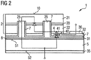
- a first embodiment for one radiation-emitting semiconductor chip is schematically based on a plan in Figure 1B and an associated sectional view along the line AA 'in FIG Figure 1A shown.
- the radiation-emitting semiconductor chip 1 has a semiconductor body 2 which is fastened to a carrier 5 by means of a connecting layer 8.
- the semiconductor layer sequence which forms the semiconductor body 2 is preferably produced epitaxially, for example by means of MOVPE or MBE.
- the semiconductor body has an active region 20 which is provided for generating radiation and which is arranged between a first semiconductor layer 21 and a second semiconductor layer 22.
- the first semiconductor layer 21 and the second semiconductor layer 22 are different from each other in terms of their conductivity type.
- the second semiconductor layer 22 can be designed to be p-conductive and the first semiconductor layer 21 to be n-conductive, or vice versa.
- the semiconductor body 2 has a plurality of recesses 25 which extend from the carrier 5 through the second semiconductor layer 22 and the active region 20 into the first semiconductor layer 21.
- the recesses 25 are each designed in a circular manner and are arranged in a matrix shape, as an example when viewed from above.
- the recesses can also have a different basic shape, for example a polygonal, for example rectangular or square basic shape.
- the recesses are expediently arranged in such a way that charge carriers can be injected uniformly in the lateral direction from the first semiconductor layer 21 into the active region.
- the recesses are expediently arranged in such a way that charge carriers can be injected uniformly in the lateral direction from the first semiconductor layer 21 into the active region.
- the recesses are expediently arranged in such a way that charge carriers can be injected uniformly in the lateral direction from the first semiconductor layer 21 into the active region.
- the recesses are expediently arranged in such a way that charge carriers can be injected uniformly in the lateral direction from the first semiconductor layer 21 into the active region.
- the recesses are expediently arranged in such a way that charge carriers can be
- the carrier 5 has a first main surface 51 and a further main surface 52.
- the first main surface 51 faces the semiconductor body 2 and is preferably designed to be flat. An integral fastening of the semiconductor body to the carrier can thus be implemented in a simplified manner.
- the carrier can contain silicon, germanium, gallium arsenide or gallium nitride or consist of such a material.
- the carrier can contain a ceramic, for example AlN or BN.
- a radiation exit surface 10 of the semiconductor body 2 facing away from the carrier 5 can thus be formed free of an external electrical contact. The risk of the radiation exit surface being shaded by a contact that is impermeable to the radiation generated in the active area can be avoided.
- the side surfaces of the recesses 25 are provided with an insulation layer 7. An electrical short circuit of the active region 20 through the first connection layer 31 can be prevented in a simple manner.
- the insulation layer 7 can for example contain a nitride, for example silicon nitride, an oxide, for example silicon oxide or titanium oxide, or an oxynitride, for example silicon oxynitride, or consist of such a material.
- a nitride for example silicon nitride
- an oxide for example silicon oxide or titanium oxide
- an oxynitride for example silicon oxynitride
- the second semiconductor layer 22 is connected in an electrically conductive manner to a second connection layer 32.
- the second connection layer runs in regions between the first connection layer 31 and the second semiconductor layer 22.
- the semiconductor chip 1 has a first contact 35 and a second contact 36.
- the contacts are provided for external electrical contacting of the semiconductor chip and serve to inject charge carriers from different sides of the active area 20 into the active area, so that the injected charge carriers can recombine in the active area with emission of radiation.
- the semiconductor body can be electrically contacted from the same side of the semiconductor body in such a way that charge carriers can be injected into the active region 20 on different sides during operation.
- a semiconductor chip can be implemented in a simplified manner, the radiation exit area of which is free of external electrical contacts.
- the first contact 35 is electrically conductively connected to the first connection layer 31 via the carrier 5 and the connection layer 8.
- the second contact 36 is open the second connection layer 32 and connected to it in an electrically conductive manner.
- a protective diode 4 is formed between the first connection layer 31 and the second semiconductor layer 22.
- the protective diode 4 is formed by means of a transition layer 40 which extends from the second semiconductor layer 22 in the vertical direction to the first connection layer 31.
- the protective diode 4 is designed as a Schottky diode, in which the transition layer 40 and the second semiconductor layer 22 form a metal-semiconductor transition.
- the semiconductor body 2 in particular the active region 20, completely covers the protective diode 4.
- the protective diode is thus integrated into the semiconductor body in such a way that both the area that can be used for generating radiation and the lateral extent of the semiconductor chip can be retained.
- the transition layer is preferably selected such that an operating voltage applied in the forward direction during operation of the semiconductor chip 1 does not lead to any or at least no substantial current flow between the first connection layer 31 and the second semiconductor layer 22.
- the current paths within the semiconductor chip are related to Figure 2 explained in more detail.
- the transition layer 40 can be designed as a highly reflective metal layer.
- silver and aluminum have a high reflectivity in the visible and ultraviolet spectral range. Radiation generated in the active area and emitted in the direction of the carrier 5 can thus be deflected in an efficient manner in the direction of the radiation exit surface.
- a recess 41 is formed in the second connection layer 32.
- the transition layer 40 extends through this cutout.
- the side surfaces of the cutout 41 are covered with the insulation layer 7.
- connection layers 31 and 32 preferably each contain a metal, for example Ti, Pt, Ni, Au, Ag, Al, Rh, Pd, Pt or W or a metallic alloy with at least one of the metals mentioned.
- a metal for example Ti, Pt, Ni, Au, Ag, Al, Rh, Pd, Pt or W or a metallic alloy with at least one of the metals mentioned.
- the first connection layer 35 and / or the second 36 connection layer can also have a multilayer design.
- first connection layer 31 and / or the second connection layer 32 can also contain a TCO (transparent conductive oxide) material, for example zinc oxide, indium oxide or indium tin oxide (ITO).
- TCO transparent conductive oxide
- ITO indium tin oxide
- the semiconductor body 2, in particular the active region 20, preferably contains a III-V semiconductor material.
- III-V semiconductor materials are used to generate radiation in the ultraviolet (In x Ga y Al 1-xy N) over the visible (In x Ga y Al 1-xy N, especially for blue to green radiation, or In x Ga y Al 1- xy P, especially for yellow to red radiation) into the infrared (In x Ga y Al 1-xy As) spectral range is particularly suitable.
- III-V semiconductor materials in particular from the material systems mentioned, high internal quantum efficiencies can still be achieved in the generation of radiation.
- the protective diode 4 can also be formed by means of the first connection layer 31, the first connection layer adjoining the second semiconductor layer 22.
- a separate transition layer provided in addition to the first connection layer 31 can be dispensed with in this case.
- the first connection layer 31 can therefore on the one hand form an ohmic contact with the semiconductor body 2 to the first semiconductor layer 21 and on the other hand be electrically connected to the second semiconductor layer 22 via a Schottky contact.
- connection layer and the transition layer are designed to be spaced apart from one another, provided that the connection layer and the transition layer are connected in an electrically conductive manner, for example via the carrier or via the connection layer.
- the electrical contact capability of the second semiconductor layer can be locally reduced in a targeted manner in certain areas, in particular in the area of the protective diode 4 (in Figure 1A not explicitly shown).
- the freedom in the choice of the material for the layer adjoining the second semiconductor layer 22, that is to say the transition layer 40 or the first connection layer 31, is thus increased.
- the contacts 35 and 36 can also be arranged on the same side of the carrier 5, in particular on the first main surface 51.
- the carrier 5 can also be designed to be electrically insulating.
- the semiconductor chip 1 is designed as a thin-film semiconductor chip, in which the growth substrate and the semiconductor layer sequence of the semiconductor body 2 have been removed.
- the growth substrate can also only be removed in areas or thinned over the entire area or in areas.
- the semiconductor chip can also be designed as an RCLED or as a semiconductor laser chip, in particular as a VCSEL or as a VECSEL.
- the current paths in the semiconductor chip 1 are in Figure 2 shown schematically.
- the first semiconductor layer 21 and the carrier 5 are doped in an n-conductivity manner, for example, and the second semiconductor layer 22 is doped in a p-conductivity manner.
- the diode structure of the semiconductor body 2 provided for generating radiation is operated in the forward direction, so that Charge carriers are injected into the active area 20 and can recombine there with emissions of radiation.
- the protective diode 4 is switched in the reverse direction. No or at least no substantial proportion of the operating current flows through the transition layer 40 between the contacts 35, 36 of the semiconductor chip.
- the risk of damage to the semiconductor chip 1 can thus be reduced. It is thus possible to dispense with a protective diode which is embodied outside the semiconductor chip and which is connected in anti-parallel to the first contact 35 and second contact 36 of the semiconductor chip.
- the semiconductor chip can accordingly be operated in such a way that a positive voltage is present.
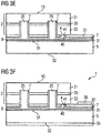
- FIG Figures 3A to 3E An exemplary embodiment of a method for producing a radiation-emitting semiconductor chip is shown in FIG Figures 3A to 3E shown on the basis of intermediate steps shown schematically in sectional view.
- a semiconductor body 2 which has a semiconductor layer sequence with an active region 20, a first semiconductor layer 21 and a second semiconductor layer 22 is provided.
- the semiconductor layer sequence which forms the semiconductor body 2 is preferably deposited epitaxially on a growth substrate 200.
- a second connection layer is formed on the second semiconductor layer 22. This can take place, for example, by means of vapor deposition or sputtering.
- the second connection layer 32 is formed locally structured, for example by means of lithographic techniques, in such a way that the second semiconductor layer 22 is exposed in regions.
- recesses 25 are formed in the semiconductor body 2, which extend through the second semiconductor layer 22 and the active region 20 into the first semiconductor layer 21.
- the semiconductor body 2 is then provided with an insulation layer 7 which covers the second connection layer 32 and in particular the side surfaces of the cutout 41 and the cutouts 25.
- a transition layer 40 is formed in the recess 41.
- the transition layer 40 can, for example be vapor-deposited or sputtered.
- a first connection layer 31 is subsequently deposited on the insulation layer 7, which extends into the recesses 25 and which furthermore directly adjoins the transition layer 40.
- the semiconductor body 2 can then be materially connected to a carrier 5. This can be done by means of a connecting layer 8, which can contain, for example, a solder or an electrically conductive adhesive.
- the semiconductor layer sequence of the semiconductor body 2 can be mechanically stabilized by means of the carrier 5.
- the growth substrate 200 is no longer required for this and can be removed.
- the growth substrate can be removed, for example, mechanically, for example by means of grinding, polishing or lapping and / or chemically, for example by means of wet-chemical or dry-chemical etching. Alternatively or in addition, a laser lift-off process can also be used.
- Material of the semiconductor body 2 is removed in areas in order to expose the second connection layer 32 in areas.
- a first contact 35 and a second contact 36 are deposited on the second main surface 52 of the carrier 5 facing away from the semiconductor body 2 and on the second connection layer 32. This can take place, for example, by means of vapor deposition or sputtering.
- the finished semiconductor chip, which as in the Connection with the Figures 1A and 1B is carried out is in Figure 3F shown.
- the integration of the protective diode 4 in the semiconductor chip 1 can be implemented in the described method without a significant additional expense.
- the electrical contact capability of the semiconductor body 2, in particular of the second semiconductor layer 22, can be locally reduced in a targeted manner prior to the deposition of the transition layer 40. This is preferably done before the first connection layer is deposited.
- the ability to contact can be reduced, for example, by incineration, for example in an O 2 plasma, or sputtering. In this way, the electrical conductivity can be reduced locally in a targeted manner in the region of the recess 41.
- the described method for production was shown only as an example for the production of a semiconductor chip.
- the Semiconductor layer sequence are provided on a wafer, wherein a plurality of semiconductor bodies can emerge from the semiconductor layer sequence by singulation.
- the separation can take place, for example, by means of sawing, breaking, cutting or etching.
Description
Die vorliegende Anmeldung betrifft einen strahlungsemittierenden Halbleiterchip sowie ein Verfahren zur Herstellung eines strahlungsemittierenden Halbleiterchips.The present application relates to a radiation-emitting semiconductor chip and a method for producing a radiation-emitting semiconductor chip.
Elektrostatische Entladung (Electrostatic Discharge) kann bei strahlungsemittierenden Halbleiterchips, beispielsweise bei Leuchtdioden, zur Schädigung bis hin zur Zerstörung führen. Eine solche Schädigung kann durch eine zum Halbleiterchip parallel geschaltete zusätzliche Diode vermieden werden, wobei die Durchlassrichtung der Diode und die Durchlassrichtung des strahlungsemittierenden Halbleiterchips antiparallel zueinander gerichtet sind. Durch diese zusätzliche Diode werden sowohl der Platzbedarf als auch die Herstellungskosten erhöht. Weiterhin kann eine solche zusätzliche Diode zur Absorption von Strahlung führen, wodurch sich die nutzbare optische Leistung des Bauelements verringert. So beschreibt die Offenlegungschrift
Es ist eine Aufgabe, einen strahlungsemittierenden Halbleiterchip anzugeben, der gegenüber elektrostatischer Entladung eine verringerte Empfindlichkeit aufweist. Weiterhin soll ein Verfahren zur Herstellung eines solchen strahlungsemittierenden Halbleiterchips angegeben werden.It is an object to specify a radiation-emitting semiconductor chip which has a reduced sensitivity to electrostatic discharge. Furthermore, a method for producing such a radiation-emitting semiconductor chip is to be specified.
Diese Aufgaben werden durch einen strahlungsemittierenden Halbleiterchip beziehungsweise ein Verfahren zur Herstellung eines strahlungsemittierenden Halbleiterchips gemäß den unabhängigen Patentansprüchen gelöst. Weitere Ausbildungen und Zweckmäßigkeiten sind Gegenstand der abhängigen Patentansprüche.These tasks are achieved by a radiation-emitting semiconductor chip or a method for producing a radiation-emitting semiconductor chip according to FIGS independent claims solved. Further developments and expediencies are the subject of the dependent claims.
Gemäß einer Ausführungsform weist ein strahlungsemittierender Halbleiterchip einen Träger und einen Halbleiterkörper mit einer Halbleiterschichtenfolge auf. Die Halbleiterschichtenfolge weist einen zur Erzeugung von Strahlung vorgesehenen aktiven Bereich, eine erste Halbleiterschicht und eine zweite Halbleiterschicht auf. Der aktive Bereich ist zwischen der ersten Halbleiterschicht und der zweiten Halbleiterschicht angeordnet. Die erste Halbleiterschicht ist auf der dem Träger abgewandten Seite des aktiven Bereichs angeordnet. Der Halbleiterkörper weist zumindest eine Ausnehmung auf, die sich durch den aktiven Bereich hindurch erstreckt. Die erste Halbleiterschicht ist elektrisch leitend mit einer ersten Anschlussschicht verbunden, wobei sich die erste Anschlussschicht in der Ausnehmung von der ersten Halbleiterschicht in Richtung des Trägers erstreckt. Die erste Anschlussschicht ist mit der zweiten Halbleiterschicht über eine Schutzdiode elektrisch verbunden.According to one embodiment, a radiation-emitting semiconductor chip has a carrier and a semiconductor body with a semiconductor layer sequence. The semiconductor layer sequence has an active region provided for generating radiation, a first semiconductor layer and a second semiconductor layer. The active area is arranged between the first semiconductor layer and the second semiconductor layer. The first semiconductor layer is arranged on the side of the active region facing away from the carrier. The semiconductor body has at least one recess which extends through the active region. The first semiconductor layer is connected in an electrically conductive manner to a first connection layer, the first connection layer extending in the recess from the first semiconductor layer in the direction of the carrier. The first connection layer is electrically connected to the second semiconductor layer via a protective diode.
Bei einem Halbleiterchip gemäß dieser Ausführungsform ist die Schutzdiode in den Halbleiterchip integriert. Die Gefahr einer Schädigung des Halbleiterchips, etwa aufgrund von elektrostatischer Entladung ist somit verringert. Auf eine zusätzliche, außerhalb des Halbleiterchips anzuordnende und mit diesem elektrisch leitend zu verbindende Schutzdiode kann verzichtet werden.In the case of a semiconductor chip according to this embodiment, the protective diode is integrated into the semiconductor chip. The risk of damage to the semiconductor chip, for example due to electrostatic discharge, is thus reduced. An additional protective diode to be arranged outside the semiconductor chip and connected to it in an electrically conductive manner can be dispensed with.
Über die Schutzdiode kann insbesondere eine unerwünschte, etwa in Sperrrichtung des Halbleiterchips beziehungsweise eines hierin gebildeten strahlungserzeugenden pn-Übergangs an diesem anliegende, Spannung abfließen. Die Schutzdiode kann insbesondere die Funktion einer ESD (Electrostatic Discharge)-Diode erfüllen, die den Halbleiterchip vor einer Schädigung durch elektrostatische Entladung schützt. Mit anderen Worten können Ladungsträger über einen Strompfad zwischen der ersten Anschlussschicht und der zweiten Halbleiterschicht abfließen. Die Gefahr einer Schädigung des Halbleiterchips kann so verringert werden.In particular, an undesired, for example in the reverse direction of the semiconductor chip or of a radiation-generating pn-junction formed therein, voltage applied to it flow away. The protective diode can in particular fulfill the function of an ESD (Electrostatic Discharge) diode which protects the semiconductor chip from damage by electrostatic discharge. In other words, charge carriers can flow away via a current path between the first connection layer and the second semiconductor layer. The risk of damage to the semiconductor chip can thus be reduced.
Die erste Halbleiterschicht und die zweite Halbleiterschicht des Halbleiterkörpers sind zweckmäßigerweise bezüglich ihres Leitungstyps voneinander verschieden. Beispielsweise kann die erste Halbleiterschicht p-leitend und die zweite Halbleiterschicht n-leitend ausgebildet sein oder umgekehrt.The first semiconductor layer and the second semiconductor layer of the semiconductor body are expediently different from one another with regard to their conductivity type. For example, the first semiconductor layer can be p-conductive and the second semiconductor layer n-conductive, or vice versa.
Eine Diodenstruktur, in der der aktive Bereich ausgebildet ist, ist so auf einfache Weise realisiert.A diode structure in which the active area is formed is thus implemented in a simple manner.
In einer bevorzugten Ausgestaltung ist die Schutzdiode zwischen der ersten Anschlussschicht und der zweiten Halbleiterschicht ausgebildet. Die Schutzdiode kann so auf einfache Weise in einem Strompfad zwischen der ersten Anschlussschicht und der zweiten Halbleiterschicht angeordnet sein.In a preferred configuration, the protective diode is formed between the first connection layer and the second semiconductor layer. The protective diode can thus be arranged in a simple manner in a current path between the first connection layer and the second semiconductor layer.
Weiterhin kann die Schutzdiode außerhalb des Trägers ausgebildet sein. Das Ausbilden der Schutzdiode kann somit weitgehend unabhängig von den Eigenschaften des Trägers, insbesondere der elektrischen Leitfähigkeit oder der elektrischen Kontaktierbarkeit, erfolgen.Furthermore, the protective diode can be formed outside the carrier. The protective diode can thus be formed largely independently of the properties of the carrier, in particular the electrical conductivity or the electrical contactability.
Der Halbleiterchip weist weiterhin bevorzugt einen ersten Kontakt und einen zweiten Kontakt auf, die jeweils für die externe elektrische Kontaktierung des Halbleiterchips vorgesehen sind.The semiconductor chip furthermore preferably has a first contact and a second contact, which are each provided for the external electrical contacting of the semiconductor chip.
Eine zwischen dem ersten Kontakt und dem zweiten Kontakt anliegende Betriebsspannung bewirkt eine Injektion von Ladungsträgern von verschiedenen Seiten des aktiven Bereichs in den aktiven Bereich. Die injizierten Ladungsträger können unter Emission von Strahlung im aktiven Bereich rekombinieren.An operating voltage applied between the first contact and the second contact causes charge carriers to be injected into the active area from different sides of the active area. The injected charge carriers can recombine with the emission of radiation in the active area.
Bezüglich der Durchlassrichtung sind die Diodenstruktur des Halbleiterkörpers und die Schutzdiode zweckmäßigerweise antiparallel zueinander ausgebildet.With regard to the forward direction, the diode structure of the semiconductor body and the protective diode are expediently formed antiparallel to one another.
Durch die Schutzdiode, welche bei der Betriebsspannung des Halbleiterchips in Sperr-Richtung betrieben wird, erfolgt in diesem Fall kein oder zumindest kein wesentlicher Stromfluss. Dagegen kann eine in Sperr-Richtung an der Diodenstruktur anliegende elektrische Spannung, etwa aufgrund elektrostatischer Aufladung, über die Schutzdiode abfließen. So kann der Halbleiterkörper, insbesondere der aktive Bereich, durch die in den Halbleiterchip integrierte Schutzdiode geschützt werden.In this case, there is no or at least no significant current flow through the protective diode, which is operated in the reverse direction when the operating voltage of the semiconductor chip is present. In contrast, an electrical voltage applied to the diode structure in the reverse direction, for example due to electrostatic charging, can flow away via the protective diode. The semiconductor body, in particular the active area, can thus be protected by the protective diode integrated in the semiconductor chip.
In einer bevorzugten Ausgestaltung ist die Schutzdiode als eine Schottky-Diode ausgeführt. Eine Schottky-Diode kann insbesondere mittels eines Metall-Halbleiter-Übergangs gebildet sein, wobei die Strom-Spannungs-Kennlinie des Übergangs von einer Ohmschen Charakteristik abweicht und insbesondere bezüglich der Polarität der anliegenden Spannung asymmetrisch verläuft.In a preferred embodiment, the protective diode is designed as a Schottky diode. A Schottky diode can in particular be formed by means of a metal-semiconductor junction, the current-voltage characteristic of the junction deviating from an ohmic characteristic and, in particular, running asymmetrically with respect to the polarity of the applied voltage.
In einer bevorzugten Ausgestaltung überlappt die Schutzdiode in Aufsicht auf den Halbleiterchip mit dem Halbleiterkörper. Der Halbleiterkörper, insbesondere der aktive Bereich, kann die Schutzdiode in Aufsicht vollständig überdecken. Die Schutzdiode ist somit bei gleicher lateraler Ausdehnung des Halbleiterkörpers in den Halbleiterchip integrierbar. Weiterhin ist so die Schutzdiode unter Beibehaltung der für die Strahlungserzeugung nutzbaren Fläche des aktiven Bereichs in den Halbleiterchip integrierbar.In a preferred embodiment, the protective diode overlaps with the semiconductor body in a plan view of the semiconductor chip. The semiconductor body, in particular the active area, can completely cover the protective diode in plan view. The protective diode can thus be integrated into the semiconductor chip with the same lateral extent of the semiconductor body. Furthermore, the protective diode can thus be integrated into the semiconductor chip while maintaining the area of the active region that can be used for generating radiation.
Unter einer lateralen Richtung wird eine Richtung verstanden, die entlang einer Haupterstreckungsebene der Halbleiterschichten des Halbleiterkörpers verläuft.A lateral direction is understood to mean a direction which runs along a main plane of extent of the semiconductor layers of the semiconductor body.
In einer bevorzugten Weiterbildung ist die Schutzdiode mittels der zweiten Halbleiterschicht gebildet. Die zweite Halbleiterschicht kann also sowohl für die Injektion von Ladungsträgern in den aktiven Bereich als auch für das Ausbilden der Schutzdiode vorgesehen sein. Auf einen separaten, elektrisch vom aktiven Bereich isolierten, Halbleiterbereich für das Ausbilden der Schottky-Diode kann so verzichtet werden. Mit anderen Worten kann die Schutzdiode, insbesondere in Form einer Schottky-Diode, bei gleicher lateraler Ausdehnung des Halbleiterchips in den Halbleiterchip integriert sein, ohne dass die für die Strahlungserzeugung maßgebliche Fläche des aktiven Bereichs verringert wird. Die Integration der Schutzdiode in den Halbleiterchip kann somit ohne eine Beeinträchtigung der optoelektronischen Eigenschaften des Halbleiterchips erfolgen.In a preferred development, the protective diode is formed by means of the second semiconductor layer. The second semiconductor layer can therefore be provided both for the injection of charge carriers into the active region and for the formation of the protective diode. A separate semiconductor region, which is electrically isolated from the active region, for forming the Schottky diode can thus be dispensed with. In other words, the protective diode, in particular in the form of a Schottky diode, can be integrated into the semiconductor chip with the same lateral extent of the semiconductor chip, without reducing the area of the active region that is decisive for generating radiation. The protection diode can thus be integrated into the semiconductor chip without impairing the optoelectronic properties of the semiconductor chip.
In einer bevorzugten Ausgestaltung verläuft die erste Anschlussschicht zumindest bereichsweise zwischen dem Träger und der zweiten Halbleiterschicht. Mittels der ersten Anschlussschicht ist die erste Halbleiterschicht von der dem Träger zugewandten Seite des aktiven Bereichs her elektrisch kontaktierbar.In a preferred embodiment, the first connection layer runs at least in some areas between the carrier and the second semiconductor layer. By means of the first connection layer, electrical contact can be made with the first semiconductor layer from the side of the active region facing the carrier.
In einer bevorzugten Weiterbildung ist zumindest bereichsweise zwischen der ersten Anschlussschicht und der zweiten Halbleiterschicht eine zweite Anschlussschicht angeordnet. Die zweite Anschlussschicht ist elektrisch leitend mit der zweiten Halbleiterschicht verbunden und grenzt weiterhin bevorzugt unmittelbar an die zweite Halbleiterschicht an.In a preferred development, a second connection layer is arranged at least in regions between the first connection layer and the second semiconductor layer. The second connection layer is connected in an electrically conductive manner to the second semiconductor layer and furthermore preferably directly adjoins the second semiconductor layer.
Zweckmäßigerweise sind die erste Anschlussschicht und die zweite Anschlussschicht jeweils über den ersten beziehungsweise zweiten Kontakt extern elektrisch kontaktierbar. Der erste und/oder der zweite Kontakt können jeweils mittels einer Kontaktschicht gebildet sein, die, vorzugsweise unmittelbar, auf der ersten beziehungsweise zweiten Anschlussschicht angeordnet ist. Davon abweichend kann die erste Anschlussschicht den ersten Kontakt und/oder die zweite Anschlussschicht den zweiten Kontakt bilden. In diesem Fall kann also zumindest auf eine separate, zusätzlich zu den Anschlussschichten vorgesehene und den ersten beziehungsweise zweiten Kontakt bildende, Kontaktschicht verzichtet werden.Expediently, the first connection layer and the second connection layer can each be electrically contacted externally via the first and second contact, respectively. The first and / or the second contact can each be formed by means of a contact layer which is arranged, preferably directly, on the first or second connection layer. In a departure from this, the first connection layer can form the first contact and / or the second connection layer can form the second contact. In this case, at least one separate contact layer, which is provided in addition to the connection layers and forms the first or second contact, can be dispensed with.
Die erste Anschlussschicht und/oder die zweite Anschlussschicht enthalten vorzugsweise jeweils ein Metall, beispielsweise Ti, Pt, Ni, Au, Ag, Al, Rh, Pd, Pt oder W oder eine metallische Legierung mit zumindest einem der genannten Materialien. Die erste und/oder die zweite Anschlussschicht sind vorzugsweise außerhalb des Halbleiterkörpers angeordnet und mittels eines nicht-epitaktischen Verfahrens, etwa Aufdampfens oder Sputterns, hergestellt.The first connection layer and / or the second connection layer preferably each contain a metal, for example Ti, Pt, Ni, Au, Ag, Al, Rh, Pd, Pt or W or a metallic alloy with at least one of the materials mentioned. The first and / or the second connection layer are preferably arranged outside the semiconductor body and fabricated by a non-epitaxial process such as vapor deposition or sputtering.
In einer Ausgestaltungsvariante ist die Schutzdiode mittels einer Übergangsschicht gebildet, die auf der zweiten Halbleiterschicht angeordnet ist und weiterhin bevorzugt an die zweite Halbleiterschicht angrenzt. Die Übergangsschicht und die zweite Anschlussschicht sind zweckmäßigerweise in lateraler Richtung voneinander beabstandet. Ein direkter elektrischer Kontakt zwischen der Übergangsschicht und der zweiten Anschlussschicht ist so auf einfache Weise vermeidbar.In one embodiment variant, the protective diode is formed by means of a transition layer which is arranged on the second semiconductor layer and furthermore preferably adjoins the second semiconductor layer. The transition layer and the second connection layer are expediently spaced apart from one another in the lateral direction. A direct electrical contact between the transition layer and the second connection layer can thus be avoided in a simple manner.
Weiterhin bevorzugt ist zwischen der Übergangsschicht und der zweiten Anschlussschicht eine Isolationsschicht ausgebildet. Die Gefahr eines elektrischen Kurzschlusses zwischen der Übergangsschicht und der zweiten Anschlussschicht kann so weitergehend verringert werden.Furthermore, an insulation layer is preferably formed between the transition layer and the second connection layer. The risk of an electrical short circuit between the transition layer and the second connection layer can thus be further reduced.
Die Übergangsschicht ist bezüglich des Materials vorzugsweise derart gewählt, dass ein Schottky-Übergang, also ein Metall-Halbleiter-Übergang mit asymmetrischer Strom-Spannungs-Charakteristik, zur zweiten Halbleiterschicht vereinfacht realisierbar ist.With regard to the material, the transition layer is preferably selected in such a way that a Schottky transition, that is to say a metal-semiconductor transition with asymmetrical current-voltage characteristics, to the second semiconductor layer can be implemented in a simplified manner.
In einer alternativen Ausgestaltungsvariante ist die Schutzdiode mittels der ersten Anschlussschicht gebildet, wobei die erste Anschlussschicht vorzugsweise an die zweite Halbleiterschicht angrenzt. In diesem Fall grenzt die erste Anschlussschicht also an die erste Halbleiterschicht und an die zweite Halbleiterschicht an, wobei zwischen der ersten Anschlussschicht und der ersten Kontaktschicht ein Ohm'scher oder zumindest näherungsweise Ohm'scher Kontakt und zwischen der ersten Anschlussschicht und der zweiten Kontaktschicht ein Schottky-Kontakt gebildet ist.In an alternative configuration variant, the protective diode is formed by means of the first connection layer, the first connection layer preferably adjoining the second semiconductor layer. In this case, the first connection layer adjoins the first semiconductor layer and the second semiconductor layer, with an ohmic or at least approximately ohmic contact between the first connection layer and the first contact layer and between a Schottky contact is formed between the first connection layer and the second contact layer.
Das Material für die an die zweite Halbleiterschicht angrenzende Schicht, also die Übergangsschicht oder die erste Anschlussschicht, ist vorzugsweise derart gewählt, dass ein Schottky-Kontakt zur zweiten Halbleiterschicht vereinfacht ausgebildet werden kann.The material for the layer adjoining the second semiconductor layer, that is to say the transition layer or the first connection layer, is preferably selected such that a Schottky contact to the second semiconductor layer can be formed in a simplified manner.
In einer bevorzugten Weiterbildung weist die zweite Halbleiterschicht zumindest bereichsweise, insbesondere im Bereich der Schutzdiode, eine lokal gezielt verringerte Kontaktfähigkeit auf. Ein solcher Bereich verringerter Kontaktfähigkeit ist beispielsweise mittels Veraschens, etwa in einem Sauerstoffhaltigen Plasma, oder Sputterns herstellbar. Auf diese Weise kann die elektrische Leitfähigkeit der zweiten Halbleiterschicht gezielt verringert werden.In a preferred development, the second semiconductor layer has, at least in some areas, in particular in the area of the protective diode, a locally targeted reduced contact capability. Such an area of reduced contactability can be produced, for example, by ashing, for example in an oxygen-containing plasma, or by sputtering. In this way, the electrical conductivity of the second semiconductor layer can be reduced in a targeted manner.
So kann zwischen der zweiten Halbleiterschicht und der Übergangsschicht beziehungsweise der ersten Anschlussschicht ein Kontakt mit einer hinreichend hohen Potenzial-Barriere vereinfacht realisiert werden. Die Freiheit bezüglich des Materials der an die zweite Halbleiterschicht angrenzenden Schicht, also der Übergangsschicht oder der ersten Anschlussschicht, ist so weitergehend erhöht. Insbesondere kann die Schicht ein Material enthalten oder aus einem Material bestehen, das für die im aktiven Bereich erzeugte Strahlung eine hohe Reflektivität aufweist. Für Strahlung im sichtbaren oder im ultravioletten Spektralbereich zeichnen sich beispielsweise Silber oder Aluminium durch eine hohe Reflektivität auf.In this way, a contact with a sufficiently high potential barrier can be implemented in a simplified manner between the second semiconductor layer and the transition layer or the first connection layer. The freedom with regard to the material of the layer adjoining the second semiconductor layer, that is to say the transition layer or the first connection layer, is thus increased further. In particular, the layer can contain a material or consist of a material which has a high reflectivity for the radiation generated in the active region. For radiation in the visible or in the ultraviolet spectral range, for example, silver or aluminum are characterized by a high reflectivity.
In einer Ausgestaltungsvariante sind der erste Kontakt und der zweite Kontakt auf unterschiedlichen Seiten des Trägers ausgebildet. In diesem Fall ist der Träger vorzugsweise elektrisch leitfähig ausgebildet.In one embodiment, the first contact and the second contact are formed on different sides of the carrier. In this case, the carrier is preferably designed to be electrically conductive.
In einer alternativen Ausgestaltungsvariante sind der erste Kontakt und der zweite Kontakt auf der dem Halbleiterkörper zugewandten Seite des Trägers angeordnet. In diesem Fall kann der Träger unabhängig von seiner elektrischen Leitfähigkeit gewählt werden und insbesondere elektrisch isolierend ausgebildet sein.In an alternative configuration variant, the first contact and the second contact are arranged on the side of the carrier facing the semiconductor body. In this case, the carrier can be selected independently of its electrical conductivity and, in particular, can be designed to be electrically insulating.
Als elektrisch leitfähiges Trägermaterial eignet sich beispielsweise ein, vorzugsweise dotiertes, Halbleitermaterial. Zum Beispiel kann der Träger Silizium, Germanium, Galliumarsenid oder Galliumnitrid enthalten oder aus einem solchen Material bestehen.For example, a preferably doped semiconductor material is suitable as the electrically conductive carrier material. For example, the carrier can contain silicon, germanium, gallium arsenide or gallium nitride or consist of such a material.
Weiterhin eignet sich als Trägermaterial beispielsweise eine Keramik, etwa Aluminiumnitrid oder Bornitrid. Ein solcher Träger kann elektrisch isolierend ausgebildet sein.A ceramic, for example aluminum nitride or boron nitride, is also suitable as a carrier material. Such a carrier can be designed to be electrically insulating.
Der Halbleiterkörper ist vorzugsweise stoffschlüssig mit dem Träger verbunden. Der Träger ist insbesondere von einem Aufwachssubstrat für die Halbleiterschichtenfolge des Halbleiterkörpers verschieden. Der Träger stabilisiert vorzugsweise die Halbleiterschichtenfolge des Halbleiterkörpers mechanisch. Das Aufwachssubstrat des Halbleiterkörpers ist hierfür nicht erforderlich und kann entfernt sein.The semiconductor body is preferably materially connected to the carrier. The carrier is in particular different from a growth substrate for the semiconductor layer sequence of the semiconductor body. The carrier preferably mechanically stabilizes the semiconductor layer sequence of the semiconductor body. The growth substrate of the semiconductor body is not required for this and can be removed.
Bei einer stoffschlüssigen Verbindung werden die Verbindungspartner, die bevorzugt vorgefertigt sind, mittels atomarer und/oder molekularer Kräfte zusammengehalten. Eine stoffschlüssige Verbindung kann beispielsweise mittels einer Verbindungsschicht, etwa einer Klebeschicht oder einer Lotschicht, erzielt werden. In der Regel geht eine Trennung der Verbindung mit der Zerstörung der Verbindungsschicht und/oder zumindest eines der Verbindungspartner einher.In the case of a material connection, the connection partners, which are preferably prefabricated, are connected by means of held together by atomic and / or molecular forces. A material connection can be achieved, for example, by means of a connection layer, for example an adhesive layer or a solder layer. As a rule, a disconnection is accompanied by the destruction of the connection layer and / or at least one of the connection partners.
In einer bevorzugten Weiterbildung ist das Aufwachssubstrat für die Halbleiterschichtenfolge des Halbleiterkörpers zumindest bereichsweise entfernt. Insbesondere kann das Aufwachssubstrat vollflächig oder bereichsweise gedünnt oder vollflächig oder bereichsweise entfernt sein.In a preferred development, the growth substrate for the semiconductor layer sequence of the semiconductor body is removed at least in some areas. In particular, the growth substrate can be thinned over the entire area or in areas or removed over the entire area or in areas.
Ein Halbleiterchip, bei dem das Aufwachssubstrat entfernt ist, wird auch als Dünnfilm-Halbleiterchip bezeichnet.A semiconductor chip from which the growth substrate has been removed is also referred to as a thin-film semiconductor chip.
Ein Dünnfilm-Halbleiterchip, etwa ein Dünnfilm-Leuchtdioden-Chip, kann sich weiterhin im Rahmen der vorliegenden Anmeldung durch mindestens eines der folgenden charakteristischen Merkmale auszeichnen:
- an einer zu einem Trägerelement hin gewandten ersten Hauptfläche eines Halbleiterkörpers, der eine Halbleiterschichtenfolge mit einem aktiven Bereich umfasst, insbesondere einer Epitaxieschichtenfolge, ist eine Spiegelschicht aufgebracht oder, etwa als Braggspiegel in der Halbleiterschichtenfolge integriert, ausgebildet, die zumindest einen Teil der in der Halbleiterschichtenfolge erzeugten Strahlung in diese zurückreflektiert;
- die Halbleiterschichtenfolge weist eine Dicke im Bereich von 20pm oder weniger, insbesondere
im Bereich von 10 µm auf; und/oder - die Halbleiterschichtenfolge enthält mindestens eine Halbleiterschicht mit zumindest einer Fläche, die eine Durchmischungsstruktur aufweist, die im Idealfall zu einer annähernd ergodischen Verteilung des Lichtes in der Halbleiterschichtenfolge führt, d.h. sie weist ein möglichst ergodisch stochastisches Streuverhalten auf. Ein Grundprinzip eines Dünnfilm-Leuchtdiodenchips ist beispielsweise in
I. Schnitzer et al., Appl. Phys. Lett. 63 (16), 18. Oktober 1993, 2174 - 2176
- On a first main surface of a semiconductor body, facing a carrier element, which comprises a semiconductor layer sequence with an active region, in particular an epitaxial layer sequence, a mirror layer is applied or, for example, integrated as a Bragg mirror in the semiconductor layer sequence, which is at least part of that produced in the semiconductor layer sequence Radiation reflected back into it;
- the semiconductor layer sequence has a thickness in the range of 20 μm or less, in particular in the range of 10 μm; and or
- The semiconductor layer sequence contains at least one semiconductor layer with at least one surface which has a mixing structure which, in the ideal case, leads to an approximately ergodic distribution of the light in the semiconductor layer sequence, ie it has a scattering behavior that is as ergodic as possible. A basic principle of a thin-film light-emitting diode chip is for example in
I. Schnitzer et al., Appl. Phys. Lett. 63 (16), October 18, 1993, 2174-2176
Die Halbleiterschichtenfolge des Halbleiterkörpers ist vorzugsweise epitaktisch, etwa mittels MOVPE oder MBE, abgeschieden.The semiconductor layer sequence of the semiconductor body is preferably deposited epitaxially, for example by means of MOVPE or MBE.
Weiterhin bevorzugt enthält der Halbleiterkörper, insbesondere der aktive Bereich, ein III-V-Halbleitermaterial. Mit III-V-Halbleitermaterialen können bei der Strahlungserzeugung hohe interne Quanteneffizienzen erreicht werden.Furthermore, the semiconductor body, in particular the active region, preferably contains a III-V semiconductor material. With III-V semiconductor materials, high internal quantum efficiencies can be achieved when generating radiation.
Der beschriebene Aufbau ist generell für optoelektronische Halbleiterchips geeignet, die zur Strahlungserzeugung und/oder zur Detektion von Strahlung vorgesehen sind. Insbesondere kann der Halbleiterchip zur Erzeugung von inkohärenter, teilkohärenter oder kohärenter Strahlung vorgesehen sein. Zur Erzeugung inkohärenter Strahlung eignet sich beispielsweise ein Aufbau gemäß einem LED-Chip, für die Erzeugung teilkohärenter Strahlung ein Aufbau gemäß einem RCLED-Chip (Resonant Cavity Light Emitting Diode). Kohärente Strahlung kann beispielsweise mittels eines Halbleiterlaser-Chips erzeugt werden, der insbesondere als
kantenemittierender Laser oder als oberflächenemittierender Laser, etwa als VCSEL (vertical cavity surface emitting laser) oder als VECSEL (vertical external cavity surface emitting laser) ausgeführt sein kann.The structure described is generally suitable for optoelectronic semiconductor chips which are provided for generating radiation and / or for detecting radiation. In particular, the semiconductor chip can be provided for generating incoherent, partially coherent or coherent radiation. A structure based on an LED chip is suitable for generating incoherent radiation, for example, and a structure based on an RCLED chip (Resonant Cavity Light Emitting Diode) is suitable for generating partially coherent radiation. Coherent Radiation can be generated, for example, by means of a semiconductor laser chip, which in particular is used as a
edge-emitting laser or as a surface-emitting laser, for example as a VCSEL (vertical cavity surface emitting laser) or as a VECSEL (vertical external cavity surface emitting laser).
Bei einem Verfahren zur Herstellung eines
strahlungsemittierenden Halbleiterchips wird gemäß einer Ausführungsform ein Halbleiterkörper mit einer Halbleiterschichtenfolge bereitgestellt, die einen zur Erzeugung von Strahlung vorgesehenen aktiven Bereich, eine erste Halbleiterschicht und eine zweite Halbleiterschicht aufweist. Im Halbleiterkörper wird eine Ausnehmung ausgebildet, die sich durch den aktiven Bereich hindurch in die erste Halbleiterschicht hinein erstreckt. Auf dem Halbleiterkörper wird eine erste Anschlussschicht ausgebildet, wobei sich die erste Anschlussschicht in die Ausnehmung hinein erstreckt. Die erste Anschlussschicht ist mit der zweiten Halbleiterschicht über eine Schutzdiode elektrisch verbunden. Der Halbleiterchip wird fertig gestellt.In a method of making a
According to one embodiment, radiation-emitting semiconductor chips are provided with a semiconductor body with a semiconductor layer sequence which has an active region provided for generating radiation, a first semiconductor layer and a second semiconductor layer. A recess is formed in the semiconductor body which extends through the active region into the first semiconductor layer. A first connection layer is formed on the semiconductor body, the first connection layer extending into the recess. The first connection layer is electrically connected to the second semiconductor layer via a protective diode. The semiconductor chip is completed.
Die Verfahrensschritte müssen hierbei nicht notwendigerweise in der Reihenfolge der obigen Aufzählung durchgeführt werden.The process steps do not necessarily have to be carried out in the order of the above list.
Ein Verfahren, bei dem eine Schutzdiode in den Halbleiterchip integriert werden kann, ist so auf einfache und kostengünstige Weise realisiert. Mit diesem Verfahren können eine Vielzahl von Halbleiterchips gleichzeitig, insbesondere nebeneinander auf einem Wafer, hergestellt werden. Bei diesem Verfahren können durch Vereinzelung Halbleiterchips hervorgehen, in die bereits eine Schutzdiode integriert ist.A method in which a protective diode can be integrated into the semiconductor chip is thus implemented in a simple and inexpensive manner. With this method, a large number of semiconductor chips can be produced simultaneously, in particular next to one another on a wafer. With this method, semiconductor chips can be produced through isolation in which a protective diode is already integrated.
Die Integration der Schutzdiode kann somit auf Wafer-Ebene, also noch vor Vereinzelung der Halbleiterchips erfolgen.The protection diode can thus be integrated at the wafer level, that is, before the semiconductor chips are singulated.
In einer bevorzugten Ausgestaltung wird vor dem Ausbilden der ersten Anschlussschicht auf der zweiten Halbleiterschicht eine Übergangsschicht ausgebildet, die an die zweite Halbleiterschicht angrenzt. Insbesondere kann mittels der Übergangsschicht eine Schottky-Diode ausgebildet werden.In a preferred configuration, before the first connection layer is formed on the second semiconductor layer, a transition layer is formed which adjoins the second semiconductor layer. In particular, a Schottky diode can be formed by means of the transition layer.
In einer bevorzugten Weiterbildung wird die elektrische Kontaktfähigkeit der zweiten Halbleiterschicht gezielt lokal verringert. Dies kann insbesondere vor dem Abscheiden der Übergangsschicht erfolgen.In a preferred development, the electrical contactability of the second semiconductor layer is specifically reduced locally. This can take place in particular before the transition layer is deposited.
Insbesondere kann die elektrische Kontaktfähigkeit mittels Veraschens und/oder mittels Sputterns verringert werden.In particular, the electrical contact capability can be reduced by ashing and / or by sputtering.
In einer weiteren bevorzugten Ausgestaltung wird die zweite Anschlussschicht mittels bereichsweisen Entfernens des Halbleiterkörpers freigelegt. In dem freigelegten Bereich der zweiten Anschlussschicht kann ein Kontakt ausgebildet werden, der zur elektrischen Kontaktierung des Halbleiterchips vorgesehen ist.In a further preferred configuration, the second connection layer is exposed by removing the semiconductor body in regions. In the exposed region of the second connection layer, a contact can be formed which is provided for making electrical contact with the semiconductor chip.
Das beschriebene Verfahren ist zur Herstellung eines weiter oben beschriebenen strahlungsemittierenden Halbleiterchips besonders geeignet. Die im Zusammenhang mit dem Verfahren beschriebenen Merkmale können daher auch für den Halbleiterchip herangezogen werden und umgekehrt.The method described is particularly suitable for producing a radiation-emitting semiconductor chip described above. The features described in connection with the method can therefore also be used for the semiconductor chip and vice versa.
Weitere Merkmale, Ausgestaltungen und Zweckmäßigkeiten ergeben sich aus der folgenden Beschreibung der Ausführungsbeispiele in Verbindung mit den Figuren.Further features, configurations and expediencies emerge from the following description of the exemplary embodiments in conjunction with the figures.
Es zeigen:
- Die Figuren 1A und 1B
- ein Ausführungsbeispiel für einen strahlungsemittierenden Halbleiterchip in schematischer Aufsicht (
Figur 1B ) und zugehöriger Schnittansicht (Figur 1A ); Figur 2- eine schematische Darstellung der Strompfade in einem Halbleiterchip gemäß dem in den
Figuren 1A und 1B dargestellten ersten Ausführungsbeispiel; und - die Figuren 3A bis 3F
- ein Ausführungsbeispiel für ein Verfahren zur Herstellung eines strahlungsemittierenden Halbleiterchips anhand von jeweils in schematischer Schnittansicht dargestellten Zwischenschritten.
- Figures 1A and 1B
- an embodiment of a radiation-emitting semiconductor chip in a schematic plan view (
Figure 1B ) and associated sectional view (Figure 1A ); - Figure 2
- a schematic representation of the current paths in a semiconductor chip according to the in FIG
Figures 1A and 1B illustrated first embodiment; and - Figures 3A to 3F
- an exemplary embodiment of a method for producing a radiation-emitting semiconductor chip on the basis of intermediate steps illustrated in each case in a schematic sectional view.
Gleiche, gleichartige oder gleich wirkende Elemente sind in den Figuren mit gleichen Bezugszeichen versehen.Identical, identical or identically acting elements are provided with the same reference symbols in the figures.
Die Figuren sind jeweils schematische Darstellungen und daher nicht unbedingt maßstabsgetreu. Vielmehr können vergleichsweise kleine Elemente und insbesondere Schichtdicken zur Verdeutlichung übertrieben groß dargestellt sein.The figures are each schematic representations and are therefore not necessarily true to scale. Rather, comparatively small elements and in particular layer thicknesses can be shown exaggerated for clarity.
Ein erstes Ausführungsbeispiel für einen
strahlungsemittierenden Halbleiterchip ist schematisch anhand einer Aufsicht in
radiation-emitting semiconductor chip is schematically based on a plan in
Der strahlungsemittierende Halbleiterchip 1 weist einen Halbleiterkörper 2 auf, der mittels einer Verbindungsschicht 8 an einem Träger 5 befestigt ist.The radiation-emitting semiconductor chip 1 has a
Die Halbleiterschichtenfolge, die den Halbleiterkörper 2 bildet, ist vorzugsweise epitaktisch, etwa mittels MOVPE oder MBE, hergestellt.The semiconductor layer sequence which forms the
Der Halbleiterkörper weist einen zur Erzeugung von Strahlung vorgesehenen aktiven Bereich 20 auf, der zwischen einer ersten Halbleiterschicht 21 und einer zweiten Halbleiterschicht 22 angeordnet ist. Die erste Halbleiterschicht 21 und die zweite Halbleiterschicht 22 sind bezüglich ihres Leitungstyps voneinander verschieden. Beispielsweise kann die zweite Halbleiterschicht 22 p-leitend und die erste Halbleiterschicht 21 n-leitend ausgebildet sein oder umgekehrt.The semiconductor body has an
Der Halbleiterkörper 2 weist eine Mehrzahl von Ausnehmungen 25 auf, die sich vom Träger 5 her durch die zweite Halbleiterschicht 22 und den aktiven Bereich 20 in die erste Halbleiterschicht 21 hinein erstrecken.The
Die Ausnehmungen 25 sind exemplarisch in Aufsicht jeweils kreisförmig ausgebildet und matrixförmig angeordnet. Die Ausnehmungen können aber auch eine andere Grundform, etwa eine mehreckige, beispielsweise rechteckige oder quadratische Grundform aufweisen. Die Ausnehmungen sind zweckmäßigerweise derart angeordnet, dass Ladungsträger in lateraler Richtung gleichmäßig von der ersten Halbleiterschicht 21 in den aktiven Bereich injiziert werden können. Insbesondere bei einer hinreichend hohen elektrischen Leitfähigkeit der ersten Halbleiterschicht 21 in lateraler Richtung kann von dem beschriebenen Ausführungsbeispiel abweichend auch nur eine einzelne Ausnehmung vorgesehen sein.The
Der Träger 5 weist eine erste Hauptfläche 51 und eine weitere Hauptfläche 52 auf. Die erste Hauptfläche 51 ist dem Halbleiterkörper 2 zugewandt und vorzugsweise eben ausgeführt. Eine stoffschlüssige Befestigung des Halbleiterkörpers an dem Träger ist so vereinfacht realisierbar.The
Als Trägermaterial eignet sich beispielsweise ein, vorzugsweise dotiertes, Halbleitermaterial. Zum Beispiel kann der Träger Silizium, Germanium, Galliumarsenid oder Galliumnitrid enthalten oder aus einem solchen Material bestehen. Alternativ oder ergänzend kann der Träger eine Keramik, etwa AlN oder BN enthalten.For example, a preferably doped semiconductor material is suitable as the carrier material. For example, the carrier can contain silicon, germanium, gallium arsenide or gallium nitride or consist of such a material. As an alternative or in addition, the carrier can contain a ceramic, for example AlN or BN.
Zwischen dem Halbleiterkörper 2 und dem Träger 5 ist eine erste Anschlussschicht 31 ausgebildet, die sich in die Ausnehmungen 25 hinein erstreckt. Mittels der ersten Anschlussschicht ist die erste Halbleiterschicht 21 von der dem Träger zugewandten Seite des aktiven Bereichs 20 her elektrisch kontaktierbar.A
Eine dem Träger 5 abgewandte Strahlungsaustrittsfläche 10 des Halbleiterkörpers 2 kann so frei von einem externen elektrischen Kontakt ausgebildet werden. Die Gefahr einer Abschattung der Strahlungsaustrittsfläche durch einen Kontakt, der für die im aktiven Bereich erzeugte Strahlung undurchlässig ist, kann vermieden werden.A
Die Seitenflächen der Ausnehmungen 25 sind mit einer Isolationsschicht 7 versehen. Ein elektrischer Kurzschluss des aktiven Bereichs 20 durch die erste Anschlussschicht 31 kann auf einfache Weise verhindert werden.The side surfaces of the
Die Isolationsschicht 7 kann beispielsweise ein Nitrid, etwa Siliziumnitrid, ein Oxid, etwa Siliziumoxid oder Titanoxid, oder ein Oxinitrid, etwa Siliziumoxinitrid, enthalten oder aus einem solchen Material bestehen.The
Die zweite Halbleiterschicht 22 ist mit einer zweiten Anschlussschicht 32 elektrisch leitend verbunden. Die zweite Anschlussschicht verläuft bereichsweise zwischen der ersten Anschlussschicht 31 und der zweiten Halbleiterschicht 22.The
Weiterhin weist der Halbleiterchip 1 einen ersten Kontakt 35 und einen zweiten Kontakt 36 auf. Die Kontakte sind zur externen elektrischen Kontaktierung des Halbleiterchips vorgesehen und dienen der Injektion von Ladungsträgern von verschiedenen Seiten des aktiven Bereichs 20 in den aktiven Bereich, so dass die injizierten Ladungsträger im aktiven Bereich unter Emission von Strahlung rekombinieren können.Furthermore, the semiconductor chip 1 has a
Mittels der ersten Anschlussschicht 31 und der zweiten Anschlussschicht 32 ist der Halbleiterkörper von derselben Seite des Halbleiterkörpers her derart elektrisch kontaktierbar, dass Ladungsträger im Betrieb in den aktiven Bereich 20 verschiedenen Seiten injiziert werden können. Auf diese Weise ist vereinfacht ein Halbleiterchip realisierbar, dessen Strahlungsaustrittsfläche frei von externen elektrischen Kontakten ist.By means of the
Der erste Kontakt 35 ist über den Träger 5 und die Verbindungsschicht 8 mit der ersten Anschlussschicht 31 elektrisch leitend verbunden. Der zweite Kontakt 36 ist auf der zweiten Anschlussschicht 32 angeordnet und mit dieser elektrisch leitend verbunden.The
Zwischen der ersten Anschlussschicht 31 und der zweiten Halbleiterschicht 22 ist eine Schutzdiode 4 ausgebildet.A
Die Schutzdiode 4 ist mittels einer Übergangsschicht 40 gebildet, die sich von der zweiten Halbleiterschicht 22 in vertikaler Richtung bis zur ersten Anschlussschicht 31 erstreckt. Die Schutzdiode 4 ist als eine Schottky-Diode ausgeführt, bei der die Übergangsschicht 40 und die zweite Halbleiterschicht 22 einen Metall-Halbleiter-Übergang bilden.The
In Aufsicht auf den Halbleiterchip 1 überdeckt der Halbleiterkörper 2, insbesondere der aktive Bereich 20, die Schutzdiode 4 vollständig. Die Schutzdiode ist also derart in den Halbleiterkörper integriert, dass sowohl die für die Strahlungserzeugung nutzbare Fläche als auch die laterale Ausdehnung des Halbleiterchips beibehalten werden kann.In a plan view of the semiconductor chip 1, the
Bezüglich des Materials ist die Übergangsschicht vorzugsweise derart gewählt, dass eine im Betrieb des Halbleiterchips 1 in Vorwärtsrichtung anliegende Betriebsspannung zu keinem oder zumindest keinen wesentlichen Stromfluss zwischen der ersten Anschlussschicht 31 und der zweiten Halbleiterschicht 22 führt. Die Strompfade innerhalb des Halbleiterchips werden im Zusammenhang mit
Bei einem Halbleiterkörper, der Inx Gay Al1-x-y N mit 0 ≤ x ≤ 1, 0 ≤ y ≤ 1 und x + y ≤ 1, insbesondere mit x ≠ 1, y ≠ 1, x ≠ 0 und/oder y ≠ 0 enthält, eignet sich beispielsweise eine Übergangsschicht, die TiWN enthält oder aus einer solchen Materialzusammensetzung besteht.In the case of a semiconductor body, the In x Ga y Al 1-xy N with 0 x 1, 0 y 1 and x + y 1, in particular with x ≠ 1, y ≠ 1, x ≠ 0 and / or y Contains ≠ 0, for example, a transition layer that contains TiWN or consists of such a material composition is suitable.
Alternativ oder ergänzend kann die Übergangsschicht 40 als eine hochreflektive Metallschicht ausgebildet sein. Beispielsweise weisen Silber und Aluminium eine hohe Reflektivität im sichtbaren und ultravioletten Spektralbereich auf. Im aktiven Bereich erzeugte und in Richtung des Trägers 5 abgestrahlte Strahlung kann so auf effiziente Weise in Richtung der Strahlungsaustrittsfläche umgelenkt werden.As an alternative or in addition, the
In der zweiten Anschlussschicht 32 ist eine Aussparung 41 ausgebildet. Durch diese Aussparung hindurch erstreckt sich die Übergangsschicht 40. Die Seitenflächen der Aussparung 41 sind mit der Isolationsschicht 7 bedeckt. Ein elektrischer Kurzschluss zwischen der Übergangsschicht 40 und der zweiten Anschlussschicht 32 kann so vermieden werden.A
Die Anschlussschichten 31 und 32 enthalten vorzugsweise jeweils ein Metall, etwa Ti, Pt, Ni, Au, Ag, Al, Rh, Pd, Pt oder W oder eine metallische Legierung mit zumindest einem der genannten Metalle.The connection layers 31 and 32 preferably each contain a metal, for example Ti, Pt, Ni, Au, Ag, Al, Rh, Pd, Pt or W or a metallic alloy with at least one of the metals mentioned.
Die erste Anschlussschicht 35 und/oder die zweite 36 Anschlussschicht können auch mehrschichtig ausgeführt sein.The
Weiterhin können die erste Anschlussschicht 31 und/oder die zweite Anschlussschicht 32 auch ein TCO (Transparent conductive oxide)-Material, etwa Zinkoxid, Indiumoxid oder Indiumzinnoxid (ITO) enthalten.Furthermore, the
Der Halbleiterkörper 2, insbesondere der aktive Bereich 20, enthält vorzugsweise ein III-V-Halbleitermaterial.The
III-V-Halbleitermaterialien sind zur Strahlungserzeugung im ultravioletten (Inx Gay Al1-x-y N) über den sichtbaren (Inx Gay Al1-x-y N, insbesondere für blaue bis grüne Strahlung, oder Inx Gay Al1-x-y P, insbesondere für gelbe bis rote Strahlung) bis in den infraroten (Inx Gay Al1-x-y As) Spektralbereich besonders geeignet. Hierbei gilt jeweils 0 ≤ x ≤ 1, 0 ≤ y ≤ 1 und x + y ≤ 1, insbesondere mit x ≠ 1, y ≠ 1, x ≠ 0 und/oder y ≠ 0. Mit III-V-Halbleitermaterialien, insbesondere aus den genannten Materialsystemen, können weiterhin bei der Strahlungserzeugung hohe interne Quanteneffizienzen erzielt werden.III-V semiconductor materials are used to generate radiation in the ultraviolet (In x Ga y Al 1-xy N) over the visible (In x Ga y Al 1-xy N, especially for blue to green radiation, or In x Ga y Al 1- xy P, especially for yellow to red radiation) into the infrared (In x Ga y Al 1-xy As) spectral range is particularly suitable. 0 x 1, 0 y 1 and x + y 1, in particular with x ≠ 1, y ≠ 1, x ≠ 0 and / or y ≠ 0. With III-V semiconductor materials, in particular from the material systems mentioned, high internal quantum efficiencies can still be achieved in the generation of radiation.
Weiterhin kann die Schutzdiode 4 von dem gezeigten Ausführungsbeispiel abweichend auch mittels der ersten Anschlussschicht 31 gebildet sein, wobei die erste Anschlussschicht an die zweite Halbleiterschicht 22 angrenzt. Auf eine separate, zusätzlich zur ersten Anschlussschicht 31 vorgesehene Übergangsschicht kann in diesem Fall verzichtet werden. Die erste Anschlussschicht 31 kann also zum Halbleiterkörper 2 zum einen einen Ohmschen Kontakt zur ersten Halbleiterschicht 21 bilden und zum anderen über einen Schottky-Kontakt mit der zweiten Halbleiterschicht 22 elektrisch verbunden sein.Furthermore, in a departure from the exemplary embodiment shown, the
Auch eine Anordnung, bei der die erste Anschlussschicht und die Übergangsschicht voneinander beabstandet ausgeführt sind, ist denkbar, sofern die Anschlussschicht und die Übergangsschicht, beispielsweise über den Träger oder über die Verbindungsschicht, elektrisch leitend verbunden sind.An arrangement in which the first connection layer and the transition layer are designed to be spaced apart from one another is also conceivable, provided that the connection layer and the transition layer are connected in an electrically conductive manner, for example via the carrier or via the connection layer.
Ferner kann die elektrische Kontaktfähigkeit der zweiten Halbleiterschicht bereichsweise, insbesondere im Bereich der Schutzdiode 4, gezielt lokal verringert sein (in
Von dem beschriebenen Ausführungsbeispiel abweichend können die Kontakte 35 und 36 auch auf derselben Seite des Trägers 5, insbesondere auf der ersten Hauptfläche 51 angeordnet sein. In diesem Fall kann der Träger 5 auch elektrisch isolierend ausgeführt sein.In a departure from the exemplary embodiment described, the
In dem gezeigten Ausführungsbeispiel ist der Halbleiterchip 1 als ein Dünnfilm-Halbleiterchip ausgeführt, bei dem das Aufwachssubstrat die Halbleiterschichtenfolge des Halbleiterkörpers 2 entfernt ist. Davon abweichend kann das Aufwachssubstrat aber auch nur bereichsweise entfernt oder vollflächig oder bereichsweise gedünnt sein.In the exemplary embodiment shown, the semiconductor chip 1 is designed as a thin-film semiconductor chip, in which the growth substrate and the semiconductor layer sequence of the
Ferner kann der Halbleiterchip auch als RCLED oder als ein Halbleiterlaser-Chip, insbesondere als ein VCSEL oder als ein VECSEL, ausgeführt sein.Furthermore, the semiconductor chip can also be designed as an RCLED or as a semiconductor laser chip, in particular as a VCSEL or as a VECSEL.
Die Strompfade in dem Halbleiterchip 1 sind in
Bei Anliegen einer positiven elektrischen Spannung an dem zweiten Kontakt 36 relativ zum ersten Kontakt 35 wird die zur Erzeugung von Strahlung vorgesehene Diodenstruktur des Halbleiterkörpers 2 in Durchlassrichtung betrieben, so dass Ladungsträger in den aktiven Bereich 20 injiziert werden und dort unter Emissionen von Strahlung rekombinieren können.When a positive electrical voltage is applied to the
Die Schutzdiode 4 ist bei dieser Polarität dagegen in Sperr-Richtung geschaltet. Durch die Übergangsschicht 40 fließt also kein oder zumindest kein wesentlicher Anteil des Betriebstroms zwischen den Kontakten 35, 36 des Halbleiterchips.With this polarity, however, the
Im Falle einer elektrostatischen Aufladung des Halbleiterchips in Sperr-Richtung aber können Ladungsträger über den Strompfad zwischen dem ersten Kontakt 35 und dem zweiten Kontakt 36 über die Schutzdiode 4 abfließen. Ladungsträger können also unter Umgehung des aktiven Bereichs 20 von der ersten Anschlussschicht 31 über die Schutzdiode 4 in die zweite Halbleiterschicht 22 gelangen. Die zur Strahlungserzeugung vorgesehene Diodenstruktur des Halbleiterchips, insbesondere der aktive Bereich 20, wird beim Abfließen der Ladungsträger also nicht belastet.In the event of an electrostatic charging of the semiconductor chip in the reverse direction, however, charge carriers can flow away via the current path between the
Die Gefahr einer Schädigung des Halbleiterchips 1 kann so vermindert werden. Auf eine außerhalb des Halbleiterchips ausgebildete Schutzdiode, die antiparallel zum ersten Kontakt 35 und zweiten Kontakt 36 des Halbleiterchips geschaltet ist, kann somit verzichtet werden.The risk of damage to the semiconductor chip 1 can thus be reduced. It is thus possible to dispense with a protective diode which is embodied outside the semiconductor chip and which is connected in anti-parallel to the
In dem alternativen Fall, dass die erste Halbleiterschicht 21 und der Träger 5 p-leitend dotiert sind und die zweite Halbleiterschicht 22 n-leitend dotiert ist, kann der Halbleiterchip entsprechend so betrieben werden, dass an dem ersten Kontakt 35 relativ zum zweiten Kontakt 36 eine positive Spannung anliegt.In the alternative case that the
Ein Ausführungsbeispiel für ein Verfahren zur Herstellung eines strahlungsemittierenden Halbleiterchips ist in den
Ein Halbleiterkörper 2, der eine Halbleiterschichtenfolge mit einem aktiven Bereich 20, eine erste Halbleiterschicht 21 und eine zweite Halbleiterschicht 22 aufweist, wird bereitgestellt. Die Halbleiterschichtenfolge, die den Halbleiterkörper 2 bildet, wird vorzugsweise epitaktisch auf einem Aufwachssubstrat 200 abgeschieden.A
Wie in
Die zweite Anschlussschicht 32 wird, beispielsweise mittels lithographischer Techniken, derart lokal strukturiert ausgebildet, dass die zweite Halbleiterschicht 22 bereichsweise freiliegt.The
Wie in
In der Aussparung 41 wird eine Übergangsschicht 40 ausgebildet. Die Übergangsschicht 40 kann beispielsweise aufgedampft oder aufgesputtert werden. Wie in
Nachfolgend kann der Halbleiterkörper 2 stoffschlüssig mit einem Träger 5 verbunden werden. Dies kann mittels einer Verbindungsschicht 8 erfolgen, die beispielsweise ein Lot oder ein elektrisch leitfähiges Klebemittel enthalten kann.The
Mittels des Trägers 5 kann die Halbleiterschichtenfolge des Halbleiterkörpers 2 mechanisch stabilisiert werden. Das Aufwachssubstrat 200 ist hierfür nicht mehr erforderlich und kann entfernt werden.The semiconductor layer sequence of the
Das Entfernen des Aufwachssubstrats kann beispielsweise mechanisch, etwa mittels Schleifens, Polierens oder Läppens und/oder chemisch, etwa mittels nasschemischen oder trockenchemischen Ätzens, erfolgen. Alternativ oder ergänzend kann auch ein Laserablöseverfahren (laser lift-off) eingesetzt werden.The growth substrate can be removed, for example, mechanically, for example by means of grinding, polishing or lapping and / or chemically, for example by means of wet-chemical or dry-chemical etching. Alternatively or in addition, a laser lift-off process can also be used.
Material des Halbleiterkörpers 2 wird bereichsweise entfernt, um so die zweite Anschlussschicht 32 bereichsweise freizulegen.Material of the
Auf der dem Halbleiterkörper 2 abgewandten zweiten Hauptfläche 52 des Trägers 5 sowie auf der zweiten Anschlussschicht 32 werden ein erster Kontakt 35 beziehungsweise ein zweiter Kontakt 36 abgeschieden. Dies kann beispielsweise mittels Aufdampfens oder Aufsputterns erfolgen. Der fertig gestellte Halbleiterchip, der wie im Zusammenhang mit den
Die Integration der Schutzdiode 4 in den Halbleiterchip 1 kann bei dem beschriebenen Verfahren ohne einen wesentlichen Mehraufwand realisiert werden.The integration of the
Von dem gezeigten Ausführungsbeispiel abweichend kann die elektrische Kontaktfähigkeit des Halbleiterkörpers 2, insbesondere der zweiten Halbleiterschicht 22, vor dem Abscheiden der Übergangsschicht 40 gezielt lokal verringert werden. Dies erfolgt vorzugsweise vor dem Abscheiden der ersten Anschlussschicht. Die Verringerung der Kontaktfähigkeit kann beispielsweise mittels Veraschens, etwa in einem O2-Plasma, oder Sputterns erfolgen. So kann die elektrische Leitfähigkeit gezielt im Bereich der Aussparung 41 lokal verringert werden.In a departure from the exemplary embodiment shown, the electrical contact capability of the
Das beschriebene Verfahren zur Herstellung wurde lediglich exemplarisch für die Herstellung eines Halbleiterchips gezeigt. Bei der Herstellung kann die
Halbleiterschichtenfolge auf einem Wafer bereitgestellt werden, wobei aus der Halbleiterschichtenfolge eine Vielzahl von Halbleiterkörpern durch Vereinzelung hervorgehen kann. Das Vereinzeln kann beispielsweise mittels Sägens, Brechens, Schneidens oder Ätzens erfolgen.The described method for production was shown only as an example for the production of a semiconductor chip. During production, the
Semiconductor layer sequence are provided on a wafer, wherein a plurality of semiconductor bodies can emerge from the semiconductor layer sequence by singulation. The separation can take place, for example, by means of sawing, breaking, cutting or etching.
Diese Patentanmeldung beansprucht die Priorität der
Die Erfindung ist nicht durch die Beschreibungen anhand der Ausführungsbeispiele, sondern alleine durch die Ansprüche beschränkt.The invention is not limited by the descriptions based on the exemplary embodiments, but solely by the claims.
Claims (15)
- A radiation emitting semiconductor chip (1) comprising a carrier (5) and a semiconductor body (2) with a semiconductor layer sequence, wherein- the semiconductor layer sequence comprises an active region (20) provided for generating radiation, a first semiconductor layer (21), and a second semiconductor layer (22);- said active region (20) is arranged between said first region (21) and said second region (22); and- the first semiconductor layer (21) is arranged on the side of the active region (20) facing away from the carrier (5);- the semiconductor body (2) comprises at least one recess (25) which extends through the active region (20);- the first semiconductor layer (21) is electrically conductively connected with a first connection layer (31), wherein the first connection layer (31) in the recess (25) extends from the first semiconductor layer (21) towards the carrier (5); and- the first connection layer (31) is electrically connected with the second semiconductor layer (22) via a protective diode (4); and- a second connection layer (32), which is electrically conductively connected with the second semiconductor layer (22), is arranged at least in regions between the first connection layer (31) and the second semiconductor layer (22) .
- The radiation-emitting semiconductor chip according to claim 1,
in which the first connection layer (31) extends at least in regions between the carrier (5) and the second semiconductor layer (22). - radiation-emitting semiconductor chip according to claim 1 or 2,
in which the protective diode (4) is designed as a Schottky diode. - The radiation-emitting semiconductor chip according to any one of claims 1 to 3,
in which the protective diode (4) overlaps with the semiconductor body (2) in top view onto the semiconductor chip (1). - The radiation emitting semiconductor chip according to any one of claims 1 to 4,
in which the protective diode (4) is formed by means of the second semiconductor layer. - The radiation-emitting semiconductor chip according to any one of claims 1 to 5,
in which a radiation exit surface (10) of the semiconductor body facing away from the carrier is free from an external electrical contact. - The radiation-emitting semiconductor chip according to any one of the preceding claims,
in which the protective diode (4) is formed by means of a transition layer (40) adjacent to the second semiconductor layer (22), wherein an insulating layer (7) is formed between the transition layer (40) and the second connection layer (32) . - The radiation emitting semiconductor chip according to any one of claims 1 to 6,
in which the protective diode (4) is formed by means of the first connection layer (31). - The radiation-emitting semiconductor chip according to any one of claims 1 to 8,
wherein a growth substrate (200) for the semiconductor layer sequence of the semiconductor body (2) is removed at least in regions. - The radiation emitting semiconductor chip according to any one of claims 1 to 9,
which is implemented as an LED chip, RCLED chip or laser diode chip. - A method for producing a radiation emitting semiconductor chip comprising the steps:(a) providing a semiconductor body (2) with a semiconductor layer sequence comprising an active region (20) provided for generating radiation, a first semiconductor layer (21) and a second semiconductor layer (22);b) forming a recess (25) in the semiconductor body (2) extending through the active region (20) into the first semiconductor layer (21);c) forming a first connection layer (31) on the semiconductor body (2), wherein the first connection layer (31) extends into the recess (25), and wherein the first connection layer (31) is electrically connected with the second semiconductor layer (22) via a protective diode (4); andd) finishing the semiconductor chip, wherein a second connection layer (32) is arranged at least in regions between the first connection layer (31) and the second semiconductor layer (22), which second connection layer is electrically conductively connected with the second semiconductor layer (22), wherein the semiconductor chip comprises a carrier (5), and wherein the first semiconductor layer (21) is arranged on the side of the active region (20) facing away from the carrier (5).
- The method according to claim 11,
wherein, prior to step c), a transition layer (40) is adapted on the second semiconductor layer (22), the transition layer (40) being adjacent to the second semiconductor layer (22). - The method according to claim 12,
wherein an electrical contact capability of the second semiconductor layer (22) is locally reduced in a targeted manner. - The method according to claim 13,
wherein the electrical contact capability is reduced by means of ashing and/or sputtering. - The method according to any one of claims 11 to 14,
in which the second connection layer (32) is exposed by removing the semiconductor body (2) in regions.
Applications Claiming Priority (3)
| Application Number | Priority Date | Filing Date | Title |
|---|---|---|---|
| DE102008034560.1A DE102008034560B4 (en) | 2008-07-24 | 2008-07-24 | Radiation-emitting semiconductor chip and method for producing a radiation-emitting semiconductor chip |
| EP09775907.0A EP2304799B1 (en) | 2008-07-24 | 2009-06-25 | Radiation-emitting semiconductor chip having protection against electrostatic discharges and corresponding production method |
| PCT/DE2009/000885 WO2010009690A1 (en) | 2008-07-24 | 2009-06-25 | Radiation-emitting semiconductor chip having protection against electrostatic discharges and corresponding production method |
Related Parent Applications (2)
| Application Number | Title | Priority Date | Filing Date |
|---|---|---|---|
| EP09775907.0A Division EP2304799B1 (en) | 2008-07-24 | 2009-06-25 | Radiation-emitting semiconductor chip having protection against electrostatic discharges and corresponding production method |
| EP09775907.0A Division-Into EP2304799B1 (en) | 2008-07-24 | 2009-06-25 | Radiation-emitting semiconductor chip having protection against electrostatic discharges and corresponding production method |
Publications (2)
| Publication Number | Publication Date |
|---|---|
| EP3128555A1 EP3128555A1 (en) | 2017-02-08 |
| EP3128555B1 true EP3128555B1 (en) | 2021-08-18 |
Family
ID=41254639
Family Applications (2)
| Application Number | Title | Priority Date | Filing Date |
|---|---|---|---|
| EP16187828.5A Active EP3128555B1 (en) | 2008-07-24 | 2009-06-25 | Light-emitting semi-conductor chip with integrated esd protection and a method for producing a light-emitting semiconductor chip |
| EP09775907.0A Active EP2304799B1 (en) | 2008-07-24 | 2009-06-25 | Radiation-emitting semiconductor chip having protection against electrostatic discharges and corresponding production method |
Family Applications After (1)
| Application Number | Title | Priority Date | Filing Date |
|---|---|---|---|
| EP09775907.0A Active EP2304799B1 (en) | 2008-07-24 | 2009-06-25 | Radiation-emitting semiconductor chip having protection against electrostatic discharges and corresponding production method |
Country Status (7)
| Country | Link |
|---|---|
| US (1) | US8710537B2 (en) |
| EP (2) | EP3128555B1 (en) |
| JP (1) | JP5511813B2 (en) |
| KR (2) | KR101710849B1 (en) |
| CN (1) | CN101971344B (en) |
| DE (1) | DE102008034560B4 (en) |
| WO (1) | WO2010009690A1 (en) |
Families Citing this family (31)
| Publication number | Priority date | Publication date | Assignee | Title |
|---|---|---|---|---|
| DE102008034560B4 (en) | 2008-07-24 | 2022-10-27 | OSRAM Opto Semiconductors Gesellschaft mit beschränkter Haftung | Radiation-emitting semiconductor chip and method for producing a radiation-emitting semiconductor chip |
| DE102009006177A1 (en) * | 2008-11-28 | 2010-06-02 | Osram Opto Semiconductors Gmbh | Radiation-emitting semiconductor chip |
| DE102009032486A1 (en) | 2009-07-09 | 2011-01-13 | Osram Opto Semiconductors Gmbh | Optoelectronic component |
| DE102010013494A1 (en) | 2010-03-31 | 2011-10-06 | Osram Opto Semiconductors Gmbh | Optoelectronic semiconductor chip |
| DE102010027679A1 (en) * | 2010-07-20 | 2012-01-26 | Osram Opto Semiconductors Gmbh | Optoelectronic component |
| KR101692410B1 (en) * | 2010-07-26 | 2017-01-03 | 삼성전자 주식회사 | Light emitting device and method of manufacturing the same |
| KR101154320B1 (en) * | 2010-12-20 | 2012-06-13 | 엘지이노텍 주식회사 | Light emitting device, light emitting device package, and lighting device with the same |
| TWI435477B (en) * | 2010-12-29 | 2014-04-21 | Lextar Electronics Corp | High bright light emitting diode |
| DE102011011378A1 (en) | 2011-02-16 | 2012-08-16 | Osram Opto Semiconductors Gmbh | Carrier substrate and method for the production of semiconductor chips |
| TW201240146A (en) * | 2011-03-16 | 2012-10-01 | Hon Hai Prec Ind Co Ltd | Light-emitting semiconductor chip |
| TW201240147A (en) * | 2011-03-22 | 2012-10-01 | Hon Hai Prec Ind Co Ltd | Light-emitting semiconductor chip |
| CN102694098A (en) * | 2011-03-25 | 2012-09-26 | 鸿富锦精密工业(深圳)有限公司 | Semiconductor luminescence chip |
| JP5887638B2 (en) | 2011-05-30 | 2016-03-16 | 億光電子工業股▲ふん▼有限公司Everlight Electronics Co.,Ltd. | Light emitting diode |
| KR101973608B1 (en) * | 2011-06-30 | 2019-04-29 | 엘지이노텍 주식회사 | Light emitting device |
| US8809897B2 (en) | 2011-08-31 | 2014-08-19 | Micron Technology, Inc. | Solid state transducer devices, including devices having integrated electrostatic discharge protection, and associated systems and methods |
| KR101868537B1 (en) * | 2011-11-07 | 2018-06-19 | 엘지이노텍 주식회사 | Light emitting device and light emitting device package including the device |
| CN102522400B (en) * | 2011-11-30 | 2014-11-26 | 晶科电子(广州)有限公司 | Anti-electrostatic-damage vertical light-emitting device and manufacturing method thereof |
| DE102011056888A1 (en) * | 2011-12-22 | 2013-06-27 | Osram Opto Semiconductors Gmbh | Display device and method for producing a display device |
| DE102012105176B4 (en) * | 2012-06-14 | 2021-08-12 | OSRAM Opto Semiconductors Gesellschaft mit beschränkter Haftung | Optoelectronic semiconductor chip |
| DE102012108627B4 (en) * | 2012-09-14 | 2021-06-10 | OSRAM Opto Semiconductors Gesellschaft mit beschränkter Haftung | Optoelectronic semiconductor device and carrier assembly |
| TWI661578B (en) | 2013-06-20 | 2019-06-01 | 晶元光電股份有限公司 | Light-emitting device and light-emitting array |
| TWI536605B (en) * | 2013-08-20 | 2016-06-01 | 隆達電子股份有限公司 | Light emitting diode |
| DE102013112881A1 (en) * | 2013-11-21 | 2015-05-21 | Osram Opto Semiconductors Gmbh | Optoelectronic semiconductor chip |
| JP6351531B2 (en) | 2015-03-23 | 2018-07-04 | 株式会社東芝 | Semiconductor light emitting device |
| DE102015108532A1 (en) * | 2015-05-29 | 2016-12-01 | Osram Opto Semiconductors Gmbh | Display device with a plurality of separately operable pixels |
| DE102015111487A1 (en) | 2015-07-15 | 2017-01-19 | Osram Opto Semiconductors Gmbh | Method for producing an optoelectronic semiconductor chip and optoelectronic semiconductor chip |
| DE102015111485A1 (en) | 2015-07-15 | 2017-01-19 | Osram Opto Semiconductors Gmbh | Optoelectronic semiconductor component |
| DE102017104735B4 (en) | 2017-03-07 | 2021-09-02 | OSRAM Opto Semiconductors Gesellschaft mit beschränkter Haftung | Radiation-emitting semiconductor chip |
| DE102017112223A1 (en) * | 2017-06-02 | 2018-12-06 | Osram Opto Semiconductors Gmbh | Semiconductor laser device and method of manufacturing a semiconductor laser device |
| DE102018119688A1 (en) * | 2018-08-14 | 2020-02-20 | Osram Opto Semiconductors Gmbh | Optoelectronic semiconductor component with a first contact element, which has a first and a second section, and method for producing the optoelectronic semiconductor component |
| EP4328985A1 (en) | 2022-08-24 | 2024-02-28 | Albert-Ludwigs-Universität Freiburg | Micro led, neural implant, and method of fabricating a micro led |
Family Cites Families (18)
| Publication number | Priority date | Publication date | Assignee | Title |
|---|---|---|---|---|
| DE19945134C2 (en) * | 1999-09-21 | 2003-08-14 | Osram Opto Semiconductors Gmbh | Light-emitting semiconductor component with high ESD strength and method for its production |
| TW492202B (en) | 2001-06-05 | 2002-06-21 | South Epitaxy Corp | Structure of III-V light emitting diode (LED) arranged in flip chip configuration having structure for preventing electrostatic discharge |
| DE10147886B4 (en) | 2001-09-28 | 2006-07-13 | Osram Opto Semiconductors Gmbh | Luminescent diode with buried contact and manufacturing process |
| TWI220578B (en) | 2003-09-16 | 2004-08-21 | Opto Tech Corp | Light-emitting device capable of increasing light-emitting active region |
| DE102004005269B4 (en) | 2003-11-28 | 2005-09-29 | Osram Opto Semiconductors Gmbh | Light emitting semiconductor element has multilayers on a substrate with the pn junction insulatively separated into light emitting and protective diode sections |
| TWI223457B (en) | 2004-01-20 | 2004-11-01 | Opto Tech Corp | Light-emitting device to increase the area of active region |
| US7064353B2 (en) | 2004-05-26 | 2006-06-20 | Philips Lumileds Lighting Company, Llc | LED chip with integrated fast switching diode for ESD protection |
| CN100386891C (en) | 2004-07-02 | 2008-05-07 | 北京工业大学 | High anti-static high efficiency light-emitting diode and producing method |
| JP2006086300A (en) | 2004-09-15 | 2006-03-30 | Sanken Electric Co Ltd | Semiconductor light emitting device with protective element, and its manufacturing method |
| KR100576872B1 (en) | 2004-09-17 | 2006-05-10 | 삼성전기주식회사 | Nitride semiconductor light emitting diode with esd protection capacity |
| TWI244748B (en) * | 2004-10-08 | 2005-12-01 | Epistar Corp | A light-emitting device with a protecting structure |
| KR20060062715A (en) * | 2004-12-06 | 2006-06-12 | 삼성전기주식회사 | Gan semiconductor light emitting device having esd protection diode |
| US7754507B2 (en) * | 2005-06-09 | 2010-07-13 | Philips Lumileds Lighting Company, Llc | Method of removing the growth substrate of a semiconductor light emitting device |
| TWI257186B (en) | 2005-09-29 | 2006-06-21 | Formosa Epitaxy Inc | Light-emitting diode chip |
| US7994514B2 (en) | 2006-04-21 | 2011-08-09 | Koninklijke Philips Electronics N.V. | Semiconductor light emitting device with integrated electronic components |
| JP5044986B2 (en) * | 2006-05-17 | 2012-10-10 | サンケン電気株式会社 | Semiconductor light emitting device |
| CN100530622C (en) * | 2007-05-14 | 2009-08-19 | 金芃 | Semiconductor chip or device of vertical structure, and manufacturing method |
| DE102008034560B4 (en) | 2008-07-24 | 2022-10-27 | OSRAM Opto Semiconductors Gesellschaft mit beschränkter Haftung | Radiation-emitting semiconductor chip and method for producing a radiation-emitting semiconductor chip |
-
2008
- 2008-07-24 DE DE102008034560.1A patent/DE102008034560B4/en active Active
-
2009
- 2009-06-25 US US12/922,736 patent/US8710537B2/en active Active
- 2009-06-25 EP EP16187828.5A patent/EP3128555B1/en active Active
- 2009-06-25 JP JP2011519023A patent/JP5511813B2/en active Active
- 2009-06-25 CN CN2009801090394A patent/CN101971344B/en active Active
- 2009-06-25 EP EP09775907.0A patent/EP2304799B1/en active Active
- 2009-06-25 KR KR1020167015687A patent/KR101710849B1/en active IP Right Grant
- 2009-06-25 KR KR1020107020375A patent/KR101632082B1/en active IP Right Grant
- 2009-06-25 WO PCT/DE2009/000885 patent/WO2010009690A1/en active Application Filing
Also Published As
| Publication number | Publication date |
|---|---|
| EP2304799A1 (en) | 2011-04-06 |
| JP5511813B2 (en) | 2014-06-04 |
| EP3128555A1 (en) | 2017-02-08 |
| US8710537B2 (en) | 2014-04-29 |
| CN101971344A (en) | 2011-02-09 |
| WO2010009690A1 (en) | 2010-01-28 |
| US20120018763A1 (en) | 2012-01-26 |
| CN101971344B (en) | 2012-10-17 |
| KR101710849B1 (en) | 2017-02-27 |
| JP2011528855A (en) | 2011-11-24 |
| KR20160075810A (en) | 2016-06-29 |
| KR101632082B1 (en) | 2016-06-20 |
| DE102008034560B4 (en) | 2022-10-27 |
| DE102008034560A1 (en) | 2010-02-04 |
| EP2304799B1 (en) | 2016-10-26 |
| KR20110031897A (en) | 2011-03-29 |
Similar Documents
| Publication | Publication Date | Title |
|---|---|---|
| EP3128555B1 (en) | Light-emitting semi-conductor chip with integrated esd protection and a method for producing a light-emitting semiconductor chip | |
| EP2274774B1 (en) | Radiation-emitting semiconductor chip | |
| EP2351079B1 (en) | Radiation-emitting semiconductor chip | |
| EP2015372B1 (en) | Semiconductor chip and method for manufacturing the same | |
| EP2011160B1 (en) | Optoelectronic semiconductor chip | |
| EP2583305B1 (en) | Method for producing an opto-electronic semiconductor chip and an opto-electronic semiconductor chip | |
| EP3200247B1 (en) | Semiconductor chip and method for manufacturing the same | |
| EP2149159B1 (en) | Opto-electronic semiconductor body and method for the production thereof | |
| DE102006057747B4 (en) | Semiconductor body and semiconductor chip with a semiconductor body | |
| EP2499668B1 (en) | Thin-film semiconductor device with protection diode structure and method for producing a thin-film semiconductor device | |
| DE102010034665A1 (en) | Optoelectronic semiconductor chip and method for producing optoelectronic semiconductor chips | |
| EP3381061B1 (en) | Light-emitting diode chip with a reflective layer sequence | |
| EP2057696B1 (en) | Optoelectronic semiconductor chip and method for manufacturing the same | |
| WO2012110364A1 (en) | Optoelectronic semiconductor chip and method for producing optoelectronic semiconductor chips | |
| EP1592070B1 (en) | Semiconductor light emitting and/or receiving device and method for structured contact deposition onto a semiconductor chip | |
| WO2012110365A1 (en) | Carrier substrate and method for producing semiconductor chips |
Legal Events
| Date | Code | Title | Description |
|---|---|---|---|
| PUAI | Public reference made under article 153(3) epc to a published international application that has entered the european phase |
Free format text: ORIGINAL CODE: 0009012 |
|
| STAA | Information on the status of an ep patent application or granted ep patent |
Free format text: STATUS: THE APPLICATION HAS BEEN PUBLISHED |
|
| AC | Divisional application: reference to earlier application |
Ref document number: 2304799 Country of ref document: EP Kind code of ref document: P |
|
| AK | Designated contracting states |
Kind code of ref document: A1 Designated state(s): AT BE BG CH CY CZ DE DK EE ES FI FR GB GR HR HU IE IS IT LI LT LU LV MC MK MT NL NO PL PT RO SE SI SK TR |
|
| STAA | Information on the status of an ep patent application or granted ep patent |
Free format text: STATUS: REQUEST FOR EXAMINATION WAS MADE |
|
| 17P | Request for examination filed |
Effective date: 20170803 |
|
| RBV | Designated contracting states (corrected) |
Designated state(s): AT BE BG CH CY CZ DE DK EE ES FI FR GB GR HR HU IE IS IT LI LT LU LV MC MK MT NL NO PL PT RO SE SI SK TR |
|
| RAP1 | Party data changed (applicant data changed or rights of an application transferred) |
Owner name: OSRAM OPTO SEMICONDUCTORS GMBH |
|
| GRAP | Despatch of communication of intention to grant a patent |
Free format text: ORIGINAL CODE: EPIDOSNIGR1 |
|
| STAA | Information on the status of an ep patent application or granted ep patent |
Free format text: STATUS: GRANT OF PATENT IS INTENDED |
|
| INTG | Intention to grant announced |
Effective date: 20210330 |
|
| GRAS | Grant fee paid |
Free format text: ORIGINAL CODE: EPIDOSNIGR3 |
|
| GRAA | (expected) grant |
Free format text: ORIGINAL CODE: 0009210 |
|
| STAA | Information on the status of an ep patent application or granted ep patent |
Free format text: STATUS: THE PATENT HAS BEEN GRANTED |
|
| AC | Divisional application: reference to earlier application |
Ref document number: 2304799 Country of ref document: EP Kind code of ref document: P |
|
| AK | Designated contracting states |
Kind code of ref document: B1 Designated state(s): AT BE BG CH CY CZ DE DK EE ES FI FR GB GR HR HU IE IS IT LI LT LU LV MC MK MT NL NO PL PT RO SE SI SK TR |
|
| REG | Reference to a national code |
Ref country code: GB Ref legal event code: FG4D Free format text: NOT ENGLISH |
|
| REG | Reference to a national code |
Ref country code: CH Ref legal event code: EP |
|
| REG | Reference to a national code |
Ref country code: DE Ref legal event code: R096 Ref document number: 502009016384 Country of ref document: DE |
|
| REG | Reference to a national code |
Ref country code: IE Ref legal event code: FG4D Free format text: LANGUAGE OF EP DOCUMENT: GERMAN Ref country code: AT Ref legal event code: REF Ref document number: 1422407 Country of ref document: AT Kind code of ref document: T Effective date: 20210915 |
|
| REG | Reference to a national code |
Ref country code: LT Ref legal event code: MG9D |
|
| REG | Reference to a national code |
Ref country code: NL Ref legal event code: MP Effective date: 20210818 |
|
| PG25 | Lapsed in a contracting state [announced via postgrant information from national office to epo] |
Ref country code: LT Free format text: LAPSE BECAUSE OF FAILURE TO SUBMIT A TRANSLATION OF THE DESCRIPTION OR TO PAY THE FEE WITHIN THE PRESCRIBED TIME-LIMIT Effective date: 20210818 Ref country code: BG Free format text: LAPSE BECAUSE OF FAILURE TO SUBMIT A TRANSLATION OF THE DESCRIPTION OR TO PAY THE FEE WITHIN THE PRESCRIBED TIME-LIMIT Effective date: 20211118 Ref country code: NO Free format text: LAPSE BECAUSE OF FAILURE TO SUBMIT A TRANSLATION OF THE DESCRIPTION OR TO PAY THE FEE WITHIN THE PRESCRIBED TIME-LIMIT Effective date: 20211118 Ref country code: PT Free format text: LAPSE BECAUSE OF FAILURE TO SUBMIT A TRANSLATION OF THE DESCRIPTION OR TO PAY THE FEE WITHIN THE PRESCRIBED TIME-LIMIT Effective date: 20211220 Ref country code: ES Free format text: LAPSE BECAUSE OF FAILURE TO SUBMIT A TRANSLATION OF THE DESCRIPTION OR TO PAY THE FEE WITHIN THE PRESCRIBED TIME-LIMIT Effective date: 20210818 Ref country code: FI Free format text: LAPSE BECAUSE OF FAILURE TO SUBMIT A TRANSLATION OF THE DESCRIPTION OR TO PAY THE FEE WITHIN THE PRESCRIBED TIME-LIMIT Effective date: 20210818 Ref country code: SE Free format text: LAPSE BECAUSE OF FAILURE TO SUBMIT A TRANSLATION OF THE DESCRIPTION OR TO PAY THE FEE WITHIN THE PRESCRIBED TIME-LIMIT Effective date: 20210818 Ref country code: HR Free format text: LAPSE BECAUSE OF FAILURE TO SUBMIT A TRANSLATION OF THE DESCRIPTION OR TO PAY THE FEE WITHIN THE PRESCRIBED TIME-LIMIT Effective date: 20210818 |
|
| PG25 | Lapsed in a contracting state [announced via postgrant information from national office to epo] |
Ref country code: PL Free format text: LAPSE BECAUSE OF FAILURE TO SUBMIT A TRANSLATION OF THE DESCRIPTION OR TO PAY THE FEE WITHIN THE PRESCRIBED TIME-LIMIT Effective date: 20210818 Ref country code: LV Free format text: LAPSE BECAUSE OF FAILURE TO SUBMIT A TRANSLATION OF THE DESCRIPTION OR TO PAY THE FEE WITHIN THE PRESCRIBED TIME-LIMIT Effective date: 20210818 Ref country code: GR Free format text: LAPSE BECAUSE OF FAILURE TO SUBMIT A TRANSLATION OF THE DESCRIPTION OR TO PAY THE FEE WITHIN THE PRESCRIBED TIME-LIMIT Effective date: 20211119 |
|
| PG25 | Lapsed in a contracting state [announced via postgrant information from national office to epo] |
Ref country code: NL Free format text: LAPSE BECAUSE OF FAILURE TO SUBMIT A TRANSLATION OF THE DESCRIPTION OR TO PAY THE FEE WITHIN THE PRESCRIBED TIME-LIMIT Effective date: 20210818 |
|
| PG25 | Lapsed in a contracting state [announced via postgrant information from national office to epo] |
Ref country code: DK Free format text: LAPSE BECAUSE OF FAILURE TO SUBMIT A TRANSLATION OF THE DESCRIPTION OR TO PAY THE FEE WITHIN THE PRESCRIBED TIME-LIMIT Effective date: 20210818 |
|
| REG | Reference to a national code |
Ref country code: DE Ref legal event code: R097 Ref document number: 502009016384 Country of ref document: DE |
|
| PG25 | Lapsed in a contracting state [announced via postgrant information from national office to epo] |
Ref country code: SK Free format text: LAPSE BECAUSE OF FAILURE TO SUBMIT A TRANSLATION OF THE DESCRIPTION OR TO PAY THE FEE WITHIN THE PRESCRIBED TIME-LIMIT Effective date: 20210818 Ref country code: RO Free format text: LAPSE BECAUSE OF FAILURE TO SUBMIT A TRANSLATION OF THE DESCRIPTION OR TO PAY THE FEE WITHIN THE PRESCRIBED TIME-LIMIT Effective date: 20210818 Ref country code: EE Free format text: LAPSE BECAUSE OF FAILURE TO SUBMIT A TRANSLATION OF THE DESCRIPTION OR TO PAY THE FEE WITHIN THE PRESCRIBED TIME-LIMIT Effective date: 20210818 Ref country code: CZ Free format text: LAPSE BECAUSE OF FAILURE TO SUBMIT A TRANSLATION OF THE DESCRIPTION OR TO PAY THE FEE WITHIN THE PRESCRIBED TIME-LIMIT Effective date: 20210818 |
|
| PLBE | No opposition filed within time limit |
Free format text: ORIGINAL CODE: 0009261 |
|
| STAA | Information on the status of an ep patent application or granted ep patent |
Free format text: STATUS: NO OPPOSITION FILED WITHIN TIME LIMIT |
|
| 26N | No opposition filed |
Effective date: 20220519 |
|
| PG25 | Lapsed in a contracting state [announced via postgrant information from national office to epo] |
Ref country code: IT Free format text: LAPSE BECAUSE OF FAILURE TO SUBMIT A TRANSLATION OF THE DESCRIPTION OR TO PAY THE FEE WITHIN THE PRESCRIBED TIME-LIMIT Effective date: 20210818 |
|
| PG25 | Lapsed in a contracting state [announced via postgrant information from national office to epo] |
Ref country code: SI Free format text: LAPSE BECAUSE OF FAILURE TO SUBMIT A TRANSLATION OF THE DESCRIPTION OR TO PAY THE FEE WITHIN THE PRESCRIBED TIME-LIMIT Effective date: 20210818 |
|
| PG25 | Lapsed in a contracting state [announced via postgrant information from national office to epo] |
Ref country code: MC Free format text: LAPSE BECAUSE OF FAILURE TO SUBMIT A TRANSLATION OF THE DESCRIPTION OR TO PAY THE FEE WITHIN THE PRESCRIBED TIME-LIMIT Effective date: 20210818 |
|
| REG | Reference to a national code |
Ref country code: CH Ref legal event code: PL |
|
| REG | Reference to a national code |
Ref country code: BE Ref legal event code: MM Effective date: 20220630 |
|
| GBPC | Gb: european patent ceased through non-payment of renewal fee |
Effective date: 20220625 |
|
| PG25 | Lapsed in a contracting state [announced via postgrant information from national office to epo] |
Ref country code: LI Free format text: LAPSE BECAUSE OF NON-PAYMENT OF DUE FEES Effective date: 20220630 Ref country code: IE Free format text: LAPSE BECAUSE OF NON-PAYMENT OF DUE FEES Effective date: 20220625 Ref country code: FR Free format text: LAPSE BECAUSE OF NON-PAYMENT OF DUE FEES Effective date: 20220630 Ref country code: CH Free format text: LAPSE BECAUSE OF NON-PAYMENT OF DUE FEES Effective date: 20220630 Ref country code: LU Free format text: LAPSE BECAUSE OF NON-PAYMENT OF DUE FEES Effective date: 20220625 |
|
| PG25 | Lapsed in a contracting state [announced via postgrant information from national office to epo] |
Ref country code: GB Free format text: LAPSE BECAUSE OF NON-PAYMENT OF DUE FEES Effective date: 20220625 Ref country code: BE Free format text: LAPSE BECAUSE OF NON-PAYMENT OF DUE FEES Effective date: 20220630 |
|
| PGFP | Annual fee paid to national office [announced via postgrant information from national office to epo] |
Ref country code: DE Payment date: 20230620 Year of fee payment: 15 |
|
| REG | Reference to a national code |
Ref country code: AT Ref legal event code: MM01 Ref document number: 1422407 Country of ref document: AT Kind code of ref document: T Effective date: 20220625 |
|
| P01 | Opt-out of the competence of the unified patent court (upc) registered |
Effective date: 20230825 |
|
| PG25 | Lapsed in a contracting state [announced via postgrant information from national office to epo] |
Ref country code: AT Free format text: LAPSE BECAUSE OF NON-PAYMENT OF DUE FEES Effective date: 20220625 |
|
| PG25 | Lapsed in a contracting state [announced via postgrant information from national office to epo] |
Ref country code: HU Free format text: LAPSE BECAUSE OF FAILURE TO SUBMIT A TRANSLATION OF THE DESCRIPTION OR TO PAY THE FEE WITHIN THE PRESCRIBED TIME-LIMIT; INVALID AB INITIO Effective date: 20090625 |