EP3118652B1 - Fotoelektrischer sensor - Google Patents
Fotoelektrischer sensor Download PDFInfo
- Publication number
- EP3118652B1 EP3118652B1 EP16177564.8A EP16177564A EP3118652B1 EP 3118652 B1 EP3118652 B1 EP 3118652B1 EP 16177564 A EP16177564 A EP 16177564A EP 3118652 B1 EP3118652 B1 EP 3118652B1
- Authority
- EP
- European Patent Office
- Prior art keywords
- circuit
- control voltage
- voltage generation
- resistors
- voltages
- Prior art date
- Legal status (The legal status is an assumption and is not a legal conclusion. Google has not performed a legal analysis and makes no representation as to the accuracy of the status listed.)
- Active
Links
Images



Classifications
-
- H—ELECTRICITY
- H10—SEMICONDUCTOR DEVICES; ELECTRIC SOLID-STATE DEVICES NOT OTHERWISE PROVIDED FOR
- H10F—INORGANIC SEMICONDUCTOR DEVICES SENSITIVE TO INFRARED RADIATION, LIGHT, ELECTROMAGNETIC RADIATION OF SHORTER WAVELENGTH OR CORPUSCULAR RADIATION
- H10F39/00—Integrated devices, or assemblies of multiple devices, comprising at least one element covered by group H10F30/00, e.g. radiation detectors comprising photodiode arrays
- H10F39/80—Constructional details of image sensors
- H10F39/802—Geometry or disposition of elements in pixels, e.g. address-lines or gate electrodes
- H10F39/8023—Disposition of the elements in pixels, e.g. smaller elements in the centre of the imager compared to larger elements at the periphery
-
- G—PHYSICS
- G01—MEASURING; TESTING
- G01V—GEOPHYSICS; GRAVITATIONAL MEASUREMENTS; DETECTING MASSES OR OBJECTS; TAGS
- G01V8/00—Prospecting or detecting by optical means
- G01V8/10—Detecting, e.g. by using light barriers
- G01V8/20—Detecting, e.g. by using light barriers using multiple transmitters or receivers
- G01V8/22—Detecting, e.g. by using light barriers using multiple transmitters or receivers using reflectors
-
- G—PHYSICS
- G01—MEASURING; TESTING
- G01S—RADIO DIRECTION-FINDING; RADIO NAVIGATION; DETERMINING DISTANCE OR VELOCITY BY USE OF RADIO WAVES; LOCATING OR PRESENCE-DETECTING BY USE OF THE REFLECTION OR RERADIATION OF RADIO WAVES; ANALOGOUS ARRANGEMENTS USING OTHER WAVES
- G01S17/00—Systems using the reflection or reradiation of electromagnetic waves other than radio waves, e.g. lidar systems
- G01S17/02—Systems using the reflection of electromagnetic waves other than radio waves
- G01S17/06—Systems determining position data of a target
- G01S17/46—Indirect determination of position data
- G01S17/48—Active triangulation systems, i.e. using the transmission and reflection of electromagnetic waves other than radio waves
-
- G—PHYSICS
- G01—MEASURING; TESTING
- G01S—RADIO DIRECTION-FINDING; RADIO NAVIGATION; DETERMINING DISTANCE OR VELOCITY BY USE OF RADIO WAVES; LOCATING OR PRESENCE-DETECTING BY USE OF THE REFLECTION OR RERADIATION OF RADIO WAVES; ANALOGOUS ARRANGEMENTS USING OTHER WAVES
- G01S7/00—Details of systems according to groups G01S13/00, G01S15/00, G01S17/00
- G01S7/48—Details of systems according to groups G01S13/00, G01S15/00, G01S17/00 of systems according to group G01S17/00
- G01S7/491—Details of non-pulse systems
- G01S7/4912—Receivers
- G01S7/4913—Circuits for detection, sampling, integration or read-out
-
- G—PHYSICS
- G05—CONTROLLING; REGULATING
- G05F—SYSTEMS FOR REGULATING ELECTRIC OR MAGNETIC VARIABLES
- G05F3/00—Non-retroactive systems for regulating electric variables by using an uncontrolled element, or an uncontrolled combination of elements, such element or such combination having self-regulating properties
- G05F3/02—Regulating voltage or current
-
- H—ELECTRICITY
- H10—SEMICONDUCTOR DEVICES; ELECTRIC SOLID-STATE DEVICES NOT OTHERWISE PROVIDED FOR
- H10F—INORGANIC SEMICONDUCTOR DEVICES SENSITIVE TO INFRARED RADIATION, LIGHT, ELECTROMAGNETIC RADIATION OF SHORTER WAVELENGTH OR CORPUSCULAR RADIATION
- H10F39/00—Integrated devices, or assemblies of multiple devices, comprising at least one element covered by group H10F30/00, e.g. radiation detectors comprising photodiode arrays
- H10F39/10—Integrated devices
- H10F39/12—Image sensors
- H10F39/18—Complementary metal-oxide-semiconductor [CMOS] image sensors; Photodiode array image sensors
Definitions
- the present invention relates to a photoelectric sensor having a detection range for a detection object set by using a set distance, the photoelectric sensor including a multi-segment photodiode in which a plurality of photodiodes are arranged, and a plurality of current divider circuits that are respectively connected to the plurality of photodiodes and each have a current division ratio set in accordance with the difference between a reference voltage and a control voltage.
- US 5 500 728 A discloses a photoelectric distance sensor for sensing distances to objects by irradiating light to the objects and by receiving the reflected light from the objects.
- US 2009/237535 A1 discloses an analog-to-digital (AD) converter applicable to a solid-state image pickup device represented by, for example, a complementary metal-oxide semiconductor (CMOS) image sensor, an AD converting method, a solid-state image pickup device including the AD converter, and a camera system.
- CMOS complementary metal-oxide semiconductor
- a background suppression (BGS)-type photoelectric sensors is currently available.
- the BGS-type photoelectric sensor detects the position of a light-receiving spot on a multi-segment photodiode to thereby detect the distance to a detection object and determine the presence or absence of a detection object that is present at a distance less than a certain set distance.
- a photoelectric sensor of this type that detects the position of a light-receiving spot with high accuracy by using current divider circuits is available (see Japanese Unexamined Patent Application Publication No. 7-50569 , for example).
- the photoelectric sensor disclosed by Japanese Unexamined Patent Application Publication No. 7-50569 changes voltages for setting the current division ratios of the current divider circuits by using an external potentiometer.
- the related-art photoelectric sensor disclosed by Japanese Unexamined Patent Application Publication No. 7-50569 changes the voltages for setting the current division ratios by using an external volume, and therefore, it is not possible to digitally adjust the current division ratios. Accordingly, it is not possible to set the current division ratios efficiently with high accuracy, which is a shortcoming.
- the present invention has been made in order to address the above-described shortcoming and provides a photoelectric sensor including current divider circuits in which the current division ratios of the current divider circuits can be set more efficiently with higher accuracy compared to the related-art configuration.
- a photoelectric sensor according to one aspect of the present invention is a photoelectric sensor according to claim 1.
- a photoelectric sensor according to a second aspect of the present invention is a photoelectric sensor according to claim 3.
- the current division ratios of the current divider circuits can be set more efficiently with higher accuracy compared to the related-art configuration.
- Fig. 1 is a diagram illustrating an example configuration of a photoelectric sensor according to a first embodiment of the present invention.
- the photoelectric sensor is a distance-setting-type photoelectric sensor having a detection range for a detection object set by using a set distance.
- the photoelectric sensor includes a light-emitting circuit 1, a light-emitting device 2, a multi-segment photodiode 3, current divider circuits 4, an adder 5, an IV amplifier 6, an IV amplifier 7, an arithmetic circuit 8, a discrimination circuit 9, a determination logic circuit 10, an output circuit 11, a current division control circuit 12, and a control logic circuit 13, as illustrated in Fig. 1 .
- the light-emitting circuit 1 generates a current to be supplied to the light-emitting device 2 in accordance with a light emission timing communicated from the control logic circuit 13.
- the light-emitting device 2 is driven by the current generated by the light-emitting circuit 1 and emits light.
- a light-emitting diode LED
- the light emitted from the light-emitting device 2 is incident on a detection area. In a case where a detection object is present in the detection area, the light is reflected by the detection object.
- a plurality of photodiodes PD are arranged that each receive the light reflected by the detection object present in the detection area and convert the light into an electric signal (current).
- the position of a light-receiving spot can be detected.
- the following description assumes a case where the multi-segment photodiode 3 is constituted by eight photodiodes PD1 to PD8.
- the current divider circuits 4 are respectively connected to the photodiodes PD that constitute the multi-segment photodiode 3, and each divide the electric signal (current) from a corresponding one of the photodiodes PD into a first current and a second current.
- the current divider circuits 4 each have a current division ratio that is set in accordance with a reference voltage and a control voltage output from the current division control circuit 12.
- the current divider circuits 4 each include a transistor Tr1 (a corresponding one of Tr1_1 to Tr1_8) and a transistor Tr2 (a corresponding one of Tr2_1 to Tr2_8) that constitute a differential pair, as illustrated in Fig. 1 .
- the transistor Tr1 has an emitter terminal that is connected to the output end of a corresponding one of the photodiodes PD, a collector terminal that is connected to the input end of the IV amplifier 6, and a base terminal that is connected to the output end of a corresponding one of the reference voltages from the current division control circuit 12 (a corresponding one of the reference voltage output lines l1 illustrated in Fig. 4 ).
- the transistor Tr2 has an emitter terminal that is connected to the output end of a corresponding one of the photodiodes PD, a collector terminal that is connected to the input end of the IV amplifier 7, and a base terminal that is connected to the output end of the control voltage from the current division control circuit 12 (the control voltage output line l3 illustrated in Fig. 4 ).
- the adder 5 adds together the first currents divided by the respective current divider circuits 4 and adds together the second currents divided by the respective current divider circuits 4.
- the IV amplifier 6 converts the sum of the first currents obtained by the adder 5 into a voltage.
- the IV amplifier 7 converts the sum of the second currents obtained by the adder 5 into a voltage.
- the arithmetic circuit 8 amplifies the voltages that are respectively converted by the IV amplifiers 6 and 7 and calculates the voltage difference.
- the arithmetic circuit 8 also performs noise reduction on a signal that indicates the calculated voltage difference.
- the discrimination circuit 9 converts the signal (analog signal) that indicates the voltage difference calculated by the arithmetic circuit 8 into a binary signal (H or L).
- the determination logic circuit 10 takes in the binary signal converted by the discrimination circuit 9 in accordance with a take-in timing communicated from the control logic circuit 13 and digitally performs signal processing on the binary signal to thereby determine the presence or absence of a detection object in the detection range.
- the determination logic circuit 10 uses a digital integration scheme (up/down count scheme), for example. That is, an up/down counter is provided in the determination logic circuit 10, and the up/down counter is incremented when the signal taken from the discrimination circuit 9 is an H signal and is decremented when the signal is an L signal.
- an up/down counter having ten levels for example, it is determined that no light is received when the count value is equal to zero, it is determined that light is received (light-receiving state) when the count value is equal to 10, and the previous state is maintained when the count value is a value between zero and 10. Accordingly, noise immunity can be improved.
- the output circuit 11 externally outputs the result of determination by the determination logic circuit 10.
- the current division control circuit 12 sets the reference voltages and the control voltage for the respective current divider circuits 4 in accordance with control signals output from the control logic circuit 13. At this time, the current division control circuit 12 sequentially sets the reference voltage for each current divider circuit 4 along one of the arrangement directions of the photodiodes PD so that the reference voltage for the current divider circuit 4 is equal to or larger than the voltage value of the reference voltage set for the current divider circuit 4 in the preceding stage, and sets one common control voltage for all of the current divider circuits 4, the common control voltage falling within a range that includes all of the reference voltages. With the current division control circuit 12, the current division ratio of each current divider circuit 4 can be controlled. An example configuration of the current division control circuit 12 is described below.
- the current division control circuit 12 is configured by software-based program processing using a central processing unit (CPU).
- the control logic circuit 13 controls each unit in the photoelectric sensor.
- the control logic circuit 13 has a function of setting and communicating to the light-emitting circuit 1 the light emission timing, a function of setting and communicating to the determination logic circuit 10 the take-in timing at which a signal is to be taken from the discrimination circuit 9, and a function of outputting the control signals for controlling the current division control circuit 12.
- control logic circuit 13 sets a current division position on the basis of data from an external microcomputer or the like and generates the control signals for the current division control circuit 12.
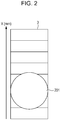
- the photoelectric sensor when light is emitted from the light-emitting device 2 to a detection area and the light is reflected by a detection object present in the detection area, the light is received by the multi-segment photodiode 3 (on a light-receiving spot 201) as illustrated in Fig. 2 , for example.
- the current divider circuits 4 are respectively connected to the photodiodes PD that constitute the multi-segment photodiode 3.
- the current that flows through the corresponding photodiode PD can be divided into the first current to be diverted into the IV amplifier 6 and the second current to be diverted into the IV amplifier 7.
- the first currents divided by the respective current divider circuits 4 are added together and the sum of the first currents is converted into a voltage by the IV amplifier 6, and the second currents divided by the respective current divider circuits 4 are added together and the sum of the second currents is converted into a voltage by the IV amplifier 7. Thereafter, the voltage difference between the voltages is detected by the arithmetic circuit 8.
- the position of the light-receiving spot 201 on the multi-segment photodiode 3 changes in accordance with the distance to the detection object. Therefore, with the above-described voltage difference, it is possible to detect a detection object on the basis of the distance instead of the amount of light.
- FIG. 3A and 3B A relationship between the output v1 (represented by a solid line) of the IV amplifier 6 and the output v2 (represented by a dashed line) of the IV amplifier 7 when the position of the light-receiving spot 201 on the multi-segment photodiode 3 moves in the x direction illustrated in Fig. 2 is illustrated in Figs. 3A and 3B .
- the control voltage Vcnt is set to 1.7 V in Fig. 3A
- the control voltage Vcnt is set to 1.8 V in Fig. 3B .
- Vcnt 1.8 V
- the photodiodes PD have a length of 0.3 mm, it is possible to detect the difference in a case where the position of the light-receiving spot 201 changes and is positioned at the distance of 1.35 mm from the distance of 1.2 mm. That is, by using the current divider circuits 4, the set interval for the detection range can be set to a range smaller than the length of the photodiodes PD, and the resolution can be increased accordingly.
- Fig. 4 illustrates an example configuration of the current division control circuit 12 that serves eight current divider circuits 4.
- the current division control circuit 12 includes a plurality of reference voltage generation resistors R1 (R1_1 to R1_9), a plurality of reference voltage output lines l1 (l1_1 to l1_8), a control voltage generation circuit 121, a switch group 122 constituted by a plurality of switches sw1 (sw1_0 to sw1_9), a plurality of resistors R2 (R2_1 to R2_9), and two resistors R3 (R3_1 and R3_2), as illustrated in Fig. 4 .
- the reference voltage generation resistors R1 are connected in series between two voltages (VH and VL). With the plurality of reference voltage generation resistors R1, voltage division on the basis of the two voltages is performed. In a case k current divider circuits 4 are provided, k + 1 reference voltage generation resistors R1 are provided. The reference voltage generation resistors R1 that are used have the same resistance.
- VH and VL are set to values appropriate to the circuit operation. That is, the values of VH and VL are set so as to match a voltage range for normal operations upon input to and output from the current divider circuits 4 and the IV amplifies 6 and 7.
- a circuit (transistor) not illustrated is connected through which a bias current for ensuring a response speed flows.
- the current divider circuits 4 may be in the saturation region and may fail to operate normally.
- the input voltage range of the IV amplifiers 6 and 7 has an upper limit, and it is not possible to set the input voltage to a very high value. Therefore, the reference voltages Vref and the control voltage Vcnt need to be determined by taking into consideration the above-described conditions, and the values of VH and VL are also determined by taking into consideration the conditions.
- the reference voltage output lines l1 are used to output voltages divided by the reference voltage generation resistors R1 as reference voltages.
- one end of each of the reference voltage output lines l1 is connected between corresponding ones of the reference voltage generation resistors R1, and the other end thereof is connected to the base terminal of the transistor Tr1 of a corresponding one of the current divider circuits 4.
- the control voltage generation circuit 121 has the function of the reference voltage generation resistors R1 and a function of generating the control voltage that falls between the connected voltages.
- An example configuration of the control voltage generation circuit 121 is described below.
- the switch group 122 is used to replace one of the reference voltage generation resistors R1 with the control voltage generation circuit 121 in accordance with control signals (cntl0 to cntl9) from the control logic circuit 13.
- the resistors R2 are respectively connected in parallel to the reference voltage generation resistors R1. Note that the resistors R2 that are used have the same resistance, which is equal to about one-tenth of the resistance of the reference voltage generation resistors R1.
- the resistors R3 are respectively connected in series to the reference voltage generation resistors R1 that are positioned at the respective ends.
- the control voltage generation circuit 121 includes a pair of connection lines l2 (l2_1 and l2_2), a plurality of control voltage generation resistors R4 (R4_1 to R4_n), a switch group 1211 constituted by a plurality of switches sw2 (sw2_1 to sw2_n), and a control voltage output line 13.
- connection lines l2 When one of the reference voltage generation resistors R1 is replaced with the control voltage generation circuit 121 in accordance with an operation of the switch group 122, one end of one of the connection lines l2 is connected to one of the reference voltage generation resistors R1 adjacent to the replaced reference voltage generation resistor R1, and one end of the other connection line l2 is connected to the other reference voltage generation resistor R1 adjacent to the replaced reference voltage generation resistor R1.
- the control voltage generation resistors R4 are connected in series between the connection lines 12. With the plurality of control voltage generation resistors R4, the voltage between the connection lines l2 is divided. Note that the sum of the resistances of the control voltage generation resistors R4 is made equal to the resistance of the reference voltage generation resistors R1. By using the control voltage generation resistors R4, the adjustment step for the control voltage is made smaller.
- the switch group 1211 is used to select one of the voltages divided by the control voltage generation resistors R4 as the control voltage in accordance with a control signal (cntl_b) from the control logic circuit 13.
- the control voltage output line l3 is used to output the control voltage selected by the switch group 1211 to the base terminal of the transistor Tr2 of each of the current divider circuits 4.
- One end of the control voltage output line l3 is connected to the output end of each of the switches sw1 that constitute the switch group 1211, and the other end thereof is connected to the base terminal of the transistor Tr2 of each of the current divider circuits 4.
- the control logic circuit 13 outputs the control signals cntl0 to cntl9 for the switch group 122 and outputs the control signal cntl_b for the switch group 1211.
- the control signals cntl1 to cntl8 are assumed to be signals having two bits or more because there are three states which the switches sw1_1 to sw1_8 may enter, and the control signals cntl0 and cntl9 are assumed to be signals having one bit or more because there are two states which the switches sw1_0 to sw1_9 may enter.
- the reference voltage generation resistor R1_6 is disconnected and the control voltage generation circuit 121 is connected instead in accordance with operations of the switches sw1_5 and sw1_6, for example, as illustrated in Fig. 5 .
- the control voltage generation circuit 121 is connected instead of the reference voltage generation resistor R1_6 in series between the other reference voltage generation resistors R1.
- a voltage between Vref5 and Vref6 can be selected as the control voltage.
- a voltage Vref9 that is higher than the reference voltages Vref1 to Vref8 respectively used by the current divider circuits 4 and a voltage Vref0 that is lower than the reference voltages Vref1 to Vref8 are set, and the control voltage generation circuit 121 can select the control voltage from within a range between the voltage Vref0 and the voltage Vref9. Accordingly, it is possible to maximize the range within which the set distance can be set.
- the current division control circuit 12 is provided that sequentially sets the reference voltage for each current divider circuit 4 along one of the arrangement directions of the photodiodes PD so that the reference voltage for the current divider circuit 4 is equal to or larger than the voltage value of the reference voltage set for the current divider circuit 4 in the preceding stage, and that sets one common control voltage for all of the current divider circuits 4, the common control voltage falling within a range that includes all of the reference voltages. Therefore, the reference voltages and the control voltage can be digitally adjusted, and it is possible to set the current division ratios of the current divider circuits 4 more efficiently with higher accuracy in the photoelectric sensor including the current divider circuits 4 compared to the related-art configuration.
- the resistance of the reference voltage generation resistors R1 needs to be set to a sufficiently large value relative to the on-resistance of the switches sw1 that constitute the switch group 122.
- the resistors R2 are respectively connected in parallel to the reference voltage generation resistors R1 in the embodiments of the present invention. Accordingly, even if the resistance of the reference voltage generation resistors R1 is increased, the impedances of the reference voltages can be decreased, and the impact on the base currents flowing through the connected current divider circuits 4 can be reduced.
- data based on which output is turned on is determined while data input to the control logic circuit 13 is scanned by using an external microcomputer or the like (tuning), the determined data is input as set data for the control logic circuit 13, and the control logic circuit 13 uses the input data to thereby adjust the reference voltages and the control voltage based on which the current division ratios of the current divider circuits 4 are determined.
- automatic setting auto-tuning
- setting accuracy can be increased, and reproducibility can be ensured accordingly.
- Each of the current divider circuits 4 operates in accordance with the difference between the base voltages of the two transistors Tr1 and Tr2, which constitute a differential pair. Accordingly, by setting the control voltage and the reference voltages on the basis of the same set of voltages so as to fall between the voltages, the circuit can be less affected by fluctuations or the like in the voltages.
- the current divider circuits 4 each have a property such that, if the difference between the base voltages of the transistors Tr1 and Tr2 exceeds 0.2 V, most of the current from the photodiode PD flows through the transistor having a higher base voltage. Therefore, the set interval between the reference voltages may be set to a value between 0.05 V and 0.2 V, for example.
- FIG. 6 In a second embodiment, another example configuration of the current division control circuit 12 is described with reference to Fig. 6 .
- Fig. 6 In the example illustrated in Fig. 6 , an example configuration of the current division control circuit 12 that serves eight current divider circuits 4 is illustrated.
- the current division control circuit 12 in the second embodiment includes a plurality of reference voltage generation resistors R5 (R5_1 to R5_4), the control voltage generation circuit 121, a switch switching circuit 123, the plurality of reference voltage output lines l1 (l1_1 to l1_8), a plurality of resistors R6 (R6_1 to R6_5), and two resistors R7 (R7_1 and R7_2), as illustrated in Fig. 6 .
- the reference voltage generation resistors R5 are connected in series between the two voltages (VH and VL).
- the number of the reference voltage generation resistors R5 that are provided is smaller than the number of the current divider circuits 4. Note that the reference voltage generation resistors R5 that are used have the same resistance.
- the control voltage generation circuit 121 is connected in series to or between the reference voltage generation resistors R5 and has the function of the reference voltage generation resistors R5 and the function of generating the control voltage that falls between the connected voltages.
- the control voltage generation circuit 121 may be connected to any position between the above-described two voltages. With the plurality of reference voltage generation resistors R5 and the control voltage generation circuit 121, voltage division on the basis of the two voltages is performed. Note that the configuration of the control voltage generation circuit 121 is similar to the configuration illustrated in Fig. 4 , and description thereof is omitted.
- the switch switching circuit 123 distributes the voltages divided by the reference voltage generation resistors R5 and the control voltage generation circuit 121 as the reference voltages for the respective current divider circuits 4 in accordance with a control signal (cntl) from the control logic circuit 13.
- the reference voltage output lines l1 are used to output the reference voltages distributed by the switch switching circuit 123 to the current divider circuits 4 respectively.
- One end of each of the reference voltage output lines l1 is connected to a corresponding one of the output ends of the switch switching circuit 123, and the other end thereof is connected to the base terminal of the transistor Tr1 of a corresponding one of the current divider circuits 4.
- resistors R6 is connected in parallel to the control voltage generation circuit 121 and the other resistors R6 are respectively connected in parallel to the reference voltage generation resistors R5. Note that the resistors R6 that are used have the same resistance, which is equal to about one-tenth of the resistance of the reference voltage generation resistors R5.
- the resistors R7 are respectively connected in series to the reference voltage generation resistors R5 that are positioned at the respective ends (or one of the resistors R7 is connected in series to the control voltage generation circuit 121 if the control voltage generation circuit 121 is positioned at one of the ends).
- the control logic circuit 13 outputs the control signal cntl for the switch switching circuit 123 and the control signal cntl_b for the switch group 1211.
- the current divider circuits 4 each have a property such that, if the difference between the base voltages of the transistors Tr1 and Tr2 reaches or exceeds 0.2 V, most of the current from the photodiode PD flows through one of the transistors. Therefore, in a case where the current divider circuit 4 having the base voltage difference of 0.2 V and the current divider circuit 4 having the base voltage difference of 0.3 V are present, even if the reverence voltages are changed so that both the base voltage differences are equal to 0.2 V, the error in the result of current division is at a level that requires no attention. Therefore, the reference voltages that are apart from the control voltage by 0.2 V or more can be set to the same value.
- the control voltage is a voltage between Vref4 and Vref5. Therefore, as illustrated in Fig. 7A , in the current divider circuits 4 to which the reference voltages Vref8 and Vref1 are applied respectively, even if the reference voltage Vref8 is changed to Vref7 and the reference voltage Vref1 is changed to Vref2, the values of the divided currents consequently remain substantially unchanged.
- the embodiments of the present invention are not limited to the case. Even if the resistances of the reference voltage generation resistors R5 are not equal to one another and the resistances of the resistors R6 are not equal to one another, the current division operation is performed. However, the result obtained in this case is different from the case where the resistances are made equal to one another.
- the configuration is employed in which some of the reference voltages for the current divider circuits 4 are set to the same value by taking advantage of the property of the current divider circuits 4. Therefore, the effect attained by the first embodiment is also attained, and the circuit scale can be reduced. Further, the voltages used to generate the reference voltages and the control voltage can be decreased.
- control voltage generation circuit 121 In a third embodiment, another example configuration of the control voltage generation circuit 121 is described with reference to Fig. 8 .
- the control voltage generation circuit 121 in the third embodiment includes the pair of connection lines l2 (l2_1 and l2_2), a plurality of first control voltage generation resistors R8 (R8_1 to R8_8), a voltage divider circuit 1212, and a switch group 1213 constituted by a plurality of switches sw3 (sw3_0 to sw3_9), as illustrated in Fig. 8 .
- a case where the control voltage generation circuit 121 is applied to the current division control circuit 12 according to the first embodiment is described below.
- connection lines l2 When one of the reference voltage generation resistors R1 is replaced with the control voltage generation circuit 121 in accordance with an operation of the switch group 122, one end of one of the connection lines l2 is connected to one of the reference voltage generation resistors R1 adjacent to the replaced reference voltage generation resistor R1, and one end of the other connection line l2 is connected to the other reference voltage generation resistor R1 adjacent to the replaced reference voltage generation resistor R1.
- the first control voltage generation resistors R8 are connected in series between the connection lines 12. With the plurality of first control voltage generation resistors R8, the voltage between the connection lines l2 is divided. Note that the sum of the resistances of the first control voltage generation resistors R8 is made equal to the resistance of the reference voltage generation resistors R1. By using the first control voltage generation resistors R8, the adjustment step for the control voltage can be made smaller.
- the voltage divider circuit 1212 has the function of the first control voltage generation resistors R8 and the function of generating the control voltage that falls between the connected voltages.
- An example configuration of the voltage divider circuit 1212 is described below.
- the switch group 1213 is used to replace one of the first control voltage generation resistors R8 with the voltage divider circuit 1212 in accordance with control signals (cntl10 to cntl18) from the control logic circuit 13.
- the voltage divider circuit 1212 includes a pair of connection lines l4 (l4_1 and l4_2), a plurality of second control voltage generation resistors R9 (R9_1 to R9_n), a switch group 12121 constituted by a plurality of switches sw4 (sw4_1 to sw4_n), and the control voltage output line 13.
- connection lines l4 When one of the first control voltage generation resistors R8 is replaced with the voltage divider circuit 1212 in accordance with an operation of the switch group 1213, one end of one of the connection lines l4 is connected to one of the first control voltage generation resistors R8 adjacent to the replaced first control voltage generation resistor R8, and one end of the other connection line l4 is connected to the other first control voltage generation resistor R8 adjacent to the replaced first control voltage generation resistor R8.
- the second control voltage generation resistors R9 are connected in series between the connection lines l4. With the plurality of second control voltage generation resistors R9, the voltage between the connection lines l4 is divided. Note that the sum of the resistances of the second control voltage generation resistors R9 is made equal to the resistance of the first control voltage generation resistors R8. By using the second control voltage generation resistors R9, the adjustment step for the control voltage can be further made smaller.
- the switch group 12121 is used to select one of the voltages divided by the second control voltage generation resistors R9 as the control voltage in accordance with the control signal (cntl_b) from the control logic circuit 13.
- the control voltage output line l3 is used to output the control voltage selected by the switch group 12121 to the base terminal of the transistor Tr2 of each of the current divider circuits 4.
- One end of the control voltage output line l3 is connected to the output end of each of the switches sw4 that constitute the switch group 12121, and the other end thereof is connected to the base terminal of the transistor Tr2 of each of the current divider circuits 4.
- the control logic circuit 13 outputs the control signals cntl0 to cntl9 for the switch group 122 and outputs the control signals cntl1 0 to cntl18 and cntl_b for the switch groups 1213 and 12121.
- the voltage is divided by the resistors R4 connected in series between the connection lines l2.
- the resistors R4 In order to provide 64-step switching, for example, 63 resistors R4 and 64 switches sw2 are necessary.
- the voltage is divided in two stages. Accordingly, in a circuit capable of providing the same 64-step switching, the number of the resistors R8 and R9 can be decreased to 16, and the number of the switches sw3 and sw4 can be decreased to 40.
- switches sw3_1 to sw3_7 are four-pole switches, and therefore, each of the switches sw3_1 to sw3_7 is counted as four switches. Each of the switches sw3_0 and sw3_9 is counted as two switches.
- control voltage generation circuit 121 is provided so as to divide the voltage in two stages. Therefore, a higher resolution can be provided to the control voltage, and the circuit scale can be reduced compared to the first embodiment.
- control voltage generation circuit 121 according to the third embodiment illustrated in Fig. 8 is applied to the current division control circuit 12 according to the first embodiment
- control voltage generation circuit 121 according to the third embodiment may be applied to the current division control circuit 12 according to the second embodiment, and a similar effect can also be attained in this case.
- the current division control circuit 12 generates the control voltage and the reference voltages in accordance with the voltage division using the resistors. Therefore, in a case where a large current flows into the current divider circuit 4, the base currents flow through the transistors Tr1 and Tr2 of the current divider circuit 4, and the error may become large. In a fourth embodiment, a configuration for correcting such a situation is described.
- Fig. 9 is a diagram illustrating an example configuration of the current division control circuit 12 according to the fourth embodiment of the present invention.
- the current division control circuit 12 according to the fourth embodiment illustrated in Fig. 9 is configured on the basis of the current division control circuit 12 according to the second embodiment illustrated in Fig. 6 and further includes buffer circuits 124 and 125.
- the components other than the buffer circuits 124 and 125 are similarly configured. Therefore, the components are similarly assigned the reference numerals, and description thereof is omitted.
- the buffer circuit 124 is provided to output the reference voltages.
- the buffer circuit 124 includes a plurality of current sources Is1 (ls1_1 to Is1_8) and a plurality of transistors Tr3 (Tr3_1 to Tr3_8), as illustrated in Fig. 9 .
- the current sources Is1 each supply a constant current.
- Each of the transistors Tr3 has a base terminal that is connected to a corresponding one of the reference voltage output lines l1, an emitter terminal that is connected to a corresponding one of the current sources Is1, and a collector terminal to which a supply voltage Vcc is applied.
- the buffer circuit 125 is provided to output the control voltage.
- the buffer circuit 125 includes a current source Is2 and a transistor Tr4, as illustrated in Fig. 9 .
- the current source Is2 supplies a constant current.
- the transistor Tr4 has a base terminal that is connected to the output end of each of the switches sw1 that constitute the switch group 1211, an emitter terminal that is connected to the current source Is2, and a collector terminal to which the supply voltage Vcc is applied.
- the buffer circuits 124 and 125 are respectively provided to output the reference voltages and to output the control voltage. As a result, even in the case where a large current flows into the current divider circuit 4, the error can be reduced.
- the buffer circuits 124 and 125 may be applied to the current division control circuit 12 according to the first embodiment, and a similar effect can also be attained in this case.
- the photoelectric sensor is not limited to a BGS-type photoelectric sensor.
- the embodiments of the present invention are also applicable to foreground suppression (FGS)-type photoelectric sensors that detect a detection object present at a distance more than a set distance.
- FGS foreground suppression
Landscapes
- Physics & Mathematics (AREA)
- Engineering & Computer Science (AREA)
- Electromagnetism (AREA)
- General Physics & Mathematics (AREA)
- Radar, Positioning & Navigation (AREA)
- Remote Sensing (AREA)
- Computer Networks & Wireless Communication (AREA)
- Automation & Control Theory (AREA)
- Life Sciences & Earth Sciences (AREA)
- General Life Sciences & Earth Sciences (AREA)
- Geophysics (AREA)
- Measurement Of Optical Distance (AREA)
- Electronic Switches (AREA)
- Analogue/Digital Conversion (AREA)
Claims (7)
- Fotoelektrischer Sensor mit einem Nachweisbereich für ein Nachweisobjekt, eingestellt durch die Verwendung einer eingestellten Distanz, wobei der fotoelektrische Sensor Folgendes umfasst:eine Mehrsegment-Photodiode (3), in der eine Vielzahl von Photodioden ein einer Anordnungsrichtung angeordnet ist,eine Vielzahl von Stromteilerkreisen (4), die jeweils mit der Vielzahl von Photodioden verbunden sind und jeweils ein Stromteilungsverhältnis aufweisen, das in Übereinstimmung mit einer Differenz zwischen einer Referenzspannung und einer Steuerspannung eingestellt ist; undeine Stromteilungs-Steuereinheit (12), die ausgelegt ist, um die Referenzspannung für jeden Stromteilerkreis (4) aus der Vielzahl von Stromteilerkreisen (4) entlang der Anordnungsrichtung der Photodioden sequentiell einzustellen, so dass die Referenzspannung für den Stromteilerkreis (4) gleich wie oder größer als ein Spannungswert der Referenzspannung ist, der für einen Stromteilerkreis (4) in einer unmittelbar vorhergehenden Position in der Anordnungsrichtung aus der Vielzahl von Stromteilerkreisen (4) eingestellt ist, und um die Steuerspannung, wobei es sich um eine gemeinsame Steuerspannung handelt, für alle der Vielzahl von Stromteilerkreisen (4) einzustellen, wobei die gemeinsame Steuerspannung in einen Bereich fällt, der alle der Referenzspannungen einschließt, dadurch gekennzeichnet, dassder Stromteilungs-Steuerkreis (12) Folgendes einschließt:eine Vielzahl von Referenzspannungs-Generationswiderständen, die zwischen zwei Spannungen in Reihe verbunden sind,eine Vielzahl von Referenzspannungs-Ausgabeleitungen, die verwendet werden, um Spannungen, geteilt durch die Referenzspannungs-Generationswiderstände, als die Referenzspannungen auszugeben,ein Steuerspannungs-Generationskreis (121), der mit den Referenzspannungs-Generationswiderständen verbunden und ausgelegt ist, um die Steuerspannung zu generieren, die zwischen verbundene Spannungen fällt, undeine Schaltgruppe, die verwendet wird, um einen der Referenzspannungs-Generationswiderstände zu teilen und den Steuerspannungs-Generationskreis (121) stattdessen zu verbinden.
- Photoelektrischer Sensor nach Anspruch 1, wobei
der Stromteilungs-Steuerkreis (12) weiter einschließt:
eine Vielzahl von Widerständen, die jeweils mit den Referenzspannungs-Generationswiderständen parallel verbunden sind. - Fotoelektrischer Sensor mit einem Nachweisbereich für ein Nachweisobjekt, eingestellt durch die Verwendung einer eingestellten Distanz, wobei der fotoelektrische Sensor Folgendes umfasst:eine Mehrsegment-Photodiode (3), in der eine Vielzahl von Photodioden ein einer Anordnungsrichtung angeordnet ist,eine Vielzahl von Stromteilerkreisen (4), die jeweils mit der Vielzahl von Photodioden verbunden sind und jeweils ein Stromteilungsverhältnis aufweisen, das in Übereinstimmung mit einer Differenz zwischen einer Referenzspannung und einer Steuerspannung eingestellt ist; undeinen Stromteilungs-Steuerkreis (12), die ausgelegt ist, um die Referenzspannung für jeden Stromteilerkreis (4) aus der Vielzahl von Stromteilerkreisen (4) entlang der Anordnungsrichtung der Photodioden einzustellen, so dass die Referenzspannung für den Stromteilerkreis (4) gleich oder größer als ein Spannungswert der Referenzspannung ist, die für einen Stromteilerkreis (4) in einer unmittelbar vorausgehenden Position in der Anordnungsrichtung aus der Vielzahl von Stromteilerkreisen (4) eingestellt ist, und um die Steuerspannung, wobei es sich um eine gemeinsame Steuerspannung handelt, für alle der Vielzahl von Stromteilerkreisen (4) einzustellen, wobei die gemeinsame Steuerspannung in einen Bereich fällt, der alle der Referenzspannungen einschließt, dadurch gekennzeichnet, dassder Stromteilungs-Steuerkreis (12) Folgendes einschließt:eine Vielzahl von Referenzspannungs-Generationswiderständen, die zwischen zwei Spannungen in Reihe verbunden sind,ein Steuerspannungs-Generationskreis (121), der an oder zwischen den Referenzspannungs-Generatonswiderständen verbunden und ausgelegt ist, um die Steuerspannung zu generieren, die zwischen verbundene Spannungen fällt, undeinen Schalter-Schaltkreis, der Spannungen, geteilt durch die Referenzspannungs-Generationswiderstände und den Steuerspannungs-Generationskreis (121), als die Referenzspannungen für die entsprechenden Stromteilerkreise (4) verteilt.
- Photoelektrischer Sensor nach Anspruch 3, wobei
der Stromteilungs-Steuerkreis (12) weiter einschließt:
eine Vielzahl von Widerständen, wobei einer der Widerstände an den Steuerspannungs-Genarationskreis (121) parallel verbunden ist, wobei Widerstände aus den Widerständen außer dem einen der Widerstände jeweils an die Referenzspanungs-Generationswiderstände parallel verbunden sind. - Photoelektrischer Sensor nach einem der Ansprüche 1 bis 4, wobei
der Steuerspannungs-Generationskreis (121), Folgendes einschließt:eine Vielzahl von Referenzspannungs-Generationswiderständen, die zwischen die verbundenen Spannungen in Reihe verbunden sind, undeine Schaltgruppe, die verwendet wird, um eine der Spannungen, geteilt durch die Steuerspannungs-Generationswiderstände, als die Steuerspannung auszuwählen. - Photoelektrischer Sensor nach einem der Ansprüche 1 bis 4, wobei der Steuerspannungs-Generationskreis (121) Folgendes einschließt:eine Vielzahl von ersten Steuerspannungs-Generationswiderständen, die zwischen den verbundenen Spannungen in Reihe verbunden sind,einen Spannungsteilerkreis (1212), der eine Funktion des Generierens der Steuerspannung aufweist, die zwischen verbundene zweite Spannungen fällt, undeine Schaltgruppe, die verwendet wird, um einen der ersten Steuerspannungs-Generationswiderstände durch den Spannungsteilerkreis (1212) zu ersetzen, wobeider Spannungsteilerkreis (1212) Folgendes umfasst:eine Vielzahl von zweiten Steuerspannungs-Generationswiderständen, die zwischen den verbundenen zweiten Spannungen in Reihe verbunden sind, undeine Schaltgruppe, die verwendet wird, um eine der Spannungen, geteilt durch die zweiten Steuerspannungs-Generationswiderstände. als die Steuerspannung auszuwählen.
- Photoelektrischer Sensor nach einem der Ansprüche 1 bis 6, wobei der Stromteilungs-Steuerkreis(12) Folgendes einschließt:einen Pufferkreis, der bereitgestellt ist, um die Referenzspannungen auszugeben, undeinen Pufferkreis, der bereitgestellt ist, um die Steuerspannung auszugeben.
Applications Claiming Priority (1)
| Application Number | Priority Date | Filing Date | Title |
|---|---|---|---|
| JP2015139601A JP6501659B2 (ja) | 2015-07-13 | 2015-07-13 | 光電センサ |
Publications (2)
| Publication Number | Publication Date |
|---|---|
| EP3118652A1 EP3118652A1 (de) | 2017-01-18 |
| EP3118652B1 true EP3118652B1 (de) | 2020-05-27 |
Family
ID=56360210
Family Applications (1)
| Application Number | Title | Priority Date | Filing Date |
|---|---|---|---|
| EP16177564.8A Active EP3118652B1 (de) | 2015-07-13 | 2016-07-01 | Fotoelektrischer sensor |
Country Status (4)
| Country | Link |
|---|---|
| US (1) | US9905595B2 (de) |
| EP (1) | EP3118652B1 (de) |
| JP (1) | JP6501659B2 (de) |
| CN (1) | CN106353835B (de) |
Families Citing this family (3)
| Publication number | Priority date | Publication date | Assignee | Title |
|---|---|---|---|---|
| US12393217B2 (en) * | 2018-11-09 | 2025-08-19 | Ian R. Vinci | Load current simulator |
| CN114337675A (zh) * | 2022-03-14 | 2022-04-12 | 四川奥库科技有限公司 | 三段电阻型数模转换器电路 |
| US12442841B2 (en) * | 2022-06-30 | 2025-10-14 | Avago Technologies International Sales Pte. Limited | Current sensing circuit with integrated resistor and dual sense amplifiers |
Family Cites Families (14)
| Publication number | Priority date | Publication date | Assignee | Title |
|---|---|---|---|---|
| GB2211047B (en) * | 1987-10-12 | 1992-08-12 | Fuji Photo Film Co Ltd | Distance measuring device |
| JPH0247909A (ja) * | 1988-08-08 | 1990-02-16 | Nec Corp | 基準電圧の発生回路 |
| JPH05175849A (ja) * | 1991-06-18 | 1993-07-13 | Fujitsu Ltd | Daコンバータ |
| JP2933804B2 (ja) * | 1993-08-03 | 1999-08-16 | 株式会社山武 | 光電スイッチ |
| JP3215232B2 (ja) * | 1993-08-03 | 2001-10-02 | 株式会社山武 | 光電式距離センサ |
| US6407817B1 (en) * | 1993-12-20 | 2002-06-18 | Minolta Co., Ltd. | Measuring system with improved method of reading image data of an object |
| JPH07336226A (ja) * | 1994-06-03 | 1995-12-22 | Hitachi Ltd | 分圧回路、及びa/d変換器、並びに半導体集積回路 |
| JP4011686B2 (ja) * | 1997-09-30 | 2007-11-21 | セイコープレシジョン株式会社 | カメラ用測距装置 |
| US5969338A (en) * | 1998-03-18 | 1999-10-19 | Sanyo Electric Co., Ltd. | Light-received position detecting circuit and distance detecting apparatus using the same |
| JP3281621B2 (ja) * | 1999-12-21 | 2002-05-13 | 松下電器産業株式会社 | 高精度da変換回路 |
| US6414616B1 (en) * | 2000-06-22 | 2002-07-02 | Analog Devices, Inc. | Architecture for voltage scaling DAC |
| JP3999045B2 (ja) * | 2002-05-24 | 2007-10-31 | 日本信号株式会社 | 物体検出装置 |
| JP4569647B2 (ja) * | 2008-03-18 | 2010-10-27 | ソニー株式会社 | Ad変換装置、ad変換方法、固体撮像素子、およびカメラシステム |
| JP6196794B2 (ja) * | 2013-03-29 | 2017-09-13 | ローム株式会社 | D/aコンバータ |
-
2015
- 2015-07-13 JP JP2015139601A patent/JP6501659B2/ja active Active
-
2016
- 2016-07-01 EP EP16177564.8A patent/EP3118652B1/de active Active
- 2016-07-12 US US15/208,279 patent/US9905595B2/en active Active
- 2016-07-13 CN CN201610550727.6A patent/CN106353835B/zh active Active
Non-Patent Citations (1)
| Title |
|---|
| None * |
Also Published As
| Publication number | Publication date |
|---|---|
| CN106353835A (zh) | 2017-01-25 |
| JP6501659B2 (ja) | 2019-04-17 |
| US20170018586A1 (en) | 2017-01-19 |
| US9905595B2 (en) | 2018-02-27 |
| CN106353835B (zh) | 2018-09-25 |
| JP2017022594A (ja) | 2017-01-26 |
| EP3118652A1 (de) | 2017-01-18 |
Similar Documents
| Publication | Publication Date | Title |
|---|---|---|
| KR20160112415A (ko) | 전류 추가 기능을 가지는 비교 장치 및 그를 이용한 아날로그-디지털 변환 시스템 | |
| JP2022101408A (ja) | 固体撮像装置、ad変換回路および電流補償回路 | |
| EP3118652A1 (de) | Fotoelektrischer sensor | |
| US11968465B2 (en) | Solid-state image sensing device including a column-parallel A/D converting circuit | |
| US6831580B2 (en) | Digital-to-analog converter with linear amplification rate | |
| US5498993A (en) | Pulse light-receiving circuit with means to minimize power source noise | |
| US9584110B2 (en) | Reference voltage generator having noise cancelling function and CMOS image sensor using the same | |
| JP7787653B2 (ja) | イメージセンサ及びアナログ-デジタル変換器 | |
| JPH0953984A (ja) | 輝度検出回路 | |
| US6417503B1 (en) | Optical sensor circuit with output changing means | |
| US20080054169A1 (en) | Optical encoder | |
| JP4002581B2 (ja) | 光電式エンコーダおよび電子機器 | |
| US6711352B2 (en) | Range finder of light amount detection type with multi zone resolution | |
| EP1511197A2 (de) | Photoelektrischer Strom und Spannungsumwandlerschaltung | |
| US6956195B2 (en) | Photoelectric current and voltage converting circuit | |
| US7247834B2 (en) | Photoelectric sensor for detecting presence/absence of object | |
| JP2004260230A (ja) | 光電流・電圧変換回路 | |
| JP2010183345A (ja) | トランスインピーダンス増幅器及びアナログ/デジタル変換回路 | |
| JPH1146011A (ja) | 受光位置検出回路 | |
| JP4221716B2 (ja) | 光論理素子 | |
| JP2020148551A (ja) | 光検出装置および光学エンコーダ装置 | |
| JP2017022595A (ja) | 光電センサ | |
| JP3117232B2 (ja) | 測距装置 | |
| KR102853721B1 (ko) | 아날로그-디지털 변환 회로 및 이미지 센서 | |
| JP2009200667A (ja) | 信号増幅回路 |
Legal Events
| Date | Code | Title | Description |
|---|---|---|---|
| PUAI | Public reference made under article 153(3) epc to a published international application that has entered the european phase |
Free format text: ORIGINAL CODE: 0009012 |
|
| STAA | Information on the status of an ep patent application or granted ep patent |
Free format text: STATUS: THE APPLICATION HAS BEEN PUBLISHED |
|
| AK | Designated contracting states |
Kind code of ref document: A1 Designated state(s): AL AT BE BG CH CY CZ DE DK EE ES FI FR GB GR HR HU IE IS IT LI LT LU LV MC MK MT NL NO PL PT RO RS SE SI SK SM TR |
|
| AX | Request for extension of the european patent |
Extension state: BA ME |
|
| STAA | Information on the status of an ep patent application or granted ep patent |
Free format text: STATUS: REQUEST FOR EXAMINATION WAS MADE |
|
| 17P | Request for examination filed |
Effective date: 20170407 |
|
| RBV | Designated contracting states (corrected) |
Designated state(s): AL AT BE BG CH CY CZ DE DK EE ES FI FR GB GR HR HU IE IS IT LI LT LU LV MC MK MT NL NO PL PT RO RS SE SI SK SM TR |
|
| GRAP | Despatch of communication of intention to grant a patent |
Free format text: ORIGINAL CODE: EPIDOSNIGR1 |
|
| STAA | Information on the status of an ep patent application or granted ep patent |
Free format text: STATUS: GRANT OF PATENT IS INTENDED |
|
| INTG | Intention to grant announced |
Effective date: 20200109 |
|
| GRAS | Grant fee paid |
Free format text: ORIGINAL CODE: EPIDOSNIGR3 |
|
| GRAA | (expected) grant |
Free format text: ORIGINAL CODE: 0009210 |
|
| STAA | Information on the status of an ep patent application or granted ep patent |
Free format text: STATUS: THE PATENT HAS BEEN GRANTED |
|
| AK | Designated contracting states |
Kind code of ref document: B1 Designated state(s): AL AT BE BG CH CY CZ DE DK EE ES FI FR GB GR HR HU IE IS IT LI LT LU LV MC MK MT NL NO PL PT RO RS SE SI SK SM TR |
|
| REG | Reference to a national code |
Ref country code: GB Ref legal event code: FG4D |
|
| REG | Reference to a national code |
Ref country code: CH Ref legal event code: EP |
|
| REG | Reference to a national code |
Ref country code: AT Ref legal event code: REF Ref document number: 1275105 Country of ref document: AT Kind code of ref document: T Effective date: 20200615 |
|
| REG | Reference to a national code |
Ref country code: DE Ref legal event code: R096 Ref document number: 602016036923 Country of ref document: DE |
|
| REG | Reference to a national code |
Ref country code: LT Ref legal event code: MG4D |
|
| PG25 | Lapsed in a contracting state [announced via postgrant information from national office to epo] |
Ref country code: FI Free format text: LAPSE BECAUSE OF FAILURE TO SUBMIT A TRANSLATION OF THE DESCRIPTION OR TO PAY THE FEE WITHIN THE PRESCRIBED TIME-LIMIT Effective date: 20200527 Ref country code: LT Free format text: LAPSE BECAUSE OF FAILURE TO SUBMIT A TRANSLATION OF THE DESCRIPTION OR TO PAY THE FEE WITHIN THE PRESCRIBED TIME-LIMIT Effective date: 20200527 Ref country code: PT Free format text: LAPSE BECAUSE OF FAILURE TO SUBMIT A TRANSLATION OF THE DESCRIPTION OR TO PAY THE FEE WITHIN THE PRESCRIBED TIME-LIMIT Effective date: 20200928 Ref country code: SE Free format text: LAPSE BECAUSE OF FAILURE TO SUBMIT A TRANSLATION OF THE DESCRIPTION OR TO PAY THE FEE WITHIN THE PRESCRIBED TIME-LIMIT Effective date: 20200527 Ref country code: IS Free format text: LAPSE BECAUSE OF FAILURE TO SUBMIT A TRANSLATION OF THE DESCRIPTION OR TO PAY THE FEE WITHIN THE PRESCRIBED TIME-LIMIT Effective date: 20200927 Ref country code: NO Free format text: LAPSE BECAUSE OF FAILURE TO SUBMIT A TRANSLATION OF THE DESCRIPTION OR TO PAY THE FEE WITHIN THE PRESCRIBED TIME-LIMIT Effective date: 20200827 Ref country code: GR Free format text: LAPSE BECAUSE OF FAILURE TO SUBMIT A TRANSLATION OF THE DESCRIPTION OR TO PAY THE FEE WITHIN THE PRESCRIBED TIME-LIMIT Effective date: 20200828 |
|
| REG | Reference to a national code |
Ref country code: NL Ref legal event code: MP Effective date: 20200527 |
|
| PG25 | Lapsed in a contracting state [announced via postgrant information from national office to epo] |
Ref country code: HR Free format text: LAPSE BECAUSE OF FAILURE TO SUBMIT A TRANSLATION OF THE DESCRIPTION OR TO PAY THE FEE WITHIN THE PRESCRIBED TIME-LIMIT Effective date: 20200527 Ref country code: RS Free format text: LAPSE BECAUSE OF FAILURE TO SUBMIT A TRANSLATION OF THE DESCRIPTION OR TO PAY THE FEE WITHIN THE PRESCRIBED TIME-LIMIT Effective date: 20200527 Ref country code: BG Free format text: LAPSE BECAUSE OF FAILURE TO SUBMIT A TRANSLATION OF THE DESCRIPTION OR TO PAY THE FEE WITHIN THE PRESCRIBED TIME-LIMIT Effective date: 20200827 Ref country code: LV Free format text: LAPSE BECAUSE OF FAILURE TO SUBMIT A TRANSLATION OF THE DESCRIPTION OR TO PAY THE FEE WITHIN THE PRESCRIBED TIME-LIMIT Effective date: 20200527 |
|
| REG | Reference to a national code |
Ref country code: AT Ref legal event code: MK05 Ref document number: 1275105 Country of ref document: AT Kind code of ref document: T Effective date: 20200527 |
|
| PG25 | Lapsed in a contracting state [announced via postgrant information from national office to epo] |
Ref country code: AL Free format text: LAPSE BECAUSE OF FAILURE TO SUBMIT A TRANSLATION OF THE DESCRIPTION OR TO PAY THE FEE WITHIN THE PRESCRIBED TIME-LIMIT Effective date: 20200527 Ref country code: NL Free format text: LAPSE BECAUSE OF FAILURE TO SUBMIT A TRANSLATION OF THE DESCRIPTION OR TO PAY THE FEE WITHIN THE PRESCRIBED TIME-LIMIT Effective date: 20200527 |
|
| PG25 | Lapsed in a contracting state [announced via postgrant information from national office to epo] |
Ref country code: CZ Free format text: LAPSE BECAUSE OF FAILURE TO SUBMIT A TRANSLATION OF THE DESCRIPTION OR TO PAY THE FEE WITHIN THE PRESCRIBED TIME-LIMIT Effective date: 20200527 Ref country code: IT Free format text: LAPSE BECAUSE OF FAILURE TO SUBMIT A TRANSLATION OF THE DESCRIPTION OR TO PAY THE FEE WITHIN THE PRESCRIBED TIME-LIMIT Effective date: 20200527 Ref country code: ES Free format text: LAPSE BECAUSE OF FAILURE TO SUBMIT A TRANSLATION OF THE DESCRIPTION OR TO PAY THE FEE WITHIN THE PRESCRIBED TIME-LIMIT Effective date: 20200527 Ref country code: AT Free format text: LAPSE BECAUSE OF FAILURE TO SUBMIT A TRANSLATION OF THE DESCRIPTION OR TO PAY THE FEE WITHIN THE PRESCRIBED TIME-LIMIT Effective date: 20200527 Ref country code: RO Free format text: LAPSE BECAUSE OF FAILURE TO SUBMIT A TRANSLATION OF THE DESCRIPTION OR TO PAY THE FEE WITHIN THE PRESCRIBED TIME-LIMIT Effective date: 20200527 Ref country code: SM Free format text: LAPSE BECAUSE OF FAILURE TO SUBMIT A TRANSLATION OF THE DESCRIPTION OR TO PAY THE FEE WITHIN THE PRESCRIBED TIME-LIMIT Effective date: 20200527 Ref country code: EE Free format text: LAPSE BECAUSE OF FAILURE TO SUBMIT A TRANSLATION OF THE DESCRIPTION OR TO PAY THE FEE WITHIN THE PRESCRIBED TIME-LIMIT Effective date: 20200527 Ref country code: DK Free format text: LAPSE BECAUSE OF FAILURE TO SUBMIT A TRANSLATION OF THE DESCRIPTION OR TO PAY THE FEE WITHIN THE PRESCRIBED TIME-LIMIT Effective date: 20200527 |
|
| PG25 | Lapsed in a contracting state [announced via postgrant information from national office to epo] |
Ref country code: MC Free format text: LAPSE BECAUSE OF FAILURE TO SUBMIT A TRANSLATION OF THE DESCRIPTION OR TO PAY THE FEE WITHIN THE PRESCRIBED TIME-LIMIT Effective date: 20200527 Ref country code: SK Free format text: LAPSE BECAUSE OF FAILURE TO SUBMIT A TRANSLATION OF THE DESCRIPTION OR TO PAY THE FEE WITHIN THE PRESCRIBED TIME-LIMIT Effective date: 20200527 Ref country code: PL Free format text: LAPSE BECAUSE OF FAILURE TO SUBMIT A TRANSLATION OF THE DESCRIPTION OR TO PAY THE FEE WITHIN THE PRESCRIBED TIME-LIMIT Effective date: 20200527 |
|
| REG | Reference to a national code |
Ref country code: CH Ref legal event code: PL |
|
| REG | Reference to a national code |
Ref country code: DE Ref legal event code: R097 Ref document number: 602016036923 Country of ref document: DE |
|
| PLBE | No opposition filed within time limit |
Free format text: ORIGINAL CODE: 0009261 |
|
| STAA | Information on the status of an ep patent application or granted ep patent |
Free format text: STATUS: NO OPPOSITION FILED WITHIN TIME LIMIT |
|
| GBPC | Gb: european patent ceased through non-payment of renewal fee |
Effective date: 20200827 |
|
| REG | Reference to a national code |
Ref country code: BE Ref legal event code: MM Effective date: 20200731 |
|
| PG25 | Lapsed in a contracting state [announced via postgrant information from national office to epo] |
Ref country code: IE Free format text: LAPSE BECAUSE OF NON-PAYMENT OF DUE FEES Effective date: 20200701 Ref country code: FR Free format text: LAPSE BECAUSE OF NON-PAYMENT OF DUE FEES Effective date: 20200727 Ref country code: CH Free format text: LAPSE BECAUSE OF NON-PAYMENT OF DUE FEES Effective date: 20200731 Ref country code: LU Free format text: LAPSE BECAUSE OF NON-PAYMENT OF DUE FEES Effective date: 20200701 Ref country code: LI Free format text: LAPSE BECAUSE OF NON-PAYMENT OF DUE FEES Effective date: 20200731 |
|
| 26N | No opposition filed |
Effective date: 20210302 |
|
| PG25 | Lapsed in a contracting state [announced via postgrant information from national office to epo] |
Ref country code: SI Free format text: LAPSE BECAUSE OF FAILURE TO SUBMIT A TRANSLATION OF THE DESCRIPTION OR TO PAY THE FEE WITHIN THE PRESCRIBED TIME-LIMIT Effective date: 20200527 Ref country code: BE Free format text: LAPSE BECAUSE OF NON-PAYMENT OF DUE FEES Effective date: 20200731 |
|
| PG25 | Lapsed in a contracting state [announced via postgrant information from national office to epo] |
Ref country code: GB Free format text: LAPSE BECAUSE OF NON-PAYMENT OF DUE FEES Effective date: 20200827 |
|
| PG25 | Lapsed in a contracting state [announced via postgrant information from national office to epo] |
Ref country code: TR Free format text: LAPSE BECAUSE OF FAILURE TO SUBMIT A TRANSLATION OF THE DESCRIPTION OR TO PAY THE FEE WITHIN THE PRESCRIBED TIME-LIMIT Effective date: 20200527 Ref country code: MT Free format text: LAPSE BECAUSE OF FAILURE TO SUBMIT A TRANSLATION OF THE DESCRIPTION OR TO PAY THE FEE WITHIN THE PRESCRIBED TIME-LIMIT Effective date: 20200527 Ref country code: CY Free format text: LAPSE BECAUSE OF FAILURE TO SUBMIT A TRANSLATION OF THE DESCRIPTION OR TO PAY THE FEE WITHIN THE PRESCRIBED TIME-LIMIT Effective date: 20200527 |
|
| PG25 | Lapsed in a contracting state [announced via postgrant information from national office to epo] |
Ref country code: MK Free format text: LAPSE BECAUSE OF FAILURE TO SUBMIT A TRANSLATION OF THE DESCRIPTION OR TO PAY THE FEE WITHIN THE PRESCRIBED TIME-LIMIT Effective date: 20200527 |
|
| PGFP | Annual fee paid to national office [announced via postgrant information from national office to epo] |
Ref country code: DE Payment date: 20250528 Year of fee payment: 10 |