EP3097635B1 - Convertisseur de puissance cc-cc abaisseur - Google Patents
Convertisseur de puissance cc-cc abaisseur Download PDFInfo
- Publication number
- EP3097635B1 EP3097635B1 EP15702981.0A EP15702981A EP3097635B1 EP 3097635 B1 EP3097635 B1 EP 3097635B1 EP 15702981 A EP15702981 A EP 15702981A EP 3097635 B1 EP3097635 B1 EP 3097635B1
- Authority
- EP
- European Patent Office
- Prior art keywords
- resonant
- side circuit
- power converter
- capacitor
- output
- Prior art date
- Legal status (The legal status is an assumption and is not a legal conclusion. Google has not performed a legal analysis and makes no representation as to the accuracy of the status listed.)
- Active
Links
- 239000003990 capacitor Substances 0.000 claims description 202
- 238000002955 isolation Methods 0.000 claims description 62
- 239000004065 semiconductor Substances 0.000 claims description 57
- 230000004888 barrier function Effects 0.000 claims description 51
- 230000008878 coupling Effects 0.000 claims description 29
- 238000010168 coupling process Methods 0.000 claims description 29
- 238000005859 coupling reaction Methods 0.000 claims description 29
- 238000006243 chemical reaction Methods 0.000 claims description 16
- 238000000034 method Methods 0.000 claims description 9
- 239000003985 ceramic capacitor Substances 0.000 claims description 2
- 239000011162 core material Substances 0.000 description 32
- 238000010586 diagram Methods 0.000 description 22
- 230000008901 benefit Effects 0.000 description 13
- 230000003071 parasitic effect Effects 0.000 description 5
- 230000009467 reduction Effects 0.000 description 5
- 238000004804 winding Methods 0.000 description 3
- JMASRVWKEDWRBT-UHFFFAOYSA-N Gallium nitride Chemical compound [Ga]#N JMASRVWKEDWRBT-UHFFFAOYSA-N 0.000 description 2
- 230000000694 effects Effects 0.000 description 2
- 238000004146 energy storage Methods 0.000 description 2
- HBMJWWWQQXIZIP-UHFFFAOYSA-N silicon carbide Chemical compound [Si+]#[C-] HBMJWWWQQXIZIP-UHFFFAOYSA-N 0.000 description 2
- 230000001360 synchronised effect Effects 0.000 description 2
- 239000010754 BS 2869 Class F Substances 0.000 description 1
- 230000009286 beneficial effect Effects 0.000 description 1
- 230000000903 blocking effect Effects 0.000 description 1
- 239000004020 conductor Substances 0.000 description 1
- 230000001276 controlling effect Effects 0.000 description 1
- 230000005611 electricity Effects 0.000 description 1
- 230000007246 mechanism Effects 0.000 description 1
- 230000008569 process Effects 0.000 description 1
- 230000001105 regulatory effect Effects 0.000 description 1
Images


Classifications
-
- H—ELECTRICITY
- H02—GENERATION; CONVERSION OR DISTRIBUTION OF ELECTRIC POWER
- H02M—APPARATUS FOR CONVERSION BETWEEN AC AND AC, BETWEEN AC AND DC, OR BETWEEN DC AND DC, AND FOR USE WITH MAINS OR SIMILAR POWER SUPPLY SYSTEMS; CONVERSION OF DC OR AC INPUT POWER INTO SURGE OUTPUT POWER; CONTROL OR REGULATION THEREOF
- H02M3/00—Conversion of dc power input into dc power output
- H02M3/22—Conversion of dc power input into dc power output with intermediate conversion into ac
- H02M3/24—Conversion of dc power input into dc power output with intermediate conversion into ac by static converters
- H02M3/28—Conversion of dc power input into dc power output with intermediate conversion into ac by static converters using discharge tubes with control electrode or semiconductor devices with control electrode to produce the intermediate ac
- H02M3/325—Conversion of dc power input into dc power output with intermediate conversion into ac by static converters using discharge tubes with control electrode or semiconductor devices with control electrode to produce the intermediate ac using devices of a triode or a transistor type requiring continuous application of a control signal
- H02M3/335—Conversion of dc power input into dc power output with intermediate conversion into ac by static converters using discharge tubes with control electrode or semiconductor devices with control electrode to produce the intermediate ac using devices of a triode or a transistor type requiring continuous application of a control signal using semiconductor devices only
- H02M3/33569—Conversion of dc power input into dc power output with intermediate conversion into ac by static converters using discharge tubes with control electrode or semiconductor devices with control electrode to produce the intermediate ac using devices of a triode or a transistor type requiring continuous application of a control signal using semiconductor devices only having several active switching elements
- H02M3/33576—Conversion of dc power input into dc power output with intermediate conversion into ac by static converters using discharge tubes with control electrode or semiconductor devices with control electrode to produce the intermediate ac using devices of a triode or a transistor type requiring continuous application of a control signal using semiconductor devices only having several active switching elements having at least one active switching element at the secondary side of an isolation transformer
-
- H—ELECTRICITY
- H02—GENERATION; CONVERSION OR DISTRIBUTION OF ELECTRIC POWER
- H02M—APPARATUS FOR CONVERSION BETWEEN AC AND AC, BETWEEN AC AND DC, OR BETWEEN DC AND DC, AND FOR USE WITH MAINS OR SIMILAR POWER SUPPLY SYSTEMS; CONVERSION OF DC OR AC INPUT POWER INTO SURGE OUTPUT POWER; CONTROL OR REGULATION THEREOF
- H02M1/00—Details of apparatus for conversion
- H02M1/0048—Circuits or arrangements for reducing losses
- H02M1/0054—Transistor switching losses
- H02M1/0058—Transistor switching losses by employing soft switching techniques, i.e. commutation of transistors when applied voltage is zero or when current flow is zero
-
- H—ELECTRICITY
- H02—GENERATION; CONVERSION OR DISTRIBUTION OF ELECTRIC POWER
- H02M—APPARATUS FOR CONVERSION BETWEEN AC AND AC, BETWEEN AC AND DC, OR BETWEEN DC AND DC, AND FOR USE WITH MAINS OR SIMILAR POWER SUPPLY SYSTEMS; CONVERSION OF DC OR AC INPUT POWER INTO SURGE OUTPUT POWER; CONTROL OR REGULATION THEREOF
- H02M3/00—Conversion of dc power input into dc power output
- H02M3/22—Conversion of dc power input into dc power output with intermediate conversion into ac
- H02M3/24—Conversion of dc power input into dc power output with intermediate conversion into ac by static converters
- H02M3/28—Conversion of dc power input into dc power output with intermediate conversion into ac by static converters using discharge tubes with control electrode or semiconductor devices with control electrode to produce the intermediate ac
- H02M3/325—Conversion of dc power input into dc power output with intermediate conversion into ac by static converters using discharge tubes with control electrode or semiconductor devices with control electrode to produce the intermediate ac using devices of a triode or a transistor type requiring continuous application of a control signal
- H02M3/335—Conversion of dc power input into dc power output with intermediate conversion into ac by static converters using discharge tubes with control electrode or semiconductor devices with control electrode to produce the intermediate ac using devices of a triode or a transistor type requiring continuous application of a control signal using semiconductor devices only
- H02M3/33507—Conversion of dc power input into dc power output with intermediate conversion into ac by static converters using discharge tubes with control electrode or semiconductor devices with control electrode to produce the intermediate ac using devices of a triode or a transistor type requiring continuous application of a control signal using semiconductor devices only with automatic control of the output voltage or current, e.g. flyback converters
- H02M3/33523—Conversion of dc power input into dc power output with intermediate conversion into ac by static converters using discharge tubes with control electrode or semiconductor devices with control electrode to produce the intermediate ac using devices of a triode or a transistor type requiring continuous application of a control signal using semiconductor devices only with automatic control of the output voltage or current, e.g. flyback converters with galvanic isolation between input and output of both the power stage and the feedback loop
-
- H—ELECTRICITY
- H05—ELECTRIC TECHNIQUES NOT OTHERWISE PROVIDED FOR
- H05B—ELECTRIC HEATING; ELECTRIC LIGHT SOURCES NOT OTHERWISE PROVIDED FOR; CIRCUIT ARRANGEMENTS FOR ELECTRIC LIGHT SOURCES, IN GENERAL
- H05B45/00—Circuit arrangements for operating light-emitting diodes [LED]
- H05B45/30—Driver circuits
- H05B45/37—Converter circuits
- H05B45/3725—Switched mode power supply [SMPS]
- H05B45/382—Switched mode power supply [SMPS] with galvanic isolation between input and output
-
- H—ELECTRICITY
- H05—ELECTRIC TECHNIQUES NOT OTHERWISE PROVIDED FOR
- H05B—ELECTRIC HEATING; ELECTRIC LIGHT SOURCES NOT OTHERWISE PROVIDED FOR; CIRCUIT ARRANGEMENTS FOR ELECTRIC LIGHT SOURCES, IN GENERAL
- H05B45/00—Circuit arrangements for operating light-emitting diodes [LED]
- H05B45/30—Driver circuits
- H05B45/37—Converter circuits
- H05B45/3725—Switched mode power supply [SMPS]
- H05B45/39—Circuits containing inverter bridges
-
- Y—GENERAL TAGGING OF NEW TECHNOLOGICAL DEVELOPMENTS; GENERAL TAGGING OF CROSS-SECTIONAL TECHNOLOGIES SPANNING OVER SEVERAL SECTIONS OF THE IPC; TECHNICAL SUBJECTS COVERED BY FORMER USPC CROSS-REFERENCE ART COLLECTIONS [XRACs] AND DIGESTS
- Y02—TECHNOLOGIES OR APPLICATIONS FOR MITIGATION OR ADAPTATION AGAINST CLIMATE CHANGE
- Y02B—CLIMATE CHANGE MITIGATION TECHNOLOGIES RELATED TO BUILDINGS, e.g. HOUSING, HOUSE APPLIANCES OR RELATED END-USER APPLICATIONS
- Y02B70/00—Technologies for an efficient end-user side electric power management and consumption
- Y02B70/10—Technologies improving the efficiency by using switched-mode power supplies [SMPS], i.e. efficient power electronics conversion e.g. power factor correction or reduction of losses in power supplies or efficient standby modes
Definitions
- the present invention relates to a resonant step-down DC-DC power converter which comprises a primary side circuit and a secondary side circuit coupled through a galvanic isolation barrier.
- the primary side circuit comprises a positive and a negative input terminal for receipt of an input voltage and an input capacitor coupled between the positive and negative input terminals and the secondary side circuit comprises an output capacitor chargeable to a converter output voltage between a first positive electrode and a second negative electrode.
- a resonant network is configured for alternatingly being charged from the input voltage and discharged to the output capacitor through the galvanic isolation barrier by a semiconductor switch arrangement in accordance with a switch control signal to produce the converter output voltage.
- the resonant step-down DC-DC power converter comprises an electrical short-circuit connection across the galvanic isolation barrier connecting, in a first case, the second negative electrode of the output capacitor to the positive input terminal of the primary side circuit or, in a second case, connecting the second positive electrode of the output capacitor to the negative input terminal of the primary side circuit thereby establishing in both the first and second cases a series coupling of the output capacitor and the input capacitor.
- a load connection is established, in the first case, between the first positive electrode of the output capacitor and the positive input terminal or, in the second case, between the second negative electrode of the output capacitor and the negative input terminal.
- Power density and component costs are key performance metrics of both isolated and non-isolated DC-DC power converters to provide the smallest possible physical size and/or lowest costs for a given output power requirement or specification.
- Resonant power converters are particularly useful for high switching frequencies such as frequencies above 1 MHz where switching losses of standard SMPS topologies (Buck, Boost etc.) tend to be unacceptable for conversion efficiency reasons.
- High switching frequencies are generally desirable because of the resulting decrease of the electrical and physical size of circuit components of the power converter like inductors and capacitors. The smaller components allow increase of the power density of the DC-DC power converter.
- a resonant power converter In a resonant power converter an input "chopper" semiconductor switch (often MOSFET or IGBT) of the standard SMPS is replaced with a “resonant” semiconductor switch.
- the resonant semiconductor switch relies on resonances of circuit capacitances and inductances to shape the waveform of either the current or the voltage across the semiconductor switch such that, when state switching occurs in the semiconductor switch, there is essentially no current through or essentially no voltage across the semiconductor switch.
- power dissipation is largely eliminated in at least some of the intrinsic capacitances or inductances of the input semiconductor switch such that a marked increase of the switching frequency becomes feasible for example to values above 10 MHz.
- ZVS and/or ZCS zero voltage and/or zero current switching
- Commonly used switched mode power converters operating under ZVS and/or ZCS are often described as class E, class F or class DE inverters or power converters.
- novel resonant step-down DC-DC power converter topologies which reduce the required maximum voltage or power rating of active and passive components of the resonant DC-DC converter are highly desirable.
- novel resonant step-down DC-DC power converter topologies which reduce the physical size or cost of active and passive components for example inductors, capacitors, transistors and diodes are highly desirable.
- a first aspect of the invention relates to a resonant step-down DC-DC power converter comprising a primary side circuit and a secondary side circuit coupled through a galvanic isolation barrier; the primary side circuit comprises a positive input terminal and a negative input terminal for receipt of an input voltage.
- An input capacitor is coupled or connected between the positive and negative input terminals on the primary side circuit.
- the secondary side circuit comprising an output capacitor chargeable to a converter output voltage between a first positive electrode and a second negative electrode of the output capacitor.
- the resonant step-down DC-DC power converter comprises a resonant network configured for alternatingly being charged from the input voltage and discharged to the output capacitor through the galvanic isolation barrier by a semiconductor switch arrangement in accordance with a switch control signal to produce the converter output voltage, wherein a frequency of the switch control signal has a frequency at or above 20 MHz, more preferably at or above 30 MHz.
- An electrical short-circuit connection across the galvanic isolation barrier connects, in a first case, the second negative electrode of the output capacitor to the positive input terminal of the primary side circuit or, in a second case, connects the second positive electrode of the output capacitor to the negative input terminal of the primary side circuit thereby establishing in both the first and second cases a series coupling of the output capacitor and the input capacitor.
- a load connection of the resonant step-down DC-DC power converter exists or is established, in the first case, between the first positive electrode of the output capacitor and the positive input terminal or, in the second case, between the second negative electrode of the output capacitor and the negative input terminal.
- DC can refer to a slowly varying input voltage where the term "DC" applies to variations of the input voltage level which are slow compared to a switching frequency, i.e. the above-mentioned frequency of the switch control signal, of the resonant step-down DC-DC power converter.
- the input voltage may accordingly comprise a substantially constant DC input voltage or a rectified AC voltage comprising a DC voltage component and an AC voltage component at a frequency significantly lower, for example more than 100 times lower, than the switching frequency of the resonant step-down DC-DC power converter.
- the input voltage may be supplied by an output of a 50/60 Hz mains voltage rectifier connected to the positive and negative input terminals of the resonant step-down DC-DC power converter.
- the secondary side circuit of the resonant step-down DC-DC power converter may comprise a rectification circuit coupled between the resonant network and the output capacitor to convert a resonant AC voltage waveform of the resonant circuit into a DC converter output voltage.
- the semiconductor switch arrangement preferably comprises one or more individual semiconductor switches configured for zero-voltage-switching and/or zero-current-switching.
- the present resonant step-down DC-DC power converters can be operated at very high switching frequencies, i.e. at or above the 20 MHz or 30 MHz, because the zero-voltage-switching and/or zero-current-switching of the one or more individual controllable semiconductor switches facilitated by the resonant network effectively reduces switching power losses of the semiconductor switch arrangement.
- a switching frequency at or above 30 MHz is normally considered as VHF operation of the resonant step-down DC-DC power converter.
- the semiconductor switch arrangement may comprise various ordinary switch topologies such as single switch topologies, half-bridge switch topologies or full-bridge switch topologies.
- the one or more individual controllable semiconductor switches of the semiconductor switch arrangement may comprise a MOSFET or IGBT such as a Gallium Nitride (GaN) or Silicon Carbide (SiC) transistor.
- a control terminal, e.g. a gate or base, of each of the controllable semiconductor switches may be coupled to, and driven by, the switch control signal to alternatingly force each of the controllable semiconductor switches between on-states and off-states.
- an inductor of the resonant network may be charged with energy from the input voltage source and in the following off-state release stored energy to the output capacitor to charge the latter.
- the resonant network preferably comprises at least one inductor and at least one capacitor where one or both of these components may comprise parasitic inductances or capacitances of active components or passive components of the resonant step-down DC-DC power converter.
- the secondary side circuit of the resonant step-down DC-DC converter may comprise one or more passive and/or active rectifying element(s) such as a diode or transistor inserted in front of the converter load.
- an input voltage or power source e.g. a DC voltage generator
- an input voltage or power source e.g. a DC voltage generator
- the present resonant step-down DC-DC power converter is in the first case made between the negative input terminal of the primary side circuit and the positive electrode of the output capacitor such that the input and output capacitors of the converter are connected in series between the positive and negative terminals of the input voltage or power source.
- the input voltage or power source is connected between the negative electrode of the output capacitor and the positive input terminal of the primary side circuit such that the input and output capacitors of the converter once again are connected in series between the positive and negative terminals of the input voltage or power source.
- the electrical short-circuit connection across the galvanic isolation barrier eliminates the galvanic isolation between the primary and secondary side circuits of the resonant step-down DC-DC converter by interconnecting the second, negative, electrode of the output capacitor and the positive input terminal in the first case or the first, positive, electrode of the output capacitor and the negative input terminal in the second case.
- the electrical short-circuit connection provides numerous new benefits to the resonant step-down DC-DC converter as a whole and the lack of galvanic isolation is acceptable in numerous areas of applications where the converter circuit remains isolated from users such as retrofit LED bulbs and tubes.
- the series connection of the output and input capacitors between the input voltage/power source terminals established by the electrical short-circuit connection has several advantageous effects.
- Input current flowing through the input capacitor to charge this to the input voltage is also forced to flow through the output capacitor and charges the output capacitor such that energy or power is transferred directly from the input/primary side to the output/secondary side of the resonant step-down DC-DC converter.
- less power or energy needs to be transferred through the resonant network and the isolation barrier for a given output power of the converter as explained in further detail below with reference to the resonant step-down DC-DC converter embodiments of FIGS. 1A), 1B ) and 1C ).
- the reduced amount of power transferred to the secondary side circuitry through the resonant network and isolation barrier reduces power losses of or in the resonant step-down DC-DC converter. This advantage is obtained because the direct energy or power transfer between the input and output capacitors of the converter leads to a lower power loss than the ordinary transfer of energy or power through the resonant network.
- the reduced amount of power which needs to be transferred through the resonant step-down DC-DC converter leads to reduced power handling requirements for both passive and active components, e.g. semiconductors switches, capacitors, diodes etc., allowing less costly and physically smaller components to be applied.
- a yet further significant advantage of the present resonant step-down DC-DC converter is that the primary side circuit is only subjected to the input voltage between the positive and negative input terminals of the primary side circuit instead of the entire converter input voltage supplied by the external input voltage or power source as in ordinary isolated DC-DC power converters.
- the input voltage or power source is connected either between the negative input terminal and the positive electrode of the output capacitor or, in the second case, between the negative electrode of the output capacitor and the positive input terminal of the primary side circuit in the present resonant step-down DC-DC converter.
- the reduced voltage levels in the primary side circuit of the resonant step-down DC-DC power converter reduce the required maximum voltage ratings of active and passive components therein such as semiconductor switch or switches, inductor(s), capacitors, diode(s) etc.
- the reduced maximum voltage rating leads to physically smaller and/or less costly active and passive components with increased life span.
- the galvanic isolation barrier comprises a first capacitor coupled in series with the positive input terminal of the primary side circuit and the first positive electrode of the output capacitor and a second capacitor coupled in series with the negative input terminal of the primary side circuit and the second negative electrode of the output capacitor.
- This embodiment is particularly advantageous in connection with the high switching frequency of the present resonant step-down DC-DC power converter where the power loss in the above-discussed common magnetic permeable structure of the transformer often will be unacceptable because of the accompanying decrease of power conversion efficiency of the resonant power converter.
- the capacitor based galvanic isolation barrier becomes particularly advantageous as the capacitance of each of the first and second (isolation) capacitors can be small, such as less than 100 nF for example smaller than 1 nF such as about 100pF.
- Such isolation capacitors may be formed by SMD mounted ceramic capacitors with a very small footprint e.g. a footprint less than 2 cm 2 for example a footprint down to or less than about 5 mm 2 .
- the high switching frequency of the present resonant step-down DC-DC power converter i.e. at or above 20 MHz, also makes the capacitance of each of the input and output capacitors to be small compared to conventional non-resonant DC-DC power converters operating below 1 MHz.
- neither the input capacitor nor the output capacitor needs to be an electrolytic capacitor which generally is plagued by relatively low reliability and short-life span instead the first and second isolation capacitors and/or the input and output capacitors of the present resonant step-down DC-DC power converter can be reliable, physically small and inexpensive.
- the input and output capacitors may be formed exclusively by parasitic capacitances associated with the primary side circuit and the secondary side circuit, respectively.
- Another advantage of the high switching frequency of the present resonant step-down DC-DC power converter, as set by the switch control signal, is a marked size decrease of an EMI filter that may be placed in front of the positive and negative input terminals of present converter.
- the size decrease of the EMI filter is possible because ripple voltage components on the input voltage induced by the switching activity of the present resonant power converter are located around the switching frequency of converter, i.e. around or above 20 MHz, where the necessary filter components of the EMI filter can be physically small.
- the electrical short circuit connection will possess a finite DC resistance.
- An upper limit of this finite DC resistance will vary depending on input/output voltage and/or current requirements of the resonant step-down DC-DC power converter.
- the electrical short-circuit connection may possess a DC resistance of less than 1 k ⁇ , even more preferably less than 100 ⁇ , such as less than 10 ⁇ .
- the electrical short circuit connection may have a unidirectional resistance such that the DC resistance only falls below the above-mentioned upper limits in one direction and exhibits a much larger DC resistance in the opposite direction, i.e. a diode characteristic for example provided by a diode element or a controlled semiconductor switch such as a MOSFET.
- One embodiment of the resonant step-down DC-DC power converter is based on a Class E converter and the resonant network comprises first and second series connected inductors which are connected in series with the positive input terminal.
- a semiconductor switch is arranged with a first switch node connected between a midpoint node between the first and second series connected inductors and a second switch node connected to the negative input terminal of the primary side circuit.
- a control terminal of the semiconductor switch is connected to the switch control terminal.
- a rectifying or rectification circuit of the resonant step-down DC-DC power is connected between the first and second capacitors of the galvanic isolation barrier and the first positive electrode and the second negative electrode of the output capacitor.
- the rectifying circuit may comprise a semiconductor diode or a synchronous semiconductor switch coupled, i.e. electrically connected, to a third inductor of the resonant step-down DC-DC power converter.
- the resonant step-down DC-DC power converter is based on a converter topology wherein the first and second inductors of the isolation transformer are integrated in the resonant network.
- the first inductor is arranged with a first inductor end connected to the positive input voltage terminal and a second inductor end connected to a first node of a semiconductor switch such as a drain terminal of a MOSFET switch.
- a second node of the semiconductor switch is connected to the negative input terminal of the primary side circuit.
- the second inductor comprises a first inductor end connected to the first capacitor of the isolation barrier and a second inductor end connected to the second capacitor of the isolation barrier.
- a rectifying circuit is connected across the second inductor between the first and second capacitors of the galvanic isolation barrier and the first positive electrode and the second negative electrode of the output capacitor.
- One embodiment of the resonant step-down DC-DC power converter comprises a mode switching feature that is accompanied with several advantages such as increases a dynamic voltage operating range and/or improving a power factor (PF) of the resonant power converter as discussed in additional detail below with reference to the appended drawings.
- This embodiment of the resonant step-down DC-DC power converter further comprises:
- each of the present resonant step-down DC-DC power converters may be constructed by conversion of an isolated resonant DC-DC power converter with a corresponding topology as described in additional detail below with reference to FIGS. 2A) - 2B ) FIGS. 3A) - 3B ) and FIGS. 4A) - 4B ).
- a second aspect of the invention relates to a method of converting a resonant DC-DC power converter to a non-isolated/uninsulated resonant step-down DC-DC power converter possessing higher power conversion efficiency or smaller power loss. The method comprising steps of:
- the coupling of the input capacitor under step b) and the coupling of the output capacitor under step c) are both optional because one or both of the input and output capacitors may be formed exclusively by parasitic capacitances associated with the primary side circuit and the secondary side circuit, respectively.
- the improved power conversion efficiency of the present resonant step-down DC-DC power converters is achieved because a smaller or larger amount of the output power delivered to the converter load may be transferred directly from the input voltage or power source and input capacitor of the input side circuit to the output capacitor of the secondary side circuit due to the series connection of the input and output capacitors between the input voltage or power source as explained above. Hence, a smaller amount of the output power has to be transferred through the resonant network and isolation barrier leading to lower power losses in the active and/or passive components thereof.
- the method may comprise a further step of:
- the conversion of the resonant DC-DC power converter to the non-isolated resonant step-down DC-DC power converter may comprise certain further steps to add the previously discussed advantageous mode switching feature of the converted DC-DC power converter, i.e. the non-isolated resonant step-down DC-DC power converter.
- the latter comprises further steps of:
- each of the present resonant step-down DC-DC power converters may be constructed by conversion of a conventional or prior art isolated DC-DC power converter possessing a corresponding topology.
- the skilled person will appreciate that the conventional or prior art isolated DC-DC power converter may be step-up or boost converter delivering a higher output voltage than input voltage despite that the converted resonant step-down DC-DC power converter in accordance with the present invention delivers a lower output voltage than input voltage due to the series connection of the input capacitor and output capacitor across the input voltage source.
- a third aspect of the invention relates to a resonant step-down DC-DC power converter assembly comprising:
- a fourth aspect of the invention relates to a LED light assembly, a charger assembly or a flat-screen display assembly, comprising:
- the LED light assembly may be mounted in housing of a LED lamp or tube.
- the converter load may be formed by a plurality of LEDs coupled to the converter output voltage.
- the AC mains voltage may lie between 110 V and 240 V depending on the electricity system.
- the LED lamp application is helpful to illustrate the advantages of the present resonant step-down DC-DC power converter.
- the plurality of LEDs may need a DC voltage of about 60 V and consume 10 W.
- a conventional isolated step-down DC-DC power converter in the LED light assembly connected directly to U.S. mains of 110 V would be required to handle a peak rectified input voltage of about 170 V on a primary side circuit.
- the primary side circuit of the present resonant step-down DC-DC power converter is only required to handle 170 V minus 60 V (i.e. the rectified input voltage minus the output voltage of converter) which is about 110 V.
- This reduction of DC voltage across the primary side circuit means that smaller and cheaper components such as semiconductor switches can be used.
- the residual 4.5 W of output power to the LED load is supplied directly from the 110 V AC mains source to the output of the converter through the mains rectifier and input capacitor.
- the electrical short-circuit connection across the galvanic isolation barrier provides noteworthy benefits to the present resonant step-down DC-DC power converter for example a reduction of the input voltage across the primary side circuit. These benefits are due to a marked reduction of peak AC voltage across the semiconductor switch or switches of the resonant power converters. This peak AC voltage is often about 3 times larger than the input voltage of the primary side circuit due to the resonant waveforms inside the resonant network of the resonant power converter.
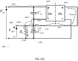
- FIGS. 1A), 1B ) and 1C are simplified electrical circuit diagrams 100a, 100b, 100c illustrating basic operational features of two different embodiments of resonant step-down DC-DC power converters in accordance with the present invention.
- the first embodiment is illustrated on FIGS. 1A) and 1B ) while the second embodiment is illustrated on FIG. 1C ).
- FIG. 1A shows a resonant step-down DC-DC power converter 100b comprising a primary side circuit and a secondary side circuit connected through a galvanic isolation barrier 107b.
- the primary side circuit comprises a positive input terminal 102b and a negative input terminal 101b for receipt of a DC or AC input voltage V in from an input voltage or power source (not shown).
- An input capacitor C in is electrically connected between the positive input terminal 102b and a negative input terminal 101b to form an energy reservoir for the input power or input voltage source.
- the primary side circuit additionally comprises an input side 106b of a resonant network arranged in front of a galvanic isolation barrier 107.
- the secondary side circuit comprises an output capacitor C out having a first electrode electrically connected to the converter output voltage V out at output terminal 104b.
- a second electrode of the output capacitor C out situated at a lower voltage potential than the first electrode, is connected to the positive input terminal 102b on the input side circuit via an electrical short-circuit connection or wire 109b extending across the galvanic isolation barrier 107b.
- the output capacitor C out and input capacitor C in are connected in series or cascade between the DC or AC input voltage V in , i.e. between positive and negative terminals of the input voltage or power source coupled to the output terminal 104b and the negative input terminal 101b, respectively.
- the presence of the electrical short-circuit connection 109b provides the conversion from an ordinary resonant isolated DC-DC power converter to the present resonant step-down DC-DC power converter which lacks galvanic isolation between the input side circuit and the output side circuit.
- the input voltage port of the original resonant isolated DC-DC power converter between the positive and negative terminals 102b, 101b i.e.
- the resonant step-down DC-DC power converter embodiments 100b, 100c may comprise permanently connected electrical short-circuit connections or wires 109b, 109c to provide a single mode of operation of the resonant DC-DC power converter in question with fixed voltage step-down functionality.
- the coupling or interconnection of the primary and secondary circuits of the power converters 100b, 100c through the electrical short-circuit connections 109b, 109c may be selectable or programmable such that each of the power converters 100b, 100c may possess two distinct and selectable modes of operation as discussed below in further detail with reference to FIGS. 1D) and 1E ).
- the skilled person will understand that the input and output capacitors C in and C out of the resonant step-down DC-DC power converter embodiments 100b, 100c may be formed exclusively by parasitic capacitances associated with the primary side circuit and the secondary side circuit, respectively.
- An electrical load R L of the step-down DC-DC converter 100b is coupled between the output terminal 104b and the positive input terminal 102b, which is across the output capacitor, such that these terminals form an output port of the DC-DC converter 100b.
- the primary side circuit comprises the previously discussed input side 106b of the resonant network of the step-down DC-DC converter 100b and the secondary side circuit comprises an output side 108b of the resonant network.
- the skilled person will appreciate that the resonant network may include numerous circuit topologies depending on the particular type of DC-DC converter in question.
- the resonant network preferably comprises at least one inductor for energy storage and release, but may alternatively exclusively comprise capacitors for energy storage.
- the resonant network is configured for alternatingly being charged from the input voltage V in and discharged to the output capacitor C out through the isolation barrier 107b in accordance with a switch control signal to produce the converter output voltage V out .
- the primary side circuit preferably comprises at least one semiconductor switch, for example a MOSFET, which is switched between on-states and off-states by the switch control signal such that the input voltage is modulated in accordance with a switch control signal.
- the frequency of the switch control signal of the semiconductor switch arrangement which excites the resonant network may be at or above 30 MHz to form a so-called VHF type of step-down DC-DC power converter.
- the switch control signal may comprise a PWM modulated control signal.
- the primary side circuit may comprise an inductor that is charged with energy during an on-state of the least one semiconductor switch from the input capacitor C in and/or the DC or AC input voltage V in .
- the inductor of the primary side circuit may subsequently be discharged through the output side 108b of the resonant network and the output capacitor C out in an off-state of the least one semiconductor switch.
- the secondary side circuit may comprise a diode based rectifier or a synchronous rectifier in front of the output capacitor to produce the converter output voltage V out as a DC output voltage.
- the electrical short-circuit connection or wire 109b eliminates the galvanic isolation between the primary and secondary side circuits of the resonant step-down DC-DC converter 100b by interconnecting the second electrode of the output capacitor C out and the positive input terminal 102b, it provides numerous new benefits to the DC-DC converter as a whole as illustrated with reference to FIG 1B ).
- the series connection of the output and input capacitors C out , C in means that the primary side circuit only needs to withstand the converter output voltage V out minus the input voltage across C in instead of the entire DC or AC input voltage V in delivered by the input voltage or power source which is the situation in the prior art isolated DC-DC converter topology.
- the reduced voltage across the primary side circuit reduces the required maximum voltage rating of active and passive components therein leading to physically smaller and/or less costly active and passive components for example inductors, capacitors (including C in ), transistors and diodes etc.
- active and passive components for example inductors, capacitors (including C in ), transistors and diodes etc.
- life span of the latter components may increase by the smaller voltage stress.
- the smaller amount of power to be transferred through the DC-DC converter 100b for supplying a given amount of power to the load R L of the converter leads to reduced power requirements for active semiconductors switches allowing less costly and physically smaller semiconductors to be applied.
- the first output current path I convert which shows how secondary side current charges the output capacitor C out and delivers output power to the load R L of the converter.
- the secondary side current comprises an AC component 113a and a DC component 113b such that the latter is dissipated in the load R L .
- the secondary side current delivers output power passing from the source of the DC or AC input voltage V in and through the resonant network to the output side circuit in a conventional manner.
- the present DC-DC converter 100b also comprises a second output current path delivering current or power directly from the DC or AC input voltage source to the output capacitor C out and the load R L without passing through the power converter 100b.
- This direct current comprises an AC current component delivered to the output capacitor C out as illustrated by AC input current path 111a and a DC current component delivered to the load R L as illustrated by DC input current path 111b.
- the AC current component 111a and the DC current component 111b of the input current path passes through the short-circuit connection 109b and through the positive and negative inputs of the primary side circuit 106b such that the DC current component 111b of the direct current remains unprocessed by the converter. Hence, this DC current component is supplied directly to the load R L without any noticeable power loss.
- the skilled person will appreciate that a practical electrical short circuit connection 109b will possess a certain DC resistance and an upper limit for this DC resistance will vary depending on input/output voltage and/or current requirements of the converter 100b.
- the electrical short-circuit connection may possess a DC resistance of less than 1 k ⁇ , even more preferably less than 100 ⁇ , such as less than 10 ⁇ .
- the electrical short circuit connection 109b may have a unidirectional resistance such that the DC resistance only falls below the above-mentioned upper limits in one direction and exhibits a much larger DC resistance in the opposite direction, i.e. a diode characteristic.
- the electrical short-circuit connection or wire 109c extending across the isolation barrier 107c is connecting the first positive electrode of the output capacitor C out to the negative input terminal 101c of the primary side circuit.
- a series coupling of the output capacitor C out and the input capacitor C in from the input voltage V in at the positive input terminal 102c to the negative electrode 103c of the output capacitor C out is established.
- the negative electrode 101c of the output capacitor C out is at a lower electric potential than the negative input terminal 101c. In this manner, the DC or AC input voltage V in to the power converter 100c is once again applied across the series connected input and output capacitors C in and C out .
- the converter load R L is coupled between the output terminal 104c and the terminal 103c which also is across the output capacitor. Otherwise, circuit functions, electrical component characteristics and component values of this second embodiment of resonant power converter 100c may be identical to those of the first embodiment of the resonant power converter 100b.
- FIG. 1D is a simplified electrical circuit diagram of a resonant step-down DC-DC power converter 100d in accordance with a third embodiment of the present the invention.
- a converter core 105d of the resonant power converter 100d may be identical to the core 105b of the resonant power converter 100c discussed above in connection with FIG. 1A) and 1B ).
- the present resonant power converter embodiment 100d comprises a mode selecting controllable semiconductor switch SW1 operating in conjunction with a rectifying element 111e such as a diode or an active semiconductor diode such as a controllable semiconductor switch.
- the operation of the resonant step-down DC-DC power converter 100d corresponds to the operation of the resonant step-down DC-DC power converter 100e discussed in detail below.
- FIG. 1E shows a simplified electrical circuit diagram of a resonant step-down DC-DC power converter 100e in accordance with a 4 th embodiment of the present the invention.
- a converter core 105e of the resonant power converter 100e may be identical to the core 105 of the resonant power converter 100c discussed above in connection with FIG. 1C ).
- the present resonant power converter embodiment 100e comprises a mode selecting controllable semiconductor switch SW1 operating in conjunction with a rectifying element 111e such as a diode or an active semiconductor diode such as a controllable semiconductor switch.
- the rectifying element 111e is inserted in a short-circuit connection or wire 109e which connects a negative input terminal 109e of the power converter to a first positive electrode of the output capacitor C out .
- the latter short-circuit connection corresponds to the short circuit connection 109c of the previously discussed resonant power converter 100c.
- the short-circuit wire 109e effectively places the output capacitor C out and input capacitor C in is series, albeit possibly with a minor diode voltage drop, between the input voltage V in terminals 104e, 103e of the resonant power converter 100e.
- the mode selecting controllable semiconductor switch SW1 is coupled between the negative input terminal 101e and the second negative electrode of the output capacitor 103e and configured to selectively break and close the electrical connection between these terminals 101e, 103e.
- the switch SW1 may comprise one or more BJT(s), FET(s) MOSFET(s) or IGBT(s) such as a Gallium Nitride (GaN) or Silicon Carbide (SiC) transistor.
- SW1 may be switched between a conducting or ON state and non-conducting or OFF state to connect and break, respectively, the electrical connection between terminals 101e, 103e by a suitable control voltage applied on a gate or base terminal of the switch SW1.
- a mode controlling circuit (not shown) integrated with or coupled to the present resonant power converter 100e may supply this control voltage to SW1.
- the mode selecting controllable semiconductor switch SW1 When the mode selecting controllable semiconductor switch SW1 is placed in the non-conducting or OFF state (as illustrated) the negative terminals of the C out and C in capacitors are disconnected and the rectifying element 111e forward biased. Hence, the input and output capacitors C out and C in are series connected through the rectifying element 111e.
- the rectifying element 111e is forward biased because the DC or AC input voltage V in is larger than the output voltage V out allowing the previously discussed input current of the power converter to flow directly through C in and into C out to charge the output capacitor.
- the resonant power converter 100e is placed in a first mode of operation where it largely functions as the resonant power converter 100c of FIG. 1C ) discussed above, i.e.
- the present resonant power converter embodiment 100e is switched to the second mode of operation.
- the rectifying element 111e is reversely biased and hence non-conducting due to the electrical connection between the negative capacitor terminals 101e, 103e.
- the above-discussed series connection (through the rectifying element 111e) of the input and output capacitors C out and C in in the first mode is broken or opened.
- the mode switching feature i.e. from the first mode to the second mode or vice versa, of the present resonant power converter 100e is accompanied with several advantages.
- the mode switching feature may be used to dynamically switch the present resonant power converter 100e between the first and second modes during operation of the converter 100e by appropriate control of the control terminal of SW1.
- the dynamic mode switching feature increases the input voltage range of the resonant power converter 100e.
- the DC input voltage range may be increased to 10 - 30 V by utilizing both the first mode and second mode of the resonant step-down DC-DC power converter during operation of the converter.
- the resonant step-down DC-DC power converter is switched dynamically between the first and second modes of operation in accordance with the input voltage waveform.
- the increase of DC input voltage range achieved by the dynamic mode switching feature is particular advantageous because resonant power converters generally suffer from a restricted or narrow DC input voltage range compared to non-resonant DC-DC power converters.
- Another advantage of the dynamic mode switching feature is an improved power factor (PF) of the resonant power converter 100e.
- the power factor of a switched mode power converter or supply is an important performance metric in numerous applications such as LED lamps where regulatory requirements for minimum power factor, such as larger than 0.9, may exist.
- the improved PF is achieved by the dynamic mode switching feature because this feature allows the converter to track AC variations of the input voltage to the converter such as the AC variations in the waveform of a rectified 50/60 Hz mains voltage.
- the flow of input current in the resonant step-down DC-DC power converter 100e in the first and second modes of operation is illustrated by a first DC input current path 111b1 and a second DC input current path 111b2.
- first mode of operation of the converter 100e i.e. the step-down functionality
- the input current flows through the first DC input current path 111b1 where DC input current flows through the diode 111e and through the converter load R L .
- the second mode of operation of the converter 100e is selected, i.e. SW1 is conducting and ordinary conversion functionality
- the input current flows through the second DC input current path 111b2 where the diode 111e is blocking and the DC input current flows through SW1 to the negative rail or terminal 103d of the converter without passing through the converter load.
- FIG. 1F is a simplified electrical circuit diagram of a first converter core 105f that may be utilized as converter core 105b, 105c, 105d, 105e of each of the step-down DC-DC power converter embodiments 100b, 100c, 100d, 100e, illustrated on FIGS. 1A), 1B ), 1C ), 1D) and 1E ), respectively.
- the first converter core 105f comprises a plurality of separate resonant DC-DC power converter cores 110f.
- Each of the separate resonant DC-DC power converter cores 110f comprises an input side 111 of a resonant network coupled to an output side 113 of the resonant network through a galvanic isolation barrier 107f.
- the input sides 111 of the resonant DC-DC power converter cores 110e may be connected in parallel or series.
- the output sides 113 of the resonant DC-DC power converter cores 110f may likewise be connected in parallel or series.
- the parallelization of the plurality of input sides 111 and/or the parallelization of the one or more output sides 113 increases the power rating of a step-up DC-DC power converter utilizing the first converter core 105f.
- each of the separate resonant DC-DC power converter cores 110f may comprise one of the prior art resonant DC-DC power converter cores discussed below with reference to FIGS. 2 , 3 and 4 .
- FIG. 1G is simplified electrical circuit diagram of a second converter core 105g that may be utilized as converter core 105b, 105c, 105d, 105e of each of the step-down DC-DC power converter embodiments 100b, 100c, 100d, 100e illustrated on FIGS. 1A), 1B ), 1C ), 1D) and 1E ), respectively.
- the second converter core 105g comprises a plurality of separate resonant power inverters 114g.
- Each of the separate resonant power inverter cores 114g comprises an input side 115 of a resonant network coupled to one or more rectifier(s) 117 of the resonant DC-DC power converter core 105g through a galvanic isolation barrier 107g.
- the separate resonant power inverter cores 114g may be connected in parallel or series. Likewise, the respective output side of the one or more rectifier(s) 117 may also be connected in series or parallel. However, galvanic isolation may be inserted between the one or more rectifier(s) 117 if these are coupled in series.
- FIG. 2A shows an electrical circuit diagram of a prior art isolated class E resonant DC-DC converter 200 comprising a series resonant network or circuit including inductor L 2 and capacitor C 1 .
- the prior art class E resonant converter comprises a primary side circuit and a secondary side circuit connected through a galvanic isolation barrier 207.
- the primary side circuit comprises a positive input terminal 202 and a negative input terminal 201 for receipt of a DC or AC input voltage V in from a voltage or power source (not shown).
- An input capacitor C in is electrically connected between the positive input terminal 202b and a negative input terminal 201 to form an energy reservoir for the voltage source.
- a converter core 205 comprises a resonant network which includes first and second series connected inductors L 1 and L 2 and a semiconductor switch arrangement comprising a MOSFET switch S (or another suitable type of semiconductor switch) with a drain terminal connected to a midpoint node between the L 1 and L 2 .
- the primary side circuit is arranged in front of an isolation barrier 207 formed by coupling capacitors C 1 and C 2 .
- the secondary side circuit comprises an output capacitor C out having a first electrode electrically connected to the converter output voltage V out at output terminal 204.
- a second negative electrode of the output capacitor C out is coupled to a negative terminal 203 of the converter output voltage.
- a load of the isolated class E resonant DC-DC converter 200 is schematically illustrated by load resistor R L and coupled between the positive and negative output terminals 204, 203.
- FIG. 2B is an electrical circuit diagram of a class E resonant step-down DC-DC power converter 200c comprising a series resonant circuit in accordance with a 7 th embodiment of the invention.
- the class E resonant step-down DC-DC power converter 200b may be obtained by conversion of the above-mentioned prior art isolated class E resonant DC-DC converter 200 by inserting or adding an electrical short circuit connection 209c extending across a galvanic isolation barrier 207c of the converter 200c.
- the galvanic isolation barrier 207c comprises series capacitors C 1 and C 2 .
- the electrical short circuit connection 209c electrically connects the negative input terminal 201c and the first positive electrode 204c of the output capacitor C out .
- the first positive electrode 204c is also connected to the converter output voltage V out .
- the electrical short-circuit connection or wire 209c effectively places the output capacitor C out and input capacitor C in in series or cascade across the DC or AC input voltage V in .
- the converter load schematically illustrated by the load resistor R L , is coupled in parallel across the output capacitor C out .
- the series capacitor C 2 of the galvanic isolation barrier 207c prevents DC current from flowing from the second negative electrode 203b of the output capacitor C out and back to the negative input terminal 201c. In this manner, the DC current is directed or forced through the electrical short circuit connection 209b and back through the input capacitor C in .
- the isolation barrier 207c is important for the operation of the present class E resonant step-down DC-DC power converter 200c as otherwise would nodes 201c and 203c and 204c be directly electrically connected causing a short circuit at the converter input.
- the series resonant network of the converter core 205c of the converter 200c may, in addition to the above-discussed first and second series connected inductors L 1 and L 2 , comprise a capacitor (C S ) arranged across drain and source terminals of the MOSFET switch S to increase a resonant current and/or adjust/fine-tune a resonance frequency of the power converter 200c.
- a yet further capacitor C D may be arranged across the rectifying diode D to adjust a duty cycle of the secondary part of the power converter 200c, i.e. the class E rectifier.
- the series resonant network is excited by the MOSFET switch S such that the series resonant network is alternatingly charged from the DC or AC input voltage V in and discharged to the output capacitor C out through the galvanic isolation barrier 207c and through a rectification circuit comprising inductance L 3 and diode D.
- FIG. 3A is an electrical circuit diagram of a prior art transformer isolated class E resonant DC-DC converter 300 comprising a series resonant circuit.
- a converter core 305 of the converter 300 comprises a series resonant circuit which at least inductors L 2 , L 3 and capacitors C S and C 1 .
- the prior art DC-DC converter 300 comprises a primary side circuit and a secondary side circuit connected through a galvanic isolation barrier 307 provided by the transformer 308.
- the primary side circuit comprises a positive input terminal 302 and a negative input terminal 301 for receipt of a DC or AC input voltage V in from a voltage or power source (not shown).
- An input capacitor C in is electrically connected between the positive input terminal 302 and a negative input terminal 301 to form an energy reservoir for the input voltage source.
- the primary side circuit additionally comprises a portion of a series resonant network or circuit which at least comprises inductors L 2 and capacitors C S and C 1 .
- a first inductor L 1 has a first end coupled to the positive input terminal 302 and a second end to a drain terminal of a MOSFET switch S which forms a switch arrangement of the present power converter 300.
- a secondary side circuit of the power converter 300 comprises an output capacitor C out having a first electrode electrically connected to the converter output voltage V out at output terminal 304.
- a second negative electrode of the output capacitor C out is coupled to a negative terminal 303 of the converter output voltage.
- An electrical or power converter load is schematically illustrated by load resistor R L and coupled between the positive and negative output terminals 304, 303 of the prior art DC-DC converter 300.
- the secondary side circuit furthermore comprises the third inductor L 3 connected across a secondary transformer winding of the above-mentioned transformer 308.
- the secondary transformer winding has a first end coupled to a cathode of rectifying diode D and a second end coupled to the positive electrode of the output capacitor C out .
- the rectifying diode D rectifies AC current generated by the secondary transformer winding and generates a DC voltage as the converter output voltage between the positive and negative output terminals 304, 303.
- An electrical or power converter load is schematically illustrated by load resistor R L coupled between the positive and negative output terminals 304, 303.
- FIG. 4A is an electrical circuit diagram of a prior art isolated single-ended primary-inductor converter (SEPIC) 400.
- SEPIC 400 comprises a primary side circuit and a secondary side circuit connected through a galvanic isolation barrier 407.
- the primary side circuit comprises a positive input terminal 402 and a negative input terminal 401 for receipt of a DC or AC input voltage V in from a voltage or power source (not shown).
- An input capacitor C in is electrically connected between the positive input terminal 402 and a negative input terminal 401 to form an energy reservoir for the input voltage source.
- a converter core 405 of the converter 400 comprises a series resonant circuit which includes a first inductor L 1 having first node coupled to the DC or AC input voltage V in and a second node coupled to a drain terminal of a MOSFET switch S.
- a source terminal of a MOSFET switch S of a switch arrangement is coupled to the negative input terminal 401.
- the prior art SEPIC 400 is a resonant type of power converter wherein a resonance frequency of the converter is determined by the resonant network of the converter core 405 comprising the first and second inductors L 1 , L 2 and the capacitors C S and C D .
- the primary side circuit is arranged in front of a galvanic isolation barrier 407 within the converter core 405 and formed by coupling capacitors C 1 and C 2 .
- the secondary side circuit comprises an output capacitor C out having a first electrode electrically connected to the converter output voltage V out at a positive output terminal 404.
- a second negative electrode of the output capacitor C out is coupled to a negative terminal 403 of the converter output voltage.
- a rectifying diode D rectifies AC current generated by a second inductor L 2 and charges the output capacitor C out such that the converter output voltage V out between the positive and negative output terminals 404, 403 is a DC voltage.
- a converter load of the SEPIC 400 illustrated by load resistor R L , is coupled between the positive and negative output terminals 404, 403.
- FIG. 4B is an electrical circuit diagram of a SEPIC 400c in accordance with a 9 th embodiment of the invention.
- the SEPIC 400c may be obtained by conversion of the above-mentioned prior art SEPIC 400 by inserting or adding an electrical short circuit connection 409c extending across a galvanic isolation barrier 407c of the SEPIC 400c.
- the galvanic isolation barrier 407c comprises series capacitors C 1 and C 2 which prevent the flow of DC current between the secondary side circuit and the primary side circuit in the isolated SEPIC 400 discussed above.
- the electrical short circuit connection 409c electrically connects the negative input terminal 401c and the positive electrode 404c of the output capacitor C out . As discussed in connection with FIGS.
- the electrical short-circuit connection or wire 409c effectively places the output capacitor C out and input capacitor C in is series or cascade across the positive and negative connections to the DC or AC input voltage V in such that the galvanic isolation between the primary and secondary side circuits is bypassed or eliminated.
- the electrical or power converter load schematically illustrated by the load resistor R L , is coupled between the converter output voltage V out at the output terminal 404c and the negative electrode 403c of the output capacitor.
- the series capacitor C 2 of the galvanic isolation barrier 407b prevents DC current from flowing from the second negative electrode 403b of the output capacitor C out and directly back to the negative input terminal 401b of the primary side circuit.
- the SEPIC 400c comprises a converter core 405c comprises a resonant network as discussed above comprising first and second inductors L 1 , L 2 and capacitors C S and C D .
- the series resonant network is excited by the MOSFET switch S such that the series resonant network is alternatingly charged from the DC or AC input voltage V in and discharged to the output capacitor C out through the galvanic isolation barrier 407c and through a rectification circuit comprising a rectifying diode D.
- the capacitor C S connected or arranged across drain and source terminals of the MOSFET switch S is optional, but may be helpful to increase a resonant current and/or adjust/fine-tune a resonance frequency of the resonant network SEPIC 400c.
- the capacitor C S may be formed exclusively by a parasitic capacitance of the MOSFET S.
- the optional capacitor C D may be arranged across the rectifying diode D to adjust a duty cycle of the power converter 400c.
Landscapes
- Engineering & Computer Science (AREA)
- Power Engineering (AREA)
- Dc-Dc Converters (AREA)
- Circuit Arrangement For Electric Light Sources In General (AREA)
Claims (14)
- Convertisseur CC/CC abaisseur à résonance (100b, 100c) comprenant :un circuit combinant primaire (106b, 106c) et un circuit combinant secondaire (108b, 108c) couplés par le biais d'une barrière d'isolation galvanique basée sur condensateur (107b, 107c),le circuit combinant primaire (106b, 106c) comprenant une borne d'entrée positive (102b, 102c) et une borne d'entrée négative (101b, 101c) pour la réception d'une tension d'entrée (Vin) et un condensateur d'entrée (Cin) couplé entre les bornes d'entrée positive et négative,le circuit combinant secondaire (108b, 108c) comprenant un condensateur de sortie (Cout) pouvant être chargé à une tension de sortie de convertisseur (Vout) entre une première électrode positive et une seconde électrode négative (103b, 103c) du condensateur de sortie (Cout),un réseau résonant configuré pour être, de manière alternée, chargé à partir de la tension d'entrée (Vin) et déchargé vers le condensateur de sortie (Cout) par le biais de la barrière d'isolation galvanique (107b, 107c) par un agencement de commutation semi-conducteur en fonction d'un signal de commande de commutation pour produire la tension de sortie du convertisseur, le signal de commande de commutation ayant une fréquence à 20 MHz ou plus,une connexion de court-circuit électrique (109b, 109c) sur la barrière d'isolation galvanique (107b, 107c) connectant, dans un premier cas, la seconde électrode négative (103b, 103c) du condensateur de sortie (Cout) à la borne d'entrée positive (102b, 102c) du circuit combinant primaire ou, dans un second cas, connectant la première électrode positive du condensateur de sortie (Cout) à la borne d'entrée négative (101b, 101c) du circuit combinant primaire (106b), établissant ainsi, à la fois dans le premier et le second cas, un couplage en série du condensateur de sortie (Cout) et du condensateur d'entrée (Cin),une connexion de charge, dans le premier cas, entre la première électrode positive (104b, 104c) du condensateur de sortie (Cout) et la borne d'entrée positive (101b, 101c) ou, dans le second cas, entre la seconde électrode négative (103b, 103c) du condensateur de sortie et la borne d'entrée négative (101b, 101c).
- Convertisseur CC/CC abaisseur à résonance (100b, 100c) selon la revendication 1, dans lequel la barrière d'isolation galvanique basée sur condensateur comprend :un premier condensateur (C1) couplé en série avec la borne d'entrée positive (102b, 102c) du circuit combinant primaire (106b, 106c) et la première électrode positive (104b, 104c) du condensateur de sortie (Cout) ; etun second condensateur (C2) couplé en série avec la borne d'entrée négative (101b, 101c) du circuit combinant primaire (106b, 106c) et la seconde électrode négative (103b, 103c) du condensateur de sortie (Cout).
- Convertisseur CC/CC abaisseur à résonance (100b, 100c) selon la revendication 2, dans lequel une capacité de chacun des premier et second condensateurs (C1, C2) est inférieure à 100 nF.
- Convertisseur CC/CC abaisseur à résonance (100b, 100c) selon la revendication 3, dans lequel chacun des premier et second condensateurs (C1, C2) comprend un condensateur céramique montable en surface SMD.
- Convertisseur CC/CC abaisseur à résonance (100b, 100c) selon l'une quelconque des revendications précédentes, dans lequel une résistance CC de la connexion de court-circuit électrique (109b, 109c) est inférieure à 1 kΩ.
- Convertisseur CC/CC abaisseur à résonance (100b, 100c) selon l'une quelconque des revendications précédentes, dans lequel le réseau résonant comprend :des premier et second inducteurs connectés en série connectés en série avec la borne de tension d'entrée positive (102b, 102c),un commutateur à semi-conducteur (S) ayant un premier noeud de commutation connecté entre un noeud de point intermédiaire entre les premier et second inducteurs connectés en série (L1, L2), un second noeud de commutation connecté à la borne d'entrée négative (101b, 101c) du circuit combinant primaire (106b, 106c) et une borne de commande connectée au terminal de commande de commutation ; etun circuit redresseur connecté entre les premier et second condensateurs de la barrière d'isolation galvanique et la première électrode positive (104b, 104c) et la seconde électrode négative (103b, 103c) du condensateur de sortie (Cout).
- Convertisseur CC/CC abaisseur à résonance (100b, 100c) selon l'une quelconque des revendications précédentes, dans lequel l'agencement de commutation semi-conducteur comprend un ou plusieurs commutateurs à semi-conducteurs (S) contrôlables.
- Convertisseur CC/CC abaisseur à résonance (100b, 100c) selon la revendication 7, dans lequel le(s) commutateur(s) à semi-conducteur (S) contrôlable(s) est/sont configuré(s) pour une commutation à tension nulle et/ou une commutation à courant nul.
- Convertisseur CC/CC abaisseur à résonance (100b, 100c) selon l'une quelconque des revendications précédentes, comprenant en outre :un élément redresseur (111d, 111e) tel qu'une diode configuré pour :conduire, dans le premier cas, un courant de la borne d'entrée positive (102b, 102c) à la seconde électrode négative (103b, 103c) du condensateur de sortie (Cout),conduire, dans le second cas, un courant de la borne d'entrée négative (101e) à la première électrode positive (104d) du condensateur de sortie ; etun commutateur à semi-conducteur de sélection de mode (SW1) configuré pour interrompre et fermer sélectivement, dans le premier cas, une connexion électrique entre la borne d'entrée positive (102b, 102c) et la première électrode positive (104b, 104c) du condensateur de sortie (Cout) et interrompre et fermer sélectivement, dans le second cas, une connexion électrique entre la borne d'entrée négative (101b, 101c) et la seconde électrode négative (103b, 103c) du condensateur de sortie, de telle sorte à :établir, dans un premier mode du convertisseur CC/CC abaisseur à résonance, la connexion en série du condensateur de sortie (Cout) et du condensateur d'entrée (Cin) par le biais de l'élément redresseur (111d, 111e) ; etouvrir ou interrompre, dans un second mode du convertisseur CC/CC abaisseur à résonance, le couplage en série du condensateur de sortie (Cout) et du condensateur d'entrée (Cin).
- Procédé de conversion d'un convertisseur CC/CC isolé à résonance ayant une fréquence de commutation à 20 MHz ou plus en un convertisseur CC/CC abaisseur non isolé à résonance (100b, 100c) possédant une efficacité de conversion de courant plus élevée, ledit procédé comprenant les étapes suivantes :a) fourniture d'un circuit combinant primaire (106b, 106c) et d'un circuit combinant secondaire (108b, 108c) du convertisseur CC/CC isolé,b) couplage éventuel d'un condensateur d'entrée (Cin) entre une borne d'entrée positive et une borne d'entrée négative du circuit combinant primaire (106b, 106c),c) couplage éventuel d'une électrode positive d'un condensateur de sortie (Cout) à une borne de sortie positive du circuit combinant secondaire (108b, 108c) et couplage éventuel d'une électrode négative du condensateur de sortie (Cout) à une borne de sortie négative (103b, 103c) du circuit combinant secondaire,d) fourniture du couplage électrique du circuit combinant primaire et du circuit combinant secondaire (108b, 108c) par le biais d'une barrière d'isolation galvanique basée sur condensateur (107b, 107c),e) fourniture d'un réseau résonant configuré pour être en alternance chargé à partir d'une tension d'entrée (Vin) du convertisseur et déchargé vers le condensateur de sortie (Cout) par le biais de la barrière d'isolation galvanique (107b, 107c) selon un signal de commande de commutation pour produire une tension de sortie du convertisseur,f) connexion, dans un premier cas, d'un court-circuit électrique (109b, 109c) par le biais de la barrière d'isolation galvanique basée sur condensateur (107b, 107c) de la borne de sortie négative (103b, 103c) du circuit combinant secondaire à la borne d'entrée positive (102b, 102c) du circuit combinant primaire ou connexion, dans un second cas, de la borne de sortie positive (104b, 104c) du circuit combinant secondaire (108b, 108c) à la borne d'entrée négative du circuit combinant primaire (106b, 106c), établissant ainsi à la fois dans le premier cas et le second cas, un couplage en série du condensateur de sortie (Cout) et du condensateur d'entrée (Cin),g) couplage, dans un premier cas, d'une charge de convertisseur de courant (RL) entre la borne positive (104b, 104c) du circuit combinant secondaire (108b, 108c) et la borne d'entrée positive (102b, 102c) ou couplage, dans le second cas, de la charge de convertisseur de courant (RL) entre la borne de sortie négative (103b, 103c) du circuit combinant secondaire (108b, 108c) et la borne d'entrée négative (101b, 101c) du circuit combinant primaire.
- Procédé de conversion d'un convertisseur CC/CC isolé selon la revendication 10, comprenant une autre étape de :h) connexion électrique, dans le premier cas, d'une source de tension d'entrée entre la borne d'entrée négative (101b, 101c) du circuit combinant primaire (106b, 106c) et la borne de sortie positive (104b, 104c) du circuit combinant secondaire (108b, 108c), oui) connexion électrique, dans le second cas, d'une source de tension d'entrée entre la borne d'entrée positive (102b, 102c) du circuit combinant primaire (106b, 106c) et la borne de sortie négative (103b, 103c) du circuit combinant secondaire (108b, 108c).
- Procédé de conversion d'un convertisseur CC/CC isolé selon la revendication 10 ou 11, comprenant les étapes suivantes :j) insertion d'un élément redresseur (111d, 111e) dans la connexion de court-circuit électrique,k) insertion d'un commutateur à semi-conducteur de sélection de mode (SW1), dans le premier cas, entre la borne d'entrée positive (102b, 102c) et la première électrode positive (104b, 104c) du condensateur de sortie et dans le second cas, entre la borne d'entrée négative (101b, 101c) et la seconde électrode négative (103b, 103c) du condensateur de sortie.
- Ensemble d'éclairage à DEL comprenant :un convertisseur CC/CC abaisseur à résonance (100b, 100c) selon l'une quelconque des revendications 1 à 9 monté sur une carte de circuit imprimé de l'ensemble,une entrée de tension de secteur alternatif CA connectée à une entrée d'un redresseur de secteur,une sortie du redresseur de secteur connectée, dans le premier cas, entre la première électrode positive (104b, 104c) du condensateur de sortie (Cout) et l'électrode d'entrée négative (101b, 101c) ou connectée, dans le second cas, entre la borne d'entrée négative (101b, 101c) et l'électrode négative (103b, 103c) du condensateur de sortie (Cout) pour fournir une tension de secteur redressée au convertisseur CC/CC abaisseur à résonance dans les deux cas.
- Lampe à DEL comprenant un ensemble d'éclairage à DEL selon la revendication 13.
Priority Applications (1)
| Application Number | Priority Date | Filing Date | Title |
|---|---|---|---|
| EP15702981.0A EP3097635B1 (fr) | 2014-01-22 | 2015-01-20 | Convertisseur de puissance cc-cc abaisseur |
Applications Claiming Priority (3)
| Application Number | Priority Date | Filing Date | Title |
|---|---|---|---|
| EP14152070 | 2014-01-22 | ||
| EP15702981.0A EP3097635B1 (fr) | 2014-01-22 | 2015-01-20 | Convertisseur de puissance cc-cc abaisseur |
| PCT/EP2015/051007 WO2015110427A1 (fr) | 2014-01-22 | 2015-01-20 | Convertisseurs abaisseurs de courant continu/courant continu à résonance |
Publications (2)
| Publication Number | Publication Date |
|---|---|
| EP3097635A1 EP3097635A1 (fr) | 2016-11-30 |
| EP3097635B1 true EP3097635B1 (fr) | 2018-03-14 |
Family
ID=49956077
Family Applications (1)
| Application Number | Title | Priority Date | Filing Date |
|---|---|---|---|
| EP15702981.0A Active EP3097635B1 (fr) | 2014-01-22 | 2015-01-20 | Convertisseur de puissance cc-cc abaisseur |
Country Status (11)
| Country | Link |
|---|---|
| US (1) | US10340805B2 (fr) |
| EP (1) | EP3097635B1 (fr) |
| JP (1) | JP6473756B2 (fr) |
| KR (1) | KR20160111468A (fr) |
| CN (1) | CN105934876B (fr) |
| CA (1) | CA2935004A1 (fr) |
| ES (1) | ES2671123T3 (fr) |
| MX (1) | MX354807B (fr) |
| TW (1) | TWI670921B (fr) |
| UA (1) | UA117689C2 (fr) |
| WO (1) | WO2015110427A1 (fr) |
Families Citing this family (46)
| Publication number | Priority date | Publication date | Assignee | Title |
|---|---|---|---|---|
| US10063284B2 (en) * | 2014-03-04 | 2018-08-28 | Triune Ip Llc | Isolation for communication and power |
| EP3024133A1 (fr) * | 2014-11-24 | 2016-05-25 | Broadband Power Solutions | Convertisseur d'alimentation CC/CA |
| JP6168254B2 (ja) * | 2015-02-26 | 2017-07-26 | 株式会社村田製作所 | 電圧検出回路、送電装置および電力伝送システム |
| JP6477220B2 (ja) * | 2015-05-12 | 2019-03-06 | Tdk株式会社 | 共振コンバータおよびスイッチング電源装置 |
| WO2016202895A1 (fr) * | 2015-06-16 | 2016-12-22 | Npc Tech Aps | Ensemble convertisseur de puissance résonant galvaniquement isolé |
| FR3040839B1 (fr) * | 2015-09-04 | 2019-10-25 | Commissariat A L'energie Atomique Et Aux Energies Alternatives | Convertisseur electronique et systeme d'eclairage comprenant un tel convertisseur |
| FR3041190B1 (fr) * | 2015-09-16 | 2018-11-09 | Valeo Equipements Electriques Moteur | Procede et dispositif d'alimentation d'un circuit electronique dans un vehicule automobile, et module de controle electronique correspondant |
| KR20230107913A (ko) | 2016-06-15 | 2023-07-18 | 와틀로 일렉트릭 매뉴팩츄어링 컴파니 | 열시스템용 전력 변환기 |
| US10298132B2 (en) * | 2016-10-13 | 2019-05-21 | Intersil Americas LLC | Switching power supply for low step down conversion ratio with reduced switching losses |
| CN106452108A (zh) * | 2016-11-04 | 2017-02-22 | 南京航空航天大学 | 基于ClassE变换器的超高频整流变换电路及其阻抗匹配方法 |
| FR3060904B1 (fr) * | 2016-12-15 | 2023-10-27 | 3D Plus | Convertisseur de tension haute frequence continue de type buck quasi-resonant |
| EP3656046A1 (fr) | 2017-07-17 | 2020-05-27 | NPC Tech ApS | Convertisseur de puissance cc-cc à résolution de courant de sortie améliorée |
| CN107276393B (zh) * | 2017-07-25 | 2023-10-20 | 广州金升阳科技有限公司 | 一种高压电源电路 |
| US10917001B2 (en) * | 2017-08-21 | 2021-02-09 | Flex Ltd. | Adaptive resonant frequency converter |
| CN107689691B (zh) * | 2017-09-26 | 2019-11-12 | 广州大学 | 一种磁共振式无线充电传感器网络节点设计方法 |
| US10224803B1 (en) * | 2017-12-20 | 2019-03-05 | Infineon Technologies Austria Ag | Switched capacitor converter with compensation inductor |
| KR102098020B1 (ko) * | 2017-12-22 | 2020-04-07 | 주식회사 포스코 | 커패시터 커플링 구조를 갖는 직류 전압 제어 장치 |
| CN108322054A (zh) * | 2018-03-09 | 2018-07-24 | 南京理工大学 | 降低二极管电压应力的软开关谐振直流变换器及计算方法 |
| CN108736710B (zh) * | 2018-07-06 | 2024-04-12 | 武汉普天洲际宜通电源有限公司 | 一种dc-dc功率变换电路 |
| US10594205B2 (en) * | 2018-08-01 | 2020-03-17 | Newvastek Co., Ltd. | High-frequency half-wave rectifier system of low-harmonicity and high-efficiency |
| NL2021926B1 (en) * | 2018-11-02 | 2020-05-14 | Prodrive Tech Bv | Electrical power converter |
| CN111525802B (zh) * | 2019-02-01 | 2021-08-06 | 台达电子工业股份有限公司 | 变换装置 |
| CN111525803B (zh) | 2019-02-01 | 2021-10-26 | 台达电子工业股份有限公司 | 变换装置 |
| DE102019103730B4 (de) * | 2019-02-14 | 2021-02-04 | Infineon Technologies Austria Ag | Schaltungsanordnung mit galvanischer isolation zwischen elektronischen schaltungen |
| CN110061622B (zh) * | 2019-03-19 | 2023-10-27 | 华东师范大学 | 一种非隔离式多路程控可调正负直流电压供电装置 |
| KR102596082B1 (ko) * | 2019-05-14 | 2023-10-31 | 광동 오포 모바일 텔레커뮤니케이션즈 코포레이션 리미티드 | 강압 회로, 전자 장치 및 강압 방법 |
| IT201900007974A1 (it) * | 2019-06-04 | 2020-12-04 | Eggtronic Eng S P A | Convertitore per trasferire potenza elettrica ad un carico elettrico |
| WO2020096655A1 (fr) | 2019-06-26 | 2020-05-14 | Huawei Technologies Co., Ltd. | Système de conversion de puissance bidirectionnel à ports multiples et procédé associé |
| US11973414B2 (en) * | 2020-01-31 | 2024-04-30 | Schneider Electric It Corporation | Decoupled PCB structure to parallel power transistors |
| CN113258755B (zh) * | 2020-02-13 | 2022-07-26 | 宏碁股份有限公司 | 升压转换器 |
| TWI715464B (zh) * | 2020-03-17 | 2021-01-01 | 宏碁股份有限公司 | 降壓轉換器 |
| CN113691134B (zh) * | 2020-05-19 | 2023-10-27 | 台达电子工业股份有限公司 | 电源转换装置及电源供应系统 |
| WO2021257680A1 (fr) * | 2020-06-16 | 2021-12-23 | North Carolina State University | Dispositif d'alimentation électrique à pilote de grille isolé et applications associées |
| CN113904554A (zh) | 2020-07-06 | 2022-01-07 | 台达电子工业股份有限公司 | 直流/直流电源转换器 |
| CN113904563A (zh) | 2020-07-06 | 2022-01-07 | 台达电子工业股份有限公司 | 电源转换模块 |
| CN111817572B (zh) * | 2020-07-20 | 2022-02-25 | 厦门大学 | 一种实现部分功率变换的多端口直流系统 |
| MX2023001715A (es) | 2020-08-10 | 2023-05-18 | Terminal Power LLC | Módulo autoconvertidor de cc-cc. |
| IT202100002360A1 (it) * | 2021-02-03 | 2022-08-03 | Eggtronic Eng S P A | Convertitore per trasferire potenza elettrica ad un carico elettrico |
| JP7387663B2 (ja) * | 2021-03-02 | 2023-11-28 | 株式会社東芝 | 電力変換回路及び電力変換装置 |
| KR102709644B1 (ko) | 2021-11-26 | 2024-09-25 | 주식회사 뉴파워 프라즈마 | 강압형 dc/dc 컨버터 및 그 제어 방법 |
| EP4398472A1 (fr) * | 2021-12-27 | 2024-07-10 | Samsung Electronics Co., Ltd. | Dispositif et procédé d'émission de tension de taille constante dans un système de communication sans fil |
| CN114285275B (zh) * | 2021-12-27 | 2023-10-31 | 阳光电源股份有限公司 | 一种电源变换系统及供电系统 |
| US11742752B2 (en) * | 2022-01-21 | 2023-08-29 | Inventronics Gmbh | DC-DC converter having two resonant circuits and method for control and operation of a DC-DC converter |
| CN114845443B (zh) * | 2022-07-04 | 2022-09-20 | 江苏南通二建集团讯腾云创智能科技有限公司 | 基于工业数据的厂房照明设备的能耗优化方法 |
| CN117175943B (zh) * | 2023-08-10 | 2024-09-17 | 哈尔滨工业大学 | 一种新型负压输出软开关高降压比变换器及拓扑结构 |
| CN117665382B (zh) * | 2024-01-31 | 2024-04-05 | 季华实验室 | 一种功率检测电路及功率检测pcb板 |
Family Cites Families (20)
| Publication number | Priority date | Publication date | Assignee | Title |
|---|---|---|---|---|
| JPH0464461A (ja) | 1990-07-04 | 1992-02-28 | Fuji Xerox Co Ltd | イオン流制御記録装置 |
| JPH04285468A (ja) | 1991-03-12 | 1992-10-09 | Fujitsu Ltd | スイッチングレギュレ−タ |
| JP2677075B2 (ja) * | 1991-08-30 | 1997-11-17 | 富士電機株式会社 | ハーフブリッジ形電力変換回路 |
| US5770911A (en) * | 1996-01-30 | 1998-06-23 | Cheng; Kan | Resonant thermoelectric generator |
| JP3219726B2 (ja) | 1996-12-13 | 2001-10-15 | 東光株式会社 | スイッチング電源装置 |
| US7768371B2 (en) * | 1998-02-05 | 2010-08-03 | City University Of Hong Kong | Coreless printed-circuit-board (PCB) transformers and operating techniques therefor |
| JP2001345189A (ja) | 2000-06-06 | 2001-12-14 | Energymate Co Ltd | 照明灯制御システム及びその制御方法 |
| US6987678B2 (en) * | 2002-10-23 | 2006-01-17 | International Rectifier Corporation | Switching voltage regulator for switch mode power supply with planar transformer |
| US6989997B2 (en) | 2003-06-25 | 2006-01-24 | Virginia Tech Intellectual Properties, Inc. | Quasi-resonant DC-DC converters with reduced body diode loss |
| JP5169039B2 (ja) * | 2007-06-29 | 2013-03-27 | Nec東芝スペースシステム株式会社 | Dc‐dcコンバータ |
| US8798409B2 (en) | 2010-10-07 | 2014-08-05 | Alcatel Lucent | Optical transmitter with flip-chip mounted laser or integrated arrayed waveguide grating wavelenth division multiplexer |
| US8810208B2 (en) | 2011-03-10 | 2014-08-19 | Tesla Motors, Inc. | Charging efficiency using selectable isolation |
| US8749995B2 (en) * | 2011-03-29 | 2014-06-10 | Texas Instruments Incorporated | Single-pulse resonant gate driver for driving switches in resonant isolated converters and other systems |
| CN102158096B (zh) | 2011-05-11 | 2013-11-20 | 南京博兰得电子科技有限公司 | 一种非隔离式谐振变换器 |
| US20130049918A1 (en) * | 2011-08-25 | 2013-02-28 | Futurewei Technologies, Inc. | Common Mode Choke Apparatus and Method |
| US9602018B2 (en) * | 2012-03-20 | 2017-03-21 | Infineon Technologies Austria Ag | Power converter with reduced power consumption in standby mode |
| US9439249B2 (en) * | 2013-01-24 | 2016-09-06 | Cree, Inc. | LED lighting apparatus for use with AC-output lighting ballasts |
| US9178422B2 (en) * | 2013-02-21 | 2015-11-03 | Texas Instruments Incorporated | Resonance-based single inductor output-driven DC-DC converter and method |
| US9871499B2 (en) * | 2013-03-15 | 2018-01-16 | Qorvo Us, Inc. | Multi-band impedance tuners using weakly-coupled LC resonators |
| US9564823B2 (en) * | 2014-10-01 | 2017-02-07 | Toyota Motor Engineering & Manufacturing North America, Inc. | DC-DC power conversion circuit with magnetic and capacitive isolation |
-
2015
- 2015-01-20 JP JP2016541225A patent/JP6473756B2/ja active Active
- 2015-01-20 ES ES15702981.0T patent/ES2671123T3/es active Active
- 2015-01-20 CN CN201580005400.4A patent/CN105934876B/zh active Active
- 2015-01-20 US US15/103,819 patent/US10340805B2/en active Active
- 2015-01-20 KR KR1020167022640A patent/KR20160111468A/ko not_active Application Discontinuation
- 2015-01-20 EP EP15702981.0A patent/EP3097635B1/fr active Active
- 2015-01-20 MX MX2016009422A patent/MX354807B/es active IP Right Grant
- 2015-01-20 CA CA2935004A patent/CA2935004A1/fr not_active Abandoned
- 2015-01-20 UA UAA201607048A patent/UA117689C2/uk unknown
- 2015-01-20 WO PCT/EP2015/051007 patent/WO2015110427A1/fr active Application Filing
- 2015-01-21 TW TW104101973A patent/TWI670921B/zh active
Also Published As
| Publication number | Publication date |
|---|---|
| CN105934876B (zh) | 2019-04-12 |
| EP3097635A1 (fr) | 2016-11-30 |
| TWI670921B (zh) | 2019-09-01 |
| MX354807B (es) | 2018-03-22 |
| CN105934876A (zh) | 2016-09-07 |
| TW201537879A (zh) | 2015-10-01 |
| KR20160111468A (ko) | 2016-09-26 |
| WO2015110427A1 (fr) | 2015-07-30 |
| US10340805B2 (en) | 2019-07-02 |
| CA2935004A1 (fr) | 2015-07-30 |
| UA117689C2 (uk) | 2018-09-10 |
| ES2671123T3 (es) | 2018-06-05 |
| JP6473756B2 (ja) | 2019-02-20 |
| JP2017505596A (ja) | 2017-02-16 |
| MX2016009422A (es) | 2016-09-16 |
| US20160322910A1 (en) | 2016-11-03 |
Similar Documents
| Publication | Publication Date | Title |
|---|---|---|
| EP3097635B1 (fr) | Convertisseur de puissance cc-cc abaisseur | |
| US10181798B2 (en) | Step-up DC-DC power converter | |
| RU2672260C2 (ru) | Резонансный dc-dc преобразователь мощности с управлением включением и выключением | |
| CN203691238U (zh) | 电子变换器以及相关照明系统 | |
| US9071161B2 (en) | Single stage PFC power supply | |
| JP4152745B2 (ja) | 多レベル入力ラインの力率修正用の切り換え可能な電力変換装置 | |
| US9130472B2 (en) | High efficient single switch single stage power factor correction power supply | |
| US7184287B2 (en) | Rectifier clamping circuit with reverse energy recovery | |
| Chub et al. | Single-switch galvanically isolated quasi-Z-source DC-DC converter | |
| JP6509381B2 (ja) | Dc‐dcコンバータ | |
| KR101092218B1 (ko) | 간단한 구조의 전류원을 이용한 led 구동회로 | |
| JP4577030B2 (ja) | スイッチング電源装置 | |
| TWI551025B (zh) | Lighting power conversion device | |
| JP2006211878A (ja) | スイッチング電源装置 | |
| US11817795B2 (en) | Switching power supply circuit | |
| JP5551995B2 (ja) | 電源装置及びこの電源装置を備えた照明装置 | |
| CN109256966B (zh) | 交流-直流功率变换器 | |
| KR102142630B1 (ko) | 전압구동형 동기정류기 구동회로 | |
| KR101656021B1 (ko) | 직렬공진형 컨버터 | |
| WO2007078158A1 (fr) | Survolteur-devolteur isole | |
| US10158284B2 (en) | PFC with stacked half-bridges on DC side of rectifier | |
| Ongaro et al. | ZVS isolated active clamp sepic converter for high power LED applications | |
| JP2005020948A (ja) | Dc−dcコンバータ | |
| JP2005102400A (ja) | 高周波インバータ装置および放電ランプ点灯装置 |
Legal Events
| Date | Code | Title | Description |
|---|---|---|---|
| PUAI | Public reference made under article 153(3) epc to a published international application that has entered the european phase |
Free format text: ORIGINAL CODE: 0009012 |
|
| 17P | Request for examination filed |
Effective date: 20160622 |
|
| AK | Designated contracting states |
Kind code of ref document: A1 Designated state(s): AL AT BE BG CH CY CZ DE DK EE ES FI FR GB GR HR HU IE IS IT LI LT LU LV MC MK MT NL NO PL PT RO RS SE SI SK SM TR |
|
| AX | Request for extension of the european patent |
Extension state: BA ME |
|
| DAX | Request for extension of the european patent (deleted) | ||
| GRAP | Despatch of communication of intention to grant a patent |
Free format text: ORIGINAL CODE: EPIDOSNIGR1 |
|
| STAA | Information on the status of an ep patent application or granted ep patent |
Free format text: STATUS: GRANT OF PATENT IS INTENDED |
|
| INTG | Intention to grant announced |
Effective date: 20170922 |
|
| GRAS | Grant fee paid |
Free format text: ORIGINAL CODE: EPIDOSNIGR3 |
|
| GRAA | (expected) grant |
Free format text: ORIGINAL CODE: 0009210 |
|
| STAA | Information on the status of an ep patent application or granted ep patent |
Free format text: STATUS: THE PATENT HAS BEEN GRANTED |
|
| AK | Designated contracting states |
Kind code of ref document: B1 Designated state(s): AL AT BE BG CH CY CZ DE DK EE ES FI FR GB GR HR HU IE IS IT LI LT LU LV MC MK MT NL NO PL PT RO RS SE SI SK SM TR |
|
| REG | Reference to a national code |
Ref country code: GB Ref legal event code: FG4D |
|
| REG | Reference to a national code |
Ref country code: CH Ref legal event code: EP Ref country code: AT Ref legal event code: REF Ref document number: 979770 Country of ref document: AT Kind code of ref document: T Effective date: 20180315 |
|
| REG | Reference to a national code |
Ref country code: IE Ref legal event code: FG4D |
|
| REG | Reference to a national code |
Ref country code: DE Ref legal event code: R096 Ref document number: 602015008790 Country of ref document: DE |
|
| REG | Reference to a national code |
Ref country code: ES Ref legal event code: FG2A Ref document number: 2671123 Country of ref document: ES Kind code of ref document: T3 Effective date: 20180605 |
|
| REG | Reference to a national code |
Ref country code: NL Ref legal event code: FP |
|
| REG | Reference to a national code |
Ref country code: LT Ref legal event code: MG4D |
|
| PG25 | Lapsed in a contracting state [announced via postgrant information from national office to epo] |
Ref country code: HR Free format text: LAPSE BECAUSE OF FAILURE TO SUBMIT A TRANSLATION OF THE DESCRIPTION OR TO PAY THE FEE WITHIN THE PRESCRIBED TIME-LIMIT Effective date: 20180314 Ref country code: LT Free format text: LAPSE BECAUSE OF FAILURE TO SUBMIT A TRANSLATION OF THE DESCRIPTION OR TO PAY THE FEE WITHIN THE PRESCRIBED TIME-LIMIT Effective date: 20180314 Ref country code: FI Free format text: LAPSE BECAUSE OF FAILURE TO SUBMIT A TRANSLATION OF THE DESCRIPTION OR TO PAY THE FEE WITHIN THE PRESCRIBED TIME-LIMIT Effective date: 20180314 Ref country code: NO Free format text: LAPSE BECAUSE OF FAILURE TO SUBMIT A TRANSLATION OF THE DESCRIPTION OR TO PAY THE FEE WITHIN THE PRESCRIBED TIME-LIMIT Effective date: 20180614 Ref country code: CY Free format text: LAPSE BECAUSE OF FAILURE TO SUBMIT A TRANSLATION OF THE DESCRIPTION OR TO PAY THE FEE WITHIN THE PRESCRIBED TIME-LIMIT Effective date: 20180314 |
|
| REG | Reference to a national code |
Ref country code: AT Ref legal event code: MK05 Ref document number: 979770 Country of ref document: AT Kind code of ref document: T Effective date: 20180314 |
|
| PG25 | Lapsed in a contracting state [announced via postgrant information from national office to epo] |
Ref country code: SE Free format text: LAPSE BECAUSE OF FAILURE TO SUBMIT A TRANSLATION OF THE DESCRIPTION OR TO PAY THE FEE WITHIN THE PRESCRIBED TIME-LIMIT Effective date: 20180314 Ref country code: LV Free format text: LAPSE BECAUSE OF FAILURE TO SUBMIT A TRANSLATION OF THE DESCRIPTION OR TO PAY THE FEE WITHIN THE PRESCRIBED TIME-LIMIT Effective date: 20180314 Ref country code: RS Free format text: LAPSE BECAUSE OF FAILURE TO SUBMIT A TRANSLATION OF THE DESCRIPTION OR TO PAY THE FEE WITHIN THE PRESCRIBED TIME-LIMIT Effective date: 20180314 Ref country code: GR Free format text: LAPSE BECAUSE OF FAILURE TO SUBMIT A TRANSLATION OF THE DESCRIPTION OR TO PAY THE FEE WITHIN THE PRESCRIBED TIME-LIMIT Effective date: 20180615 Ref country code: BG Free format text: LAPSE BECAUSE OF FAILURE TO SUBMIT A TRANSLATION OF THE DESCRIPTION OR TO PAY THE FEE WITHIN THE PRESCRIBED TIME-LIMIT Effective date: 20180614 |
|
| PG25 | Lapsed in a contracting state [announced via postgrant information from national office to epo] |
Ref country code: AL Free format text: LAPSE BECAUSE OF FAILURE TO SUBMIT A TRANSLATION OF THE DESCRIPTION OR TO PAY THE FEE WITHIN THE PRESCRIBED TIME-LIMIT Effective date: 20180314 Ref country code: PL Free format text: LAPSE BECAUSE OF FAILURE TO SUBMIT A TRANSLATION OF THE DESCRIPTION OR TO PAY THE FEE WITHIN THE PRESCRIBED TIME-LIMIT Effective date: 20180314 Ref country code: EE Free format text: LAPSE BECAUSE OF FAILURE TO SUBMIT A TRANSLATION OF THE DESCRIPTION OR TO PAY THE FEE WITHIN THE PRESCRIBED TIME-LIMIT Effective date: 20180314 Ref country code: RO Free format text: LAPSE BECAUSE OF FAILURE TO SUBMIT A TRANSLATION OF THE DESCRIPTION OR TO PAY THE FEE WITHIN THE PRESCRIBED TIME-LIMIT Effective date: 20180314 |
|
| PG25 | Lapsed in a contracting state [announced via postgrant information from national office to epo] |
Ref country code: SK Free format text: LAPSE BECAUSE OF FAILURE TO SUBMIT A TRANSLATION OF THE DESCRIPTION OR TO PAY THE FEE WITHIN THE PRESCRIBED TIME-LIMIT Effective date: 20180314 Ref country code: CZ Free format text: LAPSE BECAUSE OF FAILURE TO SUBMIT A TRANSLATION OF THE DESCRIPTION OR TO PAY THE FEE WITHIN THE PRESCRIBED TIME-LIMIT Effective date: 20180314 Ref country code: AT Free format text: LAPSE BECAUSE OF FAILURE TO SUBMIT A TRANSLATION OF THE DESCRIPTION OR TO PAY THE FEE WITHIN THE PRESCRIBED TIME-LIMIT Effective date: 20180314 Ref country code: SM Free format text: LAPSE BECAUSE OF FAILURE TO SUBMIT A TRANSLATION OF THE DESCRIPTION OR TO PAY THE FEE WITHIN THE PRESCRIBED TIME-LIMIT Effective date: 20180314 |
|
| REG | Reference to a national code |
Ref country code: DE Ref legal event code: R097 Ref document number: 602015008790 Country of ref document: DE |
|
| PG25 | Lapsed in a contracting state [announced via postgrant information from national office to epo] |
Ref country code: PT Free format text: LAPSE BECAUSE OF FAILURE TO SUBMIT A TRANSLATION OF THE DESCRIPTION OR TO PAY THE FEE WITHIN THE PRESCRIBED TIME-LIMIT Effective date: 20180716 |
|
| PLBE | No opposition filed within time limit |
Free format text: ORIGINAL CODE: 0009261 |
|
| STAA | Information on the status of an ep patent application or granted ep patent |
Free format text: STATUS: NO OPPOSITION FILED WITHIN TIME LIMIT |
|
| PG25 | Lapsed in a contracting state [announced via postgrant information from national office to epo] |
Ref country code: DK Free format text: LAPSE BECAUSE OF FAILURE TO SUBMIT A TRANSLATION OF THE DESCRIPTION OR TO PAY THE FEE WITHIN THE PRESCRIBED TIME-LIMIT Effective date: 20180314 |
|
| 26N | No opposition filed |
Effective date: 20181217 |
|
| PG25 | Lapsed in a contracting state [announced via postgrant information from national office to epo] |
Ref country code: SI Free format text: LAPSE BECAUSE OF FAILURE TO SUBMIT A TRANSLATION OF THE DESCRIPTION OR TO PAY THE FEE WITHIN THE PRESCRIBED TIME-LIMIT Effective date: 20180314 |
|
| PG25 | Lapsed in a contracting state [announced via postgrant information from national office to epo] |
Ref country code: MC Free format text: LAPSE BECAUSE OF FAILURE TO SUBMIT A TRANSLATION OF THE DESCRIPTION OR TO PAY THE FEE WITHIN THE PRESCRIBED TIME-LIMIT Effective date: 20180314 |
|
| REG | Reference to a national code |
Ref country code: CH Ref legal event code: PL |
|
| PG25 | Lapsed in a contracting state [announced via postgrant information from national office to epo] |
Ref country code: LU Free format text: LAPSE BECAUSE OF NON-PAYMENT OF DUE FEES Effective date: 20190120 |
|
| REG | Reference to a national code |
Ref country code: BE Ref legal event code: MM Effective date: 20190131 |
|
| REG | Reference to a national code |
Ref country code: IE Ref legal event code: MM4A |
|
| PG25 | Lapsed in a contracting state [announced via postgrant information from national office to epo] |
Ref country code: BE Free format text: LAPSE BECAUSE OF NON-PAYMENT OF DUE FEES Effective date: 20190131 |
|
| PG25 | Lapsed in a contracting state [announced via postgrant information from national office to epo] |
Ref country code: CH Free format text: LAPSE BECAUSE OF NON-PAYMENT OF DUE FEES Effective date: 20190131 Ref country code: LI Free format text: LAPSE BECAUSE OF NON-PAYMENT OF DUE FEES Effective date: 20190131 |
|
| PG25 | Lapsed in a contracting state [announced via postgrant information from national office to epo] |
Ref country code: IE Free format text: LAPSE BECAUSE OF NON-PAYMENT OF DUE FEES Effective date: 20190120 |
|
| PG25 | Lapsed in a contracting state [announced via postgrant information from national office to epo] |
Ref country code: TR Free format text: LAPSE BECAUSE OF FAILURE TO SUBMIT A TRANSLATION OF THE DESCRIPTION OR TO PAY THE FEE WITHIN THE PRESCRIBED TIME-LIMIT Effective date: 20180314 |
|
| PG25 | Lapsed in a contracting state [announced via postgrant information from national office to epo] |
Ref country code: MT Free format text: LAPSE BECAUSE OF NON-PAYMENT OF DUE FEES Effective date: 20190120 |
|
| PG25 | Lapsed in a contracting state [announced via postgrant information from national office to epo] |
Ref country code: IS Free format text: LAPSE BECAUSE OF FAILURE TO SUBMIT A TRANSLATION OF THE DESCRIPTION OR TO PAY THE FEE WITHIN THE PRESCRIBED TIME-LIMIT Effective date: 20180714 |
|
| PG25 | Lapsed in a contracting state [announced via postgrant information from national office to epo] |
Ref country code: HU Free format text: LAPSE BECAUSE OF FAILURE TO SUBMIT A TRANSLATION OF THE DESCRIPTION OR TO PAY THE FEE WITHIN THE PRESCRIBED TIME-LIMIT; INVALID AB INITIO Effective date: 20150120 |
|
| PG25 | Lapsed in a contracting state [announced via postgrant information from national office to epo] |
Ref country code: MK Free format text: LAPSE BECAUSE OF FAILURE TO SUBMIT A TRANSLATION OF THE DESCRIPTION OR TO PAY THE FEE WITHIN THE PRESCRIBED TIME-LIMIT Effective date: 20180314 |
|
| P01 | Opt-out of the competence of the unified patent court (upc) registered |
Effective date: 20230508 |
|
| PGFP | Annual fee paid to national office [announced via postgrant information from national office to epo] |
Ref country code: GB Payment date: 20231130 Year of fee payment: 10 |
|
| PGFP | Annual fee paid to national office [announced via postgrant information from national office to epo] |
Ref country code: NL Payment date: 20231215 Year of fee payment: 10 Ref country code: FR Payment date: 20231212 Year of fee payment: 10 |
|
| PGFP | Annual fee paid to national office [announced via postgrant information from national office to epo] |
Ref country code: ES Payment date: 20240205 Year of fee payment: 10 |
|
| PGFP | Annual fee paid to national office [announced via postgrant information from national office to epo] |
Ref country code: DE Payment date: 20231128 Year of fee payment: 10 |
|
| PGFP | Annual fee paid to national office [announced via postgrant information from national office to epo] |
Ref country code: IT Payment date: 20231212 Year of fee payment: 10 |