EP3087488B1 - Detektion und reparatur von defekten in integrierten schaltkreisen - Google Patents
Detektion und reparatur von defekten in integrierten schaltkreisen Download PDFInfo
- Publication number
- EP3087488B1 EP3087488B1 EP14873755.4A EP14873755A EP3087488B1 EP 3087488 B1 EP3087488 B1 EP 3087488B1 EP 14873755 A EP14873755 A EP 14873755A EP 3087488 B1 EP3087488 B1 EP 3087488B1
- Authority
- EP
- European Patent Office
- Prior art keywords
- memory
- address
- data
- pattern
- instruction
- Prior art date
- Legal status (The legal status is an assumption and is not a legal conclusion. Google has not performed a legal analysis and makes no representation as to the accuracy of the status listed.)
- Active
Links
Images










Classifications
-
- G—PHYSICS
- G11—INFORMATION STORAGE
- G11C—STATIC STORES
- G11C29/00—Checking stores for correct operation ; Subsequent repair; Testing stores during standby or offline operation
- G11C29/04—Detection or location of defective memory elements, e.g. cell constructio details, timing of test signals
- G11C29/08—Functional testing, e.g. testing during refresh, power-on self testing [POST] or distributed testing
- G11C29/12—Built-in arrangements for testing, e.g. built-in self testing [BIST] or interconnection details
- G11C29/38—Response verification devices
-
- G—PHYSICS
- G06—COMPUTING OR CALCULATING; COUNTING
- G06F—ELECTRIC DIGITAL DATA PROCESSING
- G06F11/00—Error detection; Error correction; Monitoring
- G06F11/22—Detection or location of defective computer hardware by testing during standby operation or during idle time, e.g. start-up testing
- G06F11/26—Functional testing
- G06F11/263—Generation of test inputs, e.g. test vectors, patterns or sequences ; with adaptation of the tested hardware for testability with external testers
-
- G—PHYSICS
- G06—COMPUTING OR CALCULATING; COUNTING
- G06F—ELECTRIC DIGITAL DATA PROCESSING
- G06F11/00—Error detection; Error correction; Monitoring
- G06F11/22—Detection or location of defective computer hardware by testing during standby operation or during idle time, e.g. start-up testing
- G06F11/26—Functional testing
- G06F11/27—Built-in tests
-
- G—PHYSICS
- G11—INFORMATION STORAGE
- G11C—STATIC STORES
- G11C29/00—Checking stores for correct operation ; Subsequent repair; Testing stores during standby or offline operation
- G11C29/04—Detection or location of defective memory elements, e.g. cell constructio details, timing of test signals
- G11C29/08—Functional testing, e.g. testing during refresh, power-on self testing [POST] or distributed testing
- G11C29/10—Test algorithms, e.g. memory scan [MScan] algorithms; Test patterns, e.g. checkerboard patterns
-
- G—PHYSICS
- G11—INFORMATION STORAGE
- G11C—STATIC STORES
- G11C29/00—Checking stores for correct operation ; Subsequent repair; Testing stores during standby or offline operation
- G11C29/04—Detection or location of defective memory elements, e.g. cell constructio details, timing of test signals
- G11C29/08—Functional testing, e.g. testing during refresh, power-on self testing [POST] or distributed testing
- G11C29/12—Built-in arrangements for testing, e.g. built-in self testing [BIST] or interconnection details
- G11C29/1201—Built-in arrangements for testing, e.g. built-in self testing [BIST] or interconnection details comprising I/O circuitry
-
- G—PHYSICS
- G11—INFORMATION STORAGE
- G11C—STATIC STORES
- G11C29/00—Checking stores for correct operation ; Subsequent repair; Testing stores during standby or offline operation
- G11C29/04—Detection or location of defective memory elements, e.g. cell constructio details, timing of test signals
- G11C29/08—Functional testing, e.g. testing during refresh, power-on self testing [POST] or distributed testing
- G11C29/12—Built-in arrangements for testing, e.g. built-in self testing [BIST] or interconnection details
- G11C29/14—Implementation of control logic, e.g. test mode decoders
- G11C29/16—Implementation of control logic, e.g. test mode decoders using microprogrammed units, e.g. state machines
-
- G—PHYSICS
- G11—INFORMATION STORAGE
- G11C—STATIC STORES
- G11C29/00—Checking stores for correct operation ; Subsequent repair; Testing stores during standby or offline operation
- G11C29/04—Detection or location of defective memory elements, e.g. cell constructio details, timing of test signals
- G11C29/08—Functional testing, e.g. testing during refresh, power-on self testing [POST] or distributed testing
- G11C29/12—Built-in arrangements for testing, e.g. built-in self testing [BIST] or interconnection details
- G11C29/18—Address generation devices; Devices for accessing memories, e.g. details of addressing circuits
-
- G—PHYSICS
- G11—INFORMATION STORAGE
- G11C—STATIC STORES
- G11C29/00—Checking stores for correct operation ; Subsequent repair; Testing stores during standby or offline operation
- G11C29/04—Detection or location of defective memory elements, e.g. cell constructio details, timing of test signals
- G11C29/08—Functional testing, e.g. testing during refresh, power-on self testing [POST] or distributed testing
- G11C29/12—Built-in arrangements for testing, e.g. built-in self testing [BIST] or interconnection details
- G11C29/18—Address generation devices; Devices for accessing memories, e.g. details of addressing circuits
- G11C29/20—Address generation devices; Devices for accessing memories, e.g. details of addressing circuits using counters or linear-feedback shift registers [LFSR]
-
- G—PHYSICS
- G11—INFORMATION STORAGE
- G11C—STATIC STORES
- G11C29/00—Checking stores for correct operation ; Subsequent repair; Testing stores during standby or offline operation
- G11C29/04—Detection or location of defective memory elements, e.g. cell constructio details, timing of test signals
- G11C29/08—Functional testing, e.g. testing during refresh, power-on self testing [POST] or distributed testing
- G11C29/12—Built-in arrangements for testing, e.g. built-in self testing [BIST] or interconnection details
- G11C29/36—Data generation devices, e.g. data inverters
-
- G—PHYSICS
- G11—INFORMATION STORAGE
- G11C—STATIC STORES
- G11C29/00—Checking stores for correct operation ; Subsequent repair; Testing stores during standby or offline operation
- G11C29/04—Detection or location of defective memory elements, e.g. cell constructio details, timing of test signals
- G11C29/08—Functional testing, e.g. testing during refresh, power-on self testing [POST] or distributed testing
- G11C29/12—Built-in arrangements for testing, e.g. built-in self testing [BIST] or interconnection details
- G11C29/44—Indication or identification of errors, e.g. for repair
- G11C29/4401—Indication or identification of errors, e.g. for repair for self repair
-
- G—PHYSICS
- G11—INFORMATION STORAGE
- G11C—STATIC STORES
- G11C29/00—Checking stores for correct operation ; Subsequent repair; Testing stores during standby or offline operation
- G11C29/70—Masking faults in memories by using spares or by reconfiguring
- G11C29/72—Masking faults in memories by using spares or by reconfiguring with optimized replacement algorithms
-
- G—PHYSICS
- G11—INFORMATION STORAGE
- G11C—STATIC STORES
- G11C11/00—Digital stores characterised by the use of particular electric or magnetic storage elements; Storage elements therefor
- G11C11/21—Digital stores characterised by the use of particular electric or magnetic storage elements; Storage elements therefor using electric elements
- G11C11/34—Digital stores characterised by the use of particular electric or magnetic storage elements; Storage elements therefor using electric elements using semiconductor devices
- G11C11/40—Digital stores characterised by the use of particular electric or magnetic storage elements; Storage elements therefor using electric elements using semiconductor devices using transistors
- G11C11/401—Digital stores characterised by the use of particular electric or magnetic storage elements; Storage elements therefor using electric elements using semiconductor devices using transistors forming cells needing refreshing or charge regeneration, i.e. dynamic cells
- G11C11/406—Management or control of the refreshing or charge-regeneration cycles
-
- G—PHYSICS
- G11—INFORMATION STORAGE
- G11C—STATIC STORES
- G11C29/00—Checking stores for correct operation ; Subsequent repair; Testing stores during standby or offline operation
- G11C29/04—Detection or location of defective memory elements, e.g. cell constructio details, timing of test signals
- G11C29/08—Functional testing, e.g. testing during refresh, power-on self testing [POST] or distributed testing
- G11C29/12—Built-in arrangements for testing, e.g. built-in self testing [BIST] or interconnection details
- G11C2029/1202—Word line control
-
- G—PHYSICS
- G11—INFORMATION STORAGE
- G11C—STATIC STORES
- G11C29/00—Checking stores for correct operation ; Subsequent repair; Testing stores during standby or offline operation
- G11C29/04—Detection or location of defective memory elements, e.g. cell constructio details, timing of test signals
- G11C29/08—Functional testing, e.g. testing during refresh, power-on self testing [POST] or distributed testing
- G11C29/12—Built-in arrangements for testing, e.g. built-in self testing [BIST] or interconnection details
- G11C2029/1204—Bit line control
-
- G—PHYSICS
- G11—INFORMATION STORAGE
- G11C—STATIC STORES
- G11C29/00—Checking stores for correct operation ; Subsequent repair; Testing stores during standby or offline operation
- G11C29/04—Detection or location of defective memory elements, e.g. cell constructio details, timing of test signals
- G11C29/08—Functional testing, e.g. testing during refresh, power-on self testing [POST] or distributed testing
- G11C29/12—Built-in arrangements for testing, e.g. built-in self testing [BIST] or interconnection details
- G11C2029/1206—Location of test circuitry on chip or wafer
-
- G—PHYSICS
- G11—INFORMATION STORAGE
- G11C—STATIC STORES
- G11C29/00—Checking stores for correct operation ; Subsequent repair; Testing stores during standby or offline operation
- G11C29/04—Detection or location of defective memory elements, e.g. cell constructio details, timing of test signals
- G11C29/08—Functional testing, e.g. testing during refresh, power-on self testing [POST] or distributed testing
- G11C29/12—Built-in arrangements for testing, e.g. built-in self testing [BIST] or interconnection details
- G11C2029/1208—Error catch memory
-
- G—PHYSICS
- G11—INFORMATION STORAGE
- G11C—STATIC STORES
- G11C29/00—Checking stores for correct operation ; Subsequent repair; Testing stores during standby or offline operation
- G11C29/04—Detection or location of defective memory elements, e.g. cell constructio details, timing of test signals
- G11C29/08—Functional testing, e.g. testing during refresh, power-on self testing [POST] or distributed testing
- G11C29/12—Built-in arrangements for testing, e.g. built-in self testing [BIST] or interconnection details
- G11C29/36—Data generation devices, e.g. data inverters
- G11C2029/3602—Pattern generator
-
- G—PHYSICS
- G11—INFORMATION STORAGE
- G11C—STATIC STORES
- G11C29/00—Checking stores for correct operation ; Subsequent repair; Testing stores during standby or offline operation
- G11C29/04—Detection or location of defective memory elements, e.g. cell constructio details, timing of test signals
- G11C29/08—Functional testing, e.g. testing during refresh, power-on self testing [POST] or distributed testing
- G11C29/12—Built-in arrangements for testing, e.g. built-in self testing [BIST] or interconnection details
- G11C2029/4402—Internal storage of test result, quality data, chip identification, repair information
-
- G—PHYSICS
- G11—INFORMATION STORAGE
- G11C—STATIC STORES
- G11C29/00—Checking stores for correct operation ; Subsequent repair; Testing stores during standby or offline operation
- G11C29/70—Masking faults in memories by using spares or by reconfiguring
- G11C29/78—Masking faults in memories by using spares or by reconfiguring using programmable devices
-
- G—PHYSICS
- G11—INFORMATION STORAGE
- G11C—STATIC STORES
- G11C29/00—Checking stores for correct operation ; Subsequent repair; Testing stores during standby or offline operation
- G11C29/70—Masking faults in memories by using spares or by reconfiguring
- G11C29/78—Masking faults in memories by using spares or by reconfiguring using programmable devices
- G11C29/783—Masking faults in memories by using spares or by reconfiguring using programmable devices with refresh of replacement cells, e.g. in DRAMs
Definitions
- the present invention relates generally to devices having memory with built-in self-test functionality.
- Integrated circuit devices such as random access memories (RAMs) usually undergo device verification testing during manufacture.
- verification tests are designed to detect both static and dynamic defects in a memory array.
- Static defects include, for example, open circuit and short circuit defects in the integrated circuit device.
- Dynamic defects include defects such as weak pull-up or pull-down transistors that create timing sensitive defects. Defects which have been identified in a memory may be repaired by issuing commands to the device to replace defective memory cells with spare memory cells placed on the device for that purpose. Such replacement is typically achieved by opening and closing fuses within the memory array.
- US 2013/058145 A1 discusses a semiconductor device including a first memory region including a plurality of memory cells; a test unit configured to test the first memory region, and detect a weak bit from among the plurality of memory cells; and a second memory region configured to store a weak bit address (WBA) of the first memory region, and data intended to be stored in the weak bit, wherein the first memory region and the second memory region include different types of memory cells.
- WBA weak bit address
- the invention relates to a method and an apparatus for testing and repairing memory as defined in claims 1 and 9, respectively.
- a specialized integrated circuit device tester is normally employed to perform manufacturing verification tests. Such testing apparatus is typically controlled by a human operator or automation system using a computer executing test software. To test a memory device, test patterns of various memory addresses, memory commands and test data may be read from the computer memory or otherwise generated, and applied via the device tester to the devices under test. Typically, the devices under test are on a semiconductor wafer or may be on a die cut from the wafer.
- Test data read from the devices in response to applied test patterns is compared by the external tester software to expected results to identify defects.
- Defects in memory devices identified in this manner may in some instances be repaired by issuing commands to the device containing a memory defect. For example, in some memory circuits, a row of memory cells containing a defective memory cell may be replaced by spare row of memory cells.
- an integrated circuit memory array may contain circuitry to perform a standard static random access memory (SRAM) 13N March test algorithm on the memory array.
- SRAM static random access memory
- a state machine is typically used to generate the 13N March test algorithm along with circuitry to sample data output and to generate a signature of the results. The signature is then compared against an expected value to determine whether defects exist in the memory array.
- FIG. 1 illustrates one embodiment of a computer architecture device 100 employing defect detection and repair in accordance with one aspect of the present description.
- the computer architecture device 100 may comprise any computing device known in the art, such as a mainframe, server, personal computer, workstation, telephony device, network appliance, virtualization device, storage controller, portable or mobile devices (e.g., laptops, netbooks, tablet computers, personal digital assistant (PDAs), portable media players, portable gaming devices, digital cameras, mobile phones, smartphones, feature phones, etc.) or component (e.g. system on a chip, processor, bridge, memory controller, memory, etc.).
- PDAs personal digital assistant
- component e.g. system on a chip, processor, bridge, memory controller, memory, etc.
- the architecture device 100 may include a processor 102 (e.g., a microprocessor), a memory 104 (e.g., a volatile or nonvolatile memory device), and a memory controller 106 which controls input and output operations to and from the memory 104.
- a processor 102 e.g., a microprocessor
- a memory 104 e.g., a volatile or nonvolatile memory device
- a memory controller 106 which controls input and output operations to and from the memory 104.
- the memory controller 106 includes an internal defect detection and repair circuit 108 which includes a self-test logic circuit 110 built in within the device 100 and a self-repair logic circuit 114 also built in within the device 100.
- the built in self-test logic circuit 110 may be configured to automatically identify defective memory cells in the memory 104.
- the built in self-repair logic circuit 114 may be configured to automatically repair the defective memory cells by replacing defective cells with spare cells within the memory 104.
- the memory die may be included in the same package as the logic die having the self-test logic circuit 110 the self-repair logic circuit 114. Alternatively, the memory die could be outside the package of the logic die, on top of the logic die, adjacent to the logic die or on a plug in module such as a dual in line memory module (DIMM).
- DIMM dual in line memory module
- the term "automated” includes fully automated in which once stress testing of the device is initiated, the test and repair operations of the device proceed through repair of at least one memory location without any user intervention. Also, the term “automated” includes substantially automated in which once stress testing of the device is initiated, the test and repair operations of the device proceed through repair of at least one memory location with limited user intervention. However, most of the test and repair operations proceed without any user intervention. In some embodiments, at least 50%, at least 75% or at least 95% of the test and repair operations proceed without any user intervention.
- the memory controller 106 is disposed on a semiconductor die within the device 100 and the internal self-test logic circuit 110 and the internal self-repair logic circuit 114 of the circuit 108 are disposed on the same die of the memory controller 106.
- the internal self-test logic circuit 110 and the internal self-repair logic circuit 114 are depicted as built in to the memory controller 106, it is appreciated that the internal self-test logic circuit 110 and the internal self-repair logic circuit 114 may be built in to other circuits of the computer architecture device 100.
- the internal self-test logic circuit 110 is capable of generating a wide range of test patterns for testing the memory 104. Moreover, in some embodiments, the test patterns generated by the internal self-test logic circuit 110 may be readily modified as conditions warrant. In one embodiment, the generated pattern of data may be selected to be a function of the pattern of memory cell addresses of the memory cells in which the generated pattern of data is to be written. As explained in greater detail below, a variety of data patterns may be readily generated as a function of memory addresses including inverting data in a striped pattern, or a checkerboard pattern, or other pattern, for example, depending upon the selected memory address-based function.
- bit positions of the generated pattern of data may be selectively rotated and the rotation of a generated pattern of data may be selectively repeated a selectable number of times for all memory cell addresses of the memory cells in which the generated pattern of data is to be written.
- the generated pattern of data may be selected to be a function of a periodic pattern of memory address offsets to the memory addresses of the memory cells in which the generated pattern of data is to be written.
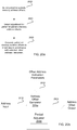
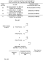
- An address offset generator may in response to a memory address offset instruction (also referred to as an offset address instruction) generates a periodic pattern of memory address offsets as a function of a period.
- an address offset generator may be configured to generate periodic address offsets for inverting data in a diagonal pattern of memory cells, for example, as a function of the number of rows or the number of columns of memory region under test.
- the defect detection and repair circuit 108 may be activated to test for and repair memory defects during the manufacture process at the wafer or die level but also after semiconductor components have been assembled and packaged. If the defect detection and repair circuit is located on a separate die such as a logic device, the defect detection and repair circuit may be used to test the memory device or devices after the memory has been connected to a device containing the defect detection and repair circuit. Further, it is appreciated that in some embodiments, the internal defect detection and repair circuit 108 may be activated to test for and repair memory defects should a memory failure occur after the device 100 has been packaged in a housing and sold to consumers. Thus, the internal defect detection and repair circuit 108 may interrupt normal memory transactions between the processor 102 and memory 104 to conduct memory test and repair operations.
- the computer architecture device 100 may further include storage 116 (e.g., a non-volatile storage, such as magnetic disk drives, optical disk drives, a tape drive, flash memory, etc.).
- the storage 116 may comprise an internal storage device or an attached or network accessible storage. Programs in the storage 116 are loaded into the memory 104 and executed by the processor 102 in a manner known in the art.
- the computer architecture device 100 further includes a network controller or adapter 118 to enable communication with a network, such as an Ethernet, a Fiber Channel Arbitrated Loop, etc.
- the architecture may, in certain embodiments, include a video controller 120 to render information on a display monitor, where the video controller 120 may be embodied on a video card or integrated on integrated circuit components mounted on a motherboard or other substrate.
- An input device 122 is used to provide user input to the processor 102, and may include a keyboard, mouse, pen-stylus, microphone, touch sensitive display screen, input pins, sockets, or any other activation or input mechanism known in the art.
- An output device 124 is capable of rendering information transmitted from the processor 102, or other component, such as a display monitor, printer, storage, output pins, sockets, etc.
- the network adapter 118 may embodied on a network card, such as a Peripheral Component Interconnect (PCI) card, PCI-express, or some other I/O card, or on integrated circuit components mounted on a motherboard or other substrate.
- PCI Peripheral Component Interconnect
- the internal defect detection and repair circuit 108 includes a portal 126 through which test and repair input and output information may be passed among the defect detection and repair circuit 108 and the other components of the device 100 and if appropriate, to devices external to the computer architecture device 100 via an input device 122 and an output device 118.
- a portal 126 is an on-chip communication network or fabric side band.
- the portal 126 may be accessed externally through a Test Access Port (TAP) system.
- TAP Test Access Port
- Other communication portals may be utilized, depending upon the particular application.
- a network router may lack a video controller 120, for example.
- any one or more of the components of the computer architecture device 100 may include one or more integrated circuits having an on-die defect detection and repair circuit as described herein.
- FIG. 2 shows a more detailed example of an internal defect detection and repair circuit 108 in accordance with the present description.
- the defect detection and repair circuit 108 includes a test pattern generator 210 for generating test patterns, writing test data to the memory device, sending a copy of the data to a defect detector circuit 220, and sending a series of read commands to read back the test data.
- the read data from the memory device is routed to the defect detector circuit 220 where the expected data from the test patter generator 210 is compared to the actual data from the memory device to detect defective memory cells in the memory 104 in response to the test patterns testing the memory cells of the memory 104.
- the defect detector circuit 220 stores in a memory 224 configured as a repair list repository also disposed within the device 108, a list of memory locations of the memory 104, each memory location of the list having a set of memory cells which includes at least one defective memory cell in the memory 104.
- the self-repair logic circuit 114 includes logic circuitry adapted to read the list of memory locations stored in the repair list repository 224, and to repair the memory locations of the list. In the illustrated embodiment, the memory locations of the list may be repaired by substituting a memory location of spare memory cells 230 of the memory 104, for a memory location having at least one defective memory cell.
- the repair list repository may also include register or other memory locations for various flags 234. For example, a flag may be set indicating that the number of memory locations having at least one defective memory cell exceeds the maximum for a particular memory region of the memory 104. Another flag may be set for each memory region, indicating whether at least one row of the particular memory region has at least one defective memory cell within the particular memory region. Other flags 234 may be stored in the repair list repository 224, depending upon the particular application.
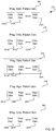
- FIGs. 3a , 3b , 3f , 4 show a more detailed example of the test pattern generator 210 of FIG. 2 , in accordance with one embodiment of the present description.
- the logic depicted in FIGs. 3a , 3b , 4 may be implemented in one embodiment, with a hardware finite state machine on board the die of the memory controller 106.
- This finite state machine may in turn be implemented with hardware logic gates or a software or firmware programmable processor or a combination thereof on the same die as the memory controller 104 or other internal die of the device 100.
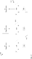
- the test pattern generator 210 includes a plurality of generators including a programmable address pattern generator 306 which includes at least one address generator 310a, 310b ... 310n ( FIG. 3f ), and a loop sequencer circuit 320 adapted to apply to an appropriate one or more of the generators 310a, 310b ... 310n of the programmable address generator 306, a plurality of nested loop instructions, including a sequential loop 322 ( FIG. 3b ) of address instructions in a sequence 324 ( FIG. 3a ) of address instructions, Address Instruction 1, Address Instruction 2 ... Address Instruction n, to an address generator 310a, 310b ... 310n.
- the test pattern generator 210 ( FIG. 2 ) is adapted to execute memory commands at memory cells addressed by a pattern of memory cell addresses generated by an address instruction, Address Instruction 1, Address Instruction 2 ... Address Instruction n, being executed in sequence in the loop 322 ( FIG.
- a counter of the counters 323 of the instruction loop sequencer 320 generates a pointer to the sequence 324 ( FIG. 3a ) of address instructions, Address Instruction 1, Address Instruction 2 ... Address Instruction n, which in turn generates the current address instruction to be used.
- Parameters of the address instructions may include parameters identifying the size of the memory region to be tested, a starting address of the memory region to be tested, and a parameter indicating that a particular address instruction is the last address instruction of the sequence. Additional examples of parameters for address instructions are provided below. It is appreciated that other parameters may be included or utilized, depending upon the particular application.
- FIG. 3b shows a plurality 328 of nested instruction loops including a data instruction loop 330 nested within the address instruction loop 322, an algorithm instruction loop 332 nested within the data instruction loop 330, a command instruction loop 334 nested within the algorithm instruction loop 332, and selectable offset instruction loops 336a, 336b of a set 337 of offset instructions nested within the command instruction loop 334. It is appreciated that in some embodiments, the number and type of nested instruction loops may differ from those illustrated and the order of nesting may be changed as well, depending upon the particular application.
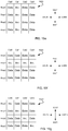
- FIG. 3c shows an example of an address pattern which may be generated by one of the address generators 310a, 310b ... 310n such as address generator 310a, for example, in response to one of the address instructions, Address Instruction 1, Address Instruction 2 ... Address Instruction n, such as Address Instruction 1, for example, for a memory region 338 of memory cells 340 of the memory 104.
- the memory region 338 is represented by a four by four array of memory cells 340 arranged in columns and rows.
- a typical memory region may be substantially larger and thus may have memory cells numbering in the kilobytes, megabytes, gigabytes, terabytes or more.
- One example of a memory region is often referred to as a "bank.”
- Each memory cell 340 may store a single bit, a byte, a word or a longer string of bits, depending upon the particular application.
- the address pattern generated is a "walking" pattern in which the generated address of the address pattern "walks" to the next adjacent memory cell of a particular column of memory cells 340.
- the address pattern may start at a particular memory cell address which may be represented as an ordered pair of a column address and a row address such the column-row address (0, 0) depicted in FIG. 3c .
- the next address of this particular address pattern may be generated by incrementing the row address portion of the memory cell address to the column-row address (0, 1) depicted in FIG. 3c .
- the remaining addresses of the remaining memory cells of the column are sequentially generated in this fashion.
- the row address portion may be reset to the original row address and the column address may be incremented to the column-row address (1, 0) depicted in FIG. 3c .
- the remaining addresses of the memory remaining memory cells of the region 338 are sequentially generated in this fashion.
- the final column-row address (3, 3) of the address pattern is depicted in FIG. 3c .
- the address pattern which is generated may be readily changed by changing the address instruction, or changing the address generator to which the address instruction is applied, or both.
- the direction of cell walking may be reversed from that shown in FIG. 3c , by providing an appropriate address instruction to an address generator.
- Other address patterns may walk up one column and then walk down another column, for example.
- Other address patterns may walk across a row before changing to a different row instead of walking up or down a column.
- Other address patterns for traversing a memory which are suitable for stress testing a memory may be readily implemented by appropriate selection of address instructions and address generator designs.
- parameters of the address instruction may include a parameter defining address generation direction. It is appreciated that other parameters may be included or utilized, depending upon the particular application. It is appreciated that providing multiple address instructions for multiple address generators facilitates implementation of a suitable stress tests for a memory.
- the sequence 324 ( FIG. 3a ) of address instructions, Address Instruction 1, Address Instruction 2 ... Address Instruction n, applied to the address generators 310a, 310b ... 310n, may comprise a sequence of four address instructions, for example. It is appreciated that the number of address instructions in a sequence of address instructions, may vary, depending upon the particular application.
- the test pattern generator 210 further includes a programmable data pattern generator 342 which includes at least one data generator 344a, 344b ... 344n ( FIG. 3f ).
- the loop sequencer circuit 320 is adapted to apply to appropriate ones of the data generators 344a, 344b ... 344n, a plurality of nested loop instructions, including a sequential loop 330 ( FIG. 3b ) of data instructions in a sequence 346 ( FIG. 3a ) of data instructions, Data Instruction 1, Data Instruction 2 ... Data Instruction n.
- a counter of the counters 323 of the instruction loop sequencer 320 generates a pointer to the sequence 346 ( FIG. 3a ) of data instructions, which in turn generates the current address instruction to be used.
- a parameter of the data instructions may include a parameter indicating that a particular data instruction is the last address instruction of the sequence. It is appreciated that other parameters may be included or utilized, depending upon the particular application.
- Each data generator 344a, 344b ... 344n may include one or more finite state machines. Each data instruction, Data Instruction 1, Data Instruction 2 ... Data Instruction n, of the sequence 346 when executed by an appropriate one of the data generators 344a, 344b ... 344n, causes that data generator 344a, 344b ... 344n to generate a data pattern as a function of the particular data instruction, Data Instruction 1, Data Instruction 2 ... Data Instruction n, and the particular data generator 344a, 344b ... 344n, to which it is applied.
- the test pattern generator 210 ( FIG. 2 ) is adapted to execute memory commands at memory cells to write a pattern of test data generated by a data instruction being executed in sequence 346 in the loop 330 ( FIG. 3b ) of data instructions, Data Instruction 1, Data Instruction 2 ... Data Instruction n, in memory cells addressed by a pattern of memory cell addresses generated by an address instruction being executed in sequence in the loop of address instructions.
- a data generator such as the data generator 344a, for example, of the programmable data pattern generator 342, may generate a string of data bits, such as all ones, for example, in response to one of the data instructions such as Data Instruction 1, for example.
- a generated data bit of the generated data pattern is written, for example, into each memory cell 340 by the test pattern generator 210 as the address generator 310a, for example, in response to one of the address instructions, such as Address Instruction 1, for example, generates the walking address pattern depicted for a memory region 338 of memory cells 340 of the memory 104.
- Other examples of data patterns which may be generated by the programmable data pattern generator 342 include strings of 0's, checkerboard patterns of alternating 1's and 0's, etc. depending upon the particular application.
- the data output by the programmable data pattern generator 342 may be used as write data, for example, to stress test the memory 104 as commands are executed at memory addresses traversing the memory 104.
- parameters of the data instruction may include parameters indicating whether to invert data and indicating various data backgrounds such as solid, column stripes, row stripes, checkerboard etc. It is appreciated that other parameters may be included or utilized, depending upon the particular application.
- the sequence 346 ( FIG. 3a ) of data instructions, Data Instruction 1, Data Instruction 2 ... Data Instruction n, applied to the appropriate data generators 344a, 344b ... 344n, may comprise a sequence of four data instructions, for example. It is appreciated that the number of data instructions in a sequence of data instructions, may vary, depending upon the particular application.
- the test pattern generator 210 further includes a programmable algorithm pattern generator 350 which includes at least one algorithm generator 354a, 354b ... 354n ( FIG. 3f ).
- the loop sequencer circuit 320 is adapted to apply to appropriate ones of the algorithm generators 354a, 354b ... 354n, a plurality of nested loop instructions, including a sequential loop 332 ( FIG. 3b ) of algorithm instructions in a sequence 356 ( FIG. 3a ) of algorithm instructions, Algorithm Instruction 1, Algorithm Instruction 2 ... Algorithm Instruction n.
- a counter of the counters 323 of the instruction loop sequencer 320 generates a pointer to the sequence 356 ( FIG.
- Each algorithm generator 354a, 354b ... 354n may include one or more finite state machines.
- Each algorithm instruction, Algorithm Instruction 1, Algorithm Instruction 2 ... Algorithm Instruction n, of the sequence 356 when executed by an appropriate one of the algorithm generators 354a, 354b ... 354n, causes that algorithm generator 354a, 354b ... 354n to generate a test data pattern as an output of an algorithm.
- the programmable algorithm test generator 350 inputs the data pattern generated by the programmable data pattern generator 342, and modifies the input data pattern to a modified data pattern in accordance with the algorithm of the selected algorithm generator 354a, 354b ... 354n executing the selected algorithm instruction, Algorithm Instruction 1, Algorithm Instruction 2 ... Algorithm Instruction n, of the sequence 356. In other embodiments, the programmable algorithm test generator 350 generates a data pattern as a function of the particular algorithm instruction, Algorithm Instruction 1, Algorithm Instruction 2 ... Algorithm Instruction n, and the particular algorithm generator 354a, 354b ... 354n, to which it is applied, without inputting the data pattern generated by the programmable data pattern generator 342.
- the test pattern generator 210 ( FIG. 2 ) is adapted to execute memory commands at memory cells to write a data test pattern in accordance with an algorithm instruction being executed in sequence 356 in the loop 332 of algorithm instructions, Algorithm Instruction 1, Algorithm Instruction 2 ... Algorithm Instruction n, in memory cells addressed by a pattern of memory cell addresses generated by an address instruction being executed in sequence in the loop of address instructions.
- the data output by the programmable algorithm test generator 350 may be used as write data, for example, to stress test the memory 104 as commands are executed at memory addresses traversing the memory 104.
- the data output by the programmable algorithm test generator 350 may also be used as expected test result data to compare to actual test data obtained as the memory 104 is stress tested.
- the generated data patterns may also be used as control signals to control the control signal inputs of the memory 104.
- One example of an algorithm which may be generated by a selected algorithm generator 354a, 354b ... 354n, such as the algorithm generator 354a, for example, executing a selected algorithm instruction, Algorithm Instruction 1, Algorithm Instruction 2 ... Algorithm Instruction n, such as the Algorithm Instruction 1, for example, of the sequence 356, is a shift register based random pattern algorithm which may be used for testing interconnects of the memory 104, for example.
- These random patterns generated by an algorithm generator such as the algorithm generator 354a, for example, executing a selected algorithm instruction, such as the Algorithm Instruction 1, for example, are believed to create white noise on an interconnect to stress the interconnect to test for a defect.
- the random pattern may be generated by modifying a test data pattern generated by a generator of the programmable data pattern generator 342, using an algorithm generator of the programmable algorithm pattern generator 350.
- the random pattern may be generated by an algorithm generator of the programmable algorithm pattern generator 350 without modifying a test data pattern generated by a generator of the programmable data pattern generator 342.
- Another example an algorithm which may be generated by a selected algorithm generator 354a, 354b ... 354n, such as the algorithm generator 354b, for example, executing a selected algorithm instruction, Algorithm Instruction 1, Algorithm Instruction 2 ... Algorithm Instruction n, such as the Algorithm Instruction 2, for example, of the sequence 356, is a neighbor interaction based address walking algorithm.
- This algorithm may be used, for example, for testing memory cells of dynamic random access memories which are primarily capacitive in nature. In accordance with the neighbor interaction based address walking algorithm, if all neighboring cells in the memory are switched, a cross coupling effect may cause a cell under test to flip to the wrong digital value.
- FIG. 3d shows an example of a neighbor interaction based address walking algorithm which may be generated by the algorithm generator 354b, for example, executing the Algorithm Instruction 2, for example, of the sequence 356, for a memory region 358 of memory cells 340 of the memory 104.
- the memory region 358 is represented by a seven by twelve array of memory cells 340 arranged in columns and rows.
- the test pattern generator 210 FIG. 2 is adapted to execute a first set of memory commands, write (Wr 1) and read (Rd 1) at a first neighbor memory cell 340b, a second set of memory commands, write (Wr 2) and read (Rd 2) at a second neighbor memory cell 340b, and so on finishing with an eighth set of memory commands, write (Wr 8) and read (Rd 8) at an eighth neighbor memory cell 340d, in accordance with a neighbor interaction based address walking algorithm which may be generated by the algorithm generator 354b, for example, executing the Algorithm Instruction 2, for example, of the sequence 356.
- Parameters of the algorithm instructions may further include parameters indicating the starting command of a sequence of commands, the starting address direction for that sequence of commands, whether data is to be inverted, one or more wait periods to prevent a new algorithm instruction from beginning until the wait condition is satisfied, whether to reset a counter such an instruction counter for a sequence of instructions such as a sequence of command instructions, for example. It is appreciated that other parameters may be included or utilized, depending upon the particular application.
- the algorithm instructions, Algorithm Instruction 1, Algorithm Instruction 2 ... Algorithm Instruction n, of the sequence 356 when executed by an appropriate one of the algorithm generators 354a, 354b ... 354n may implement other algorithms for stress testing the memory 104, depending upon the particular application.
- the sequence 356 ( FIG. 3a ) of algorithm instructions, Algorithm Instruction 1, Algorithm Instruction 2 ... Algorithm Instruction n applied to the appropriate algorithm generators 354a, 354b ... 354n may comprise a sequence of eight algorithm instructions, for example. It is appreciated that the number of algorithm instructions in a sequence of algorithm instructions, may vary, depending upon the particular application.
- the test pattern generator 210 further includes a programmable command pattern generator 360 which includes at least one command generator 364a, 364b ... 364n ( FIG. 3f ).
- the loop sequencer circuit 320 is adapted to apply to appropriate ones of the command generators 364a, 364b ... 364n, a plurality of nested loop instructions, including a sequential loop 334 ( FIG. 3b ) of command instructions in a sequence 366 ( FIG. 3a ) of command instructions, Command Instruction 1, Command Instruction 2 ... Command Instruction n.
- a counter of the counters 323 of the instruction loop sequencer 320 generates a pointer to the sequence 366 ( FIG. 3a ) of command instructions, which in turn generates the current command instruction to be used.
- a parameter of the command instructions may include a parameter indicating that a particular command instruction is the last command instruction of the sequence. It is appreciated that other parameters may be included or utilized, depending upon the particular application.
- Each command generator 364a, 364b ... 364n may include one or more finite state machines.
- Each Command instruction, Command Instruction 1, Command Instruction 2 ... Command Instruction n, of the sequence 366 when executed by an appropriate one of the command generators 364a, 364b ... 364n, causes that command generator 364a, 364b ... 364n to generate a pattern of commands as a function of the particular selected command generator and the particular selected command instruction.
- the test pattern generator 210 ( FIG. 2 ) is adapted to execute a pattern of memory commands at memory cells in accordance with a command instruction being executed in sequence 366 in the loop 334 of command instructions, Command Instruction 1, Command Instruction 2 ... Command Instruction n, in memory cells addressed by a pattern of memory cell addresses generated by an address instruction being executed in sequence in the loop of address instructions.
- the data of the write commands is provided by one or both of the programmable data pattern generator 342 and the programmable algorithm generator 350 as discussed above.
- the generated data patterns may also be used for control signal commands of the programmable command pattern generator 360 to control the control signal inputs of the memory 104.
- the sequence 366 ( FIG. 3a ) of command instructions, Command Instruction 1, Command Instruction 2 ... Command Instruction n, which are applied to the appropriate command generators 364a, 364b ... 364n, may comprise a sequence of twenty-four command instructions, for example. It is appreciated that the number of command instructions in a sequence of command instructions, may vary, depending upon the particular application.
- each command instructions, Command Instruction 1, Command Instruction 2 ... Command Instruction n may instruct an appropriate command generator of the command generators 364a, 364b ... 364n to generate a single command such as a memory write or memory read command, for example.
- each command instruction, Command Instruction 1, Command Instruction 2 ... Command Instruction n may instruct an appropriate command generator of the command generators 364a, 364b ... 364n to generate a sequence of commands.
- FIG. 3e depicts a multi-part stress test which employs a sequence of commands. In part 1 of the stress test of FIG. 3e , in a manner similar to that of the stress test pattern depicted in FIG.
- a single command in this example, a write command
- the programmable address pattern generator 306 generates a pattern of addresses which walks through the memory region 338 as shown, to initialize the memory region 338.
- a sequence of commands in this example, a quick read command (R) followed by a write inverse (Wbar) command, is executed for each memory cell of the same memory region 338, as the programmable address pattern generator 306 again generates the same pattern of addresses generated in part 1, which again walks through the memory region 338 a second time as shown.
- a quick read inverse (Rbar) command followed by a write (W) command is executed for each memory cell of the same memory region 338, as the programmable address pattern generator 306 again generates the same pattern of addresses generated in parts 1 and 2, which again walks through the memory region 338 a third time as shown.
- each command instruction may be applied to a common finite state machine of a command generator. It is appreciated that in other embodiments, command instructions may be applied to different finite state machine of various command pattern generators.
- each command instruction defines one command to execute .
- a sequence of commands may be provided by a sequence of command instructions, each of which may be applied to a particular memory address in sequence. The sequence of commands may then be applied over a sequence of different addresses, one address location at a time over the course of a stress test. It is appreciated that in other embodiments, a command instruction may define more than one command in a sequence.
- parameters of a command instruction may include parameters indicating a read or write command, whether data for the command is to be inverted, identifying an alternate data source, and a "hammer" function" in which specifies repeated write operations. It is appreciated that other parameters may be utilized, depending upon the particular application.
- the test pattern generator 210 further includes a programmable address offset pattern generator 370 which includes at least one offset generator of the offset generators 374a, 374b ... 374n ( FIG. 3f ). Each offset generator 374a, 374b ... 374n is adapted to generate a pattern of address offsets to offset a base address generated by the programmable address pattern generator 306.
- the loop sequencer circuit 320 is adapted to apply to appropriate ones of the offset generators 374a, 374b ... 374n, a plurality of nested loop instructions, including a selected sequential loop 336a, 336b ( FIG. 3b ) of offset instructions in a sequence 376 ( FIG. 3a ) of offset instructions, Offset Instruction 1, Offset Instruction 2 ...
- Offset Instruction n A counter of the counters 323 of the instruction loop sequencer 320, generates a pointer to the sequence 376 ( FIG. 3a ) of offset instructions, which in turn generates the current offset instruction to be used.
- a parameter of the offset instructions may include a parameter indicating that a particular offset instruction is the last offset instruction of the sequence. It is appreciated that other parameters may be included or utilized, depending upon the particular application.
- Each offset generator 374a, 374b ... 374n may include one or more finite state machines.
- Each Offset instruction, Offset Instruction 1, Offset Instruction 2 ... Offset Instruction n, of the sequence 376 when executed by an appropriate one of the offset generators 374a, 374b ... 374n, causes that offset generator 374a, 374b ... 374n to generate a pattern of address offsets as a function of the particular selected offset generator and the particular selected offset instruction.
- the test pattern generator 210 in executing memory commands at memory cells is adapted to execute a pattern of commands generated by a command instruction being executed in sequence 366 in the loop 334 of command instructions in memory cells addressed by a pattern of memory cell addresses generated by an address instruction being executed in sequence 324 in the loop 322 of address instructions and offset by the pattern of memory address offsets generated by a memory address offset instructions, Offset Instruction 1, Offset Instruction 2 ... Offset Instruction n, being executed in sequence 376 in the loop 336a, 336b of memory address offset instructions.
- a base address of the address pattern generated by the programmable address pattern generator 306 may be offset by one or more address offsets of the offset pattern generated by the programmable offset pattern generator 370.
- the data of the write commands is provided by one or both of the programmable data pattern generator 342 and the programmable algorithm generator 350 as discussed above.
- the sequence 376 ( FIG. 3a ) of offset instructions, Offset Instruction 1, Offset Instruction 2 ... Offset Instruction n, which are applied to the appropriate offset generators 374a, 374b ... 374n, may comprise a sequence of two offset instructions, for example. It is appreciated that the number of offset instructions in a sequence of offset instructions, may vary, depending upon the particular application.
- one loop of offset instructions such as loop 336a, for example, may be a loop of offset address instructions which create a variety of possible offset operations in an address range relative to the current base address.
- the offset address commands allow a sequence of offset address commands, such as a sequence of six offset address commands, for example, to be sequentially executed in each loop 336a.
- An offset address instruction of this loop may include parameters indicating the direction of offset such as north, south, east or west of the base address, for example, whether a stripe is involved, and that a particular offset address instruction is the last offset address instruction of the sequence.
- the stripe function disables the normal carry from row to column or column to row during the offset address increments. It is appreciated that other parameters may be included or utilized, depending upon the particular application.
- one loop of offset instructions such as loop 336b, for example, may be a loop of offset command instructions that may be sequentially executed in the loop 336b.
- An offset address instruction of this loop may include parameters indicating a read or write command, whether data for the offset command is to be inverted, identifying an alternate data source, whether to use the base address or an offset address, a "hammer" function" which specifies repeated write operations, and that a particular offset command instruction is the last offset command instruction of the sequence. It is appreciated that other parameters may be utilized, depending upon the particular application.
- an offset instruction as described above may be substituted for a current command instruction by setting an offset command substitution parameter of the command instruction of the sequence 366.
- the offset loop 336a, 336b of the offset command to be substituted may be indicated by an offset loop identifying parameter of the command instruction of the sequence 366.
- FIG. 3d shows an example of a neighbor interaction based address walking algorithm stress test. In this stress test, a memory cell 340a designated "Base" is stressed by neighbors cells within two cells away from it. The base address which is the address of the memory cell 340a, is generated by the programmable address generator 306.
- the addresses of the neighbors of the base cell 340a are generated by modifying the base address of the base cell 340a with the address offsets generated by the programmable address offset pattern generator 370.
- the address of the neighbor cell 340b may be generated by adding a column offset of "one" to the address of the base cell 340.
- the address of the neighbor cell 340c may be generated by adding a column offset of "two" to the address of the base cell 340a or may be generated by adding a column offset of "one” to the generated address of the neighbor cell 340b.
- the address of the neighbor cell 340d may be generated by subtracting a row offset of "two" from the address of the base cell 340a.
- the address offsets may be generated by the offset generator 374a, for example, executing the Offset Instruction 1, for example.
- test pattern generator 210 ( FIG. 2 ) is adapted to execute a first set of memory commands, write (Wr 1) and read (Rd 1) at a first neighbor memory cell 340b, a second set of memory commands, write (Wr 2) and read (Rd 2) at a second neighbor memory cell 340b, and so on finishing with an eighth set of memory commands, write (Wr 8) and read (Rd 8) at an eighth neighbor memory cell 340d, in accordance with a neighbor interaction based address walking algorithm at addresses which may be generated by the programmable address generator 306, offset by the address offset pattern generated by the programmable address offset generator 370.
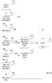
- FIG. 4 depicts one example of operations of the self-test logic 110 of FIG. 1 implementing the nested loop structure depicted in FIG. 3b .
- the instruction sequences may In a first operation, address instruction selection is initialized (block 410) to select the first address instruction such as Address Instruction 1, for example. It is appreciated that address instruction selection may be initialized to select another address instruction of the sequence 324 of address instructions, depending upon the particular application.
- data instruction selection is initialized (block 412) to select the first data instruction such as Data Instruction 1, for example, algorithm instruction selection is initialized (block 414) to select the first algorithm instruction such as Algorithm Instruction 1, for example, command instruction selection is initialized (block 416) to select the first command instruction such as Command Instruction 1, for example, and if there is an offset (block 417) an offset instruction selection is initialized (block 418) to select the first offset instruction such as Offset Instruction 1, for example.
- data, algorithm, command and offset instruction selection may be initialized to select another instruction of the respective sequences 346, 356, 366, and 376, of instructions, depending upon the particular application.
- the instructions may be applied to the appropriate generators of the programmable pattern generators 306, 342, 350, 360 and 370 and executed (block 420) to generate the selected address, data, algorithm, command and offset patterns to generate the appropriate stress tests of the memory 104.
- FIG. 3c discussed above depicts a stress test which employs a single command, a write command in this example, which is generated by the programmable command pattern generator 360 in response to the Command Instruction 1, in this example.
- the write command is executed for each memory cell of the memory region 338, as the programmable address pattern generator 306 in response to the Address Instruction 1, in this example, generates a pattern of addresses which walks through the memory region 338 as shown, to initialize the memory region 338.
- the same bit (or bits if a multi-bit cell) may be written into each memory cell of the memory region 338, or the bits may vary from cell to cell, as defined by the data pattern generated by the programmable data pattern generator 342 in response to the Data Instruction 1, in this example.
- the stress test of FIG. 3c does not employ address offsets and accordingly, the programmable offset pattern generator 370 may, in response to the Offset Instruction 1, pass the addresses generated by the programmable address pattern generator 306 unmodified.
- the walking pattern may be generated by sequentially applying column and row offsets to a base address generated by the programmable address pattern generator 306.
- the programmable algorithm pattern generator 350 in response to the Algorithm Instruction 1, may pass the write data generated by the programmable pattern generator 342 unmodified by a particular algorithm.
- the memory defect detector 220 compares (block 422, FIG. 4 ) the results of the stress test to expected values and identifies defects (if any) in the memory region or regions tested and stores appropriate defect location data in the repair list repository 224 ( FIG. 2 ) of failing addresses.
- the self-test logic 110 executes a nested loop 336a, 336b ( FIG. 3b ) of offset instructions, nested within the command instruction loop 334.
- a determination is made as to whether all of the offset instructions of the offset instruction sequence 376 ( FIG. 3a ) have been selected. If not, the next offset instruction, such as Offset Instruction 2, for example, in the sequence 376 of offset instructions is selected (block 426) for the programmable offset pattern generator 370. Since the offset instruction loop 336a, 336b is nested within the command loop 334, the command instruction as well as the algorithm , data and address instructions remain unchanged at this point.
- the selected offset instruction together with the initial instructions selected for the programmable pattern generators 306, 342, 350, and 360 may be applied to the appropriate generators of the programmable pattern generators 306, 342, 350, 360 and 370 and executed (block 420) to generate the selected address, data, algorithm, command and offset patterns to generate the appropriate stress tests of the memory 104.
- the selected command instruction together with the initial instructions selected for the programmable pattern generators 306, 342, 350 and 370 may be applied to the appropriate generators of the programmable pattern generators 306, 342, 350, 360 and 370 and executed (block 420) to generate the selected address, data, algorithm, command and offset patterns to generate the appropriate stress tests of the memory 104.
- FIG. 3e depicts a multi-part stress test which employs a sequence of commands, which may be generated by the programmable command generator 360.
- a single command in this example, a write command
- an initial command instruction such as Command Instruction 1
- the programmable address pattern generator 306 generates in response to an initial address instruction, such as Address Instruction 1, for example, a pattern of addresses which walks through the memory region 338 as shown, to initialize the memory region 338.
- a sequence of commands in this example, a quick read command (R) followed by a write inverse (Wbar) command, is executed for each memory cell of the same memory region 338, as the programmable address pattern generator 306 again generates the same pattern of addresses generated in part 1, which again walks through the memory region 338 a second time as shown for part 2.
- R quick read command
- Wbar write inverse
- the second sequence of commands (a quick read command (R) followed by a write inverse (Wbar) command) of part 2 may be generated in response to a second selected command instruction such as Command Instruction 2, for example, as the programmable address pattern generator 306 generates in response to the unchanged initial address instruction, such as Address Instruction 1, for example, the same pattern of addresses which again walks through the memory region 338 for part 2 of the stress test.
- each command may be generated in response to a single command instruction.
- a quick read inverse (Rbar) command followed by a write (W) command is executed for each memory cell of the same memory region 338, as the programmable address pattern generator 306 again generates the same pattern of addresses generated in parts 1 and 2, which again walks through the memory region 338 a third time as shown for part 3.
- the sequence of commands of part 3 may be generated in response to a third selected command instruction.
- the sequence of commands of part 3 may be generated in response to a single command instruction which also generated the commands of parts 1 and 2 of the stress test.
- FIG. 3d shows an example of a neighbor interaction based address walking algorithm stress test as discussed above.
- one or more offset instructions may be employed in the sequence 376 of offset instructions to generate appropriate offset addresses to address the neighbor cells of the base cell as shown.
- one or more command instructions may be employed in the sequence 366 of command instructions to generate the appropriate sequence of commands for each neighbor cell as shown.
- a determination (block 434) is made as to whether all of the algorithm instructions of the algorithm instruction sequence 356 ( FIG. 3a ) have been selected. If not, the next algorithm instruction, such as Algorithm Instruction 2, for example, in the sequence 356 of algorithm instructions is selected (block 436) for the programmable algorithm pattern generator 350. Since the algorithm instruction loop 332 is nested within the data instruction loop 330, the data instruction as well as the address instruction remain unchanged at this point.
- command instruction selection is reinitialized (block 416) as well as the offset instruction selection (block 418) to the first instruction of the respective instruction sequence 366, 376 ( FIG. 3a ).
- next selected algorithm instruction together with the initial instructions selected for the programmable pattern generators 306, 342, 350, 360 and 370 may be applied to the appropriate generators of the programmable pattern generators 306, 342, 350, 360 and 370 and executed (block 420) to generate the selected address, data, algorithm, command and offset patterns to generate the appropriate stress tests of the memory 104.
- a determination (block 438) is made as to whether all of the data instructions of the data instruction sequence 346 ( FIG. 3a ) have been selected. If not, the next data instruction, such as Data Instruction 2, for example, in the sequence 346 of data instructions is selected (block 440) for the programmable data pattern generator 342. Since the data instruction loop 330 is nested within the address instruction loop 322, the address instruction remains unchanged at this point. However, the algorithm instruction selection is reinitialized(block 414) as well as the command selection (block 416) and the offset instruction selection (block 418) to the first instruction of the respective instruction sequences 356, 366, 376 ( FIG.
- the selected data instruction together with the initial instructions selected for the programmable pattern generators 306, 350, 360 and 370 may be applied to the appropriate generators of the programmable pattern generators 306, 342, 350, 360 and 370 and executed (block 420) to generate the selected address, data, algorithm, command and offset patterns to generate the appropriate stress tests of the memory 104.
- a determination (block 442) is made as to whether all of the address instructions of the address instruction sequence 324 ( FIG. 3a ) have been selected. If not, the next address instruction, such as Address Instruction 2, for example, in the sequence 324 of address instructions is selected (block 444) for the programmable address pattern generator 306.
- the data instruction selection is reinitialized(block 412) as well as the algorithm instruction selection (block 414), command instruction selection (block 416) and the offset instruction selection (block 418) to the first instruction of the respective instruction sequences 346, 356, 366, 376 ( FIG. 3a ).
- the selected address instruction together with the initial instructions selected for the programmable pattern generators 342, 350, 360 and 370 may be applied to the appropriate generators of the programmable pattern generators 306, 342, 350, 360 and 370 and executed (block 420) to generate the selected address, data, algorithm, command and offset patterns to generate the appropriate stress tests of the memory 104.
- the test pattern generation is done (block 450) unless new instructions are loaded into the sequences 324, 346, 356, 366, 376, and executed, repeating the test pattern generation and execution depicted in FIG. 4 .
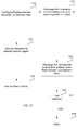
- FIG. 5 depicts one example of defect detection and recording operations of the defect detector circuit 220 of FIG. 2 .
- the logic depicted in FIG. 5 may be implemented in one embodiment, with a hardware finite state machine on board the die of the memory controller 106.
- This finite state machine may in turn be implemented with hardware logic gates or a software or firmware programmable processor or a combination thereof on the same die as the memory controller 104 or other internal die of the device 100.
- the defect detector circuit 220 detects (block 510) a failure of a memory cell in response to a stress test applied by the test pattern generator 210 using a stress test pattern generated by the test pattern generator 210.
- a stress test may include memory commands including read commands, write commands or both, or control signals or both, which are applied to the memory 104 or a region thereof. Data is read from the memory 104 and compared to expected results.
- the memory cells may be arranged in a plurality of memory regions and a fixed number of spare rows of memory cells may be available to be substituted for each row of memory cells containing a defective cell.
- a bank of memory cells for example, there may be a maximum of two spare rows of cells to available to replace rows having defective cells in that particular bank of cells. It is appreciated that the number of spare rows of cells available for a particular region may vary, depending upon the particular application.
- stress testing and repair is described herein with respect to rows and banks of memory cells, it is appreciated that stress testing and repair may be organized at other levels such as on a rank basis, or chip basis or any memory region or portion thereof.
- the number of spare rows may exceed the number of repair list repository locations for storing row addresses of rows containing defects, for a particular bank of memory. Accordingly, the maximum number of defects will be equal to the number of spare rows available or the number of repair list repository locations available, whichever is less, for a particular bank of the memory 104.
- repair list repository 224 it may not be cost effective in some embodiments to implement a repair list repository 224 with a relatively large number of locations for storing the addresses or rows needing repair. However if the number of repairable elements exceeds the number of repair list repository locations, the test and repair process may be repeated, finding additional failing rows on each iteration, referred to herein as two pass, three pass or n-pass testing. In this manner it may be possible to test and repair memory devices with a large number of defects, while employing a relatively limited number of repository locations.
- the number of spare rows (or repair list repository locations) available for each bank of the memory 104 may be set by a user setting a configuration register 232 ( FIG. 2 ), for example, via the portal 126 prior to the initiation of testing. In other embodiments, the number of spare rows (or repair list repository locations) available for each bank of the memory 104 may be set as a fixed value at the time of manufacture of the device 100.
- a determination may be made as to whether the number of memory locations such as rows, for example, having at least one defective memory cell exceeds a maximum for a particular memory region, such as a bank of memory cells, for example.
- a determination may be made by checking a flag (such as a flag of the flags 234 of FIG. 2 , for example) which when set, indicates that the failure maximum has been reached.
- a flag such as a flag of the flags 234 of FIG. 2 , for example
- the failure maximum flag provides an overflow indicator which indicates whether additional repair is possible for a particular bank.
- stress testing of a bank may continue after the failure maximum flag has been set to determine whether additional defects exist in that bank notwithstanding that additional spare rows (or additional repair list repository locations) are not available for use in connection replacement of any such additional defects.
- a failure maximum flag may be reset by a write operation to a configuration register of the flags 234 via the portal 126 or by an explicit reset operation.
- the row of the defective memory cell is new, that is, whether the defective memory cell is the first known defective memory cell of a set of memory locations such as a row of memory cells, for example.
- the memory may be repaired by replacing a row of memory cells containing a defective cell with an entire row of spare cells.
- the defect is not the first defect discovered for that row, and the detection and recording process is ended (block 514) for that particular defect.
- a row or other set of memory locations containing a defective memory cell may be designated for replacement in a memory configured as a repair list repository, such as the repair list repository 224 ( FIG. 2 ) of failing memory addresses.
- a repair list repository such as the repair list repository 224 ( FIG. 2 ) of failing memory addresses.
- it may be determined as to whether (block 518) the defective memory cell is the first known defective memory cell of a row of memory cells, for example, by determining if the row of memory cells containing the defective memory cell of a particular memory region of memory cells, has already been stored as an entry in the list of the repair list repository 224.
- the defective memory cell is determined to not be the first known defective cell of that row, and storing a designation of that row containing the defective memory cell in the repair list repository as an entry of the list of memory locations may be bypassed (block 514), since the particular row of memory cells of the particular memory region of memory cells has already been stored as an entry in the list of the repair list repository.
- the defective memory cell is the first known defective memory cell of a set of memory locations such as a row of memory cells, for example, a determination may be made as to whether the number of memory locations such as rows, for example, having at least one defective memory cell has reached (block 520) the maximum for a particular memory region, such as a bank of memory cells, for example. If so, the aforementioned failure maximum flag may be set (block 524) and the detection and recording process is ended (block 514) for that particular defect. In one embodiment, the failure maximum may be set to indicate when the supply of spare rows available for replacement of defective rows has been exhausted for a particular memory region.
- the row address of the row containing the defective memory cell may be stored (block 534) in an appropriate location of the repair list repository 224 ( FIG. 2 ) of failing addresses and a flag set (block 540) indicating that the address of a row of memory cells has been stored in the repair list repository 534 for repair of that row.
- This flag may be checked in a subsequent determination (block 530) as to whether there have been prior failures detected for that memory region.
- a flag may be set for each memory region, indicating whether at least one row of the particular memory region has at least one defective memory cell.
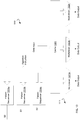
- FIG. 6 shows one example of repair list repository 224 of failing memory addresses.
- the structure of the repair list repository 224 has been arranged as an array of rows and columns of repository locations, in which each bank, Bank 0, Bank 1 ... Bank n, of the memory 104 has an assigned row of repository locations.
- the array of the repair list repository 224 has a column of locations, Fail 0, Fail 1, ... Fail n, for each spare memory row available to be assigned to replace a row of a particular bank of memory cells.
- the repair list repository 224 would have eight rows of repository locations, one row of repository locations for each bank, and four columns of repository locations, one column of repository locations for each available spare row of memory cells for that particular bank.
- the row address of the memory cell row of Bank 0 containing the defective memory cell may be placed in the repair list repository location, Bank 0, Fail 0, and a flag may be set (block 540) in the Bank 0 Flags location of the repair list repository 224, indicating that the address of a row of memory cells has been stored in the repair list repository 534 for repair of that memory cell row in Bank 0.
- a flag may be set (block 540) in the Bank 0 Flags location of the repair list repository 224, indicating that the address of a row of memory cells has been stored in the repair list repository 534 for repair of that memory cell row in Bank 0.
- the failure count is incremented (block 532) to point to repository location Bank 0, Fail 1, the next location in the row of repository locations for Bank 0, and the memory cell row address of that next new, unique row of Bank 0 containing the defective memory cell may be placed in the repair list repository location at Bank 0, Fail 1.
- a flag may be set (block 540) in the Bank 0 Flags location of the repair list repository 224, indicating that another address of a row of memory cells has been stored in the repair list repository 534 for repair of that memory cell row in Bank 0.
- the failure count is incremented (block 532) to point to the next repository location in the row of locations for Bank 0, and the memory cell row address of that next unique memory cell row of Bank 0 containing the defective memory cell may be placed in the repair list repository location corresponding to that failure count.
- a flag may be set (block 540) in the Bank 0 Flags location of the repair list repository 224, indicating that another address of a memory cell row of memory cells has been stored in the repair list repository 534 for repair of that row in Bank 0.
- Stress testing of Bank 0 continues until all of that bank has been stress tested with each of the programmed stress tests. As the stress testing of Bank 0 progresses, once the number of detected new, unique rows containing a defect exceeds the number of spare rows for Bank 0, the failure maximum is reached (block 520), and the failure maximum flag may be set (block 524) in the Bank 0 Flags location in the repair list repository 224. At that point, no additional memory cell row addresses are recorded (block 514) in the repair list repository since no additional spare rows remain for Bank 0. However, stress testing of Bank 0 may continue, in one embodiment, even after the failure maximum is reached, to identify whether additional defects exist in Bank 0. In other embodiments, stress testing of a particular bank may be terminated once the failure maximum has been reached.
- the failure count as indicated by the failure counter may be reset either automatically or by a user or external software resetting the failure counter prior to the initiation of testing of the next bank of the memory 104.
- the failure counter may be maintained as a register in the flags 234 and accessed via the portal 126 to be read or reset as appropriate. Also, in some embodiments, a separate failure counter may be maintained for each bank or other memory region of the memory 104 .
- Stress testing of the memory 104 continues, stress testing the remaining banks, Bank 1, Bank 2 ... Bank n, wherein the memory cell row addresses of new, unique memory cell rows containing defects are recorded in the repair list repository 224 in a manner similar to that described above for Bank 0.
- flags may be set for each bank as stress testing progresses for each bank, as described above.
- the self-repair logic 114 may automatically commence repairing the defective memory 104 by replacing the row of cells containing a defect, with a spare row of memory cells, without user or external software intervention.
- the self-repair logic 114 may operate in parallel with the self-test logic 100 such that the memory 104 may be repaired in parallel with ongoing stress testing of the memory to identify additional rows if any containing a defective memory cell.
- the repair logic may be activated once all stress tests are complete and all defective memory cells rows have been recorded in the repository 224.
- the repair logic may be activated once all stress tests are complete for a particular memory region such as a bank, for example, and all defective memory cells rows have been recorded in the repository 224 for that bank. As such, stress tests may be resumed to identify any memory defects in one bank while defective memory cell rows already recorded in the repair list repository 224 are repaired for another bank.
- the repair logic may be activated to repair memory cell rows as soon as defective memory cell rows are recorded in the repair list repository without waiting for stress testing to be completed for a particular memory region such as a bank, for example.
- the contents of the repair repository including the addresses of rows with at least one defective cell and the associated flags may be read out by hardware or software and saved for later use in repair.
- the repair may be conducted as failures are detected, or after all stress tests have completed.
- the repair may be deferred to a later time in the same test step or even to some other future test step.
- the repair data is stored in volatile registers it may be required to copy the data to some other permanent storage, either on-die or off-die, such as over a network or storage device before removing power from the repository 224. Storing the repair data in this way may not only facilitate deferred repair but may also serve as a permanent record of failure rates such as might be employed in process tracking for quality management or other purposes.
- FIG. 7 illustrates a more detailed example of the self-repair logic 114 of FIG. 1 , in accordance with one embodiment of the present description.
- the logic depicted in FIG. 7 is a repair engine implemented in one embodiment, with a hardware finite state machine on board the die of the memory controller 106.
- This finite state machine may in turn be implemented with hardware logic gates or a software or firmware programmable processor or a combination thereof on the same die as the memory controller 104 or other internal die of the device 100.
- the repair logic 114 cycles through the list of failing addresses collected by the self-test logic 110 and recorded in the repair list repository 224. For each failing memory cell row, the row address of which is recorded in a repository location of the repository 224, the repair logic 114 issues appropriate commands to the memory 104 to replace the failing or failed row with a spare row built into the memory 104.
- a first state 710 the state machine of the repair logic 114 is idle, awaiting recordation of a row address of a defective memory cell row in the repair list repository 224.
- the state machine Upon recordation of at least one row address of a defective memory cell row in the repair list repository 224, the state machine automatically issues a precharge command (state 714) to precharge the memory region or regions containing the defective memory cell rows as identified in the repair list repository 224.
- the state machine automatically enables (state 724) the repair mode of the memory 104, initiates (state 730) the repair of a memory cell row as identified by a location recorded in the repair list repository 224, and enters a wait state 734 to allow sufficient time for the repair of that memory cell row to be completed.
- the state machine of the repair logic 114 includes a suitable timer circuit for the wait state 734.
- a programmable delay/counter may be provided to allow sufficient time (such as 200 milliseconds, for example) for the repair to complete.
- the counter may have up to 20 bits depending on the input clock frequency.
- it may be appropriate in some embodiments to have a two stage counter which includes a fixed counter/divider with an output timing granularity of approximately 2 to 5 milliseconds and a programmable 6 to 8 bit counter. It is appreciated that other timer designs may be employed, depending upon the particular application.
- the state machine of the repair logic 114 may issue appropriate Post Package Repair (PPR) commands in accordance with the JEDEC (JEDEC Solid State Technology Association, formerly known as the Joint Electron Device Engineering Council) protocols.
- PPR Post Package Repair
- fuses are opened or closed as appropriate to remove the defective memory cell row from the memory array and add a spare memory cell row in circuit to the array to substitute the spare memory cell row for the defective row. It is appreciated that other repair commands and protocols may be utilized, depending upon the particular application.
- the state machine of the repair logic 114 exits (state 750) the repair mode, waits (state 754) for the exit to complete, and the repair operations are complete.
- a flag bit of the flags 234 may be set to indicate that all repairs have been done. This flag bit may be polled internally or by external test equipment or software, to determine when the repairs have been completed.
- suitable instruction sequences may be loaded into appropriate configuration registers 232 ( FIG. 2 ) or other memory of the self-test logic 110 ( FIG. 1 ) via the portal 126. Such loading operation may be performed automatically by logic on board the computer architecture device 100.
- devices or software external to the computer architecture device 100 may be employed to load suitable instruction sequences into the self-test logic 110. In this manner, the instruction sequences may be changed as appropriate to facilitate changing stress test patterns.
- suitable instruction sequences may be fixed into the logic of the self-test logic 110. Whether instruction sequences are fixed or changeable, it is appreciated that the nested loop structure of instruction sequences described herein may facilitate readily adapting the self-test logic 110 to conduct a wide variety of stress tests.
- hardware configuration registers 232, registers of the flags 234 and the repair list repository 224 are accessible in a system Peripheral Component Interconnect (PCI) or PCI Express configuration space or from a Test Access Port (TAP) controller.
- Configuration space registers may be mapped to memory locations.
- Device drivers and diagnostic software may have access to the configuration space, and the operating system may use Application Programming Interfaces (API's) to allow access to the device configuration space.
- API's Application Programming Interfaces
- the driver or diagnostic software accesses the configuration space in a manner that is compatible with the operating system underlying access rules.
- the hardware configuration registers may be accessed through some other interface or an existing interface adapted for the purpose of accessing hardware configuration registers.
- the flags 234 including the failure counter may be implemented with a single register or adjacent registers, to facilitate allowing all status bits for a channel to be read with as few as a single TAP operation.
- the registers for a 4 bank, 4 row repair engine of the self-repair logic circuit 114 may occupy 20 bits, for example, for the flag bits, plus the number of bits implementing the delay register of the finite state machine of the self-repair logic circuit 114.
- the internal defect detection and repair circuit 108 may interrupt normal memory transactions between the processor 102 and memory 104 to conduct memory test and repair operations.
- the defect detection and repair circuit 108 may be invoked as part of a boot process executing a (Basic Input and Output System (BIOS) boot process of the computer architecture device 100.
- BIOS Basic Input and Output System
- FIGs. 8a-8g show an example of an address generator 800 of the address generators 310a, 310b ... 310n of FIG. 3 .
- the address generator 800 is a configurable pipeline address generator having a plurality of pipeline stages, n00 and n01, for example.
- the address generator 800 is believed capable of rapidly generating addresses for stress testing the memory 104. For example, to excite neighboring interaction of charge coupling to detect failure, it is preferable to generate back to back memory transactions without excessive delay from the self-test logic 110 ( FIG. 1 ).
- the pipeline address generator 800 is depicted as having two pipestages n00, n01, is it appreciated that a pipeline address generator may have more or fewer pipestages, depending upon the particular application.
- the pipeline address generator 800 is configurable into a plurality of configurations 804a, 804b ... 804g, depicted in FIGs. 8a-8g , respectively.
- a particular configuration may be selected by an address instruction, for example, of the address instructions 1, 2, ... n, of the sequence 324 ( FIG. 3a ) of the instruction loop 322 ( FIG. 3b ), for example.
- each configuration 804a, 804b ... 804g generates addresses in a particular address order of the hierarchical structure of the memory 104.
- a memory region of rows and columns of memory cells may be referred to as a bank.
- the memory 104 may have a plurality of integrated circuit memory chips, in which a group of integrated circuit memory chips is often referred to as a rank.
- each rank of the memory 104 has a rank address and comprises a plurality of banks of memory cells on one or more dies.
- the memory 104 may in some embodiments, have a hierarchical structure which lacks ranks or may have one or more ranks on the same die.
- Each bank of a rank of banks in turn has a bank address and comprises a memory region of a plurality of rows and column of memory cells arranged in an array.
- the full address of each memory cell of the memory 104 includes a rank address, bank address, row address and column address.
- a full address may lack a rank address, for example.
- the pipeline address generator 800 may be configured to generate the full address of a memory cell in different address orders, depending upon the configuration selected for the generator 800.
- the pipeline address generator 800 generates row, column, bank and rank addresses in a particular address order.
- parameters of the address instruction may include address order. It is appreciated that other parameters may be included or utilized, depending upon the particular application.
- the configuration 804a of the pipeline address generator 800 depicted in FIG. 8a sequentially generates memory addresses sequentially in a first address order of rank, bank, row and column which defines the order in which addresses are sequentially generated by rank, bank, row and column as shown in FIG. 9a .
- the pipeline address generator 800 has a column address generator 810a in the lowest address order slot, addressorder0, of the first pipestage n00 and a row address generator 810a in the next lowest address order slot, addressorder1, of the second pipestage n01.
- the pipeline address generator 800 increments the column address to generate (block 924) the next column address with the column address generator 810a of the first pipestage n00, to traverse in a column loop 926 nested in a row loop 927, the generated full addresses across the columns of memory cells of a particular row of a particular bank of a particular rank, before the row address generated by the row address generator 810a of the second pipestage n01 changes in the row loop 927.
- the pipeline address generator 800 increments in the row loop 927, the row address to generate (block 930) the next row address generated by the row address generator 820a of the second pipestage n01 and resets (block 918) the column address, to traverse the generated full addresses again across the columns of memory cells of the next row of a particular bank of a particular rank, before the row address generated by the row address generator 810a of the second pipestage n01 again changes (block 930) in the row loop 927.
- the pipeline address generator 800 generates full addresses of memory cells to traverse the generated full addresses across the columns and rows of a particular bank of memory cells in a column, row address order.
- the pipeline address generator 800 has a bank address generator 824a in the second to highest address order slot addressorder2 of the second pipestage n01 and a rank address generator 828a in the highest address order slot, addressorder2 of the second pipestage n01.
- the column loop 926 is nested in the row loop 927 which in turn is nested in a bank loop 931.
- the bank loop 931 is in turn nested in a rank loop 933.
- the pipeline address generator 800 increments in the bank loop 931, the bank address to generate (block 934) the next bank address generated by the bank address generator 824a of the second pipestage n01 and resets the row address (block 916) and the column address (block 918), to traverse the generated full addresses across the next bank of memory cells of a particular rank, in the manner described above in the nested column loop 926 and row loop 927 before the rank address generated (block 938) by the rank address generator 828a of the second pipestage n01 changes.
- the pipeline address generator 800 increments in the rank loop 933, the rank address to generate (block 938) the next rank address generated by the rank address generator 828a of the second pipestage n01and resets (block 914) the bank address, row address (block 916) and column address (block 918), to traverse the generated full addresses again across each of the banks of memory cells of the next rank, in the manner described above in the nested column loop 926, row loop 927 and bank loop 931, before the rank address generated by the rank address generator 828a of the second pipestage n01 again changes (block 938).
- the pipeline address generator 800 generates full addresses of memory cells to traverse the generated full addresses across the columns and rows of each bank of each rank of memory cells of the selected memory region, in the address order of rank, bank, row and cell of the configuration 804a of FIG. 8a .
- configuration 804a may be modified from that depicted in FIG. 8a , to generate memory addresses sequentially in a different address order of rank, bank column and row, for example as shown in FIG. 8g and FIG. 9b .
- the pipeline address generator 800 has a row address generator 820g in the lowest address order slot addressorder0 of the first pipestage n00 and a column address generator 810g in the next lowest address order slot, addressorder1, of the second pipestage n01.
- the positions of the rank address generator 828g and the bank address generator 824g are unchanged.
- the row loop 927 is nested in the column loop 926, which is nested in a bank loop 931, which is in turn nested in a rank loop 933.
- the pipeline address generator 800 of this modified configuration increments (block 930) the row address generated by the row address generator 820g of the first pipestage n00, to traverse the generated full addresses across the rows of memory cells of a particular column of a particular bank of a particular rank, before the column address generated by the column address generator 810g of the second pipestage n01 changes (block 924) .
- configuration 804a may be modified from that depicted in FIG. 8a , to generate memory addresses sequentially in a different address order of rank, row, column and bank, for example as shown in FIG. 8b and 9c .
- the pipeline address generator 800 has a bank address generator 824b in the lowest address order slot, addressorder0, of the first pipestage n00, a column address generator 810b in the next lowest address order slot, addressorder1, of the first pipestage n00, a row address generator 820b in the second highest address order slot addressorder1 of the second pipestage n01 and a rank address generator 828b in the highest address order slot, addressorder2, of the second pipestage n01.
- the bank loop 931 is nested in the column loop 926, which is nested in the row loop 927 which in turn is nested in a rank loop 933 of FIG. 9c .
- the pipeline address generator 800 of this modified configuration increments in bank loop 931, the bank address of a particular full address to generate (block 934) the next bank address generated by the bank address generator 824b of the first pipestage n00, to traverse in bank loop 931, the generated full address at a particular column address and row address across the banks of memory cells of a particular rank, one memory cell per bank, before the column, row and rank addresses generated by pipeline address generator 800 changes.
- the column address (the next higher address order) is incremented in the column loop 926, to generate (block 924) the next column address with the column address generator 810b of the first pipestage n00.
- the bank address is reset (block 914), and the bank traversal process of bank loop 931 repeated, traversing that full address with the incremented column address (and unchanged row and rank addresses), across the banks of memory cells in the bank loop 931, one memory cell per bank, of the particular rank, until the memory cells of the incremented column address (and unchanged row and rank addresses), of the banks have been traversed.
- bank, column ordered traversal process of bank loop 931 nested in column loop 926 to traverse the banks in bank loop 931 one column at a time as described above, is repeated for the incremented row, traversing the full address with the incremented row address (and with unchanged rank address) in the row loop 927, across the banks in bank loop 931 one column at a time, and incrementing in column loop 926, the column address each time the banks of the particular rank are traversed in the bank loop 931.
- the pipeline address generator 800 increments in the rank loop 933, the rank address to generate (block 938) the next rank address generated by the rank address generator 828b of the second pipestage n01 and resets the row address (block 916), column address (block 918), and bank address (block 914) to traverse the generated full addresses again across each of the banks of memory cells of the next rank, in the manner described above in the nested bank loop 931, column loop 926, and row loop 927, before the rank address generated by the rank address generator 828a of the second pipestage n01 again changes (block 938).
- the pipeline address generator 800 generates full addresses of memory cells to traverse the generated full addresses across the columns and rows of each bank of each rank of memory cells of the selected memory region, in the address order from lowest to highest of bank, column, row and rank of the configuration 804b of FIG. 8b and FIG. 9c .
- FIGs. 8c-8f show examples of other configurations 804c-804f of the address generators 310a, 310b ... 310n of FIG. 3a , to generate memory addresses sequentially in a different address orders as shown.
- the pipeline address generator 800 has a rank address generator 828c-f, a bank address generator 824c-f, a row address generator 820c-f and a column address generator 810c-f arranged in a pipestage n00, n0a and in an address order slot addressorder3-0, as shown.
- address portions such as row addresses, column addresses, bank addresses and rank addresses, for example, may be incremented by a positive or negative amount, depending upon the selected traversal direction (for example, north, south, east, west, ( FIG. 3c )) of the selected traversal pattern. It is further appreciated that address portions may be incremented (positively or negatively) by more than one applicable unit such as a cell, bank or rank unit, to skip cells, banks or ranks, depending upon the particular walking pattern selected. Moreover, the incremental amount may vary rather than being fixed in some traversal patters.
- a traversal pattern including the parameters defining the traversal pattern may be selected by an address instruction, for example, of the address instructions 1, 2, ... n, of the sequence 324 ( FIG. 3a ) of the instruction loop 322 ( FIG. 3b ), for example, applied to a selected address generator.
- FIGs. 8h shows an example of the offset address generators 374a, 374b ... 374n of FIG. 3a .
- the offset address generator is a configuration 8h of an address generator 800 previously described for the address generators 310a, 310b ... 310n of FIG. 3d .
- the configuration 804h of the pipeline address generator 800 depicted in FIG. 8h sequentially generates memory addresses offset from the base in the neighbor traversal pattern depicted in FIG. 9a .
- the pipeline address generator 800 has a column address generator 81 0h in the lowest address order slot addressorder0 of the first pipestage n00 and a row address generator 810h in the next lowest address order slot, addressorder1 of the second pipestage n01.
- the rank and bank addresses are provided by the base address and thus remain unchanged for each base address.
- the pipeline address generator 800 has a carry count generator such as the carry count generators 814a - g of the configurations 804a-g, respectively.
- one or more of the addresses generated by the corresponding address generators of the pipeline address generator 800 are a function of the output of the carry count generator which is 814a - g which performs a look ahead function for the address carry of addresses being generated.
- the bank address increments to the bank address of the next bank of the sequence of the selected walking pattern.
- an address such as a row or column address is generated by an address generator having a large counter having 32 bits or 64 bits, for example, it is appreciated that generation of an address carry by such a generator may take a correspondingly large amount of time.
- FIGs. 10 and 11 are directed to another aspect of the present description.
- the pipeline address generator is responsive to a clock signal described in the operations of FIG. 10 and as schematically represented by the clock signal 910 of FIG. 11 , to produce a full address including rank, bank, column and row addresses every clock signal after an initial startup period.
- the carry count generator 814a of the pipestage n00 performs a look ahead function for the address carry of addresses being generated, the output of the carry count generator 814a of the pipestage n00 may be valid in an initial part (schematically represented by the clock interval A1 in FIG. 9 ) of each clock signal clock1, clock2 ... clock n after the initial startup period.
- the address or addresses such as the bank address which is a function of an address carry, may also be valid in the next clock cycle in an interval of each clock (schematically represented by the clock interval A2 in FIG. 9 ) which may be the same, different or overlapping interval A1.
- the next full address output is valid in a part of each clock signal (schematically represented by the clock interval B1 in FIG. 9 ) following the interval A2 after the initial startup period.
- the pipeline address generator 800 can produce a full address in sequence in each interval B1 of each clock cycle, clock1, clock2, etc.
- FIG. 10 illustrates operations of pipestages of a configurable address generator such as the address generator 800 of FIGs. 8a-8h , for example.
- the address generator is configured (block 1010) for a particular address order, such as the address order rank, row, column and bank addresses, of FIG. 8b , for example, of a full address.
- Such configuration may be provided by an address instruction, for example.
- the address generator is configured as in FIG. 8a .
- the generator is configured (block 1014) for a selected memory region.
- Such configurations parameters may be provided by an address instruction, for example, and may define the size of the memory region to be traversed in terms of number of ranks, banks, columns, rows etc. and include a starting address, for example.
- the first full address may be output in a clock cycle interval such as the interval B1 ( FIG. 11 ) of the clock clock1, for example.
- a pipestage such as the pipestage n00 for example, over the course of a clock cycle, increments (block 1026) and outputs the column address in the address order of the configuration of configuration 804a ( FIG. 8a ), and the column and row combined carry out count of the carry counter generator 814b, .
- a pipestage such as the pipestage n01 for example, updates and outputs (block 1034) the row address, bank address and the rank address.
- the row address, bank address and the rank address generated by the pipestage n01 are a function of the column and row combined carry out count generated by the pipestage n00 in the prior clock cycle.
- the pipestage n00 While the row address, bank address and the rank address are being generated for one full address by the pipestage n01, the pipestage n00 is generating in the same clock cycle, the column and row combined carry out count as well as the column address for the next full address. Thus, to generate a full address, takes two clock cycles. However, because the pipestages n00 and n01 operate in parallel, a full address is output each clock cycle. In one embodiment, the output of the address carry count generator of the first pipeline stage is valid in each clock signal after the initial startup period, and the next full address is valid in a subsequent part of each clock signal after the initial startup period.
- block 1036 If (block 1036) the last full address of the selected memory region has not been generated and output, the operations of block 1026-1036 are repeated for the next clock cycle, such as clock3, for example. In this manner, a full address is generated and output for each clock cycle, following the startup period. Once (block 1036) all the addresses of the selected memory region have been generated, the process ends (block 1040) for that portion of the stress tests.
- FIG. 12 shows one example of a programmable algorithm pattern generator of the generators 354a-n in accordance with one aspect of the present description.
- the programmable algorithm pattern generator of FIG. 11 is a variable refresh signal generator 1210 for generating, in response to an algorithm instruction such as one of the algorithm instructions 1, 2, ...n ( FIG. 3a ) of the sequence 356 of the algorithm instruction loop 332 ( FIG. 3b ), a refresh signal for the memory cells of the memory 104, wherein the refresh signal has a variable refresh rate.
- the memory 104 is a dynamic random access memory (DRAM) in which bits are stored as charges on a node capacitance.
- DRAM dynamic random access memory
- a bit cell typically loses charge over time.
- the memory controller for a DRAM periodically issues a refresh signal to all the rows within an allowed refresh time to restore the charge (and retain the data stored) within each cell.
- variable refresh signal generator 1210 may be programmed to generate a refresh signal at various refresh rates, both within and without an expected refresh rate of the memory specification, to test for defective cells and to determine whether the memory may be refreshed at a rate below specification and yet retain the stored data.
- variable refresh signal generator 1210 may be programmed to generate refresh signals in a declining sequence of refresh rates for refreshing memory cells at each rate of the declining sequence of refresh rates.
- Each refresh rate of the declining sequence may be reduced by an amount from the rate of the prior refresh rate of the declining sequence of refresh rates. In this manner, the memory cells may be refreshed at declining refresh rates until memory defects or data loss is detected.
- the refresh rate may be varied by varying the frequency of refresh signals as the test progresses.
- the duty cycle of refresh pulses of refresh signals may be varied as the test progresses. It is appreciated that refresh signals may be programmed to vary in other respects, depending upon the particular application.
- varying the refresh rate may be combined with various other stress tests in which memory commands of various memory command patterns, are issued to memory cells addressed by various memory address traversal patterns as the refresh rate is varied.
- variable refresh signal generator 1210 may be programmed or configured by algorithm instruction such as one of the algorithm instructions 1, 2, ...n ( FIG. 3a ) of the sequence 356 of the algorithm instruction loop 332 ( FIG. 3b ), for example, to provide refresh signals at a programmed rate.
- the data input and modified by the variable refresh signal generator 1210 to generate a refresh signal at various refresh rates may be provided by the programmable data pattern generator 342.
- the input signal may be self-generated by the variable refresh signal generator 1210.
- the output of the generator 1210 is an alternate data source which may be selected by a parameter of a command instruction.
- Fig. 13 shows another example of an algorithm generator 1310 of the algorithm generators 354a, 354b ... 354n ( FIG. 3a ), of the programmable algorithm pattern generator 350, of the test pattern generator 210.
- the algorithm generator 1310 of this embodiment includes a pattern sequencer 1314a, 1314b, 1314c, each having an output, S0, S1, S2, respectively, coupled to the selector inputs 1318 of one or more multiplexers 1322a, 1322b, ... 1322n.
- Each multiplexer 1322a, 1322b, ... 1322n has inputs coupled to a memory such as a register or cache 1324, for example, storing pattern mixer data which may be generated and stored in the cache 1324 by the programmable data pattern generator 342 ( FIG.
- Each multiplexer 1322a, 1322b, ... 1322n is adapted to select a multiplexer input to output a bit of the pattern mixer data to a multiplexer output, in response to the selection signals S0, S1, S2, of the pattern sequencers 1214a, 1314b, 1314c, respectively.
- the data output by each multiplexer 1322a, 1322b, ... 1322n may be used as a control signal to stress test the memory 104 as commands are executed at addresses traversing the memory 104.
- the data output by each multiplexer 1322a, 1322b, ... 1322n may be used as write data to stress test the memory 104 as commands are executed at addresses traversing the memory 104.
- each multiplexer 1322a, 1322b, ... 1322n may be used as expected test result data to compare to actual test data obtained as the memory 104 is stress tested.
- the output of the generator 1310 is an alternate data source which may be selected by a parameter of a command instruction.
- the output of a pattern sequencer 1314a, 1314b, 1314c is an alternate data source which may be selected by a parameter of a command instruction.
- the pattern sequencers 1214a, 1314b, 1314c are each programmable to output various patterns of multiplexer selection signals S0, S1, S2.
- the pattern sequencers 1214a, 1314b, 1314c may be programmed by the sequential loop 332 ( FIG. 3b ) of algorithm instructions in the sequence 356 ( FIG. 3a ) of algorithm instructions, Algorithm Instruction 1, Algorithm Instruction 2 ... Algorithm Instruction n.
- Algorithm Instruction n of the sequence 356 when executed by an appropriate one of the pattern sequencers 1214a, 1314b, 1314c, causes that pattern sequencer 1214a, 1314b, 1314c to generate a multiplexer select signal pattern as a function of the particular algorithm instruction.
- the pattern mixer data which is generated and stored in the cache 1324 may remain static, that is unchanged, over the course of a particular stress test.
- FIG. 14 is a table depicting examples of various Boolean function based modes of operation, based upon various pattern mixer codes which may be stored in the cache 1324 and provided to the inputs of a particular multiplexer 1322a, 1322b, ... 1322n. As shown in FIG. 14 , the data output by each multiplexer 1322a, 1322b, ... 1322n, may be considered as a Boolean function of the multiplexer selection signals S0, S1, S2.
- the particular Boolean function of the multiplexer selection signals S0, S1, S2 may be selected by storing a particular pattern mixer code in the cache 1324 and providing the pattern mixer code to the inputs of a particular multiplexer 1322a, 1322b, ... 1322n.
- the data output of the multiplexer 1322a is a constant 0 bit value.
- the pattern mixer code FF (hex) is stored in the cache 1324 and provided to the inputs of the multiplexer 1322a, for example, the data output of the multiplexer 1322a is a constant 0 bit value.
- the pattern mixer code AA (hex) is stored in the cache 1324 and provided to the inputs of the multiplexer 1322a, for example, the data output of the multiplexer 1322a is the same as the multiplexer selection signal S0.
- the other multiplexer selection signals S1, S2 are "don't care" for pattern mixer code AA).
- the pattern mixer code CC or F0 (hex) is stored in the cache 1324 and provided to the inputs of the multiplexer 1322a, for example, the data output of the multiplexer 1322a is the same as the multiplexer selection signal S1, S2, respectively.
- the data output of the multiplexer 1322a is the same as the Boolean AND function of the inverse of each of the multiplexer selection signals S0 and S1. (The other multiplexer selection signal S2 is "don't care" for pattern mixer code 03). If the pattern mixer code 80 (hex) is stored in the cache 1324 and provided to the inputs of the multiplexer 1322a, for example, the data output of the multiplexer 1322a is the same as the Boolean AND function of the multiplexer selection signals S0, S1 and S2.
- the data output of the multiplexer 1322a is the same as the Boolean AND function of the multiplexer selection signals S0 and S1. (The other multiplexer selection signal S2 is "don't care" for pattern mixer code C0).
- the pattern mixer code EE (hex) is stored in the cache 1324 and provided to the inputs of the multiplexer 1322a, for example, the data output of the multiplexer 1322a is the same as the Boolean OR function of the multiplexer selection signals S0 and S1. (The other multiplexer selection signal S2 is "don't care" for pattern mixer code EE). It is appreciated that other Boolean functions may be selected using other pattern mixer codes, depending upon the particular application.
- the pattern mixer code is programmed at the beginning of the test, and may be relatively static, that is, is not reprogrammed as the test progresses through the test cycle.
- the pattern streams of the multiplexer selection signals S0, S1, S2 connected to the multiplex select inputs 1318 may be relatively dynamic, that is, change on every clock cycle, for example.
- each the pattern sequencer 1314a, 1314b, 1314c is a multi-mode pattern sequencer in which a mode of operation may be selected to output a selected pattern of multiplexer selection signals S0, S1, S2. 20.
- FIG. 15 shows one example of the pattern sequencers 1314a as a multi-mode pattern sequencer.
- the other pattern sequencers 1314b, 1314c may be constructed in a similar fashion.
- the capability of selecting one of a plurality of modes of operation in each sequences permits, for example, allowing the same sequence for outbound patterns directed to the memory to be used for many tests on many devices, as well as allowing patterns of the expected results for comparing to inbound test results to be generated on the fly.
- test patterns for stress testing memory regions may be generated in real time as expected results patterns for those test patterns are generated either at the same time or in overlapping fashion, for example.
- the pattern sequencer 1314a includes a first fixed pattern mode in which a shift register 1510 shifts a fixed pattern stored in the shift register 1510 on a shift register output 1512, through an output multiplexer 1513 to the pattern sequencer output, which is multiplexer select signal S0, in this example.
- the pattern may be shifted into the shift register 1510 through an input multiplexer 1515.
- the pattern sequencer 1314a further includes a clock signal pattern mode which a clock signal generator 1514 outputs a clock signal on an output 1516, through the output multiplexer 1513m to the pattern sequencer output, that is, the multiplexer selection signal S0.
- the clock signal has a programmable period and programmable duty cycle in which the length of the clock pulse within the clock period is programmable.
- FIG. 16 shows an example of such a clock signal, clocka, clockb, etc., in which a first counter of the combinational logic of the clock signal generator 1514 ( FIG. 15 ) times the delay 1614 of the initiation of the clock pulse 1616 of the clock signal within the clock period.
- a second counter 1524 of the combinational logic times the duration 1618 of the clock pulse, and a third counter 1528 times the duration 1622 of the remaining period of the clock signal after the clock pulse 1616 until the beginning of the next clock signal, clockb.
- a sweep mode of the clock signal mode in which the frequency or duty cycle may change as the test progresses.
- the pattern sequencer 1314a further includes a linear feedback mode which outputs a linear feedback polynomial pattern to the pattern sequencer output, S0.
- the pattern sequencer 1314a has linear feedback polynomial logic 1532 of a finite state machine 1538 which determines the next state of the finite state machine 1538 of the multi-mode pattern sequencer 1314a.
- An output 1512 of the shift register 1510 is fed back to inputs of the linear feedback polynomial logic 1532, and to an input of the input multiplexer 1515.
- each bit of the linear feedback polynomial logic 1532 includes one or more multiplexers 1710 having an input coupled to the output of a bit register 1714 of the shift register 1510 ( FIG. 15 ) and an output coupled to the input of the shift register 1510. Another input of the multiplexer 1710 of each bit of the linear feedback polynomial logic 1532, is coupled to polynomial combinational logic as represented by an exclusive-OR gate 1720.
- the linear feedback polynomial logic 1532 of the finite state machine 1538 determines the next state of the finite state machine 1538 of the multi-mode pattern sequencer 1314a, in which the state of the finite state machine 1538 is represented by the bits stored in the bit registers of the shift register 1510.
- the linear feedback polynomial finite state machine 1538 of the linear feedback mode shares the bit registers 1714 of the shift register 1510 of the fixed pattern mode.
- the linear feedback mode which may also be referred to as a linear feedback shift register (LFSR) based mode
- the shift register 1510 holds the initial seeds provided through the input multiplexer 1515
- the LFSR feedback polynomials of the logic 1532 determine the next states of the state machine 1538.
- the logic 1532 supports multiple optimized LFSR polynomials which may vary in size, such as from 8 bits to 32 bits, for example.
- a random pattern generated by an algorithm generator such as the algorithm generator 354a, for example, executing a selected algorithm instruction, such as the Algorithm Instruction 1, for example, may be used to create white noise on an interconnect to stress the interconnect to test for a defect.
- pattern sequencer 1314a for example, was programmed to be operated in the clock signal mode to generate a low frequency clock signal on multiplexer select line S1
- another pattern sequencer such as the pattern sequencer 1314b was programmed to operate in the LFSR based mode to generate a random appearing bit pattern on the multiplexer select line S2
- the Boolean function of S1 AND S2 provided by the pattern mixer code C0 (hex) will provide a burst of noise followed by quiet period, and the cycle repeats.
- seed data may be provided, and a mode of operation may be selected from the available modes of operation including the fixed pattern mode of the shift register 1510, the programmable clock signal mode of the clock generator 1514, and the linear feedback polynomial mode, by application of one or more algorithm instructions in the sequence 356 ( FIG. 3a ) of algorithm instructions, Algorithm Instruction 1, Algorithm Instruction 2 ... Algorithm Instruction n.
- modes may be selected by other portions of the tester circuit.
- FIG. 18a shows one example of operations of a data generator such as the data generator 344a ( FIG. 18b ) of the programmable data pattern generator 342 ( FIG. 3f ) wherein the generated pattern of data output at an output 1804, is a selectable function of the pattern of memory cell addresses of the memory cells in which the generated pattern of data is written.
- the generated pattern of data may be used for writing test data to the memory device.
- a copy of the generated pattern of data may be sent to the defect detector circuit 220 for verifying whether the generated pattern of data was correctly stored and retrieved by the memory region under test.
- a "data background” function is a selectable function which may be selected by a parameter of a data instruction being executed by the data generator 344a.
- the data generator 344a has an input 1810 for receiving parameters of the data instructions by which a function may be selected.
- a memory address-based background function is selected (block 1812, FIG. 18a ) at the input 1810.
- a pattern of data and inverted data is generated (block 1814) in accordance with selected memory address-based background function and output at the output 1804.
- An example of one such data background function is a "solid" function in which the same value (such as a logical 1, for example) is written to and then subsequently read back from every address of a particular region under test as illustrated in FIG. 19a for a memory region 1910 of memory cells 340 ( FIG. 3c ) of the memory 104.
- the memory region 1910 is represented by a five by five array of memory cells 340 arranged in columns and rows.
- a typical memory region may be substantially larger and thus may have memory cells numbering in the kilobytes, megabytes, gigabytes, terabytes or more.
- One example of a memory region is often referred to as a "bank.”
- Each memory cell 340 may store a single bit, a byte, a word or a longer string of bits, depending upon the particular application.
- Another data background function which may be selected by an appropriate parameter of a data instruction being executed by the data generator 344a, is a "alternating column stripe" function in which data which is being generated, is written to and then subsequently read back from every address of the even columns of a particular region under test as illustrated in FIG. 19b for the memory region 1910 of memory cells 340 ( FIG. 3c ) of the memory 104, and in which data which is being generated, is inverted and then written to and then subsequently read back from every address of the odd columns of a particular region under test as illustrated in FIG. 19b for the memory region 1910 of memory cells 340 ( FIG. 3c ) of the memory 104. It is appreciated that in other embodiments, the inverted data may be written to the even columns instead of the odd columns.
- the data generator 344a of the embodiment of FIG. 18b includes a data inverter 1820 which can selectively invert the generated data before it is written to the memory region under test, as a function of the addresses of the memory cells to which the data is being written.
- the data generator 344a has an input 1830 for receiving the addresses being generated by one or more address generators of the test pattern generator 210 ( FIG. 2 ).
- the data inverter 1820 selectively inverts the generated data as a function of the column addresses of the memory cells of the region to be tested. More specifically, the data is inverted for odd column addresses and remains uninverted for even column addresses.
- the data may be inverted (Inverted Data) if the least significant (or lowest order) bit of the column address is odd (a logical "1") and may remain uninverted (Data) if the least significant bit of the column address is even (a logical "0"). It is appreciated that in other embodiments, the data may be inverted for even column addresses and remain uninverted for odd column addresses.
- the data which is selectively inverted or selectively remains uninverted may be generated internally by the data generator 344a, or may be generated by another data generator 344b ... 344n of the test pattern generator 210 and input at an input 1840 of the data generator 344a.
- Another data background function which may be selected by an appropriate parameter of a data instruction being executed by the data generator 344a, is a "alternating row stripe" function in which data which is being generated, is written to and then subsequently read back from every address of the even rows of a particular region under test as illustrated in FIG. 19c for the memory region 1910 of memory cells 340 ( FIG. 3c ) of the memory 104, and in which data which is being generated, is inverted and then written to and then subsequently read back from every address of the odd rows of a particular region under test as illustrated in FIG. 19c for the memory region 1910 of memory cells 340 ( FIG. 3c ) of the memory 104. It is appreciated that in other embodiments, the inverted data may be written to the even rows instead of the odd rows.
- the data inverter 1820 selectively inverts the generated data as a function of the row addresses of the memory cells of the region to be tested. More specifically, the data is inverted for odd row addresses and remains uninverted for even row addresses.
- the data may be inverted (Inverted Data) if the least significant (or lowest order) bit of the row address is odd (a logical "1") and may remain uninverted (Data) if the least significant bit of the row address is even (a logical "0"). It is appreciated that in other embodiments, the data may be inverted for even row addresses and remain uninverted for row column addresses.
- Yet another data background function which may be selected by an appropriate parameter of a data instruction being executed by the data generator 344a, is an alternating row and column cell or "checkerboard" function in which data which is being generated, is written to and then subsequently read back from every even cell address of the even rows of a particular region under test as illustrated in FIG. 19d for the memory region 1910 of memory cells 340 ( FIG. 3c ) of the memory 104, and in which data which is being generated, is inverted and then written to and then subsequently read back from every odd cell address of the even rows of a particular region under test as illustrated in FIG. 19d for the memory region 1910 of memory cells 340 ( FIG. 3c ) of the memory 104.
- the least significant (or lowest order) bit of the column address and the least significant bit of the row address of each memory cell 340 are input in an Exclusive-OR function to determine whether the data generated to Write/Read to that specific address is inverted (Inverted Data) or remains uninverted (Data). It is appreciated that in other Checkerboard data background functions, the inverted data may be written to the even cell addresses of the even rows instead of the odd cell addresses of the even rows, and the inverted data may be written to the odd cell addresses of the odd rows instead of the even cell addresses of the odd rows.
- the data inverter 1820 selectively inverts the generated data as a function of both the row and column addresses of the memory cells of the region to be tested. More specifically, the data is inverted (or not inverted) as an Exclusive-OR function of the least significant bit of the row and column addresses. It is appreciated that in other embodiments, the data may be inverted (or not inverted) as a function of other functions including other logical function, of the row and column addresses, depending upon the particular application.
- a data background function may be selected using an appropriate parameter of a data instruction.
- a solid data background function, an alternating column stripe background function, an alternating row stripe background function or a checkerboard background function may be selected using a parameter code of 00, 01, 10 or 11, respectively, for example. It is appreciated that other data background functions may be selected and other instruction parameter codes may be utilized to select the particular data background functions, depending upon the particular application.
- selectable function for the generated pattern of data is a global invert function which globally inverts all data being generated for all memory cells of the region under test.
- a global invert function which globally inverts all data being generated for all memory cells of the region under test.
- Such a global inversion of the test data may be selected using an appropriate parameter of a data instruction, for example.
- a selectable function for the generated pattern of data is a selectable periodic data inversion function in which data is inverted as a function of a periodic pattern of memory address offsets.
- the data generator 344a has an input 1850 for receiving address offsets being generated by one or more address offset generators of the test pattern generator 210 ( FIG. 2 ), in response to appropriate offset address instructions.
- a selectable periodic pattern of memory address offsets may be generated by a selectable periodic memory address offset function.
- the selectable periodic memory address offset function may be selected with an appropriate offset address instruction which is executed by an address offset generator to generate the selected periodic pattern of memory address offsets.
- a selectable periodic data inversion function data being written to a memory region under test, may be inverted on a select set of cells of that region in response to an address offset instruction, as the memory region is being traversed. Similarly, when the memory region is traversed a second time to read the data from the memory region to verify the prior data write operations, another address offset instruction may be used to account for the periodic data inversion of the data write operations.
- a selectable periodic data inversion function which may be selected by an appropriate address offset instruction being executed by an address offset generator and an appropriate data instruction executed by the data generator 344a, is a "single column stripe" function in which data which is being generated, is inverted and then written to a single column such as the column Coll, for example, of FIG. 19e of a memory region 1920 which is a four by four memory cell region in this example.
- the data which is being generated is written without being inverted as indicated for the columns ColO, Col2-Col3 of FIG. 19e .
- the memory region 1920 under test is depicted as a four by four array of memory cells in FIG. 19e for clarity purposes, it is appreciated that the memory region under test may typically have tens, hundreds, thousands, millions, etc. of memory cells, depending upon the particular application.
- the base cell of the traversal may be considered to be the cell at the row and column address RowO, Coll, for example.
- the data written to the base cell at RowO, Coll is inverted as shown in FIG. 19e .
- the memory region 1920 may be traversed from left to right along a row, for example. This left to right traversal along a row is indicated as the "north" direction in FIG. 19e .
- the data written to the base cell at the row and column address Row0, Coll is inverted, the data written to the next three data cells (at Row0, Col2; Row0, Col3; Row1, Col0; respectively) in a north traversal of a single column stripe data inversion pattern are not inverted.
- the data written to the next cell at the row and column address Row1, Coll is inverted, and the data written to the next three data cells ( at Row1, Col2; Row1, Col3; Row2, Col0; respectively) in the north direction traversal are not inverted.
- This process is repeated until data has been written to all the memory cells of the memory region under test wherein the data written to the cells of a four by four memory region in a north direction traversal is inverted every fourth cell to produce a single column stripe data inversion pattern with a period of four cells.
- the number of rows or the number of columns of a square array of memory cells in a memory region under test may be represented by the variable N.
- N The number of rows or the number of columns of a square array of memory cells in a memory region under test.
- the period of the periodic data inversion function is equal to N for a traversal in the north direction.
- the period of the periodic data inversion function is equal to N, the number of columns within the array, for a traversal in the north direction.
- the memory region 1920 may traversed in the south direction in a single column stripe data inversion pattern, instead of in the north direction. It is seen that the data written to the cells of a four by four memory region in a south direction traversal is again inverted every fourth cell to produce a single column stripe data inversion pattern with a period of four cells. Hence, the period of the periodic data inversion function in this single stripe pattern is the same, that is, N, the number of columns in the array, whether in the north or south direction to produce a single column stripe data inversion pattern.
- the data generated to test the data read back from the M (rows) by N (columns) memory region in a north or south direction traversal is inverted every Nth cell to produce a single column stripe data inversion pattern with a period of N cells.
- a periodic data inversion function which may be selected by an appropriate address offset instruction being executed by the data generator 344a, is a "row stripe" function in which data which is being generated, is inverted and then written to a single row such as the row Row1, for example, of FIG. 19f of a memory region 1920 which is a four by four memory cell region in this example.
- the data which is being generated is written without being inverted as indicated for the rows RowO, Row2-Row3 of FIG. 19e .
- the memory region 1920 under test is depicted as a four by four array of memory cells in FIG. 19e for clarity purposes, it is appreciated that the memory region under test may typically have tens, hundreds, thousands, millions, etc. of memory cells, depending upon the particular application.
- the base cell of the traversal may be considered to be the cell at the row and column address Row1, Col0, for example.
- the data written to the base cell at Row1, Col0 is inverted as shown in FIG. 19f .
- the memory region 1920 may be traversed from up to down along a column, for example. This up to down traversal along a column is indicated as the "east" direction in FIG. 19f .
- the data written to the base cell at the row and column address Row1, Col0 is inverted, the data written to the next three data cells (at Row2, Col0; Row3, Col0; Row0, Coll; respectively) in an east traversal of a single row stripe data inversion pattern are not inverted.
- the data written to the next cell at the row and column address Row1, Col1 is inverted, and the data written to the next three data cells (at Row2, Coll; Row3, Col1; Row0, Col2; respectively) in the east direction traversal are not inverted.
- the memory region 1920 may traversed in the west (down to up) direction in a single row stripe data inversion pattern, instead of in the east direction. It is seen that the data written to the cells of a four by four memory region in a west direction traversal is again inverted every fourth cell to produce a single row stripe data inversion pattern with a period of four cells. Hence, the period of the periodic data inversion function in this single row stripe pattern is the same, that is, N, the number of rows of the array, whether in the east or west direction to produce a single row stripe data inversion pattern.
- the data generated to test the data read back from the N (rows) by M (columns) memory region in an east or west direction traversal is inverted every Nth cell to produce a single row stripe data inversion pattern with a period of N cells.
- FIG. 19g Another example of a selectable periodic data inversion function for the generated pattern of data in which data is inverted as a function of a periodic pattern of memory address offsets, is a "diagonal stripe" data inversion function as depicted in FIG. 19g .
- data which is being generated is inverted and written to a diagonal stripe of a memory region 1920 ( FIG. 19g ) under test which may be similar to the memory region 1920 of FIG. 19e , for example.
- the data which is being generated is written without being inverted.
- the base cell of the traversal may be considered to be the cell at the row and column address Row0, Col0, for example.
- the data written to the base cell at Row0, Col0 is inverted as shown in FIG. 19g .
- the memory region 1920 may be traversed from left to right along a row, for example. This left to right traversal along a row is indicated as the "north" direction in FIG. 19g .
- the data written to the base cell at the row and column address Row0, Col0 is inverted, the data written to the next four data cells (at Row0, Col1; Row0, Col2; Row0, Col3; Row1, Col0; respectively) in a north traversal for a single diagonal stripe data inversion pattern are not inverted, followed by inverting the data written to the next (fifth) cell at the row and column address Row1, Col1.
- the data written to the next four data cells (at Row1, Col2; Row1, Col3; Row2, Col0; Row2, Col1; respectively) in the north direction traversal are not inverted, and the data written to the next (fifth) cell at the row and column address Row2, Col2, is inverted.
- the period of the periodic data inversion function is equal to N+1 for a traversal in the north direction.
- the period of the periodic data inversion function is equal to N+1, where N equals the number of columns within the array, for a traversal in the north direction.
- the memory region 1920 may also be traversed in the east (down) direction along a column to generate a single diagonal stripe data inversion pattern, instead of in the north (left to right) direction along a row. It is seen that the data written to the cells of a four by four memory region in an east direction traversal is again inverted every fifth cell to produce a single diagonal stripe data inversion pattern with a period of five cells. Hence, the period of the periodic data inversion function in this single diagonal stripe pattern is the same whether in the north or east direction to produce a single diagonal stripe data inversion pattern.
- the data generated to test the data read back from the four by four memory region in a north or east direction traversal is inverted every fifth cell to produce a single diagonal stripe data inversion pattern with a period of five cells.
- the period of the periodic data inversion function is equal to N+1 for a traversal in the east direction.
- the period of the periodic data inversion function is equal to N+1, where N equals the number of rows within the array, for a traversal in the east direction.
- the particular cell for which the data is inverted may be the first cell of the period, or may be the last cell of the period or may be an intermediate cell of the period. In other embodiments, it is appreciated that the data for more than one cell of the period including intermediate cells, may be inverted to produce a diagonal stripe data inversion pattern.
- the memory region 1920 may also be traversed in the west (up) direction along a column to generate a single diagonal stripe data inversion pattern.
- the base cell of the traversal may again be considered to be the cell at the row and column address Row0, Col0, for example.
- the data written to the base cell at Row0, Col0 is inverted as shown in FIG. 19g .
- the memory region 1920 may be traversed in the west direction from down to up along a column, for example. This down to up traversal along a column is indicated as the "west" direction in FIG. 19g .
- the data written to the cells of a four by four memory region in a west direction traversal is inverted every third cell to produce a single diagonal stripe data inversion pattern with a period of three cells.
- the period of the periodic data inversion function is equal to N-1 for a traversal in the west direction.
- the period of the periodic data inversion function is equal to N-1, where N equals the number of rows within the array, for a traversal in the west direction.
- the memory region 1920 may also be traversed in the south (right to left) direction along a row to generate a single diagonal stripe data inversion pattern, instead of in the west (down to up) direction along a column. It is seen that the data written to the cells of a four by four memory region in a south direction traversal is again inverted every third cell to produce a single diagonal stripe data inversion pattern with a period of three cells. Hence, the period of the periodic data inversion function in this single diagonal stripe pattern is the same whether in the south or west direction to produce a single diagonal stripe data inversion pattern.
- the data generated to test the data read back from the four by four memory region in a north or east direction traversal is inverted every third cell to produce a single diagonal stripe data inversion pattern with a period of three cells.
- the period of the periodic data inversion function is equal to N-1 for a traversal in the south direction.
- the period of the periodic data inversion function is equal to N-1, where N equals the number of columns within the array, for a traversal in the south direction.
- the particular cell for which the data is inverted may be the first cell of the period, may be the last cell of the period, or may be an intermediate cell of the period. In other embodiments, it is appreciated that the data for more than one cell of the period including intermediate cells, may be inverted to produce a diagonal stripe data inversion pattern.
- FIG. 20a shows one example of operations of an address offset generator such as the offset address generator 374a ( FIG. 20b ) of the programmable address offset pattern generator 370 ( FIG. 3f ) which provides a selectable periodic memory address offset function, to generate a periodic pattern of address offsets output at an output 2004.
- the periodic pattern of address offsets is a function of a selectable period which may be adjusted by a period adjuster circuit 2008 of the offset address generator 374a.
- the offset address generator 374a has an input 2010 for receiving parameters of an offset address instruction by which a period may be selected and adjusted. In this manner, a periodic memory address offset function may be selected.
- the memory addresses which are offset by the offset address generator 374a may be generated internally by the offset address generator 374a, or may be generated by an address generator 310a, 310b ... 310n of the test pattern generator 210 ( FIG. 3f ) and input at an input 2012 of the offset address generator 374a.
- a period for generating periodic memory address offsets is selected (block 2020, FIG. 20a ).
- the period for generating periodic memory address offsets may be specified as a parameter of an offset address instruction which may be input at the input 2010 of the offset address generator 374a.
- the period for generating periodic memory address offsets may be initially specified as N, as a parameter of an offset address instruction.
- the period for generating periodic memory address offsets may be initially specified as N, the number of columns of the array, for a north or south traversal, as a parameter of an offset address instruction.
- the period for generating periodic memory address offsets may be initially specified as N, the number of rows of the array, for an east or west traversal, as a parameter of an offset address instruction. It is appreciated that an offset address instruction may have other parameters such as a parameter enabling a periodic data inversion function.
- an adjustment for the specified period for generating periodic memory address offset is selected (block 2024, FIG. 20a ).
- the adjustment for adjusting the period for generating periodic memory address offsets may be specified as a parameter of an offset address instruction which may be input at the input 2010 of the offset address generator 374a.
- the table of FIG. 21 indicates examples of parameter codes which may be used to select various adjustments to the specified period for generating a pattern of periodic memory address offsets for various periodic data inversion functions.
- adjustment to the specified initial period N for generating periodic memory address offsets may be specified as 0 using a parameter code such as 00, for example, as shown in FIG. 21 .
- adjustment to the specified period N for generating periodic memory address offsets may be specified as +1 using a parameter code such as 01 or10, for example.
- adjustment to the specified period N for generating periodic memory address offsets may be specified as -1, using a parameter code such as 11, for example. It is appreciated that other adjustments may be made to the period of a periodic data inversion function, using other parameter codes, depending upon the particular application.
- the period of the periodic data inversion function is initially equal to N, the number of columns of the memory region, for a traversal in the north (or south) direction.
- the adjustment to the period may be specified using an appropriate offset address instruction parameter code, to be zero (0) so that the adjusted period remains N.
- the data inversion may occur on the Nth access to the cells of the period in response to this offset address instruction parameter.
- the period of the periodic data inversion function may initially be specified to be equal to N, the number of columns of the memory region, for a traversal in the west (or east) direction.
- the adjustment to the period may be specified using an appropriate offset address instruction parameter code to again be zero (0).
- the data inversion may occur on the Nth access, for example, to the cells of the period in response to this offset address instruction parameter.
- an adjustment of zero to the period of the periodic data inversion function with an inversion on the Nth access may be selected by providing a parameter code such as of 00, for example, as a parameter of an offset address instruction as indicated in FIG. 21 , to provide a row or column stripe periodic data inversion function. It is appreciated that the inversion may be selected to occur on other accesses to the cells of each period, depending upon the particular application.
- the initial period of the periodic data inversion function is adjusted to equal to N+1 for a traversal in the north (or east) direction.
- the adjustment to the period may be specified to be plus one (+1), using an offset address instruction parameter code of 01 or 10, for example.
- a parameter code of 01 may be used to specify that the inversion occurs on the Nth access to the cells of the period.
- a parameter code of 10 may be used to specify the inversion occurs on the first access to the cells of the period. It is appreciated that other parameter codes may be utilized to select the appropriate adjustment to the period and the appropriate access for the inversion to achieve a particular periodic data inversion function.
- the initial period of the periodic data inversion function may be adjusted to equal to N-1 for a traversal in the west (or south) direction.
- the adjustment to the period may be specified to be minus one (-1) using an offset address instruction parameter code of 11.
- the parameter code of 11 may also be used to specify that the inversion occurs on the Nth access to the cells of the period. It is appreciated that other parameter codes may be utilized to select the appropriate adjustment to the period and the appropriate access for the inversion to achieve a particular periodic data inversion function.
- a pattern of offset memory addresses may be generated (block 2026, FIG. 20a ) to invert data in accordance with a selected offset address instruction.
- the pattern of data output at an output 1804 of the data generator 344a is generated as a selectable function of the pattern of memory cell addresses of the memory cells in which the generated pattern of data is to be written.
- One such selectable function discussed above is a selectable periodic data inversion function in which data is selectively inverted as a function of a selectable periodic pattern of memory address offsets.
- the input 1850 of the data generator 344a receives the periodic pattern of address offsets being generated by the address offset generator 374a of the test pattern generator 210 ( FIG. 2 ), in response to appropriate offset address instructions.
- a periodic data inversion function such as the single column stripe function, the single row stripe function, and the single diagonal stripe function, may be selected using an offset address instruction having appropriate parameters defining the initial period of the periodic pattern of address offsets being generated by the address offset generator 374a of the test pattern generator 210, and the adjustments to the period and cell access within the period, as discussed above. It is appreciated that other periodic data inversion functions and other periodic patterns of address offsets may be selected, depending upon the particular application.
- the increments to the row addresses and column addresses may be limited to a plus one (+1) increment, for example. It is appreciated that in other embodiments, the size of the row or column increments for traversing a memory region may vary, depending upon the particular application.
- a periodic data inversion function as described herein may be repeated, incrementing the address of the base cell each time the periodic data inversion function is performed.
- the number of repeats of the periodic pattern of address offsets may be set to the number of cells within the memory region under test.
- inversion functions as described herein may be chained together to invert the data in stages 2110-2130 as depicted in FIG. 22 .
- the output of a data inversion function in one stage is input by the data inversion function of the next stage of the chain.
- the inversion functions represent various inversion functions, each which may be a periodic data inversion function as described herein or another inversion function such as data background function, for example.
- the output of one inversion function stage having an inversion function such as a single diagonal stripe pattern inversion function, may be input by the next stage having a global inversion function, for example.
- Other combinations of inversion functions may be chained together in stages, depending upon the particular application. Although FIG. 22 depicts three such inversion functions chained together, it is appreciated that the number of chained inversion functions may vary depending upon the particular application.
- a user or vendor defined function of a stage 2140 may also be chained with the pattern generation functions described herein.
- the user or vendor defined function may include logical to physical memory address mapping logic 2150 to provide a logical to physical mapping of memory addresses. Mapping values for mapping of the logical to physical memory address mapping logic 2150 may be defined by the user or vendor using registers 2160 of the user or vendor defined function stage 2140.
- memory addresses which are contiguous in a logical memory space may not be physically contiguous in the actual physical layout of physical blocks of memory.
- a row address may be used, for example, as a key to determine if odd and/or even data bits are to be inverted.
- This data generation capability provides a user defined function through registers space similar to programmable logic array to give the vendors the flexibility to program the inversion as a function of address bits after a design has been implemented in an integrated circuit device without changing the integrated circuit device.
- this user defined function frees a designer from predicting a particular vendor's physical address map ahead of time, and the vendor need not disclose their physical layout while using the tester described herein to test their memory circuits.
- FIG. 23 shows an example of a data lane Lane0 having five bits, bit0-bit4, arranged right to left from least significant bit (LSB) to most significant bit (MSB). It is appreciated that the number of bits in each lane such as Lane0 may vary depending upon the particular application. For example, the number of bits may be substantially larger, depending upon the size of the data pattern being generated and the size of the memory region under test.
- LSB least significant bit
- MSB most significant bit
- the data of each lane of the data pattern being generated may be rotated one data bit position each rotation, in a direction from the least significant bit position toward the most significant bit as shown in FIG. 23 which depicts four such rotations. Each rotation, the bit at the most significant bit position rotates back to the least significant bit position.
- the data lane rotation function may be enabled in a parameter of a data instruction, for example. The number of rotations may similarly be specified in a parameter of a data instruction.
- the data pattern of each rotation may be applied in turn to a memory region being tested and used to test the results of each such test.
- the described operations may be implemented as a method, apparatus or computer program product using standard programming and/or engineering techniques to produce software, firmware, hardware, or any combination thereof.
- the described operations may be implemented as computer program code maintained in a "computer readable storage medium", where a processor may read and execute the code from the computer storage readable medium.
- the computer readable storage medium includes at least one of electronic circuitry, storage materials, inorganic materials, organic materials, biological materials, a casing, a housing, a coating, and hardware.
- a computer readable storage medium may comprise, but is not limited to, a magnetic storage medium (e.g., hard disk drives, floppy disks, tape, etc.), optical storage (CD-ROMs, DVDs, optical disks, etc.), volatile and non-volatile memory devices (e.g., EEPROMs, ROMs, PROMs, RAMs, DRAMs, SRAMs, Flash Memory, firmware, programmable logic, etc.), Solid State Devices (SSD), etc.
- the code implementing the described operations may further be implemented in hardware logic implemented in a hardware device (e.g., an integrated circuit chip, Programmable Gate Array (PGA), Application Specific Integrated Circuit (ASIC), etc.).
- the code implementing the described operations may be implemented in "transmission signals", where transmission signals may propagate through space or through a transmission media, such as an optical fiber, copper wire, etc.
- the transmission signals in which the code or logic is encoded may further comprise a wireless signal, satellite transmission, radio waves, infrared signals, Bluetooth, etc.
- the program code embedded on a computer readable storage medium may be transmitted as transmission signals from a transmitting station or computer to a receiving station or computer.
- a computer readable storage medium is not comprised solely of transmissions signals.
- a device in accordance with the present description may be embodied in a computer system including a video controller to render information to display on a monitor or other display coupled to the computer system, a device driver and a network controller, such as a computer system comprising a desktop, workstation, server, mainframe, laptop, handheld computer, etc.
- the device embodiments may be embodied in a computing device that does not include, for example, a video controller, such as a switch, router, etc., or does not include a network controller, for example.
Landscapes
- Engineering & Computer Science (AREA)
- General Engineering & Computer Science (AREA)
- Theoretical Computer Science (AREA)
- Computer Hardware Design (AREA)
- Quality & Reliability (AREA)
- Physics & Mathematics (AREA)
- General Physics & Mathematics (AREA)
- For Increasing The Reliability Of Semiconductor Memories (AREA)
- Tests Of Electronic Circuits (AREA)
- Techniques For Improving Reliability Of Storages (AREA)
- Hardware Redundancy (AREA)
Claims (9)
- Verfahren zum Testen und Reparieren eines Speichers, umfassend:- Verwenden einer in einer Vorrichtung (100) eingebauten internen Selbsttest-Logikschaltung (110),- Erzeugen von Testmustern zum Testen von Speicherzellen (340) in der Vorrichtung;- Anwenden der Testmuster auf die Speicherzellen in der Vorrichtung;- Detektieren von defekten Speicherzellen als Reaktion auf die angewandten Testmuster; und- Speichern, in einem Archiv (224) in der Vorrichtung, einer Liste von Speicherorten,- wobei jeder Speicherort der Liste eine Menge von Speicherzellen aufweist, die mindestens eine defekte Speicherzelle enthalten; und- Verwenden einer in der Vorrichtung eingebauten internen Selbstreparatur-Logikschaltung (114) ;- Lesen der in dem Archiv gespeicherten Liste von Speicherorten; und- Reparieren der Speicherorte, wobei das Reparieren enthält- Einsetzen eines Ersatz-Speicherorts, der eine Menge von Speicherzellen aufweist, an Stelle eines Speicherorts, der mindestens eine defekte Speicherzelle aufweist;- wobei das Anwenden der Testmuster enthält- Ausführen einer sequenziellen Schleife von Adressanweisungen (322) in einer Sequenz von Adressanweisungen,- wobei jede Adressanweisung der Sequenz, wenn sie ausgeführt wird, ein Muster von Speicherzellenadressen erzeugt, und- Ausführen von Speicherbefehlen an Speicherzellen, die durch ein Muster von Speicherzellenadressen adressiert werden- erzeugt durch eine Adressanweisung, die in Sequenz in der Schleife von Adressanweisungen ausgeführt wird;- wobei das Erzeugen von Testmustern enthält- Ausführen einer sequenziellen Schleife von Datenanweisungen (330) in einer Sequenz von Datenanweisungen,- wobei jede Datenanweisung der Sequenz, wenn sie ausgeführt wird, Testdaten für ein Testmuster erzeugt,- wobei die sequenzielle Schleife von Datenanweisungen in einer anderen Schleife von Anweisungen verschachtelt ist, und- wobei das Ausführen von Speicherbefehlen an Speicherzellen enthält- Schreiben von Testdaten- erzeugt durch eine Datenanweisung, die in Sequenz in der Schleife von Datenanweisungen ausgeführt wird,- in Speicherzellen, adressiert durch ein Muster von Speicherzellenadressen- erzeugt durch eine Adressanweisung- die in Sequenz in der Schleife von Adressanweisungen ausgeführt wird, und- Ausführen einer ersten Menge von Lese-/Schreib-Speicherbefehlen an einer ersten benachbarten Speicherzelle (340b) und einer zweiten Menge von Lese-/Schreib-Speicherbefehlen an einer zweiten benachbarten Speicherzelle (340c) einer Basis-Speicherzelle (340a) einer Sequenz von Basis-Speicherzellen, bezeichnet durch die Sequenz von Adressanweisungen, wobei die erste und die zweite benachbarte Speicherzelle innerhalb von zwei Zellen von der Basis-Speicherzelle in einer selben Reihe und/oder Spalte wie die Basis-Speicherzelle entfernt sind; und- wobei die Testmuster- als eine Funktion von Speicheradressen erzeugt werden,- enthaltend, Daten in einem Streifenmuster oder einem Schachbrettmuster zu invertieren.
- Verfahren nach Anspruch 1, wobei die Vorrichtung ferner umfasst- eine Speichersteuerung, angeordnet auf einem Halbleiterplättchen in der Vorrichtung,- zum Steuern der Speicherzellen der Vorrichtung, und- wobei die interne Selbsttest-Logikschaltung (110) und die interne Selbstreparatur-Logikschaltung (114) auf dem Plättchen der Speichersteuerung angeordnet sind.
- Verfahren nach Anspruch 1, wobei das Erzeugen von Testmustern enthält- Ausführen einer sequenziellen Schleife von Algorithmusanweisungen in einer Sequenz von Algorithmusanweisungen,- wobei jede Algorithmusanweisung der Sequenz, wenn sie ausgeführt wird, ein Testdatenmuster als eine Ausgabe eines Algorithmus erzeugt, der die durch eine Datenanweisung erzeugten Testdaten eingibt,- die in einer Sequenz in der Schleife von Datenanweisungen ausgeführt werden,- wobei die sequenzielle Schleife von Algorithmusanweisungen- in einer anderen Schleife von Datenanweisungen verschachtelt ist, und- wobei das Ausführen von Speicherbefehlen an Speicherzellen enthält- Schreiben eines Datentestmusters gemäß einer Algorithmusanweisung, die in Sequenz in der Schleife von Algorithmusanweisungen ausgeführt wird, in Speicherzellen, die durch ein Muster von Speicherzellenadressen adressiert werden,- erzeugt durch eine Adressanweisung, die in Sequenz in der Schleife von Adressanweisungen ausgeführt wird.
- Verfahren nach Anspruch 3, wobei das Erzeugen von Testmustern enthält- Ausführen einer sequenziellen Schleife von Befehlsanweisungen in einer Sequenz von Befehlsanweisungen,- wobei jede Befehlsanweisung der Sequenz, wenn sie ausgeführt wird, ein Muster von Speicherbefehlen erzeugt,- wobei die sequenzielle Schleife von Befehlsanweisungen- in einer anderen Schleife von Anweisungen verschachtelt ist, und- wobei das Ausführen von Speicherbefehlen an Speicherzellen enthält- Ausführen eines Musters von Befehlen, erzeugt durch eine Befehlsanweisung, die in Sequenz in der Schleife von Befehlsanweisungen ausgeführt wird,- wobei das Muster von Befehlen ein Datentestmuster schreibt- erzeugt durch die Ausgabe eines Algorithmus einer Algorithmusanweisung, die in Sequenz in der Schleife von Algorithmusanweisungen ausgeführt wird, die die durch eine Datenanweisung erzeugten Testdaten eingibt,- die in Sequenz in der Schleife von Datenanweisungen, verschachtelt in der sequenziellen Schleife von Adressanweisungen, ausgeführt wird,- in Speicherzellen, adressiert durch- ein Muster von Speicherzellenadressen, erzeugt durch eine Adressanweisung, die in Sequenz in der Schleife von Adressanweisungen ausgeführt wird.
- Verfahren nach Anspruch 4, wobei das Erzeugen von Testmustern enthält- Ausführen einer sequenziellen Schleife von Speicheradressen-Versatzanweisungen in einer Sequenz von Speicheradressen-Versatzanweisungen,- wobei jede Speicheradressen-Versatzanweisung der Sequenz, wenn sie ausgeführt wird, ein Muster von Speicheradressenversatzen erzeugt,- wobei die sequenzielle Schleife von Speicheradressen-Versatzanweisungen in einer anderen Schleife von Anweisungen verschachtelt ist, und- wobei das Ausführen von Speicherbefehlen an Speicherzellen enthält- Ausführen eines Musters von Befehlen, erzeugt durch eine Befehlsanweisung, die in Sequenz in der Schleife von Befehlsanweisungen in Speicherzellen ausgeführt wird,- adressiert durch eine Adressanweisung, die in Sequenz in der Schleife von Adressanweisungen ausgeführt wird, und- versetzt durch das Muster von Speicherzellenversatzen, erzeugt durch eine Speicheradressen-Versatzanweisung, die in Sequenz in der Schleife von Speicheradressen-Versatzanweisungen ausgeführt wird.
- Verfahren nach Anspruch 1, wobei die Speicherzellen in einer Vielzahl von Speicherregionen angeordnet sind, das Verfahren ferner umfassend- Bestimmen, ob die Anzahl von Speicherorten, die mindestens eine defekte Speicherzelle aufweisen, ein Maximum für eine besondere Speicherregion übersteigt, und falls dies der Fall ist,- Setzen eines Flags- das angibt, dass die Anzahl von Speicherorten, die mindestens eine defekte Speicherzelle aufweisen, das Maximum für die besondere Speicherregion übersteigt.
- Verfahren nach Anspruch 1, wobei die Speicherzellen in Speicherregionen von Speicherzellen angeordnet sind,- wobei jede Speicherregion eine Anordnung von Speicherzellen umfasst, die in Reihen und Spalten von Speicherzellen angeordnet sind, und- wobei jeder Speicherort einer Speicherregion eine Reihe von Speicherzellen ist,- das Verfahren ferner umfassend- Bestimmen, ob eine besondere Reihe von Speicherzellen einer besonderen Region von Speicherzellen bereits als ein Eintrag in der Liste des Archivs gespeichert wurde, und- Umgehen des Speicherns in dem Archiv der besonderen Reihe der besonderen Speicherregion von Speicherzellen als ein Eintrag in der Liste von Speicherorten, wenn die besondere Reihe von Speicherzellen der besonderen Speicherregion von Speicherzellen bereits als ein Eintrag in der Liste des Archivs gespeichert wurde.
- Verfahren nach Anspruch 1 und 6-7, wobei die Speicherzellen in Speicherregionen von Speicherzellen angeordnet sind,- wobei jede Speicherregion eine Anordnung von Speicherzellen umfasst, angeordnet in Reihen und Spalten von Speicherzellen, und- wobei jeder Speicherort einer Speicherregion eine Reihe von Speicherzellen ist,- das Verfahren ferner umfassend- Setzen eines Flags für jede Speicherregion,- das angibt, ob mindestens eine Reihe der besonderen Speicherregion mindestens eine defekte Speicherzelle in der mindestens einen Reihe von Speicherzellen der besonderen Speicherregion aufweist.
- Speichersteuerung (106) zur Verwendung mit einem Speicher (104), der Speicherzellen (340) einschließlich von Ersatz-Speicherzellen aufweist, umfassend:- eine interne Selbsttest-Logikschaltung (110),- eingebaut in der Speichersteuerung (106),- die Selbsttest-Logikschaltung (110) enthaltend:- einen Testmustergenerator (210)- zum Erzeugen von Testmustern und- zum Testen von Speicherzellen in dem Speicher unter Verwendung der erzeugten Testmuster;- ein Archiv (224); und- eine Detektorschaltung (220), angepasst- zum Detektieren von defekten Speicherzellen- als Reaktion darauf, dass die Testmuster die Speicherzellen testen, und- zum Speichern, in dem Archiv in der Speichersteuerung, einer Liste von Speicherorten,- wobei jeder Speicherort der Liste eine Menge von Speicherzellen aufweist, die mindestens eine defekte Speicherzelle enthalten; und- eine interne Selbstreparatur-Logikschaltung (114)- eingebaut in der Speichersteuerung (106),- die interne Selbstreparatur-Logik (114) enthaltend:- eine Reparaturlogikschaltung, angepasst- zum Lesen der in dem Archiv gespeicherten Liste von Speicherorten und- zum Reparieren der Speicherorte der Liste durch Einsetzen eines Speicherorts von Ersatz-Speicherzellen an Stelle eines Speicherorts, der mindestens eine defekte Speicherzelle aufweist;- wobei der Testmustergenerator (210) enthält- eine Vielzahl von Generatoren, enthaltend- mindestens einen Adressengenerator (310a) und- eine Schleifensequenzerschaltung (320), angepasst- zum Anwenden, auf die Generatoren, einer Vielzahl von verschachtelten Schleifenanweisungen,- enthaltend eine sequenzielle Schleife von Adressanweisungen in einer Sequenz von Adressanweisungen auf einen Adressengenerator,- wobei jede Adressanweisung der Sequenz, wenn sie durch einen Adressengenerator ausgeführt wird, bewirkt, dass ein Adressengenerator Folgendes erzeugt- ein Muster von Speicherzellenadressen, und- wobei der Testmustergenerator (210)- angepasst ist zum Ausführen von Speicherbefehlen an Speicherzellen- adressiert durch ein Muster von Speicherzellenadressen- erzeugt durch eine Adressanweisung, die in Sequenz in der Schleife von Adressanweisungen ausgeführt wird, und- angepasst zum Ausführen- einer ersten Menge von Lese-/Schreib-Speicherbefehlen an einer ersten benachbarten Speicherzelle (340b) und- einer zweiten Menge von Lese-/Schreib-Speicherbefehlen an einer zweiten benachbarten Speicherzelle (340c) einer Basis-Speicherzelle (340a) einer Sequenz von Basis-Speicherzellen, bezeichnet durch die Sequenz von Adressanweisungen, wobei die erste und die zweite benachbarte Speicherzelle innerhalb von zwei Zellen entfernt von der Basis-Speicherzelle in einer selben Reihe und/oder Spalte wie die Basis-Speicherzelle sind; und- wobei die Vielzahl von Generatoren enthält- mindestens einen Datengenerator und- wobei die Schleifensequenzerschaltung- angepasst ist zum Anwenden, auf einen Datengenerator, einer sequenziellen Schleife von Datenanweisungen in einer Sequenz von Datenanweisungen,- wobei jede Datenanweisung der Sequenz, wenn sie durch einen Datengenerator ausgeführt wird, bewirkt, dass ein Datengenerator Folgendes erzeugt- Testdaten für ein Testmuster,- wobei die sequenzielle Schleife von Datenanweisungen- in einer anderen Schleife von Anweisungen verschachtelt ist, und- wobei der Testmustergenerator beim Ausführen von Speicherbefehlen an Speicherzellen- angepasst ist zum Schreiben eines Musters von Testdaten- erzeugt durch eine Datenanweisung, die in Sequenz in der Schleife von Datenanweisungen ausgeführt wird,
in Speicherzellen- adressiert durch ein Muster von Speicherzellenadressen- erzeugt durch eine Adressanweisung, die in Sequenz in der Schleife von Adressanweisungen ausgeführt wird; und- wobei der Testmustergenerator- angepasst ist zum Erzeugen der Testmuster- als eine Funktion von Speicheradressen, enthaltend- invertierter Daten in einem Streifenmuster oder einem Schachbrettmuster.
Applications Claiming Priority (3)
| Application Number | Priority Date | Filing Date | Title |
|---|---|---|---|
| US14/141,239 US9564245B2 (en) | 2013-12-26 | 2013-12-26 | Integrated circuit defect detection and repair |
| US14/320,164 US9548137B2 (en) | 2013-12-26 | 2014-06-30 | Integrated circuit defect detection and repair |
| PCT/US2014/072003 WO2015100273A1 (en) | 2013-12-26 | 2014-12-22 | Integrated circuit defect detection and repair |
Publications (3)
| Publication Number | Publication Date |
|---|---|
| EP3087488A1 EP3087488A1 (de) | 2016-11-02 |
| EP3087488A4 EP3087488A4 (de) | 2017-12-06 |
| EP3087488B1 true EP3087488B1 (de) | 2020-05-06 |
Family
ID=53479629
Family Applications (1)
| Application Number | Title | Priority Date | Filing Date |
|---|---|---|---|
| EP14873755.4A Active EP3087488B1 (de) | 2013-12-26 | 2014-12-22 | Detektion und reparatur von defekten in integrierten schaltkreisen |
Country Status (6)
| Country | Link |
|---|---|
| US (2) | US9548137B2 (de) |
| EP (1) | EP3087488B1 (de) |
| JP (1) | JP6218203B2 (de) |
| KR (1) | KR101861027B1 (de) |
| CN (1) | CN105745623B (de) |
| WO (1) | WO2015100273A1 (de) |
Families Citing this family (35)
| Publication number | Priority date | Publication date | Assignee | Title |
|---|---|---|---|---|
| US9548137B2 (en) | 2013-12-26 | 2017-01-17 | Intel Corporation | Integrated circuit defect detection and repair |
| KR20160054793A (ko) * | 2014-11-07 | 2016-05-17 | 에스케이하이닉스 주식회사 | 쉬프트 레지스터 회로 및 이를 포함하는 메모리 장치 |
| US10500730B2 (en) * | 2015-09-04 | 2019-12-10 | Kindred Systems Inc. | Systems, devices, and methods for self-preservation of robotic apparatus |
| US10062451B2 (en) * | 2015-11-09 | 2018-08-28 | Texas Instruments Incorporated | Background memory test apparatus and methods |
| CN106710632B (zh) * | 2015-11-17 | 2020-01-07 | 华邦电子股份有限公司 | 存储器装置 |
| KR20170066082A (ko) * | 2015-12-04 | 2017-06-14 | 삼성전자주식회사 | Bist 회로, 이를 포함하는 메모리 장치 및 이의 동작방법 |
| US9972402B2 (en) * | 2016-04-25 | 2018-05-15 | Qualcomm Incorporated | Continuous write and read operations for memories with latencies |
| US9904758B2 (en) * | 2016-05-18 | 2018-02-27 | Samsung Electronics Co., Ltd. | Using deep sub-micron stress effects and proximity effects to create a high performance standard cell |
| KR20180070779A (ko) | 2016-12-16 | 2018-06-27 | 삼성전자주식회사 | 리페어 온 시스템에서의 포스트 패키지 리페어를 위한 데이터 백업 방법 |
| CN108511029B (zh) * | 2017-02-23 | 2022-04-05 | 上海复旦微电子集团股份有限公司 | 一种fpga中双端口sram阵列的内建自测和修复系统及其方法 |
| KR102308778B1 (ko) | 2017-05-24 | 2021-10-05 | 삼성전자주식회사 | 디스터브 로우를 케어하는 메모리 장치 및 그 동작방법 |
| US10276259B2 (en) * | 2017-07-05 | 2019-04-30 | Winbond Electronics Corp. | Memory testing method and memory apparatus therefor |
| US10510431B2 (en) | 2017-09-22 | 2019-12-17 | Qualcomm Incorporated | Detecting random telegraph noise defects in memory |
| US10446200B2 (en) * | 2018-03-19 | 2019-10-15 | Micron Technology, Inc. | Memory device with configurable input/output interface |
| TWI681309B (zh) * | 2018-05-10 | 2020-01-01 | 瑞昱半導體股份有限公司 | 電子裝置測試資料庫產生方法 |
| US10600770B2 (en) * | 2018-05-14 | 2020-03-24 | Micron Technology, Inc. | Semiconductor dice assemblies, packages and systems, and methods of operation |
| US10991445B2 (en) * | 2018-09-06 | 2021-04-27 | Micron Technology, Inc. | Memory sub-system including an in-package sequencer to perform error correction and memory testing operations |
| US10909011B2 (en) * | 2018-10-16 | 2021-02-02 | Micron Technology, Inc. | Intelligent post-packaging repair |
| KR102789680B1 (ko) | 2019-06-25 | 2025-04-01 | 에스케이하이닉스 주식회사 | 이미지 센서 |
| KR102668562B1 (ko) * | 2019-07-24 | 2024-05-24 | 에스케이하이닉스 주식회사 | 메모리 시스템 및 그것의 동작 방법 |
| US11455221B2 (en) * | 2019-10-31 | 2022-09-27 | Qualcomm Incorporated | Memory with concurrent fault detection and redundancy |
| TWI726514B (zh) * | 2019-12-03 | 2021-05-01 | 芯測科技股份有限公司 | 記憶體修復電路、方法與使用其的記憶體模組 |
| CN111143158B (zh) * | 2019-12-04 | 2023-05-16 | 武汉光谷信息技术股份有限公司 | 一种监控数据实时存储方法、系统、电子设备及存储介质 |
| US11989106B2 (en) * | 2019-12-11 | 2024-05-21 | Intel Corporation | Inline buffer for in-memory post package repair (PPR) |
| KR102817444B1 (ko) * | 2020-02-11 | 2025-06-05 | 삼성전자주식회사 | 메모리 테스트 장치 및 테스트 방법 |
| US11798649B2 (en) * | 2020-09-11 | 2023-10-24 | Changxin Memory Technologies, Inc. | Defect repair circuit and defect repair method |
| CN114171102B (zh) * | 2020-09-11 | 2025-02-07 | 长鑫存储技术(上海)有限公司 | 缺陷修复电路和缺陷修复方法 |
| EP3979248A1 (de) * | 2020-09-30 | 2022-04-06 | Imec VZW | Speichermakro |
| KR102416994B1 (ko) * | 2020-10-23 | 2022-07-05 | 연세대학교 산학협력단 | 리던던시 분석 방법 및 리던던시 분석 장치 |
| US12028345B2 (en) | 2021-05-19 | 2024-07-02 | Bank Of America Corporation | Information security system and method for identifying trusted machines for machine-to-machine (M2M) security and validation |
| CN113900847A (zh) * | 2021-10-15 | 2022-01-07 | 深圳市金泰克半导体有限公司 | 基于fpga的内存修复系统 |
| US11984183B2 (en) * | 2022-02-01 | 2024-05-14 | Dell Products L.P. | Systems and methods for fault-resilient system management random access memory |
| CN114863985A (zh) * | 2022-04-21 | 2022-08-05 | 深圳市金泰克半导体有限公司 | 一种聚集扩散式芯片检测方法、装置、控制器及介质 |
| US20250006290A1 (en) * | 2023-06-28 | 2025-01-02 | Advanced Micro Devices, Inc. | Host-to-device interface circuitry testing |
| CN117907812B (zh) * | 2024-03-20 | 2024-06-25 | 英诺达(成都)电子科技有限公司 | 电路检测方法及装置、电子设备、存储介质、程序产品 |
Family Cites Families (53)
| Publication number | Priority date | Publication date | Assignee | Title |
|---|---|---|---|---|
| US5535164A (en) * | 1995-03-03 | 1996-07-09 | International Business Machines Corporation | BIST tester for multiple memories |
| US5974579A (en) * | 1996-09-03 | 1999-10-26 | Credence Systems Corporation | Efficient built-in self test for embedded memories with differing address spaces |
| US5961653A (en) | 1997-02-19 | 1999-10-05 | International Business Machines Corporation | Processor based BIST for an embedded memory |
| US5987632A (en) * | 1997-05-07 | 1999-11-16 | Lsi Logic Corporation | Method of testing memory operations employing self-repair circuitry and permanently disabling memory locations |
| US5956350A (en) * | 1997-10-27 | 1999-09-21 | Lsi Logic Corporation | Built in self repair for DRAMs using on-chip temperature sensing and heating |
| US6067262A (en) * | 1998-12-11 | 2000-05-23 | Lsi Logic Corporation | Redundancy analysis for embedded memories with built-in self test and built-in self repair |
| US6367042B1 (en) * | 1998-12-11 | 2002-04-02 | Lsi Logic Corporation | Testing methodology for embedded memories using built-in self repair and identification circuitry |
| US6651202B1 (en) * | 1999-01-26 | 2003-11-18 | Lsi Logic Corporation | Built-in self repair circuitry utilizing permanent record of defects |
| JP2001043698A (ja) * | 1999-08-03 | 2001-02-16 | Hitachi Ltd | 内蔵メモリアレイの自己検査回路および自己検査方法 |
| US6425103B1 (en) * | 1999-09-29 | 2002-07-23 | Lsi Logic Corporation | Programmable moving inversion sequencer for memory bist address generation |
| WO2001056038A1 (fr) * | 2000-01-28 | 2001-08-02 | Hitachi, Ltd. | Systeme a semi-conducteur |
| US6668347B1 (en) | 2000-05-08 | 2003-12-23 | Intel Corporation | Built-in self-testing for embedded memory |
| US6643807B1 (en) * | 2000-08-01 | 2003-11-04 | International Business Machines Corporation | Array-built-in-self-test (ABIST) for efficient, fast, bitmapping of large embedded arrays in manufacturing test |
| US6928593B1 (en) | 2000-09-18 | 2005-08-09 | Intel Corporation | Memory module and memory component built-in self test |
| CA2345605A1 (en) * | 2001-04-30 | 2002-10-30 | Robert A. Abbott | Method of testing embedded memory array and embedded memory controller for use therewith |
| ATE313847T1 (de) * | 2001-06-20 | 2006-01-15 | Broadcom Corp | Selbsttest-schaltung für cache-speicher |
| US7260758B1 (en) * | 2001-09-07 | 2007-08-21 | Lsi Corporation | Method and system for performing built-in self-test routines using an accumulator to store fault information |
| US20030074623A1 (en) * | 2001-10-13 | 2003-04-17 | Koji Takahashi | Algorithmic test pattern generator |
| US6941495B2 (en) | 2002-02-15 | 2005-09-06 | Intel Corporation | Low cost built-in self test state machine for general purpose RAM testing |
| JP4137474B2 (ja) | 2002-03-18 | 2008-08-20 | 富士通株式会社 | 自己テスト回路及び半導体記憶装置 |
| US7171596B2 (en) * | 2002-09-11 | 2007-01-30 | Infineon Technologies Ag | Circuit and method for testing embedded DRAM circuits through direct access mode |
| US6781898B2 (en) | 2002-10-30 | 2004-08-24 | Broadcom Corporation | Self-repairing built-in self test for linked list memories |
| US7356741B2 (en) * | 2002-11-26 | 2008-04-08 | Infineon Technologies Ag | Modular test controller with BIST circuit for testing embedded DRAM circuits |
| US6831868B2 (en) | 2002-12-05 | 2004-12-14 | Intel Corporation | Byte aligned redundancy for memory array |
| CA2414632A1 (en) * | 2002-12-18 | 2004-06-18 | Logicvision, Inc. | Method and circuit for collecting memory failure information |
| JP3866216B2 (ja) | 2003-04-10 | 2007-01-10 | 松下電器産業株式会社 | 半導体集積回路およびその検査方法 |
| US6959256B2 (en) * | 2003-05-16 | 2005-10-25 | Analog Devices, Inc. | Universally accessible fully programmable memory built-in self-test (MBIST) system and method |
| JP3788983B2 (ja) * | 2003-07-10 | 2006-06-21 | 松下電器産業株式会社 | 半導体集積回路装置 |
| US20050080581A1 (en) | 2003-09-22 | 2005-04-14 | David Zimmerman | Built-in self test for memory interconnect testing |
| US7631236B2 (en) * | 2004-01-29 | 2009-12-08 | International Business Machines Corporation | Hybrid built-in self test (BIST) architecture for embedded memory arrays and an associated method |
| US7401281B2 (en) * | 2004-01-29 | 2008-07-15 | International Business Machines Corporation | Remote BIST high speed test and redundancy calculation |
| JP2005332555A (ja) * | 2004-04-23 | 2005-12-02 | Oki Electric Ind Co Ltd | テスト回路、テスト方法、及び半導体集積回路装置 |
| US7225379B2 (en) * | 2004-04-23 | 2007-05-29 | Oki Electric Industry Co., Ltd. | Circuit and method for testing semiconductor device |
| TWI252397B (en) * | 2004-09-17 | 2006-04-01 | Ind Tech Res Inst | Method and apparatus of built-in self-diagnosis and repair in a memory with syndrome identification |
| DE102004051346A1 (de) * | 2004-10-21 | 2006-05-04 | Infineon Technologies Ag | Halbleiter-Bauelement-Test-Einrichtung, insbesondere Daten-Zwischenspeicher-Bauelement mit Halbleiter-Bauelement-Test-Einrichtung, sowie Halbleiter-Bauelement-Test-Verfahren |
| WO2006055862A2 (en) * | 2004-11-18 | 2006-05-26 | Mentor Graphics Corporation | Programmable memory built-in-self-test (mbist) method and apparatus |
| JP2006252702A (ja) | 2005-03-11 | 2006-09-21 | Nec Electronics Corp | 半導体集積回路装置及びその検査方法 |
| JP2006302464A (ja) * | 2005-04-25 | 2006-11-02 | Nec Electronics Corp | 半導体記憶装置 |
| US7286380B2 (en) | 2005-09-29 | 2007-10-23 | Intel Corporation | Reconfigurable memory block redundancy to repair defective input/output lines |
| US7475314B2 (en) | 2005-12-15 | 2009-01-06 | Intel Corporation | Mechanism for read-only memory built-in self-test |
| US20080165599A1 (en) * | 2006-01-31 | 2008-07-10 | Gorman Kevin W | Design structure used for repairing embedded memory in an integrated circuit |
| US8069377B2 (en) * | 2006-06-26 | 2011-11-29 | Micron Technology, Inc. | Integrated circuit having memory array including ECC and column redundancy and method of operating the same |
| US7757135B2 (en) * | 2006-09-11 | 2010-07-13 | Mentor Graphics Corporation | Method and apparatus for storing and distributing memory repair information |
| US7949908B2 (en) * | 2006-10-11 | 2011-05-24 | Marvell Israel (M.I.S.L) Ltd. | Memory repair system and method |
| US7639535B2 (en) | 2006-11-17 | 2009-12-29 | Intel Corporation | Detection and correction of defects in semiconductor memories |
| KR20080090664A (ko) | 2007-04-05 | 2008-10-09 | 삼성전자주식회사 | 포스트 패키지 리페어 제어회로를 구비하는 반도체메모리장치 및 포스트 패키지 리페어 방법 |
| US8127185B2 (en) * | 2009-01-23 | 2012-02-28 | Micron Technology, Inc. | Memory devices and methods for managing error regions |
| US8042011B2 (en) * | 2009-04-28 | 2011-10-18 | Synopsys, Inc. | Runtime programmable BIST for testing a multi-port memory device |
| US8381052B2 (en) * | 2009-11-10 | 2013-02-19 | International Business Machines Corporation | Circuit and method for efficient memory repair |
| US8934311B2 (en) * | 2011-09-06 | 2015-01-13 | Samsung Electronics Co., Ltd. | Semiconductor memory device capable of screening a weak bit and repairing the same |
| US9595350B2 (en) * | 2012-11-05 | 2017-03-14 | Nxp Usa, Inc. | Hardware-based memory initialization |
| US9548137B2 (en) | 2013-12-26 | 2017-01-17 | Intel Corporation | Integrated circuit defect detection and repair |
| US9564245B2 (en) | 2013-12-26 | 2017-02-07 | Intel Corporation | Integrated circuit defect detection and repair |
-
2014
- 2014-06-30 US US14/320,164 patent/US9548137B2/en not_active Expired - Fee Related
- 2014-12-22 CN CN201480064686.9A patent/CN105745623B/zh active Active
- 2014-12-22 JP JP2016533650A patent/JP6218203B2/ja not_active Expired - Fee Related
- 2014-12-22 EP EP14873755.4A patent/EP3087488B1/de active Active
- 2014-12-22 WO PCT/US2014/072003 patent/WO2015100273A1/en not_active Ceased
- 2014-12-22 KR KR1020167013581A patent/KR101861027B1/ko not_active Expired - Fee Related
-
2016
- 2016-12-02 US US15/368,402 patent/US9922725B2/en not_active Expired - Fee Related
Non-Patent Citations (1)
| Title |
|---|
| None * |
Also Published As
| Publication number | Publication date |
|---|---|
| US20150187436A1 (en) | 2015-07-02 |
| KR101861027B1 (ko) | 2018-05-24 |
| EP3087488A1 (de) | 2016-11-02 |
| EP3087488A4 (de) | 2017-12-06 |
| WO2015100273A1 (en) | 2015-07-02 |
| US9548137B2 (en) | 2017-01-17 |
| KR20160078396A (ko) | 2016-07-04 |
| US9922725B2 (en) | 2018-03-20 |
| CN105745623A (zh) | 2016-07-06 |
| US20170084351A1 (en) | 2017-03-23 |
| JP2017502386A (ja) | 2017-01-19 |
| CN105745623B (zh) | 2020-03-17 |
| JP6218203B2 (ja) | 2017-10-25 |
Similar Documents
| Publication | Publication Date | Title |
|---|---|---|
| US9922725B2 (en) | Integrated circuit defect detection and repair | |
| US9564245B2 (en) | Integrated circuit defect detection and repair | |
| US7599236B2 (en) | In-circuit Vt distribution bit counter for non-volatile memory devices | |
| JP5984989B2 (ja) | オンチップのnand型フラッシュメモリおよびその不良ブロック管理方法 | |
| EP1890297B1 (de) | Testverfahren für Halbleiterspeicher | |
| US7490260B2 (en) | Method and apparatus for reconfigurable memory | |
| US6286115B1 (en) | On-chip testing circuit and method for integrated circuits | |
| KR101519491B1 (ko) | 누적 테스트를 위한 반도체 메모리 장치 및 이를 포함하는 시스템 | |
| KR20190000663A (ko) | 메모리 장치 및 그 동작 방법 | |
| US8543874B2 (en) | Macro and command execution from memory array | |
| US9318222B2 (en) | Hierarchical, distributed built-in self-repair solution | |
| WO2002037503A1 (en) | Semiconductor memory, method of testing semiconductor memory, and method of manufacturing semiconductor memory | |
| CN111798912B (zh) | 存储器内建自测试电路及其操作方法 | |
| KR100760052B1 (ko) | 장애 발생 어드레스 저장 방법 및 메모리 장치 | |
| US8503259B2 (en) | Memory test method and memory test device | |
| US20030154426A1 (en) | Method and apparatus for programmable BIST and an optional error counter | |
| US11710532B2 (en) | Safety and correctness data reading in non-volatile memory devices | |
| US6425103B1 (en) | Programmable moving inversion sequencer for memory bist address generation | |
| JPH07282600A (ja) | テスト機能を内蔵する電気的に変更可能な不揮発性メモリ | |
| US9761329B2 (en) | Built-in self-test (BIST) circuit and associated BIST method for embedded memories | |
| KR100496773B1 (ko) | 낸드형 플래시 메모리의 테스트 장치 및 방법 | |
| Zappa et al. | Micro programmable built-in self repair for SRAMs |
Legal Events
| Date | Code | Title | Description |
|---|---|---|---|
| PUAI | Public reference made under article 153(3) epc to a published international application that has entered the european phase |
Free format text: ORIGINAL CODE: 0009012 |
|
| 17P | Request for examination filed |
Effective date: 20160520 |
|
| AK | Designated contracting states |
Kind code of ref document: A1 Designated state(s): AL AT BE BG CH CY CZ DE DK EE ES FI FR GB GR HR HU IE IS IT LI LT LU LV MC MK MT NL NO PL PT RO RS SE SI SK SM TR |
|
| AX | Request for extension of the european patent |
Extension state: BA ME |
|
| DAX | Request for extension of the european patent (deleted) | ||
| A4 | Supplementary search report drawn up and despatched |
Effective date: 20171107 |
|
| RIC1 | Information provided on ipc code assigned before grant |
Ipc: G11C 29/10 20060101ALI20171101BHEP Ipc: G11C 29/00 20060101ALI20171101BHEP Ipc: G11C 29/16 20060101ALI20171101BHEP Ipc: G11C 29/12 20060101ALI20171101BHEP Ipc: G11C 11/406 20060101ALN20171101BHEP Ipc: G11C 29/36 20060101AFI20171101BHEP Ipc: G11C 29/20 20060101ALI20171101BHEP Ipc: G11C 29/18 20060101ALI20171101BHEP Ipc: G11C 29/44 20060101ALI20171101BHEP |
|
| STAA | Information on the status of an ep patent application or granted ep patent |
Free format text: STATUS: EXAMINATION IS IN PROGRESS |
|
| 17Q | First examination report despatched |
Effective date: 20190125 |
|
| REG | Reference to a national code |
Ref country code: DE Ref legal event code: R079 Ref document number: 602014065265 Country of ref document: DE Free format text: PREVIOUS MAIN CLASS: G06F0011070000 Ipc: G11C0029360000 |
|
| GRAP | Despatch of communication of intention to grant a patent |
Free format text: ORIGINAL CODE: EPIDOSNIGR1 |
|
| STAA | Information on the status of an ep patent application or granted ep patent |
Free format text: STATUS: GRANT OF PATENT IS INTENDED |
|
| RIC1 | Information provided on ipc code assigned before grant |
Ipc: G11C 29/16 20060101ALI20191113BHEP Ipc: G11C 29/00 20060101ALI20191113BHEP Ipc: G11C 29/44 20060101ALI20191113BHEP Ipc: G11C 29/20 20060101ALI20191113BHEP Ipc: G11C 29/18 20060101ALI20191113BHEP Ipc: G11C 29/10 20060101ALI20191113BHEP Ipc: G11C 29/36 20060101AFI20191113BHEP Ipc: G11C 29/12 20060101ALI20191113BHEP Ipc: G11C 11/406 20060101ALN20191113BHEP |
|
| INTG | Intention to grant announced |
Effective date: 20191127 |
|
| GRAS | Grant fee paid |
Free format text: ORIGINAL CODE: EPIDOSNIGR3 |
|
| GRAA | (expected) grant |
Free format text: ORIGINAL CODE: 0009210 |
|
| STAA | Information on the status of an ep patent application or granted ep patent |
Free format text: STATUS: THE PATENT HAS BEEN GRANTED |
|
| AK | Designated contracting states |
Kind code of ref document: B1 Designated state(s): AL AT BE BG CH CY CZ DE DK EE ES FI FR GB GR HR HU IE IS IT LI LT LU LV MC MK MT NL NO PL PT RO RS SE SI SK SM TR |
|
| REG | Reference to a national code |
Ref country code: GB Ref legal event code: FG4D |
|
| REG | Reference to a national code |
Ref country code: AT Ref legal event code: REF Ref document number: 1268109 Country of ref document: AT Kind code of ref document: T Effective date: 20200515 Ref country code: CH Ref legal event code: EP |
|
| REG | Reference to a national code |
Ref country code: IE Ref legal event code: FG4D |
|
| REG | Reference to a national code |
Ref country code: DE Ref legal event code: R096 Ref document number: 602014065265 Country of ref document: DE |
|
| REG | Reference to a national code |
Ref country code: LT Ref legal event code: MG4D |
|
| REG | Reference to a national code |
Ref country code: NL Ref legal event code: MP Effective date: 20200506 |
|
| PG25 | Lapsed in a contracting state [announced via postgrant information from national office to epo] |
Ref country code: LT Free format text: LAPSE BECAUSE OF FAILURE TO SUBMIT A TRANSLATION OF THE DESCRIPTION OR TO PAY THE FEE WITHIN THE PRESCRIBED TIME-LIMIT Effective date: 20200506 Ref country code: SE Free format text: LAPSE BECAUSE OF FAILURE TO SUBMIT A TRANSLATION OF THE DESCRIPTION OR TO PAY THE FEE WITHIN THE PRESCRIBED TIME-LIMIT Effective date: 20200506 Ref country code: PT Free format text: LAPSE BECAUSE OF FAILURE TO SUBMIT A TRANSLATION OF THE DESCRIPTION OR TO PAY THE FEE WITHIN THE PRESCRIBED TIME-LIMIT Effective date: 20200907 Ref country code: NO Free format text: LAPSE BECAUSE OF FAILURE TO SUBMIT A TRANSLATION OF THE DESCRIPTION OR TO PAY THE FEE WITHIN THE PRESCRIBED TIME-LIMIT Effective date: 20200806 Ref country code: IS Free format text: LAPSE BECAUSE OF FAILURE TO SUBMIT A TRANSLATION OF THE DESCRIPTION OR TO PAY THE FEE WITHIN THE PRESCRIBED TIME-LIMIT Effective date: 20200906 Ref country code: GR Free format text: LAPSE BECAUSE OF FAILURE TO SUBMIT A TRANSLATION OF THE DESCRIPTION OR TO PAY THE FEE WITHIN THE PRESCRIBED TIME-LIMIT Effective date: 20200807 Ref country code: FI Free format text: LAPSE BECAUSE OF FAILURE TO SUBMIT A TRANSLATION OF THE DESCRIPTION OR TO PAY THE FEE WITHIN THE PRESCRIBED TIME-LIMIT Effective date: 20200506 |
|
| PG25 | Lapsed in a contracting state [announced via postgrant information from national office to epo] |
Ref country code: HR Free format text: LAPSE BECAUSE OF FAILURE TO SUBMIT A TRANSLATION OF THE DESCRIPTION OR TO PAY THE FEE WITHIN THE PRESCRIBED TIME-LIMIT Effective date: 20200506 Ref country code: LV Free format text: LAPSE BECAUSE OF FAILURE TO SUBMIT A TRANSLATION OF THE DESCRIPTION OR TO PAY THE FEE WITHIN THE PRESCRIBED TIME-LIMIT Effective date: 20200506 Ref country code: BG Free format text: LAPSE BECAUSE OF FAILURE TO SUBMIT A TRANSLATION OF THE DESCRIPTION OR TO PAY THE FEE WITHIN THE PRESCRIBED TIME-LIMIT Effective date: 20200806 Ref country code: RS Free format text: LAPSE BECAUSE OF FAILURE TO SUBMIT A TRANSLATION OF THE DESCRIPTION OR TO PAY THE FEE WITHIN THE PRESCRIBED TIME-LIMIT Effective date: 20200506 |
|
| REG | Reference to a national code |
Ref country code: AT Ref legal event code: MK05 Ref document number: 1268109 Country of ref document: AT Kind code of ref document: T Effective date: 20200506 |
|
| PG25 | Lapsed in a contracting state [announced via postgrant information from national office to epo] |
Ref country code: AL Free format text: LAPSE BECAUSE OF FAILURE TO SUBMIT A TRANSLATION OF THE DESCRIPTION OR TO PAY THE FEE WITHIN THE PRESCRIBED TIME-LIMIT Effective date: 20200506 Ref country code: NL Free format text: LAPSE BECAUSE OF FAILURE TO SUBMIT A TRANSLATION OF THE DESCRIPTION OR TO PAY THE FEE WITHIN THE PRESCRIBED TIME-LIMIT Effective date: 20200506 |
|
| PG25 | Lapsed in a contracting state [announced via postgrant information from national office to epo] |
Ref country code: RO Free format text: LAPSE BECAUSE OF FAILURE TO SUBMIT A TRANSLATION OF THE DESCRIPTION OR TO PAY THE FEE WITHIN THE PRESCRIBED TIME-LIMIT Effective date: 20200506 Ref country code: CZ Free format text: LAPSE BECAUSE OF FAILURE TO SUBMIT A TRANSLATION OF THE DESCRIPTION OR TO PAY THE FEE WITHIN THE PRESCRIBED TIME-LIMIT Effective date: 20200506 Ref country code: IT Free format text: LAPSE BECAUSE OF FAILURE TO SUBMIT A TRANSLATION OF THE DESCRIPTION OR TO PAY THE FEE WITHIN THE PRESCRIBED TIME-LIMIT Effective date: 20200506 Ref country code: SM Free format text: LAPSE BECAUSE OF FAILURE TO SUBMIT A TRANSLATION OF THE DESCRIPTION OR TO PAY THE FEE WITHIN THE PRESCRIBED TIME-LIMIT Effective date: 20200506 Ref country code: DK Free format text: LAPSE BECAUSE OF FAILURE TO SUBMIT A TRANSLATION OF THE DESCRIPTION OR TO PAY THE FEE WITHIN THE PRESCRIBED TIME-LIMIT Effective date: 20200506 Ref country code: AT Free format text: LAPSE BECAUSE OF FAILURE TO SUBMIT A TRANSLATION OF THE DESCRIPTION OR TO PAY THE FEE WITHIN THE PRESCRIBED TIME-LIMIT Effective date: 20200506 Ref country code: EE Free format text: LAPSE BECAUSE OF FAILURE TO SUBMIT A TRANSLATION OF THE DESCRIPTION OR TO PAY THE FEE WITHIN THE PRESCRIBED TIME-LIMIT Effective date: 20200506 Ref country code: ES Free format text: LAPSE BECAUSE OF FAILURE TO SUBMIT A TRANSLATION OF THE DESCRIPTION OR TO PAY THE FEE WITHIN THE PRESCRIBED TIME-LIMIT Effective date: 20200506 |
|
| REG | Reference to a national code |
Ref country code: DE Ref legal event code: R097 Ref document number: 602014065265 Country of ref document: DE |
|
| PG25 | Lapsed in a contracting state [announced via postgrant information from national office to epo] |
Ref country code: PL Free format text: LAPSE BECAUSE OF FAILURE TO SUBMIT A TRANSLATION OF THE DESCRIPTION OR TO PAY THE FEE WITHIN THE PRESCRIBED TIME-LIMIT Effective date: 20200506 Ref country code: SK Free format text: LAPSE BECAUSE OF FAILURE TO SUBMIT A TRANSLATION OF THE DESCRIPTION OR TO PAY THE FEE WITHIN THE PRESCRIBED TIME-LIMIT Effective date: 20200506 |
|
| PLBE | No opposition filed within time limit |
Free format text: ORIGINAL CODE: 0009261 |
|
| STAA | Information on the status of an ep patent application or granted ep patent |
Free format text: STATUS: NO OPPOSITION FILED WITHIN TIME LIMIT |
|
| 26N | No opposition filed |
Effective date: 20210209 |
|
| PG25 | Lapsed in a contracting state [announced via postgrant information from national office to epo] |
Ref country code: SI Free format text: LAPSE BECAUSE OF FAILURE TO SUBMIT A TRANSLATION OF THE DESCRIPTION OR TO PAY THE FEE WITHIN THE PRESCRIBED TIME-LIMIT Effective date: 20200506 |
|
| REG | Reference to a national code |
Ref country code: CH Ref legal event code: PL |
|
| PG25 | Lapsed in a contracting state [announced via postgrant information from national office to epo] |
Ref country code: MC Free format text: LAPSE BECAUSE OF FAILURE TO SUBMIT A TRANSLATION OF THE DESCRIPTION OR TO PAY THE FEE WITHIN THE PRESCRIBED TIME-LIMIT Effective date: 20200506 |
|
| REG | Reference to a national code |
Ref country code: BE Ref legal event code: MM Effective date: 20201231 |
|
| PG25 | Lapsed in a contracting state [announced via postgrant information from national office to epo] |
Ref country code: LU Free format text: LAPSE BECAUSE OF NON-PAYMENT OF DUE FEES Effective date: 20201222 Ref country code: FR Free format text: LAPSE BECAUSE OF NON-PAYMENT OF DUE FEES Effective date: 20201231 Ref country code: IE Free format text: LAPSE BECAUSE OF NON-PAYMENT OF DUE FEES Effective date: 20201222 |
|
| PG25 | Lapsed in a contracting state [announced via postgrant information from national office to epo] |
Ref country code: CH Free format text: LAPSE BECAUSE OF NON-PAYMENT OF DUE FEES Effective date: 20201231 Ref country code: LI Free format text: LAPSE BECAUSE OF NON-PAYMENT OF DUE FEES Effective date: 20201231 |
|
| PG25 | Lapsed in a contracting state [announced via postgrant information from national office to epo] |
Ref country code: TR Free format text: LAPSE BECAUSE OF FAILURE TO SUBMIT A TRANSLATION OF THE DESCRIPTION OR TO PAY THE FEE WITHIN THE PRESCRIBED TIME-LIMIT Effective date: 20200506 Ref country code: MT Free format text: LAPSE BECAUSE OF FAILURE TO SUBMIT A TRANSLATION OF THE DESCRIPTION OR TO PAY THE FEE WITHIN THE PRESCRIBED TIME-LIMIT Effective date: 20200506 Ref country code: CY Free format text: LAPSE BECAUSE OF FAILURE TO SUBMIT A TRANSLATION OF THE DESCRIPTION OR TO PAY THE FEE WITHIN THE PRESCRIBED TIME-LIMIT Effective date: 20200506 |
|
| PG25 | Lapsed in a contracting state [announced via postgrant information from national office to epo] |
Ref country code: MK Free format text: LAPSE BECAUSE OF FAILURE TO SUBMIT A TRANSLATION OF THE DESCRIPTION OR TO PAY THE FEE WITHIN THE PRESCRIBED TIME-LIMIT Effective date: 20200506 |
|
| PG25 | Lapsed in a contracting state [announced via postgrant information from national office to epo] |
Ref country code: BE Free format text: LAPSE BECAUSE OF NON-PAYMENT OF DUE FEES Effective date: 20201231 |
|
| P01 | Opt-out of the competence of the unified patent court (upc) registered |
Effective date: 20230518 |
|
| PGFP | Annual fee paid to national office [announced via postgrant information from national office to epo] |
Ref country code: DE Payment date: 20241120 Year of fee payment: 11 |
|
| PGFP | Annual fee paid to national office [announced via postgrant information from national office to epo] |
Ref country code: GB Payment date: 20241121 Year of fee payment: 11 |