EP3086548B1 - Dispositif d'affichage d'images et son procédé de commande - Google Patents
Dispositif d'affichage d'images et son procédé de commande Download PDFInfo
- Publication number
- EP3086548B1 EP3086548B1 EP14870909.0A EP14870909A EP3086548B1 EP 3086548 B1 EP3086548 B1 EP 3086548B1 EP 14870909 A EP14870909 A EP 14870909A EP 3086548 B1 EP3086548 B1 EP 3086548B1
- Authority
- EP
- European Patent Office
- Prior art keywords
- counter value
- image display
- counter
- line
- unit
- Prior art date
- Legal status (The legal status is an assumption and is not a legal conclusion. Google has not performed a legal analysis and makes no representation as to the accuracy of the status listed.)
- Active
Links
- 238000000034 method Methods 0.000 title claims description 9
- 238000001514 detection method Methods 0.000 claims description 74
- 238000004904 shortening Methods 0.000 claims description 2
- 230000003287 optical effect Effects 0.000 description 17
- 238000006073 displacement reaction Methods 0.000 description 13
- 238000010586 diagram Methods 0.000 description 12
- 230000015654 memory Effects 0.000 description 12
- 230000010355 oscillation Effects 0.000 description 10
- 230000000694 effects Effects 0.000 description 4
- 230000000630 rising effect Effects 0.000 description 4
- 230000001360 synchronised effect Effects 0.000 description 3
- HFGPZNIAWCZYJU-UHFFFAOYSA-N lead zirconate titanate Chemical compound [O-2].[O-2].[O-2].[O-2].[O-2].[Ti+4].[Zr+4].[Pb+2] HFGPZNIAWCZYJU-UHFFFAOYSA-N 0.000 description 2
- 229910052451 lead zirconate titanate Inorganic materials 0.000 description 2
- 101100498823 Caenorhabditis elegans ddr-2 gene Proteins 0.000 description 1
- 238000006243 chemical reaction Methods 0.000 description 1
- 239000003086 colorant Substances 0.000 description 1
- 230000003111 delayed effect Effects 0.000 description 1
- 238000000151 deposition Methods 0.000 description 1
- 238000005516 engineering process Methods 0.000 description 1
- 238000005530 etching Methods 0.000 description 1
- 229910052737 gold Inorganic materials 0.000 description 1
- 239000012212 insulator Substances 0.000 description 1
- 239000002184 metal Substances 0.000 description 1
- 229910052751 metal Inorganic materials 0.000 description 1
- 238000002310 reflectometry Methods 0.000 description 1
- 229910052710 silicon Inorganic materials 0.000 description 1
- 239000010703 silicon Substances 0.000 description 1
- 239000000758 substrate Substances 0.000 description 1
Images


Classifications
-
- G—PHYSICS
- G02—OPTICS
- G02B—OPTICAL ELEMENTS, SYSTEMS OR APPARATUS
- G02B26/00—Optical devices or arrangements for the control of light using movable or deformable optical elements
- G02B26/08—Optical devices or arrangements for the control of light using movable or deformable optical elements for controlling the direction of light
- G02B26/0816—Optical devices or arrangements for the control of light using movable or deformable optical elements for controlling the direction of light by means of one or more reflecting elements
- G02B26/0833—Optical devices or arrangements for the control of light using movable or deformable optical elements for controlling the direction of light by means of one or more reflecting elements the reflecting element being a micromechanical device, e.g. a MEMS mirror, DMD
- G02B26/0858—Optical devices or arrangements for the control of light using movable or deformable optical elements for controlling the direction of light by means of one or more reflecting elements the reflecting element being a micromechanical device, e.g. a MEMS mirror, DMD the reflecting means being moved or deformed by piezoelectric means
-
- H—ELECTRICITY
- H04—ELECTRIC COMMUNICATION TECHNIQUE
- H04N—PICTORIAL COMMUNICATION, e.g. TELEVISION
- H04N9/00—Details of colour television systems
- H04N9/12—Picture reproducers
- H04N9/31—Projection devices for colour picture display, e.g. using electronic spatial light modulators [ESLM]
- H04N9/3179—Video signal processing therefor
- H04N9/3185—Geometric adjustment, e.g. keystone or convergence
-
- G—PHYSICS
- G02—OPTICS
- G02B—OPTICAL ELEMENTS, SYSTEMS OR APPARATUS
- G02B26/00—Optical devices or arrangements for the control of light using movable or deformable optical elements
- G02B26/08—Optical devices or arrangements for the control of light using movable or deformable optical elements for controlling the direction of light
- G02B26/10—Scanning systems
- G02B26/101—Scanning systems with both horizontal and vertical deflecting means, e.g. raster or XY scanners
-
- G—PHYSICS
- G02—OPTICS
- G02B—OPTICAL ELEMENTS, SYSTEMS OR APPARATUS
- G02B27/00—Optical systems or apparatus not provided for by any of the groups G02B1/00 - G02B26/00, G02B30/00
- G02B27/01—Head-up displays
-
- H—ELECTRICITY
- H04—ELECTRIC COMMUNICATION TECHNIQUE
- H04N—PICTORIAL COMMUNICATION, e.g. TELEVISION
- H04N9/00—Details of colour television systems
- H04N9/12—Picture reproducers
- H04N9/31—Projection devices for colour picture display, e.g. using electronic spatial light modulators [ESLM]
- H04N9/3129—Projection devices for colour picture display, e.g. using electronic spatial light modulators [ESLM] scanning a light beam on the display screen
- H04N9/3135—Driving therefor
-
- H—ELECTRICITY
- H04—ELECTRIC COMMUNICATION TECHNIQUE
- H04N—PICTORIAL COMMUNICATION, e.g. TELEVISION
- H04N9/00—Details of colour television systems
- H04N9/12—Picture reproducers
- H04N9/31—Projection devices for colour picture display, e.g. using electronic spatial light modulators [ESLM]
- H04N9/3191—Testing thereof
- H04N9/3194—Testing thereof including sensor feedback
-
- G—PHYSICS
- G02—OPTICS
- G02B—OPTICAL ELEMENTS, SYSTEMS OR APPARATUS
- G02B27/00—Optical systems or apparatus not provided for by any of the groups G02B1/00 - G02B26/00, G02B30/00
- G02B27/01—Head-up displays
- G02B27/0101—Head-up displays characterised by optical features
- G02B2027/014—Head-up displays characterised by optical features comprising information/image processing systems
-
- G—PHYSICS
- G02—OPTICS
- G02B—OPTICAL ELEMENTS, SYSTEMS OR APPARATUS
- G02B27/00—Optical systems or apparatus not provided for by any of the groups G02B1/00 - G02B26/00, G02B30/00
- G02B27/01—Head-up displays
- G02B27/0101—Head-up displays characterised by optical features
Definitions
- the present invention relates to an image display device and a control method thereof, and more specifically, to an image display device of a laser scan system and a control method thereof.
- An image display device of a laser scan system that projects and displays an image by scanning reflected laser light is known (for example, JP 2007-025522 A ).
- the image display device of the laser scan system is used as, for example, a HUD (Head Up Display), which projects and displays an image on a windshield or a combiner of a vehicle, and a projector.
- HUD Head Up Display
- an optical scanner including a mirror reflects laser light, and the mirror of the optical scanner is oscillated in a reciprocating manner in the horizontal direction and the vertical direction, thereby scanning the laser light.
- a feedback control is performed to control the laser light scanning operation of the optical scanner.
- an optical sensor detects light reflected by the optical scanner, and the feedback of the detection result is performed.
- an operation of an optical scanner provided with a piezoelectric film is detected by the piezoelectric film, and the feedback of the detection result is performed.
- the start timing of a drive signal to drive the optical scanner is controlled to keep the scanning frequency constant.
- the reciprocating operation of the optical scanner may be varied due to the oscillation and electrical effects, in general leading to misalignment of the image to be displayed may occur in each scanning, for example, in each line in the horizontal direction.
- Some of the image display devices of the related art comprise measures to counter these.
- these technologies require a clock of the driver for the laser light that is accurately adjustable in terms of clock speed. It is an object of the present invention to compensate for variations in the oscillation frequency of a laser scan system without requiring a clock adjustable as to clock speed.
- the present invention provides an image display device including: a light source unit configured to output a light beam; a scanning unit configured to reflect the light beam and repeat a reciprocating operation in a predetermined scanning direction; a scanning detection unit configured to detect an operation range in which the scanning unit is operated in each forward or reverse scanning line of the reciprocating operation; a counter configured to count the detected operation range based on a clock; a display position determination unit configured to determine an image display position in each scanning line based on a difference between the detected operation range and a reference range; and a light source driving unit configured to drive the light source unit based on image data at a timing corresponding to the determined image display position, wherein when a counter value obtained by counting during the detected operation range by the counter is smaller than a counter value corresponding to the reference range that is an ideal operation range, the display position determination unit shortens an interval from a start point of operation of the scanning unit in a subsequent scanning line to the image display position by increasing a start count value of the counter in the
- the present invention also provides a control method of an image display device, the image display device including: a light source unit configured to output a light beam; and a scanning unit configured to reflect the light beam and repeat a reciprocating operation in a predetermined scanning direction, the control method including: detecting an operation range in which the scanning unit is operated in each forward or reverse scanning line of the reciprocating operation; counting the detected operation range based on a clock; determining an image display position in each scanning line based on a difference between the detected operation range and a reference range; and driving the light source unit based on image data at a timing corresponding to the determined image display position, wherein when a counter value obtained by counting during the detected operation range is smaller than a counter value corresponding to the reference range that is an ideal operation range, in the determining the image display position, shortening an interval from a start point of operation of the scanning unit in a subsequent scanning line to the image display position by increasing a start count value in the subsequent scanning line based on the difference between the counter value of the detected operation range and the counter value
- Fig. 1 shows a configuration of an image display device 100 according to this embodiment.
- the image display device 100 is an image display device of a laser scan system that reflects laser light using an optical scanner, and scans the reflected laser light in a reciprocating manner in the vertical direction and the horizontal direction, thereby displaying (drawing) an image on a plane of projection.
- the image display device 100 projects and displays a projected image 300 on the plane of projection which is an image display surface of, for example, a windshield or a combiner of a vehicle.
- the image display device 100 includes a video input unit 101, an FPGA (Field Programmable Gate Array) 110, microcomputer 120, flash memories 131 and 132, a DDR (Double Data Rate) memory 133, a laser driver 140, a V-axis scanner driver 150, an H-axis scanner driver 160, a comparator 170, an RGB laser diode 200, a vertical scanner 210, and a horizontal scanner 220.
- FPGA Field Programmable Gate Array
- the vertical direction (longitudinal direction, Y-direction) of an image to be displayed is also referred to as a V (Vertical)-axis direction
- the horizontal direction (lateral direction, X-direction) of the image is also referred to as an H (Horizontal)-axis direction.
- the video input unit 101 receives video data to be displayed on the plane of projection, and sends the received video data to the FPGA 110.
- This video data includes three color signals, i.e., R (red), G (green), B (blue) color signals.
- the video input unit 101 may receive a video generated by other devices such as a car navigation system, and the video input unit 101 may generate video data.
- the FPGA 110 and the microcomputer 120 constitute a control unit 102 of the image display device 100, and perform various control operations necessary for image display.
- the FPGA 110 and the microcomputer 120 control the operations of the RGB laser diode 200, the vertical scanner 210, and the horizontal scanner 220 through the laser driver 140, the V-axis scanner driver 150, and the H-axis scanner driver 160, and draw the projected image 300.
- the control operations of the FPGA 110 and the microcomputer 120 may be implemented by hardware or software, or a combination thereof.
- the FPGA 110 outputs, line by line, RGB image data based on the input video data, generates a V-axis drive signal for controlling the reciprocating operation of the vertical scanner 210, and outputs the generated V-axis drive signal.
- the FPGA 110 according to this embodiment sets the drawing position of the image so that misalignment of the image in each line can be prevented, as described later, based on an H-axis detection pulse signal of the horizontal scanner 220 that is obtained from the comparator 107. Then, the FPGA 110 drives the laser driver 140 to draw the image at the set position.
- the microcomputer 120 generates an H-axis drive signal for controlling the reciprocating operation of the horizontal scanner 220, and outputs the generated H-axis drive signal.
- the flash memory 131 and the flash memory 132 are non-volatile storage units that store data, programs, and the like necessary for the operation of the microcomputer 120 and the FPGA 110, respectively.
- the DDR (Double Data Rate) memory 133 is a frame buffer that temporarily stores video data to be input to the FPGA 110.
- the DDR memory 133 may be an SDRAM such as DDR 2 or DDR 3.
- the laser driver 140 drives the RGB laser diode 200 according to the image data supplied from the FPGA 110.
- the laser driver 140 is a light source driving unit that drives the RGB laser diode 200 based on the image data at a timing corresponding to the image display position determined by the FPGA 110.
- the RGB laser diode 200 is driven by the laser driver 140 to emit laser light of three colors, i.e., R, G, and B.
- the RGB laser diode 200 is a light source unit that outputs laser light which is a light beam.
- the V-axis scanner driver 150 drives the vertical scanner 210 in a reciprocating manner according to the V-axis drive signal supplied from the FPGA 110.
- the H-axis scanner driver 160 drives the horizontal scanner 220 in a reciprocating manner according to the H-axis drive signal supplied from the microcomputer 120.
- the vertical scanner 210 or the horizontal scanner 220 is a scanning unit that repeats a reciprocating operation in the vertical direction or the horizontal direction.
- the vertical scanner 210 is an optical scanner that reflects the laser light applied from the RGB laser diode 200, and is driven by the V-axis scanner driver 150 to perform the reciprocating operation in the vertical direction.
- the horizontal scanner 220 is an optical scanner that reflects the laser light applied from the RGB laser diode 200, and is driven by the H-axis scanner driver 160 to perform the reciprocating operation in the horizontal direction.
- the horizontal scanner 220 includes a scanning detection unit 202 that detects the reciprocating operation in the horizontal direction, and outputs an H-axis detection analog signal representing the detected reciprocating operation.
- the scanning detection unit 202 detects the operation range of the horizontal scanner 200 in each forward or reverse scanning line of the reciprocating operation.
- the horizontal scanner 220 reflects the laser light from the RGB laser diode 200 and the vertical scanner 210 further reflects the reflected light from the horizontal scanner 220, thereby drawing the projected image 300 on the plane of projection. It can also be said that the vertical scanner 210 and the horizontal scanner 220 constitute the optical scanner 201 that performs a reciprocating scanning operation in the vertical direction and the horizontal direction.
- the vertical scanner 210 and the horizontal scanner 220 may be configured as one two-axis (two-dimensional) optical scanner.
- the comparator 170 is a signal conversion unit that converts the H-axis detection analog signal, which is output from the horizontal scanner 220, into the H-axis detection pulse signal which can be processed by the FPGA 110.
- Figs. 2 and 3 are front views showing configuration examples of the horizontal scanner 200 as viewed from the mirror side.
- the vertical scanner 210 may be configured in the same manner as the horizontal scanner 220.
- the optical scanner serving as the horizontal scanner 220 is a MEMS element created by a MEMS (Micro Electro Mechanical Systems) technique.
- the horizontal scanner 220 is formed by etching an SOI (Silicon On Insulator) substrate including a piezoelectric film such as a PZT (lead zirconate titanate) film.
- the horizontal scanner 220 includes a frame body 221 which constitutes a frame of a body; a rocking piece 222 which is supported in a state where it is separated from the frame body 221; four L-shaped beam portions 223a to 223d which connect the inner edge of the frame body 221 with the rocking piece 222; and a MEMS mirror 224 which is formed on the surface of the rocking piece 222.
- the MEMS mirror 224 is formed by depositing a metal (for example, Al or Au) having a high reflectivity.
- the L-shaped beam portions 223a to 223d are connected to the rocking piece 222 at a location close to the center of the rocking piece 222 in the horizontal direction, and the rocking piece 222 and the MEMS mirror 224 are rockable in the horizontal direction with the connected portion as a rocking shaft. It can also be said that the L-shaped beam portions 223a to 223d constitute a torsion bar that rockably supports the rocking piece 222.
- a plurality of piezoelectric films extending in the horizontal direction are disposed on the four L-shaped beam portions 223a to 233d, respectively.
- the piezoelectric films each have a stacked structure in which a piezoelectric film is sandwiched between a lower electrode and an upper electrode.
- driving piezoelectric films 225a and 225b are disposed on the L-shaped beam portions 223a and 223b, respectively, and detection piezoelectric films 226a and 226b to detect the operation of the MEMS mirror 224 (rocking piece 222) are disposed on the L-shaped beam portions 223c and 223d, respectively, which are opposed to the L-shaped beam portions 223a and 223b, respectively.
- pairs of a driving piezoelectric film and a detection piezoelectric film are disposed on the L-shaped beam portions 223a to 223d, respectively.
- the driving piezoelectric films 225a and 225b shown in Fig. 2 or to the driving piezoelectric films 225a to 225d shown in Fig. 3 are oscillated according to the H-axis drive signal. This oscillation is transmitted to the rocking piece 222 via the L-shaped beam portions 223a and 223b or the L-shaped beam portions 223a to 223d, thereby allowing the rocking piece 222 and the MEMS mirror 224 to oscillate.
- the detection piezoelectric films 226a and 226b shown in Fig. 2 , or the detection piezoelectric films 226a to 226d shown in Fig. 3 which correspond to the scanning detection unit 202, detect the oscillation of the rocking piece 222 and the MEMS mirror 224, and output the H-axis detection analog signal according to the detected oscillation.
- the H-axis drive signal having a predetermined phase difference with respect to the H-axis detection analog signals which are obtained from the detection piezoelectric films 226a and 226b or from the detection piezoelectric films 226a to 226d, is fed back to the driving piezoelectric films 225a and 225b or to the driving piezoelectric films 225a to 225d, thereby allowing the rocking piece 222 and the MEMS mirror 224 to be resonantly driven.
- Fig. 4 shows functional blocks of the FPGA 110 according to this embodiment.
- the FPGA 110 includes an input interface 111, a DDR interface 112, an image processing unit 113, a video output unit 114, a PLL (Phase Locked Loop) 115, a drawing position control unit 116, and a V-axis drive processing unit 117.
- PLL Phase Locked Loop
- the input interface 111 is an interface between the FPGA 110 and the video input unit 101.
- the input interface 111 receives video data input from the video input unit 101, and outputs the received video data to the DDR interface 112.
- the DDR interface 112 is an interface between the FPGA 110 and the DDR memory 133.
- the input interface 111 temporarily stores the received video data in the DDR memory 133, and retrieves the video data stored in the DDR 133 according to an internal clock.
- the DDR interface 112 writes the video data (image data) into the DDR memory 133 in units of frames, and reads out, from the DDR memory 133, the image data line by line in one frame in the horizontal direction in synchronization with the internal clock. Further, since drawing is performed in forward and reverse lines in the reciprocating operation of the horizontal scanner 220, the DDR interface 112 reads out the image data in the forward order of addresses in the forward line for the drawing operation, and the DDR interface 112 reads out the image data in the reverse order of addresses in the reverse line for the drawing operation. Thus, the image data in the forward line and the image data in the reverse line are sorted.
- the image processing unit 113 performs necessary image processing, such as a change of an aspect ratio and bright control, on the image data retrieved from the DDR 113 by the DDR interface 112.
- the video output unit (image output unit) 114 outputs, to the laser driver 140, the image data on which the image processing is performed by the image processing unit 113.
- the video output unit 114 determines a drawing position by using a drawing position clock (pixel clock), which is generated by the H-axis detection waveform and the V-axis drive signal, and HSync (H-axis sync signal) and VSync (V-axis sync signal), and outputs the image data line by line at a timing corresponding to the determined drawing position.
- a drawing position clock pixel clock
- the PLL 115 receives an external clock 180, generates an internal clock based on the external clock 180, and supplies the generated internal clock to each block.
- the drawing position control unit (clock generation unit) 116 generates a pixel clock based on the internal clock generated by the PLL 115 so that the synchronization between the horizontal scanner 220 and laser drawing is established.
- the pixel clock is, for example, a clock synchronous with a pixel counter to be described later.
- the drawing position control unit 116 generates the pixel clock, the HSync, and VSync to determine the drawing position based on the H-axis detection pulse signal and the V-axis drive signal.
- the drawing position control unit 116 starts counting of the counter from the edge position of the H-axis detection pulse signal, and determines the drawing area according to the counted counter value.
- the drawing position control unit 116 is a display position determination unit that determines the image display position in each line based on a difference between the operation range of the horizontal scanner 220 detected by the scanning detection unit 202 and a reference range.
- the V-axis drive processing unit 117 generates the V-axis drive signal based on the HSync and VSync, and outputs the generated V-axis drive signal to the V-axis scanner driver 150.
- the vertical scanning frequency is 60 Hz
- the V-axis drive signal is output so that the vertical scanner 210 is oscillated in the vertical direction at 60 Hz.
- Fig. 5 shows an example of the H-axis detection analog signal and the H-axis detection pulse signal according to this embodiment.
- the H-axis detection analog signal has a waveform detected by the piezoelectric films (for example, the detection piezoelectric films 226a and 226b shown in Fig. 2 , or the detection piezoelectric films 226a to 226d shown in Fig. 3 ) which are each formed on one side of the horizontal scanner 220 which is driven on both sides thereof in the horizontal direction.
- the H-axis detection analog signal has an analog waveform depending on the direction of the MEMS mirror 224 of the horizontal scanner 220. For this reason, the H-axis detection analog signal cannot be directly processed by the FPGA 110. Accordingly, in this embodiment, the H-axis detection analog signal is converted into a pulse-like rectangular wave by using the comparator 170 or the like, and the rectangular wave is input to the FPGA 110 as the H-axis detection pulse signal.
- the H-axis detection pulse signal is generated in such a manner that an edge of the H-axis detection pulse signal is located at a position corresponding to a maximum angular deflection of the MEMS mirror 224.
- the H-axis detection pulse signal is generated in such a manner that rising and falling are repeated every time each of a minimum value (minimum peak) and a maximum value (maximum peak) of the H-axis detection analog signal occurs.
- the drawing area in the horizontal direction is set in the area between the edges of the H-axis pulse signal.
- the H-axis detection waveform (H-axis detection pulse signal), which is output from a detection circuit, such as a piezoelectric film, and detects the operation of the MEMS mirror 224, is loaded into the FPGA 110 and used as a reference signal for drawing timing.
- the H-axis detection pulse signal is also varied. Since the edge intervals of the H-axis detection pulse signal are counted in the FPGA 110, a variation in the frequency of the H-axis detection pulse signal causes a deviation in the number of counts in the FPGA 110 and a deviation in the drawing timing, which results in misalignment of the projected image 300 to be drawn in each line.
- This embodiment solves this problem as follows.
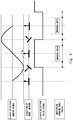
- Figs. 6A and 6B show operations according to a reference example in configurations similar to those shown in Figs. 1 to 3 and 5 .
- the H-axis detection pulse signal ideally has a detection waveform with a constant period, i.e., a rectangular wave in which High and Low are repeated at regular intervals between edges (at regular intervals between a rising edge and a subsequent falling edge, or at regular intervals between a falling edge and a subsequent rising edge).
- the area between counter values 6 to 15 is set as the drawing area.
- the HSync for setting the drawing area has a waveform in which a rising edge corresponding to the timing of the counter value 6 and a falling edge corresponding to the timing of the counter value 15 are repeated in each of the forward and reverse lines.
- the drawing area for the projected image 300 which is drawn by a repetition of the forward line and the reverse line corresponds to an area A1.
- the H-axis detection pulse signal has a constant period and the HSync also has a constant period. Accordingly, no deviation occurs in the drawing position of the drawing area A1 in each line, so that the longitudinal lines in the vertical direction are aligned.
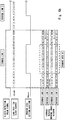
- FIGs. 7A and 7B show operations according to the reference example which is an example of configurations similar to those of Figs. 1 to 3 and 5 .
- the waveform of the frequency (edge interval) of the H-axis detection pulse signal is not constant but varies.
- the counter value of the clock counter varies in each edge interval.
- a forward line 1 corresponds to 20 counts
- a reverse line 2 corresponds to 18 counts
- a forward line 3 corresponds to 22 counts
- a reverse line 4 corresponds to 20 counts.
- the HSync for setting the drawing area has a waveform that repeatedly rises at the timing corresponding to the counter value 6 and falls at the timing corresponding to the counter value 15 in each of the forward and reverse lines in which the edge interval (the number of counts) varies.
- the drawing area for the projected image 300 which is drawn by a repetition of the forward line and the reverse line corresponds to an area A2.
- the period (edge interval) of the H-axis detection pulse signal varies and the period of the HSync also varies. Accordingly, a deviation occurs in the drawing position of the drawing area A2 in each line.
- drawing is performed by generating the timing waveform (HSync) for drawing based on the counter value of the H-axis detection pulse signal. Accordingly, when the number of counts in the forward line is different from the number of counts in the reverse line, a longitudinal line displacement occurs in the drawing area.
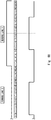
- FIGs. 8A and 8B show operations in the configurations of this embodiment illustrated in Figs. 1 to 5 .
- a line reference value is set as a reference for the edge interval (1 line) of the H-axis detection pulse signal.
- a value calculated from the line reference value is used as a start counter value from which counting is started in the next line.
- counting of the number of extra counts is continued in the next line, or counting is interrupted, and then counting is started from the same position as the counting start position corresponding to the line reference value.
- the line reference value represents the ideal deflection width of the MEMS mirror 224.
- the line reference value is an average value of the numbers of counts (or counter values) obtained by counting in a plurality of lines. For example, the number of edge intervals of the H-axis detection pulse signal from the MEMS mirror 224 is counted in a blanking area prior to the display of image data, and the values corresponding to eight lines are averaged and the average value thus obtained is set as the line reference value.
- the waveform of the frequency (edge interval) of the H-axis detection pulse signal is not constant but varies, like in Figs. 7A and 7B .
- the counter value of the clock counter clk_cnt
- the line reference value is set in such a manner that the start counter value in the next line is set at the same position as the count value corresponding to the line reference value.
- the deflection of the MEMS mirror 224 is less than the reference value
- the number of counts in, for example, the reverse line 2 is 18, which is smaller than the line reference value "20 counts", and the deflection of the MEMS mirror 224 is insufficient.
- the length at the left edge of the reverse line 2 in the horizontal direction is shorter than the line reference value.
- the counter value is smaller than the line reference value, the counter value is increased based on the difference between the counter value and the line reference value, to thereby shorten the interval from the edge of the next line to the drawing area. Therefore, the positions in the vertical direction of the counter values 6 to 15 in the reverse line 2 are the same as the positions in the vertical direction of the counter values 6 to 15 in the forward line 3.
- the deflection of the MEMS mirror 224 is greater than the reference value
- the number of counts in, for example, the forward line 3 is 22, which is greater than the line reference value "20 counts”
- the deflection of the MEMS mirror 224 is extremely large.
- the length at the right edge of the forward line 3 in the horizontal direction is longer than the line reference value.
- a counting start timing is delayed based on the difference between the counter value and the line reference value, thereby increasing the interval from the edge of the next line to the drawing area.
- the positions in the vertical direction of the counter values 6 to 15 in the forward line 3 are the same as the positions in the vertical direction of the counter values 6 to 15 in the reverse line 4.
- the counter value is not increased during a period of time corresponding to the number of counts of the difference value. Also in the next line, the count value "1" is maintained for a period of time corresponding to the counter value "four counts” in which the counter is interrupted, and then normal counting is started from the value "1". Alternatively, counting may be continued without interrupting the counter, until counting in the next line is started.
- the HSync for setting the drawing area has a waveform that repeatedly rises at the timing corresponding to the corrected counter value 6 and falls at the timing corresponding to the corrected counter value 15 in each of the forward and reverse lines in which the edge interval (the number of counts) varies.
- the drawing area for the projected image 300 which is drawn by a repetition of the forward line and the reverse line corresponds to an area A3.
- the counter is controlled based on the difference between the reference value and the edge interval of the H-axis detection pulse signal, so that the distance from the drawing area in the preceding line to the trailing edge thereof can be made equal to the distance from the leading edge of the next line to the drawing area. That is, in this embodiment, the count value is controlled based on the reference counter value and the count value from the detection pulse signal of the MEMS mirror so as to match the drawing areas in each longitudinal line, thereby making it possible to keep the drawing area range constant and eliminate a displacement of each longitudinal line.
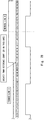
- the line reference value is determined based on the average value obtained by counting in a plurality of lines. For example, the average value of eight lines in one frame is set as the line reference value. However, if the line reference value is an odd number, drawing misalignment by one dot occurs. For this reason, it is preferable that the line reference value be constantly set to an even number.
- Fig. 9 shows an example in which the line reference value is set to an odd number.
- Fig. 9 shows an example in which the line reference value is 21 and the range from the counter value 6 to the counter value 15 is set as the drawing area.
- the drawing area for the projected image 300 which is drawn by a repetition of the forward line and the reverse line corresponds to an area A4.
- the line reference value is constantly set to an even number, to thereby prevent an occurrence of a displacement between the forward and reverse lines. For example, when the average value is 21, the reference value is set to 20 or 22.
- Fig. 10 is an example of functional blocks of the drawing position control unit 116.
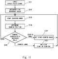
- Fig. 11 is an example of a flowchart for the drawing position control unit 116.
- the operation shown in Figs. 8A and 8B may be implemented by other configurations.
- the drawing position control unit 116 includes a counter 11, a line reference value setting unit 12, a drawing position determination unit 13, a line displacement determination unit 14, and a line displacement correction unit 15.
- the counter 11 is a counter that counts the edge intervals of the H-axis detection pulse signal.
- the counter 11 includes the clock counter shown in Fig. 8A and the pixel counter shown in Fig. 8B .
- the line reference value setting unit 12 sets a line reference value as a counter reference value in one line.
- the drawing position determination unit 13 determines the drawing position (drawing area) based on the value of the counter 11.
- the line displacement determination unit 14 compares the value of the counter 11 with the line reference value, and determines a displacement of each line.
- the line displacement correction unit 15 corrects the start counter value, or interrupts the counter, as shown in Figs. 8A and 8B , to correct the determined line displacement.
- the line reference value setting unit 12 first sets the line reference value. As described above, after the counter 11 counts the edge intervals of the H-axis detection pulse signal a plurality of times, the line reference value setting unit 12 obtains an average value of the counter values and sets the line reference value. In particular, the line reference value setting unit 12 sets the line reference value to an even number as described above.
- the counter 11 counts the scanning range of the MEMS mirror (S103).
- the counter 11 is synchronous with the internal clock and counts the edge intervals of the H-axis detection pulse signal by using the clock counter (clk cnt) and the pixel counter (pix cnt) as shown in Figs. 8A and 8B .
- the drawing position determination unit 13 determines the drawing position based on the counter value. For example, the drawing position determination unit 13 sets the area between the counter values 5 to 14 as the drawing area, and generates the HSync which repeatedly rises at the timing corresponding to the counter value 5 and falls at the timing corresponding to the counter value 14.
- the line displacement determination unit 14 compares the counter value with the line reference value (S105). When the counter value is equal to the line reference value, there is no line displacement, so that the counting and drawing position determination are carried out (S103, S104).
- the start counter value is set to correct the position of the drawing area based on the difference between the line reference value and the counter value (S106). After that, counting is started from the set start counter value, and the drawing position is determined (S103, S104).
- the operation of the MEMS mirror is detected by the piezoelectric films formed on the optical scanner, and the drawing position is corrected based on the difference between the detected operation range and the reference range.
- a deviation in the drawing position which is caused by a change in the detection waveform due to a variation in the operation of the MEMS mirror is corrected and the drawing area is constantly set at a certain location, thereby preventing drawing misalignment in each line.
- the count value for setting the drawing position is set to be constant with respect to the reference, instead of setting the count value to be always constant, thereby eliminating the misalignment of the drawing position in each line and preventing drawing misalignment.
Claims (4)
- Dispositif d'affichage d'image (100) comprenant :une unité de source de lumière (200) configurée pour émettre un faisceau de lumière ;une unité de balayage (220) configurée pour réfléchir le faisceau de lumière et pour répéter une opération de va-et-vient dans une direction de balayage prédéterminée ;une unité de détection de balayage (202) configurée pour détecter une plage de fonctionnement de l'unité de balayage (220) dans chaque ligne de balayage vers l'avant ou vers l'arrière de l'opération de va-et-vient ; la détection d'une plage de fonctionnement consistant à générer un signal d'impulsion de détection ayant des fronts d'impulsion situés selon la déflexion angulaire minimale et maximale de l'unité de balayage ;un compteur (11) configuré pour compter la plage de fonctionnement détectée en se basant sur une horloge ;une unité de détermination de position d'affichage (116) configurée pour déterminer une position d'affichage d'image dans chaque ligne de balayage en se basant sur une différence entre la plage de fonctionnement détectée et une plage de référence ;une unité de détermination de position de dessin (13) qui détermine la position de dessin en se basant sur la valeur de compteur ; la valeur de compteur pour définir la position de dessin étant fixée de sorte à être constante ;
etune unité d'excitation de source de lumière (140) configurée pour exciter l'unité de source de lumière (200) en se basant sur des données d'image à un moment correspondant à la position d'affichage d'image déterminée et à la position de dessin;caractérisé en ce que :lorsqu'une valeur de compteur obtenue par comptage pendant la plage de fonctionnement détectée par le compteur (11) est plus petite qu'une valeur de compteur correspondant à la plage de référence qui est une plage de fonctionnement idéale, l'unité de détermination de position d'affichage (116) écourte un intervalle allant d'un point de début de fonctionnement de l'unité de balayage (220) dans une ligne de balayage suivante à la position d'affichage d'image en augmentant une valeur de comptage de début du compteur (11) dans la ligne de balayage suivante en se basant sur la différence entre la valeur de compteur de la plage de fonctionnement détectée et la valeur de compteur correspondant à la plage de référence, etlorsqu'une valeur de compteur obtenue par comptage pendant la plage de fonctionnement détectée par le compteur (11) est plus importante qu'une valeur de compteur correspondant à la plage de référence qui est une plage de fonctionnement idéale, l'unité de détermination de position d'affichage (116) augmente l'intervalle allant du point de début de fonctionnement de l'unité de balayage (220) dans la ligne de balayage suivante à la position d'affichage d'image en retardant un moment de début de comptage du compteur (11) dans la ligne de balayage suivante en se basant sur la différence entre la valeur de compteur de la plage de fonctionnement détectée et la valeur de compteur correspondant à la plage de référence. - Dispositif d'affichage d'image (100) selon la revendication 1, dans lequel l'unité de détermination de position d'affichage (116) fixe la plage de référence en se basant sur une moyenne d'une pluralité de plages de fonctionnement détectées.
- Dispositif d'affichage d'image (100) selon la revendication 1 ou 2, dans lequel l'unité de détermination de position d'affichage (116) fixe la plage de référence de telle manière qu'une valeur de comptage obtenue en comptant la plage de fonctionnement en se basant sur une horloge devienne un nombre pair.
- Procédé de commande d'un dispositif d'affichage d'image (100), le dispositif d'affichage d'image (100) comprenant : une unité de source de lumière (200) configurée pour émettre un faisceau de lumière ; et une unité de balayage (220) configurée pour réfléchir le faisceau de lumière et pour répéter une opération de va-et-vient dans une direction de balayage prédéterminée, le procédé de commande consistant :à détecter une plage de fonctionnement de l'unité de balayage (220) dans chaque ligne de balayage vers l'avant ou vers l'arrière de l'opération de va-et-vient ; la détection d'une plage de fonctionnement consistant à générer un signal d'impulsion de détection ayant des fronts d'impulsion situés selon la déflexion angulaire minimale et maximale de l'unité de balayage ;à compter la plage de fonctionnement détectée en se basant sur une horloge ;à déterminer une position d'affichage d'image dans chaque ligne de balayage en se basant sur une différence entre la plage de fonctionnement détectée et une plage de référence ;à déterminer la position de dessin en se basant sur la valeur de compteur ; la valeur de compteur pour définir la position de dessin étant fixée de sorte à être constante ; età exciter l'unité de source de lumière (200) en se basant sur des données d'image à un moment correspondant à la position d'affichage d'image déterminée et à la position de dessin ;caractérisé par :lorsqu'une valeur de compteur obtenue par comptage pendant la plage de fonctionnement détectée est plus petite qu'une valeur de compteur correspondant à la plage de référence qui est une plage de fonctionnement idéale, lors de la détermination de la position d'affichage d'image, l'écourtement d'un intervalle allant d'un point de début de fonctionnement de l'unité de balayage (220) dans une ligne de balayage suivante à la position d'affichage d'image en augmentant une valeur de comptage de début dans la ligne de balayage suivante en se basant sur la différence entre la valeur de compteur de la plage de fonctionnement détectée et la valeur de compteur correspondant à la plage de référence, etlorsqu'une valeur de compteur obtenue par comptage pendant la plage de fonctionnement détectée est plus importante qu'une valeur de compteur correspondant à la plage de référence, lors de la détermination de la position d'affichage d'image qui est une plage de fonctionnement idéale, l'augmentation de l'intervalle allant du point de début de fonctionnement de l'unité de balayage (220) dans la ligne de balayage suivante à la position d'affichage d'image en retardant un moment de début de comptage dans la ligne de balayage suivante en se basant sur la différence entre la valeur de compteur de la plage de fonctionnement détectée et la valeur de compteur correspondant à la plage de référence.
Applications Claiming Priority (2)
| Application Number | Priority Date | Filing Date | Title |
|---|---|---|---|
| JP2013260396A JP6090147B2 (ja) | 2013-12-17 | 2013-12-17 | 画像表示装置及びその制御方法 |
| PCT/JP2014/003493 WO2015092948A1 (fr) | 2013-12-17 | 2014-07-01 | Dispositif d'affichage d'images et son procédé de commande |
Publications (3)
| Publication Number | Publication Date |
|---|---|
| EP3086548A1 EP3086548A1 (fr) | 2016-10-26 |
| EP3086548A4 EP3086548A4 (fr) | 2016-12-21 |
| EP3086548B1 true EP3086548B1 (fr) | 2019-10-16 |
Family
ID=53402339
Family Applications (1)
| Application Number | Title | Priority Date | Filing Date |
|---|---|---|---|
| EP14870909.0A Active EP3086548B1 (fr) | 2013-12-17 | 2014-07-01 | Dispositif d'affichage d'images et son procédé de commande |
Country Status (4)
| Country | Link |
|---|---|
| US (1) | US20160286185A1 (fr) |
| EP (1) | EP3086548B1 (fr) |
| JP (1) | JP6090147B2 (fr) |
| WO (1) | WO2015092948A1 (fr) |
Families Citing this family (8)
| Publication number | Priority date | Publication date | Assignee | Title |
|---|---|---|---|---|
| JP6269446B2 (ja) * | 2014-11-10 | 2018-01-31 | 株式会社Jvcケンウッド | 画像表示装置及びその制御方法 |
| JP6978659B2 (ja) * | 2016-12-21 | 2021-12-08 | ミツミ電機株式会社 | 画像投影装置および補償方法 |
| JP6350685B2 (ja) * | 2017-01-20 | 2018-07-04 | 株式会社Jvcケンウッド | 画像表示装置及びその制御方法 |
| JP6365698B2 (ja) * | 2017-01-20 | 2018-08-01 | 株式会社Jvcケンウッド | 画像表示装置及びその制御方法 |
| DE102017218670A1 (de) * | 2017-10-19 | 2019-04-25 | Robert Bosch Gmbh | Mikromechanische Mikrospiegelanordnung und entsprechendes Betriebsverfahren |
| JP7025634B2 (ja) * | 2017-11-01 | 2022-02-25 | ミツミ電機株式会社 | 画像投影装置及び画像投影方法 |
| JP6753449B2 (ja) | 2017-11-24 | 2020-09-09 | 株式会社村田製作所 | 走査反射器システム |
| JP6870699B2 (ja) * | 2018-05-03 | 2021-05-12 | 株式会社村田製作所 | 拡大された画像領域を備える走査光学デバイス |
Family Cites Families (10)
| Publication number | Priority date | Publication date | Assignee | Title |
|---|---|---|---|---|
| JP3265854B2 (ja) * | 1994-09-28 | 2002-03-18 | ミノルタ株式会社 | 画像出力装置 |
| US7302174B2 (en) * | 2003-12-31 | 2007-11-27 | Symbol Technologies, Inc. | Method and apparatus for capturing images using a color laser projection display |
| JP2007025522A (ja) | 2005-07-21 | 2007-02-01 | Seiko Epson Corp | 画像表示装置及び画像表示装置の制御方法 |
| US20070115440A1 (en) * | 2005-11-21 | 2007-05-24 | Microvision, Inc. | Projection display with screen compensation |
| US20080001850A1 (en) * | 2006-06-06 | 2008-01-03 | Mark Champion | Beam scanner with reduced phase error |
| US8842352B2 (en) * | 2006-08-17 | 2014-09-23 | Texas Instruments Incorporated | Method to improve scan-line alignment by adjusting the pixel rate |
| JP5393043B2 (ja) * | 2008-03-14 | 2014-01-22 | キヤノン株式会社 | 画像表示装置、画像表示方法 |
| JP2010266824A (ja) * | 2009-05-18 | 2010-11-25 | Seiko Epson Corp | 画像表示装置 |
| JP2013072982A (ja) * | 2011-09-27 | 2013-04-22 | Nec Corp | 蛍光体スクリーンおよびそれを用いた走査型表示装置 |
| JP2013140224A (ja) * | 2011-12-28 | 2013-07-18 | Jvc Kenwood Corp | 画像表示装置、画像表示装置の制御方法、および、情報出力装置 |
-
2013
- 2013-12-17 JP JP2013260396A patent/JP6090147B2/ja active Active
-
2014
- 2014-07-01 WO PCT/JP2014/003493 patent/WO2015092948A1/fr active Application Filing
- 2014-07-01 EP EP14870909.0A patent/EP3086548B1/fr active Active
-
2016
- 2016-06-03 US US15/173,282 patent/US20160286185A1/en not_active Abandoned
Non-Patent Citations (1)
| Title |
|---|
| None * |
Also Published As
| Publication number | Publication date |
|---|---|
| WO2015092948A1 (fr) | 2015-06-25 |
| JP6090147B2 (ja) | 2017-03-08 |
| EP3086548A1 (fr) | 2016-10-26 |
| JP2015118181A (ja) | 2015-06-25 |
| EP3086548A4 (fr) | 2016-12-21 |
| US20160286185A1 (en) | 2016-09-29 |
Similar Documents
| Publication | Publication Date | Title |
|---|---|---|
| EP3086548B1 (fr) | Dispositif d'affichage d'images et son procédé de commande | |
| US9894335B2 (en) | Image display device and control method thereof | |
| US8058633B2 (en) | Pulse width modulation signal generating device, image display apparatus including pulse width modulation signal generating device, and pulse width modulation signal generating method | |
| US7978387B2 (en) | Laser projector | |
| US8643923B2 (en) | Optical scanning device, optical scanning method, program, and image display device | |
| US20100079683A1 (en) | Display apparatus | |
| US9251730B2 (en) | Image display apparatus and image scanning apparatus | |
| JP2007093644A (ja) | 光走査型ディスプレイ | |
| JP2009198988A (ja) | 画像表示装置 | |
| WO2014103462A1 (fr) | Dispositif d'affichage d'images, procédé d'affichage d'images et programme | |
| JP2018010100A (ja) | レーザ投射表示装置 | |
| EP3349441A2 (fr) | Appareil de projection d'images et procédé de compensation | |
| US20190235229A1 (en) | Mems control circuit and projector | |
| KR20140000667A (ko) | 화상 표시 장치 | |
| JP6365698B2 (ja) | 画像表示装置及びその制御方法 | |
| JP6350685B2 (ja) | 画像表示装置及びその制御方法 | |
| US20170248781A1 (en) | Image drawing device and image drawing method | |
| JP2010266824A (ja) | 画像表示装置 | |
| JP2002002015A (ja) | 画像形成における同期信号発生方法及びその装置 | |
| JP4998291B2 (ja) | 光走査装置 | |
| JP2011133560A (ja) | 光走査型ディスプレイ |
Legal Events
| Date | Code | Title | Description |
|---|---|---|---|
| PUAI | Public reference made under article 153(3) epc to a published international application that has entered the european phase |
Free format text: ORIGINAL CODE: 0009012 |
|
| 17P | Request for examination filed |
Effective date: 20160607 |
|
| AK | Designated contracting states |
Kind code of ref document: A1 Designated state(s): AL AT BE BG CH CY CZ DE DK EE ES FI FR GB GR HR HU IE IS IT LI LT LU LV MC MK MT NL NO PL PT RO RS SE SI SK SM TR |
|
| AX | Request for extension of the european patent |
Extension state: BA ME |
|
| A4 | Supplementary search report drawn up and despatched |
Effective date: 20161122 |
|
| RIC1 | Information provided on ipc code assigned before grant |
Ipc: G02B 26/10 20060101ALI20161116BHEP Ipc: H04N 5/74 20060101AFI20161116BHEP Ipc: H04N 3/08 20060101ALI20161116BHEP |
|
| RIC1 | Information provided on ipc code assigned before grant |
Ipc: G02B 26/10 20060101ALI20170213BHEP Ipc: H04N 5/74 20060101AFI20170213BHEP Ipc: H04N 3/08 20060101ALI20170213BHEP |
|
| DAX | Request for extension of the european patent (deleted) | ||
| RIN1 | Information on inventor provided before grant (corrected) |
Inventor name: OOHARA, TATSUYA |
|
| STAA | Information on the status of an ep patent application or granted ep patent |
Free format text: STATUS: EXAMINATION IS IN PROGRESS |
|
| 17Q | First examination report despatched |
Effective date: 20180720 |
|
| 17Q | First examination report despatched |
Effective date: 20180727 |
|
| GRAP | Despatch of communication of intention to grant a patent |
Free format text: ORIGINAL CODE: EPIDOSNIGR1 |
|
| STAA | Information on the status of an ep patent application or granted ep patent |
Free format text: STATUS: GRANT OF PATENT IS INTENDED |
|
| INTG | Intention to grant announced |
Effective date: 20190621 |
|
| GRAS | Grant fee paid |
Free format text: ORIGINAL CODE: EPIDOSNIGR3 |
|
| GRAA | (expected) grant |
Free format text: ORIGINAL CODE: 0009210 |
|
| STAA | Information on the status of an ep patent application or granted ep patent |
Free format text: STATUS: THE PATENT HAS BEEN GRANTED |
|
| AK | Designated contracting states |
Kind code of ref document: B1 Designated state(s): AL AT BE BG CH CY CZ DE DK EE ES FI FR GB GR HR HU IE IS IT LI LT LU LV MC MK MT NL NO PL PT RO RS SE SI SK SM TR |
|
| REG | Reference to a national code |
Ref country code: GB Ref legal event code: FG4D |
|
| REG | Reference to a national code |
Ref country code: CH Ref legal event code: EP |
|
| REG | Reference to a national code |
Ref country code: DE Ref legal event code: R096 Ref document number: 602014055405 Country of ref document: DE |
|
| REG | Reference to a national code |
Ref country code: IE Ref legal event code: FG4D |
|
| REG | Reference to a national code |
Ref country code: AT Ref legal event code: REF Ref document number: 1192464 Country of ref document: AT Kind code of ref document: T Effective date: 20191115 |
|
| REG | Reference to a national code |
Ref country code: NL Ref legal event code: MP Effective date: 20191016 |
|
| REG | Reference to a national code |
Ref country code: LT Ref legal event code: MG4D |
|
| REG | Reference to a national code |
Ref country code: AT Ref legal event code: MK05 Ref document number: 1192464 Country of ref document: AT Kind code of ref document: T Effective date: 20191016 |
|
| PG25 | Lapsed in a contracting state [announced via postgrant information from national office to epo] |
Ref country code: SE Free format text: LAPSE BECAUSE OF FAILURE TO SUBMIT A TRANSLATION OF THE DESCRIPTION OR TO PAY THE FEE WITHIN THE PRESCRIBED TIME-LIMIT Effective date: 20191016 Ref country code: LV Free format text: LAPSE BECAUSE OF FAILURE TO SUBMIT A TRANSLATION OF THE DESCRIPTION OR TO PAY THE FEE WITHIN THE PRESCRIBED TIME-LIMIT Effective date: 20191016 Ref country code: PT Free format text: LAPSE BECAUSE OF FAILURE TO SUBMIT A TRANSLATION OF THE DESCRIPTION OR TO PAY THE FEE WITHIN THE PRESCRIBED TIME-LIMIT Effective date: 20200217 Ref country code: BG Free format text: LAPSE BECAUSE OF FAILURE TO SUBMIT A TRANSLATION OF THE DESCRIPTION OR TO PAY THE FEE WITHIN THE PRESCRIBED TIME-LIMIT Effective date: 20200116 Ref country code: FI Free format text: LAPSE BECAUSE OF FAILURE TO SUBMIT A TRANSLATION OF THE DESCRIPTION OR TO PAY THE FEE WITHIN THE PRESCRIBED TIME-LIMIT Effective date: 20191016 Ref country code: GR Free format text: LAPSE BECAUSE OF FAILURE TO SUBMIT A TRANSLATION OF THE DESCRIPTION OR TO PAY THE FEE WITHIN THE PRESCRIBED TIME-LIMIT Effective date: 20200117 Ref country code: NO Free format text: LAPSE BECAUSE OF FAILURE TO SUBMIT A TRANSLATION OF THE DESCRIPTION OR TO PAY THE FEE WITHIN THE PRESCRIBED TIME-LIMIT Effective date: 20200116 Ref country code: PL Free format text: LAPSE BECAUSE OF FAILURE TO SUBMIT A TRANSLATION OF THE DESCRIPTION OR TO PAY THE FEE WITHIN THE PRESCRIBED TIME-LIMIT Effective date: 20191016 Ref country code: AT Free format text: LAPSE BECAUSE OF FAILURE TO SUBMIT A TRANSLATION OF THE DESCRIPTION OR TO PAY THE FEE WITHIN THE PRESCRIBED TIME-LIMIT Effective date: 20191016 Ref country code: NL Free format text: LAPSE BECAUSE OF FAILURE TO SUBMIT A TRANSLATION OF THE DESCRIPTION OR TO PAY THE FEE WITHIN THE PRESCRIBED TIME-LIMIT Effective date: 20191016 Ref country code: LT Free format text: LAPSE BECAUSE OF FAILURE TO SUBMIT A TRANSLATION OF THE DESCRIPTION OR TO PAY THE FEE WITHIN THE PRESCRIBED TIME-LIMIT Effective date: 20191016 |
|
| PG25 | Lapsed in a contracting state [announced via postgrant information from national office to epo] |
Ref country code: HR Free format text: LAPSE BECAUSE OF FAILURE TO SUBMIT A TRANSLATION OF THE DESCRIPTION OR TO PAY THE FEE WITHIN THE PRESCRIBED TIME-LIMIT Effective date: 20191016 Ref country code: IS Free format text: LAPSE BECAUSE OF FAILURE TO SUBMIT A TRANSLATION OF THE DESCRIPTION OR TO PAY THE FEE WITHIN THE PRESCRIBED TIME-LIMIT Effective date: 20200224 Ref country code: RS Free format text: LAPSE BECAUSE OF FAILURE TO SUBMIT A TRANSLATION OF THE DESCRIPTION OR TO PAY THE FEE WITHIN THE PRESCRIBED TIME-LIMIT Effective date: 20191016 |
|
| PG25 | Lapsed in a contracting state [announced via postgrant information from national office to epo] |
Ref country code: AL Free format text: LAPSE BECAUSE OF FAILURE TO SUBMIT A TRANSLATION OF THE DESCRIPTION OR TO PAY THE FEE WITHIN THE PRESCRIBED TIME-LIMIT Effective date: 20191016 |
|
| REG | Reference to a national code |
Ref country code: DE Ref legal event code: R097 Ref document number: 602014055405 Country of ref document: DE |
|
| PG2D | Information on lapse in contracting state deleted |
Ref country code: IS |
|
| PG25 | Lapsed in a contracting state [announced via postgrant information from national office to epo] |
Ref country code: EE Free format text: LAPSE BECAUSE OF FAILURE TO SUBMIT A TRANSLATION OF THE DESCRIPTION OR TO PAY THE FEE WITHIN THE PRESCRIBED TIME-LIMIT Effective date: 20191016 Ref country code: CZ Free format text: LAPSE BECAUSE OF FAILURE TO SUBMIT A TRANSLATION OF THE DESCRIPTION OR TO PAY THE FEE WITHIN THE PRESCRIBED TIME-LIMIT Effective date: 20191016 Ref country code: RO Free format text: LAPSE BECAUSE OF FAILURE TO SUBMIT A TRANSLATION OF THE DESCRIPTION OR TO PAY THE FEE WITHIN THE PRESCRIBED TIME-LIMIT Effective date: 20191016 Ref country code: ES Free format text: LAPSE BECAUSE OF FAILURE TO SUBMIT A TRANSLATION OF THE DESCRIPTION OR TO PAY THE FEE WITHIN THE PRESCRIBED TIME-LIMIT Effective date: 20191016 Ref country code: DK Free format text: LAPSE BECAUSE OF FAILURE TO SUBMIT A TRANSLATION OF THE DESCRIPTION OR TO PAY THE FEE WITHIN THE PRESCRIBED TIME-LIMIT Effective date: 20191016 Ref country code: IS Free format text: LAPSE BECAUSE OF FAILURE TO SUBMIT A TRANSLATION OF THE DESCRIPTION OR TO PAY THE FEE WITHIN THE PRESCRIBED TIME-LIMIT Effective date: 20200216 |
|
| PLBE | No opposition filed within time limit |
Free format text: ORIGINAL CODE: 0009261 |
|
| STAA | Information on the status of an ep patent application or granted ep patent |
Free format text: STATUS: NO OPPOSITION FILED WITHIN TIME LIMIT |
|
| PG25 | Lapsed in a contracting state [announced via postgrant information from national office to epo] |
Ref country code: SM Free format text: LAPSE BECAUSE OF FAILURE TO SUBMIT A TRANSLATION OF THE DESCRIPTION OR TO PAY THE FEE WITHIN THE PRESCRIBED TIME-LIMIT Effective date: 20191016 Ref country code: IT Free format text: LAPSE BECAUSE OF FAILURE TO SUBMIT A TRANSLATION OF THE DESCRIPTION OR TO PAY THE FEE WITHIN THE PRESCRIBED TIME-LIMIT Effective date: 20191016 Ref country code: SK Free format text: LAPSE BECAUSE OF FAILURE TO SUBMIT A TRANSLATION OF THE DESCRIPTION OR TO PAY THE FEE WITHIN THE PRESCRIBED TIME-LIMIT Effective date: 20191016 |
|
| 26N | No opposition filed |
Effective date: 20200717 |
|
| PG25 | Lapsed in a contracting state [announced via postgrant information from national office to epo] |
Ref country code: SI Free format text: LAPSE BECAUSE OF FAILURE TO SUBMIT A TRANSLATION OF THE DESCRIPTION OR TO PAY THE FEE WITHIN THE PRESCRIBED TIME-LIMIT Effective date: 20191016 |
|
| PG25 | Lapsed in a contracting state [announced via postgrant information from national office to epo] |
Ref country code: MC Free format text: LAPSE BECAUSE OF FAILURE TO SUBMIT A TRANSLATION OF THE DESCRIPTION OR TO PAY THE FEE WITHIN THE PRESCRIBED TIME-LIMIT Effective date: 20191016 |
|
| REG | Reference to a national code |
Ref country code: CH Ref legal event code: PL |
|
| REG | Reference to a national code |
Ref country code: BE Ref legal event code: MM Effective date: 20200731 |
|
| PG25 | Lapsed in a contracting state [announced via postgrant information from national office to epo] |
Ref country code: CH Free format text: LAPSE BECAUSE OF NON-PAYMENT OF DUE FEES Effective date: 20200731 Ref country code: IE Free format text: LAPSE BECAUSE OF NON-PAYMENT OF DUE FEES Effective date: 20200701 Ref country code: FR Free format text: LAPSE BECAUSE OF NON-PAYMENT OF DUE FEES Effective date: 20200731 Ref country code: LI Free format text: LAPSE BECAUSE OF NON-PAYMENT OF DUE FEES Effective date: 20200731 Ref country code: LU Free format text: LAPSE BECAUSE OF NON-PAYMENT OF DUE FEES Effective date: 20200701 |
|
| PG25 | Lapsed in a contracting state [announced via postgrant information from national office to epo] |
Ref country code: BE Free format text: LAPSE BECAUSE OF NON-PAYMENT OF DUE FEES Effective date: 20200731 |
|
| PG25 | Lapsed in a contracting state [announced via postgrant information from national office to epo] |
Ref country code: TR Free format text: LAPSE BECAUSE OF FAILURE TO SUBMIT A TRANSLATION OF THE DESCRIPTION OR TO PAY THE FEE WITHIN THE PRESCRIBED TIME-LIMIT Effective date: 20191016 Ref country code: MT Free format text: LAPSE BECAUSE OF FAILURE TO SUBMIT A TRANSLATION OF THE DESCRIPTION OR TO PAY THE FEE WITHIN THE PRESCRIBED TIME-LIMIT Effective date: 20191016 Ref country code: CY Free format text: LAPSE BECAUSE OF FAILURE TO SUBMIT A TRANSLATION OF THE DESCRIPTION OR TO PAY THE FEE WITHIN THE PRESCRIBED TIME-LIMIT Effective date: 20191016 |
|
| PG25 | Lapsed in a contracting state [announced via postgrant information from national office to epo] |
Ref country code: MK Free format text: LAPSE BECAUSE OF FAILURE TO SUBMIT A TRANSLATION OF THE DESCRIPTION OR TO PAY THE FEE WITHIN THE PRESCRIBED TIME-LIMIT Effective date: 20191016 |
|
| PGFP | Annual fee paid to national office [announced via postgrant information from national office to epo] |
Ref country code: GB Payment date: 20230601 Year of fee payment: 10 |
|
| PGFP | Annual fee paid to national office [announced via postgrant information from national office to epo] |
Ref country code: DE Payment date: 20230531 Year of fee payment: 10 |