WO2015092948A1 - Dispositif d'affichage d'images et son procédé de commande - Google Patents
Dispositif d'affichage d'images et son procédé de commande Download PDFInfo
- Publication number
- WO2015092948A1 WO2015092948A1 PCT/JP2014/003493 JP2014003493W WO2015092948A1 WO 2015092948 A1 WO2015092948 A1 WO 2015092948A1 JP 2014003493 W JP2014003493 W JP 2014003493W WO 2015092948 A1 WO2015092948 A1 WO 2015092948A1
- Authority
- WO
- WIPO (PCT)
- Prior art keywords
- image display
- counter
- line
- unit
- range
- Prior art date
Links
Images


Classifications
-
- G—PHYSICS
- G02—OPTICS
- G02B—OPTICAL ELEMENTS, SYSTEMS OR APPARATUS
- G02B26/00—Optical devices or arrangements for the control of light using movable or deformable optical elements
- G02B26/08—Optical devices or arrangements for the control of light using movable or deformable optical elements for controlling the direction of light
- G02B26/0816—Optical devices or arrangements for the control of light using movable or deformable optical elements for controlling the direction of light by means of one or more reflecting elements
- G02B26/0833—Optical devices or arrangements for the control of light using movable or deformable optical elements for controlling the direction of light by means of one or more reflecting elements the reflecting element being a micromechanical device, e.g. a MEMS mirror, DMD
- G02B26/0858—Optical devices or arrangements for the control of light using movable or deformable optical elements for controlling the direction of light by means of one or more reflecting elements the reflecting element being a micromechanical device, e.g. a MEMS mirror, DMD the reflecting means being moved or deformed by piezoelectric means
-
- H—ELECTRICITY
- H04—ELECTRIC COMMUNICATION TECHNIQUE
- H04N—PICTORIAL COMMUNICATION, e.g. TELEVISION
- H04N9/00—Details of colour television systems
- H04N9/12—Picture reproducers
- H04N9/31—Projection devices for colour picture display, e.g. using electronic spatial light modulators [ESLM]
- H04N9/3179—Video signal processing therefor
- H04N9/3185—Geometric adjustment, e.g. keystone or convergence
-
- G—PHYSICS
- G02—OPTICS
- G02B—OPTICAL ELEMENTS, SYSTEMS OR APPARATUS
- G02B26/00—Optical devices or arrangements for the control of light using movable or deformable optical elements
- G02B26/08—Optical devices or arrangements for the control of light using movable or deformable optical elements for controlling the direction of light
- G02B26/10—Scanning systems
- G02B26/101—Scanning systems with both horizontal and vertical deflecting means, e.g. raster or XY scanners
-
- G—PHYSICS
- G02—OPTICS
- G02B—OPTICAL ELEMENTS, SYSTEMS OR APPARATUS
- G02B27/00—Optical systems or apparatus not provided for by any of the groups G02B1/00 - G02B26/00, G02B30/00
- G02B27/01—Head-up displays
-
- H—ELECTRICITY
- H04—ELECTRIC COMMUNICATION TECHNIQUE
- H04N—PICTORIAL COMMUNICATION, e.g. TELEVISION
- H04N9/00—Details of colour television systems
- H04N9/12—Picture reproducers
- H04N9/31—Projection devices for colour picture display, e.g. using electronic spatial light modulators [ESLM]
- H04N9/3129—Projection devices for colour picture display, e.g. using electronic spatial light modulators [ESLM] scanning a light beam on the display screen
- H04N9/3135—Driving therefor
-
- H—ELECTRICITY
- H04—ELECTRIC COMMUNICATION TECHNIQUE
- H04N—PICTORIAL COMMUNICATION, e.g. TELEVISION
- H04N9/00—Details of colour television systems
- H04N9/12—Picture reproducers
- H04N9/31—Projection devices for colour picture display, e.g. using electronic spatial light modulators [ESLM]
- H04N9/3191—Testing thereof
- H04N9/3194—Testing thereof including sensor feedback
-
- G—PHYSICS
- G02—OPTICS
- G02B—OPTICAL ELEMENTS, SYSTEMS OR APPARATUS
- G02B27/00—Optical systems or apparatus not provided for by any of the groups G02B1/00 - G02B26/00, G02B30/00
- G02B27/01—Head-up displays
- G02B27/0101—Head-up displays characterised by optical features
- G02B2027/014—Head-up displays characterised by optical features comprising information/image processing systems
-
- G—PHYSICS
- G02—OPTICS
- G02B—OPTICAL ELEMENTS, SYSTEMS OR APPARATUS
- G02B27/00—Optical systems or apparatus not provided for by any of the groups G02B1/00 - G02B26/00, G02B30/00
- G02B27/01—Head-up displays
- G02B27/0101—Head-up displays characterised by optical features
Definitions
- the present invention relates to an image display device and a control method thereof, and more specifically, to a laser scan type image display device and a control method thereof.
- a laser scan type image display device that projects and displays an image by reflecting and scanning laser light is known (for example, Patent Document 1).
- Laser scanning image display devices are used as HUDs (Head-Up-Displays), projectors, and the like that project and display images on windshields and combiners of automobiles.
- laser light is scanned by reflecting the laser light by an optical scanner having a mirror and reciprocally swinging the mirror of the optical scanner in the horizontal direction and the vertical direction.
- the reciprocation of the optical scanner may fluctuate due to vibrations or electrical influences, and in the conventional image display device, the image may be shifted and displayed for each scanning unit such as a horizontal line due to this fluctuation. There is a problem that there is.
- the present invention provides a light source unit that outputs a light beam, a scanning unit that reflects the light beam and repeats a reciprocating operation in a predetermined scanning direction, and the operation of the scanning unit for each scanning unit of the forward or backward path of the reciprocating operation.
- a scanning detection unit for detecting a range; a display position determining unit for determining an image display position for each scanning unit based on a deviation between the detected operation range and a reference range; and the determined image display position.
- an image display device comprising: a light source driving unit that drives the light source unit based on image data at a corresponding timing.
- a control method for an image display device comprising: a light source unit that outputs a light beam; and a scanning unit that reflects the light beam and repeats a reciprocating operation in a predetermined scanning direction.
- the operating range of the scanning unit is detected for each scanning unit of the forward path or the backward path, and the image display position is determined for each scanning unit based on the deviation between the detected operating range and the reference range.
- a method for controlling an image display device wherein the light source unit is driven based on image data at a timing corresponding to an image display position.
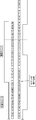
- FIG. 1 is a configuration diagram illustrating a configuration example of an image display device according to a first embodiment.
- 2 is a configuration diagram illustrating an example of a configuration of a horizontal scanner according to Embodiment 1.
- FIG. FIG. 10 is a configuration diagram illustrating another example of the configuration of the horizontal scanner according to the first embodiment.
- 1 is a block diagram illustrating a configuration example of an FPGA according to a first embodiment.
- 4 is a waveform diagram illustrating an example of signals used in the image display device according to Embodiment 1.
- FIG. 6 is an explanatory diagram for explaining an operation at the time of reciprocal scanning fluctuation according to the first embodiment.
- FIG. 6 is an explanatory diagram for explaining an operation at the time of reciprocal scanning fluctuation according to the first embodiment.
- 6 is an explanatory diagram for explaining an example of setting a line reference value according to Embodiment 1.
- FIG. 4 is a block diagram illustrating a configuration example of a drawing position control unit according to Embodiment 1.
- FIG. 4 is a flowchart illustrating an operation example of a drawing position control unit according to the first embodiment.
- FIG. 1 shows a configuration of an image display apparatus 100 according to the present embodiment.
- the image display device 100 is a laser scan type image display device that displays (draws) an image on a projection surface by reflecting laser light with an optical scanner and reciprocatingly scanning in a vertical direction and a horizontal direction.
- the image display device 100 projects and displays the projection image 300 on a projection surface that is an image display surface such as an automobile windshield or combiner.
- the image display apparatus 100 includes a video input unit 101, an FPGA (Field Programmable Gate Array) 110, a microcomputer 120, flash memories 131 and 132, a DDR (Double Data Rate) memory 133, a laser driver 140, a V An axis scanner driver 150, an H axis scanner driver 160, a comparator 170, an RGB laser diode 200, a vertical scanner 210, and a horizontal scanner 220 are provided.
- the vertical direction (vertical direction, Y direction) of the image to be displayed is also referred to as a V (Vertical) axis direction
- the horizontal direction (lateral direction, X direction) of the image is also referred to as an H (Horizontal) axis direction.
- the video input unit 101 receives video data to be displayed on the projection plane, and the input video data is sent to the FPGA 110.
- This video data includes three color signals of R (red), G (green), and B (blue).
- the video input unit 101 may receive a video generated by another device such as a car navigation device, or the video input unit 101 may generate video data.
- the FPGA 110 and the microcomputer 120 constitute the control unit 102 of the image display device 100 and perform various controls necessary for image display.
- the operations of the RGB laser diode 200, the vertical scanner 210, and the horizontal scanner 220 are controlled by the FPGA 110 and the microcomputer 120 via the laser driver 140, the V-axis scanner driver 150, and the H-axis scanner driver 160, and the projected image 300 is drawn.
- the control operations of the FPGA 110 and the microcomputer 120 may be realized by either hardware or software, or both.
- the FPGA 110 outputs RGB image data line by line based on the input video data, generates a V-axis drive signal for controlling the reciprocation of the vertical scanner 210, and generates the generated V-axis drive signal. Is output.
- the FPGA 110 sets and sets the image drawing position so as to suppress the image shift for each line based on the H-axis detection pulse signal of the horizontal scanner 220 obtained from the comparator 170. At this position, the laser driver 140 is driven to perform drawing.
- the microcomputer 120 generates an H-axis drive signal for controlling the reciprocation of the horizontal scanner 220, and outputs the generated H-axis drive signal.
- the flash memories 131 and 132 are nonvolatile storage units that store data and programs necessary for the operation of the FPGA 110 and the microcomputer 120, respectively.
- a DDR (Double Data Rate) memory 133 is a frame buffer that temporarily stores video data input to the FPGA 110.
- the DDR memory 133 may be DDR2, DDR3, or other SDRAM.
- the laser driver 140 drives the RGB laser diode 200 according to the image data supplied from the FPGA 110.
- the laser driver 140 is a light source driving unit that drives the RGB laser diode 200 based on image data at a timing corresponding to the image display position determined by the FPGA 110.
- the RGB laser diode 200 emits three colors of RGB laser light by driving the laser driver 140.
- the RGB laser diode 200 is a light source unit that outputs laser light that is a light beam.
- the V-axis scanner driver 150 reciprocates the vertical scanner 210 in accordance with the V-axis drive signal supplied from the FPGA 110.
- the H-axis scanner driver 160 drives the horizontal scanner 220 reciprocally according to the H-axis drive signal supplied from the microcomputer 120.
- the vertical scanner 210 or the horizontal scanner 220 is a scanning unit that repeats reciprocation in the vertical or horizontal direction.
- the vertical scanner 210 is an optical scanner that reflects the laser light emitted from the RGB laser diode 200 and reciprocates in the vertical direction by driving the V-axis scanner driver 150.
- the horizontal scanner 220 is an optical scanner that reflects the laser light emitted from the RGB laser diode 200 and reciprocates in the horizontal direction by driving the H-axis scanner driver 160.
- the horizontal scanner 220 includes a scanning detection unit 202 that detects a horizontal reciprocation, and outputs an H-axis detection analog signal indicating the detected reciprocation.
- the scanning detection unit 202 detects the operating range of the horizontal scanner 220 for each scanning unit that is a forward or backward line of a reciprocating operation.
- the horizontal scanner 220 reflects the laser light from the RGB laser diode 200, and the vertical scanner 210 further reflects the reflected light from the horizontal scanner 220, thereby drawing the projection image 300 on the projection surface.
- the vertical scanner 210 and the horizontal scanner 220 constitute an optical scanner 201 that reciprocates in the vertical and horizontal directions.
- the vertical scanner 210 and the horizontal scanner 220 may be a single two-axis (two-dimensional) optical scanner.
- the comparator 170 is a signal conversion unit that converts the H-axis detection analog signal output from the horizontal scanner 220 into an H-axis detection pulse signal that can be processed by the FPGA 110.
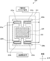
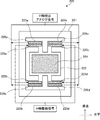
- FIGS. 2 and 3 are configuration examples of the horizontal scanner 220, and are front views of the horizontal scanner 220 as viewed from the mirror side. Note that the vertical scanner 210 may be configured similarly to the horizontal scanner 220.
- the optical scanner which is the horizontal scanner 220 (and the vertical scanner 210) is a MEMS element created by MEMS (Micro Electro Mechanical Systems) technology.
- the horizontal scanner 220 is formed by etching an SOI (Silicon On On Insulator) substrate including a piezoelectric film such as a PZT (lead zirconate titanate) film.
- the horizontal scanner 220 includes a frame body 221 constituting a frame of the main body, a swinging piece portion 222 supported in a state of being separated from the frame body 221 in the frame of the frame body 221, a frame Four L-shaped beam portions 223a to 223d that connect the inner edge of the body 221 and the swing piece 222, and a MEMS mirror 224 formed on the surface of the swing piece 222 are provided.
- the MEMS mirror 224 is formed by vapor-depositing a metal with high reflectivity (for example, Al or Au).
- the L-shaped beam portions 223a to 223d are connected to the swing piece 222 at a position close to the center in the horizontal direction of the swing piece 222, and the swing piece 222 and the MEMS mirror with the connecting portion as a swing axis. 224 can swing in the horizontal direction. It can be said that the L-shaped beam portions 223a to 223d constitute a torsion bar that supports the swing piece portion 222 in a swingable manner.
- the piezoelectric film has a laminated structure in which a piezoelectric film is sandwiched between a lower electrode and an upper electrode.
- driving piezoelectric films 225a and 225b to which an H-axis driving signal is supplied are arranged on the L-shaped beam portions 223a and 223b, respectively, and the L-shaped beam portion 223c facing the L-shaped beam portions 223a and 223b.
- detection piezoelectric films 226a and 226b for detecting the operation of the MEMS mirror 224 (the swing piece 222) are arranged, respectively.
- a pair of driving piezoelectric films and detecting piezoelectric films (225a and 226a, 225b and 226b, 225c and 226c, 225d and 226d) are arranged on the L-shaped beam portions 223a to 223d, respectively. Yes.
- the detection piezoelectric films 226a and 226b in FIG. 2 or the detection piezoelectric films 226a to 226d in FIG. 3 are the scanning detection unit 202, and detect and detect vibrations of the swing piece 222 and the MEMS mirror 224.
- An H-axis detection analog signal corresponding to vibration is output.
- An H-axis drive signal having a predetermined phase difference with respect to the H-axis detection analog signal obtained from the detection piezoelectric films 226a and 226b or 226a to 226d is fed back to the drive piezoelectric films 225a and 225b or 225a to 225d.
- the oscillating piece 222 and the MEMS mirror 224 can be driven to resonate.
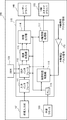
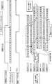
- FIG. 4 shows functional blocks of the FPGA 110 according to the present embodiment.
- the FPGA 110 includes an input interface 111, a DDR interface 112, an image processing unit 113, a video output unit 114, a PLL (Phase Locked Loop) 115, a drawing position control unit 116, and a V-axis drive processing unit 117. ing.
- PLL Phase Locked Loop
- the input interface 111 is an interface with the video input unit 101, receives the video data input from the video input unit 101, and outputs the received video data to the DDR interface 112.
- the DDR interface 112 is an interface with the DDR memory 133, temporarily stores the video data received by the input interface 111 in the DDR memory 133, and further extracts the video data stored in the DDR 133 according to the internal clock.
- the DDR interface 112 writes video data (image data) to the DDR memory 133 in units of frames, and reads each line in the horizontal direction included in one frame from the DDR memory 133 in synchronization with the internal clock.
- the DDR interface 112 reads image data in the order of forward addresses in the case of the forward path line to be drawn in the forward path, and The image data is read out in the order of the addresses in the reverse direction to rearrange the image data of the forward path and the backward path.
- the image processing unit 113 performs necessary image processing such as change of aspect ratio and bright control on the image data extracted from the DDR 133 by the DDR interface 112.
- the video output unit (image output unit) 114 outputs the image data processed by the image processing unit 113 to the laser driver 140.
- the video output unit 114 determines the drawing position using the drawing position clock (pixel clock), HSync (H axis synchronization signal), and VSync (V axis synchronization signal) generated from the H axis detection waveform and the V axis drive signal. Then, the image data is output line by line at the determined drawing position timing.
- the PLL 115 receives an external clock 180, generates an internal clock based on the external clock 180, and supplies the generated internal clock to each block.
- the drawing position control unit (clock generation unit) 116 generates a pixel clock based on the internal clock generated by the PLL 115 in order to synchronize laser drawing with the horizontal scanner 220.
- the pixel clock is a clock synchronized with a pixel counter described later.
- the drawing position control unit 116 generates pixel clocks HSync and VSync that determine the drawing position based on the H-axis detection pulse signal and the V-axis drive signal.
- the drawing position control unit 116 starts counting of the counter from the edge position of the H-axis detection pulse signal, and determines a drawing area based on the counted counter value.
- the drawing position control unit 116 is a display position determination unit that determines the image display position for each line based on the deviation between the operation range of the horizontal scanner 220 detected by the scan detection unit 202 and the reference range.
- the V-axis drive processing unit 117 generates a V-axis drive signal based on HSync and VSync, and outputs the generated V-axis drive signal to the V-axis scanner driver 150.
- VGA Video Graphics Graphics Array
- the vertical scanning frequency is 60 Hz
- the V-axis drive signal is output so that the vertical scanner 210 is swung in the vertical direction at 60 Hz.
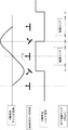
- FIG. 5 shows an example of the H-axis detection analog signal and the H-axis detection pulse signal according to the present embodiment.
- the H-axis detection analog signal is a waveform detected by one-side piezoelectric film (for example, 226a and 226b in FIG. 2 or 226a to 226d in FIG. 3) disposed in the horizontal scanner 220 that is driven on both sides in the horizontal direction. .
- the H-axis detection analog signal is an analog waveform corresponding to the direction of the MEMS mirror 224 of the horizontal scanner 220. For this reason, the H-axis detection analog signal cannot be processed by the FPGA 110 as it is. Therefore, in the present embodiment, the H-axis detection analog signal is converted into a pulsed rectangular wave using the comparator 170 or the like, and is input to the FPGA 110 as the H-axis detection pulse signal.
- the H-axis detection pulse signal is generated so that the edge comes to the position where the MEMS mirror 224 is swung by the maximum angle.
- the H-axis detection pulse signal is generated so as to repeat rising / falling for every minimum value (at the minimum peak) and maximum value (at the maximum peak) of the H-axis detection analog signal. Then, a horizontal drawing area is set in an area between edges sandwiched between edges of the H-axis pulse signal.
- an H-axis detection waveform (H-axis detection pulse signal) that is detected from the operation of the MEMS mirror 224 output from a detection circuit such as a piezoelectric film is taken into the FPGA 110 and the drawing timing is set. Used as a reference signal.
- the H-axis detection pulse signal also changes in the same manner. Since the FPGA 110 counts the edge interval of the H-axis detection pulse signal, the change in the frequency of the H-axis detection pulse signal causes a shift in the drawing timing due to a shift in the count number in the FPGA 110, and the projection to be drawn. This leads to a shift for each line of the image 300. In the present embodiment, this problem is improved as described below.
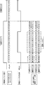
- FIGS. 6A and 6B show the operation of the reference example, which is an example having the same configuration as FIGS. 1 to 3 and FIG.
- the H-axis detection pulse signal always has a detection waveform with a constant period, that is, the same edge interval (interval between the rising edge and the next falling edge, the falling edge, This is a rectangular wave that repeats High / Low at an interval until the next rising edge).
- the FPGA 110 counts the edge interval of the H-axis detection pulse signal with an internal clock synchronized with the dot (pixel), and the H-axis detection pulse signal has a constant period, so the counter value of the clock counter (clk_cnt) is a constant value. It becomes.
- a counter value between 6 and 15 is set as a drawing area.
- HSync that sets the drawing area has a waveform that rises at the timing of the counter value 6 and repeats falling at the timing of the counter value 15 in each of the forward and return lines.
- the drawing area of the projection image 300 drawn by repeating the forward line and the backward line is the area A1.
- the H-axis detection pulse signal has a constant cycle and HSync also has a constant cycle
- the drawing position in the drawing area A1 is not shifted for each line, and the vertical vertical line is a straight line.
- FIGS. 7A and 7B show the operation of the reference example, which is an example having the same configuration as FIGS. 1 to 3 and FIG.
- the H-axis detection pulse signal when the operation of the MEMS mirror 224 is not constant, the H-axis detection pulse signal has a waveform in which the frequency (edge interval) is not constant but has changed.
- the counter value of the clock counter varies for each edge interval.
- the edge interval of the H-axis detection pulse signal is narrowed, so the counter value is small, and the MEMS mirror 224 is too much deviated from the ideal standard.
- the counter value becomes large.
- the forward line 1 is 20 counts
- the backward line 2 is 18 counts
- the forward line 3 is 22 counts
- the backward line 4 is 20 counts.
- the HSync for setting the drawing area rises at the timing of the counter value 6 for each of the forward and return lines where the edge interval (count number) varies, and the counter value 15 The waveform repeats falling at the timing.
- the drawing area of the projection image 300 drawn by repeating the forward line and the backward line is the area A2.
- the cycle (edge interval) of the H-axis detection pulse signal varies and the cycle of HSync also varies, so that the rendering position of the rendering area A2 is shifted for each line.
- the timing waveform (HSync) for drawing is generated and drawn on the basis of the counter value of the H-axis detection pulse signal, and drawing is performed when the count numbers in the forward line and the backward line are different. Deviation occurs in the vertical lines of the area.
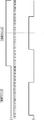
- FIGS. 8A and 8B show the operation in the configuration of the present embodiment described with reference to FIGS.
- a line reference value serving as a reference for the edge interval (one line) of the H-axis detection pulse signal is set.
- a value calculated from the line reference value is used as a start counter value for starting counting on the next line. If the counter value is larger than the line reference value, the extra count is continued on the next line, or the count is stopped, and the count is started from the same position as the start position of the line reference value.
- the line reference value is an ideal deflection width of the MEMS mirror 224, and here, is an average value of counts (or counter values) obtained by counting a plurality of lines. For example, the edge interval of the H-axis detection pulse signal from the MEMS mirror 224 is counted in the blanking area before image data display, and the line reference value is set by averaging eight lines.
- FIGS. 7A and 7B show waveforms in which the frequency (edge interval) of the H-axis detection pulse signal is not constant, as in FIGS. 7A and 7B.
- the counter value of the clock counter clk_cnt
- a line reference value is set, and the start counter value is set so that the start count when moving to the next line is the same position as the line reference value count.
- the return line 2 has 18 counts, which is smaller than the line reference value of 20 counts, and the MEMS mirror 224 does not have enough deflection.
- the left end in the horizontal direction is shorter than the line reference value.
- the start counter value of line 3 is assumed.
- the interval from the edge of the next line to the drawing area is shortened by increasing the counter value based on the difference between the counter value and the line reference value.
- the counter values 6 to 15 of the return line 2 and the counter values 6 to 15 of the forward line 3 are equal in the vertical direction.
- the outbound line 3 has 22 counts, which is larger than the line reference value of 20 counts, and the MEMS mirror 224 is swung too much.
- the right end in the horizontal direction is longer than the line reference value.
- the interval from the edge of the next line to the drawing area is lengthened by delaying the start of counting based on the difference between the counter value and the line reference value.
- the counter values 6 to 15 of the forward path line 3 and the counter values 6 to 15 of the return path line 4 are equal to each other in the vertical direction.
- the counter value is not advanced during the count of the difference value, and after moving to the next line, the count value is stopped for 1 count for 4 counts of the stopped count value. Start counting from 1. Further, the counting may be continued without stopping until the counting is started on the next line.
- HSync for setting the drawing area rises at the timing of the corrected counter value 6 for each of the forward and return lines where the edge interval (count number) fluctuates, and the timing of the corrected counter value 15 The waveform repeats falling at.
- the drawing area of the projected image 300 drawn by repeating the forward line and the backward line is the area A3.
- the drawing area is controlled by controlling the count value based on the counter value as a reference and the count value from the detection pulse signal of the MEMS mirror so that the drawing areas match in the vertical line.
- the range can be kept constant, and vertical line shifts can be eliminated.
- the line reference value is determined by the average value obtained by counting a plurality of lines. For example, an average value of 8 lines in one frame is set as a line reference value. However, if the line reference value is an odd number, drawing deviation of one dot occurs. Therefore, it is preferable to determine that the line reference value is always an even number.
- FIG. 9 shows an example in which the line reference value is set to an odd number.
- FIG. 9 shows an example in which the line reference value is 21 and the area between the counter values 6 to 15 is a drawing area.
- the drawing area of the projection image 300 drawn by repeating the forward path line and the backward path line is the area A4.
- the line reference value is set to an odd number as shown in FIG. 9, the drawing position on the forward line (counter values 6 to 15) and the drawing position on the backward line (counter values 6 to 15) are shifted by one dot, and the forward path And the return path becomes alternate. For this reason, in this embodiment, the line reference value is always set to an even number to prevent the deviation between the forward path and the backward path. For example, when the average value is 21, the reference value is set to 20 or 22.
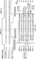
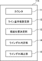
- FIG. 10 is an example of a functional block of the drawing position control unit 116
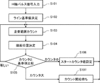
- FIG. 11 is an example of a flowchart of the drawing position control unit 116. Note that the operations in FIGS. 8A and 8B may be realized by other configurations.
- the drawing position control unit 116 includes a counter 11, a line reference value setting unit 12, a drawing position determination unit 13, a line deviation determination unit 14, and a line deviation correction unit 15.
- the counter 11 is a counter that counts the edge interval of the H-axis detection pulse signal.
- the counter 11 includes the clock counter and the pixel counter shown in FIGS. 8A and 8B.
- the line reference value setting unit 12 sets a line reference value to be a reference value for the counter of one line.
- the drawing position determination unit 13 determines a drawing position (drawing area) based on the value of the counter 11.
- the line deviation determination unit 14 compares the value of the counter 11 with the line reference value to determine line deviation.
- the line shift correction unit 15 corrects the start counter value and stops the counter as shown in FIGS. 8A and 8B.
- the line reference value setting unit 12 first sets a line reference value. As described above, after the counter 11 counts the edge interval of the H-axis detection pulse signal a plurality of times, the line reference value setting unit 12 obtains the average value of the counter values and sets the line reference value. In particular, the line reference value setting unit 12 sets the line reference value to be an even number as described above.
- the counter 11 counts the scanning range of the MEMS mirror (S103). In synchronization with the internal clock, the counter 11 counts the edge interval of the H-axis detection pulse signal by a clock counter (clk_cnt) and a pixel counter (pix_cnt) as shown in FIGS. 8A and 8B.
- a clock counter clk_cnt
- pix_cnt a pixel counter
- the drawing position determination unit 13 determines the drawing position based on the counter value. For example, the drawing position determination unit 13 sets between the counter values 5 to 14 as a drawing area, and generates HSync that rises at the timing of the counter value 5 and repeats the falling at the timing of the counter value 14.
- the line deviation determination unit 14 compares the counter value with the line reference value (S105). If the counter value is equal to the line reference value, there is no deviation in the line, so the count and the drawing position are determined as they are (S103, S104).
- the start counter value is set so as to correct the position of the drawing area based on the difference between the line reference value and the counter value as shown in FIGS. 8A and 8B (S106). . Thereafter, counting is started based on the set start counter value, and the drawing position is determined (S103, S104).
- the start of counting is waited so as to correct the position of the drawing area based on the difference between the counter value and the line reference value (S107). . Thereafter, the counting is started in accordance with the timing when there is no difference from the line reference value, and the drawing position is determined (S103, S104).
- the operation of the MEMS mirror is detected by the piezoelectric film provided in the optical scanner, and based on the deviation between the detected operation range and the reference range.
- the drawing position was corrected. Accordingly, the drawing position shift caused by the change in the detected waveform due to the fluctuation of the operation of the MEMS mirror is corrected, and the drawing shift for each line can be prevented by always setting the drawing area at a fixed location.
- the count value for setting the drawing position so as not to be always constant but constant with respect to the reference, it is possible to eliminate drawing position deviation for each line and prevent drawing deviation.
Abstract
La présente invention concerne un dispositif d'affichage d'images (100) comprenant une diode laser RGB (200) qui émet de la lumière laser, un scanner horizontal (220) qui reflète la lumière laser et réalise une opération de va-et-vient dans le sens horizontal, une unité de détection de balayage (202) qui détecte une plage de fonctionnement pour chaque ligne dans le sens horizontal, une unité de commande de position de rendu (116) qui détermine une position d'affichage d'images pour chaque ligne, sur la base d'une divergence entre la plage détectée du fonctionnement et une valeur de référence de ligne, et un circuit d'attaque de laser (140) qui commande la diode laser RGB (200) sur la base des données d'images, avec une temporisation correspondant à la position d'affichage d'image déterminée.
Priority Applications (2)
| Application Number | Priority Date | Filing Date | Title |
|---|---|---|---|
| EP14870909.0A EP3086548B1 (fr) | 2013-12-17 | 2014-07-01 | Dispositif d'affichage d'images et son procédé de commande |
| US15/173,282 US20160286185A1 (en) | 2013-12-17 | 2016-06-03 | Image display device and control method thereof |
Applications Claiming Priority (2)
| Application Number | Priority Date | Filing Date | Title |
|---|---|---|---|
| JP2013-260396 | 2013-12-17 | ||
| JP2013260396A JP6090147B2 (ja) | 2013-12-17 | 2013-12-17 | 画像表示装置及びその制御方法 |
Related Child Applications (1)
| Application Number | Title | Priority Date | Filing Date |
|---|---|---|---|
| US15/173,282 Continuation US20160286185A1 (en) | 2013-12-17 | 2016-06-03 | Image display device and control method thereof |
Publications (1)
| Publication Number | Publication Date |
|---|---|
| WO2015092948A1 true WO2015092948A1 (fr) | 2015-06-25 |
Family
ID=53402339
Family Applications (1)
| Application Number | Title | Priority Date | Filing Date |
|---|---|---|---|
| PCT/JP2014/003493 WO2015092948A1 (fr) | 2013-12-17 | 2014-07-01 | Dispositif d'affichage d'images et son procédé de commande |
Country Status (4)
| Country | Link |
|---|---|
| US (1) | US20160286185A1 (fr) |
| EP (1) | EP3086548B1 (fr) |
| JP (1) | JP6090147B2 (fr) |
| WO (1) | WO2015092948A1 (fr) |
Cited By (1)
| Publication number | Priority date | Publication date | Assignee | Title |
|---|---|---|---|---|
| WO2016075854A1 (fr) * | 2014-11-10 | 2016-05-19 | 株式会社Jvcケンウッド | Dispositif d'affichage d'image et son procédé de commande |
Families Citing this family (7)
| Publication number | Priority date | Publication date | Assignee | Title |
|---|---|---|---|---|
| JP6978659B2 (ja) * | 2016-12-21 | 2021-12-08 | ミツミ電機株式会社 | 画像投影装置および補償方法 |
| JP6350685B2 (ja) * | 2017-01-20 | 2018-07-04 | 株式会社Jvcケンウッド | 画像表示装置及びその制御方法 |
| JP6365698B2 (ja) * | 2017-01-20 | 2018-08-01 | 株式会社Jvcケンウッド | 画像表示装置及びその制御方法 |
| DE102017218670A1 (de) * | 2017-10-19 | 2019-04-25 | Robert Bosch Gmbh | Mikromechanische Mikrospiegelanordnung und entsprechendes Betriebsverfahren |
| JP7025634B2 (ja) * | 2017-11-01 | 2022-02-25 | ミツミ電機株式会社 | 画像投影装置及び画像投影方法 |
| JP6753449B2 (ja) | 2017-11-24 | 2020-09-09 | 株式会社村田製作所 | 走査反射器システム |
| JP6870699B2 (ja) * | 2018-05-03 | 2021-05-12 | 株式会社村田製作所 | 拡大された画像領域を備える走査光学デバイス |
Citations (4)
| Publication number | Priority date | Publication date | Assignee | Title |
|---|---|---|---|---|
| JP2007025522A (ja) | 2005-07-21 | 2007-02-01 | Seiko Epson Corp | 画像表示装置及び画像表示装置の制御方法 |
| JP2010266824A (ja) * | 2009-05-18 | 2010-11-25 | Seiko Epson Corp | 画像表示装置 |
| JP2013072982A (ja) * | 2011-09-27 | 2013-04-22 | Nec Corp | 蛍光体スクリーンおよびそれを用いた走査型表示装置 |
| WO2013100066A1 (fr) * | 2011-12-28 | 2013-07-04 | 株式会社Jvcケンウッド | Dispositif d'affichage d'image, procédé de commande de dispositif d'affichage d'image et dispositif de sortie d'informations |
Family Cites Families (6)
| Publication number | Priority date | Publication date | Assignee | Title |
|---|---|---|---|---|
| JP3265854B2 (ja) * | 1994-09-28 | 2002-03-18 | ミノルタ株式会社 | 画像出力装置 |
| US7302174B2 (en) * | 2003-12-31 | 2007-11-27 | Symbol Technologies, Inc. | Method and apparatus for capturing images using a color laser projection display |
| US20070115440A1 (en) * | 2005-11-21 | 2007-05-24 | Microvision, Inc. | Projection display with screen compensation |
| US20080001850A1 (en) * | 2006-06-06 | 2008-01-03 | Mark Champion | Beam scanner with reduced phase error |
| US8842352B2 (en) * | 2006-08-17 | 2014-09-23 | Texas Instruments Incorporated | Method to improve scan-line alignment by adjusting the pixel rate |
| JP5393043B2 (ja) * | 2008-03-14 | 2014-01-22 | キヤノン株式会社 | 画像表示装置、画像表示方法 |
-
2013
- 2013-12-17 JP JP2013260396A patent/JP6090147B2/ja active Active
-
2014
- 2014-07-01 WO PCT/JP2014/003493 patent/WO2015092948A1/fr active Application Filing
- 2014-07-01 EP EP14870909.0A patent/EP3086548B1/fr active Active
-
2016
- 2016-06-03 US US15/173,282 patent/US20160286185A1/en not_active Abandoned
Patent Citations (4)
| Publication number | Priority date | Publication date | Assignee | Title |
|---|---|---|---|---|
| JP2007025522A (ja) | 2005-07-21 | 2007-02-01 | Seiko Epson Corp | 画像表示装置及び画像表示装置の制御方法 |
| JP2010266824A (ja) * | 2009-05-18 | 2010-11-25 | Seiko Epson Corp | 画像表示装置 |
| JP2013072982A (ja) * | 2011-09-27 | 2013-04-22 | Nec Corp | 蛍光体スクリーンおよびそれを用いた走査型表示装置 |
| WO2013100066A1 (fr) * | 2011-12-28 | 2013-07-04 | 株式会社Jvcケンウッド | Dispositif d'affichage d'image, procédé de commande de dispositif d'affichage d'image et dispositif de sortie d'informations |
Cited By (3)
| Publication number | Priority date | Publication date | Assignee | Title |
|---|---|---|---|---|
| WO2016075854A1 (fr) * | 2014-11-10 | 2016-05-19 | 株式会社Jvcケンウッド | Dispositif d'affichage d'image et son procédé de commande |
| JP2016090913A (ja) * | 2014-11-10 | 2016-05-23 | 株式会社Jvcケンウッド | 画像表示装置及びその制御方法 |
| EP3220184A4 (fr) * | 2014-11-10 | 2017-12-13 | JVC Kenwood Corporation | Dispositif d'affichage d'image et son procédé de commande |
Also Published As
| Publication number | Publication date |
|---|---|
| EP3086548B1 (fr) | 2019-10-16 |
| JP6090147B2 (ja) | 2017-03-08 |
| EP3086548A1 (fr) | 2016-10-26 |
| JP2015118181A (ja) | 2015-06-25 |
| EP3086548A4 (fr) | 2016-12-21 |
| US20160286185A1 (en) | 2016-09-29 |
Similar Documents
| Publication | Publication Date | Title |
|---|---|---|
| JP6090147B2 (ja) | 画像表示装置及びその制御方法 | |
| US9894335B2 (en) | Image display device and control method thereof | |
| US7864390B2 (en) | Image display apparatus | |
| US7436567B2 (en) | Optical scanner and scanning type projector | |
| US9251730B2 (en) | Image display apparatus and image scanning apparatus | |
| US20100079683A1 (en) | Display apparatus | |
| US20110051210A1 (en) | Laser Projector | |
| US9075246B2 (en) | Image display device having laser light scanning with a variation in scanning speed | |
| JP2006323355A (ja) | 光走査装置、光走査装置の制御方法及び画像表示装置 | |
| WO2013100066A1 (fr) | Dispositif d'affichage d'image, procédé de commande de dispositif d'affichage d'image et dispositif de sortie d'informations | |
| WO2014103462A1 (fr) | Dispositif d'affichage d'images, procédé d'affichage d'images et programme | |
| EP3349441A2 (fr) | Appareil de projection d'images et procédé de compensation | |
| KR20140000667A (ko) | 화상 표시 장치 | |
| JP6365698B2 (ja) | 画像表示装置及びその制御方法 | |
| JP6350685B2 (ja) | 画像表示装置及びその制御方法 | |
| JPWO2013047656A1 (ja) | 画像投影装置および光軸ずれ補正方法 | |
| US20170248781A1 (en) | Image drawing device and image drawing method | |
| JP6946708B2 (ja) | 制御装置、画像投影装置、および制御方法 | |
| JP2014010347A (ja) | 画像表示装置および画像表示方法 | |
| JP2010266824A (ja) | 画像表示装置 | |
| JP2015040928A (ja) | 光偏向装置、画像形成装置、車両及び光偏向装置の制御方法 | |
| EP3264401B1 (fr) | Dispositif de rendu d'image, affichage tête haute, et procédé de réglage de luminance d'image | |
| JP7396147B2 (ja) | 可動装置、光偏向装置、画像投影装置、光書込装置、物体認識装置、移動体、ヘッドマウントディスプレイ | |
| JP2007057556A (ja) | 画像表示装置及び画像表示装置の制御方法 |
Legal Events
| Date | Code | Title | Description |
|---|---|---|---|
| 121 | Ep: the epo has been informed by wipo that ep was designated in this application |
Ref document number: 14870909 Country of ref document: EP Kind code of ref document: A1 |
|
| REEP | Request for entry into the european phase |
Ref document number: 2014870909 Country of ref document: EP |
|
| WWE | Wipo information: entry into national phase |
Ref document number: 2014870909 Country of ref document: EP |
|
| NENP | Non-entry into the national phase |
Ref country code: DE |