EP3083126B1 - Transparent material cutting with ultrafast laser and beam optics - Google Patents
Transparent material cutting with ultrafast laser and beam optics Download PDFInfo
- Publication number
- EP3083126B1 EP3083126B1 EP14822005.6A EP14822005A EP3083126B1 EP 3083126 B1 EP3083126 B1 EP 3083126B1 EP 14822005 A EP14822005 A EP 14822005A EP 3083126 B1 EP3083126 B1 EP 3083126B1
- Authority
- EP
- European Patent Office
- Prior art keywords
- laser beam
- laser
- focal line
- burst
- pulse
- Prior art date
- Legal status (The legal status is an assumption and is not a legal conclusion. Google has not performed a legal analysis and makes no representation as to the accuracy of the status listed.)
- Active
Links
Images


Classifications
-
- B—PERFORMING OPERATIONS; TRANSPORTING
- B23—MACHINE TOOLS; METAL-WORKING NOT OTHERWISE PROVIDED FOR
- B23K—SOLDERING OR UNSOLDERING; WELDING; CLADDING OR PLATING BY SOLDERING OR WELDING; CUTTING BY APPLYING HEAT LOCALLY, e.g. FLAME CUTTING; WORKING BY LASER BEAM
- B23K26/00—Working by laser beam, e.g. welding, cutting or boring
- B23K26/50—Working by transmitting the laser beam through or within the workpiece
- B23K26/53—Working by transmitting the laser beam through or within the workpiece for modifying or reforming the material inside the workpiece, e.g. for producing break initiation cracks
-
- B—PERFORMING OPERATIONS; TRANSPORTING
- B23—MACHINE TOOLS; METAL-WORKING NOT OTHERWISE PROVIDED FOR
- B23K—SOLDERING OR UNSOLDERING; WELDING; CLADDING OR PLATING BY SOLDERING OR WELDING; CUTTING BY APPLYING HEAT LOCALLY, e.g. FLAME CUTTING; WORKING BY LASER BEAM
- B23K26/00—Working by laser beam, e.g. welding, cutting or boring
- B23K26/02—Positioning or observing the workpiece, e.g. with respect to the point of impact; Aligning, aiming or focusing the laser beam
- B23K26/06—Shaping the laser beam, e.g. by masks or multi-focusing
- B23K26/062—Shaping the laser beam, e.g. by masks or multi-focusing by direct control of the laser beam
- B23K26/0622—Shaping the laser beam, e.g. by masks or multi-focusing by direct control of the laser beam by shaping pulses
- B23K26/0624—Shaping the laser beam, e.g. by masks or multi-focusing by direct control of the laser beam by shaping pulses using ultrashort pulses, i.e. pulses of 1ns or less
-
- B—PERFORMING OPERATIONS; TRANSPORTING
- B23—MACHINE TOOLS; METAL-WORKING NOT OTHERWISE PROVIDED FOR
- B23K—SOLDERING OR UNSOLDERING; WELDING; CLADDING OR PLATING BY SOLDERING OR WELDING; CUTTING BY APPLYING HEAT LOCALLY, e.g. FLAME CUTTING; WORKING BY LASER BEAM
- B23K26/00—Working by laser beam, e.g. welding, cutting or boring
- B23K26/36—Removing material
- B23K26/38—Removing material by boring or cutting
- B23K26/382—Removing material by boring or cutting by boring
-
- C—CHEMISTRY; METALLURGY
- C03—GLASS; MINERAL OR SLAG WOOL
- C03B—MANUFACTURE, SHAPING, OR SUPPLEMENTARY PROCESSES
- C03B33/00—Severing cooled glass
- C03B33/02—Cutting or splitting sheet glass or ribbons; Apparatus or machines therefor
-
- C—CHEMISTRY; METALLURGY
- C03—GLASS; MINERAL OR SLAG WOOL
- C03B—MANUFACTURE, SHAPING, OR SUPPLEMENTARY PROCESSES
- C03B33/00—Severing cooled glass
- C03B33/02—Cutting or splitting sheet glass or ribbons; Apparatus or machines therefor
- C03B33/0222—Scoring using a focussed radiation beam, e.g. laser
-
- Y—GENERAL TAGGING OF NEW TECHNOLOGICAL DEVELOPMENTS; GENERAL TAGGING OF CROSS-SECTIONAL TECHNOLOGIES SPANNING OVER SEVERAL SECTIONS OF THE IPC; TECHNICAL SUBJECTS COVERED BY FORMER USPC CROSS-REFERENCE ART COLLECTIONS [XRACs] AND DIGESTS
- Y02—TECHNOLOGIES OR APPLICATIONS FOR MITIGATION OR ADAPTATION AGAINST CLIMATE CHANGE
- Y02P—CLIMATE CHANGE MITIGATION TECHNOLOGIES IN THE PRODUCTION OR PROCESSING OF GOODS
- Y02P40/00—Technologies relating to the processing of minerals
- Y02P40/50—Glass production, e.g. reusing waste heat during processing or shaping
- Y02P40/57—Improving the yield, e-g- reduction of reject rates
Definitions
- WO2011/025908 describes methods of laser cutting articles using a pulsed laser beam focussed to form a beam waist.
- the following embodiments relate to a method and an apparatus to create small (micron and smaller) "holes" or defect lines in transparent materials (e.g., glass, sapphire, etc.) for the purpose of drilling and cutting.
- transparent materials e.g., glass, sapphire, etc.
- a pulsed laser beam having a wavelength less than 1000 nm is focused into a laser beam focal line, and the focal line is directed into the material, where the laser beam focal line generates an induced absorption within the material, the induced absorption producing a defect line having a diameter less than or equal to about 300 nm along the laser beam focal line within the material.
- an ultra-short (e.g., 10 -10 to 10 -15 second) pulse beam (wavelength less than 1000 nanometers (nm) having a Gaussian profile, is shaped and focused to create a linear focal region in the body of the material. The resulting energy density is above the threshold for material modification, creating a "defect line" or "hole” in that region.
- the pulsed laser beam's wavelength is less than or equal to 850 nm, in some embodiments less than or equal to 800 nm, in some embodiments less than 620 nm, and in some embodiments not greater than 552 nm.
- a pulsed laser beam having a wavelength less than or equal to about 800 nm ( ⁇ 50 nm, preferably ⁇ 20 nm, more preferably ⁇ 2 nm) such as the laser beam produced by Ti:sapphire laser, less than or equal to about 775 nm (frequency doubled Er-doped fiber laser), less than or equal to about 600 nm (rhodamine based dye laser) and in some embodiments less than or equal to about 532 nm (e.g., 532 nm ⁇ 20 nm, more preferably ⁇ 2 nm), is focused into a laser beam focal line, and the focal line is directed into the material, where the laser beam focal line generates an induced absorption within the material, the induced absorption producing a defect line having a diameter less than or equal to about 300 nm along the laser beam focal line within the material.
- the laser beam focal line generates an induced absorption within the material, the induced absorption producing a defect line having a diameter less than
- an ultra-short (e.g., 10 -10 to 10 -15 second) pulse beam (less than or equal to about 800 nm, 775 nm, 600 nm, 532 nm 355 nm, or 266 nm) having a Gaussian profile, is shaped and focused to create a linear focal region in the body of the material.
- the resulting energy density is above the threshold for material modification, creating a "defect line" or "hole” in that region.
- the material may be separated (mechanically or thermally) along the perforation line.
- a method of laser drilling a material includes focusing a pulsed laser beam into a laser beam focal line oriented along the beam propagation direction, the laser beam having a wavelength less than or equal to about 850 nm, the wavelength selected such that the material is substantially transparent at this wavelength.
- the method also includes directing the laser beam focal line into the material, the laser beam focal line generating an induced absorption within the material, the induced absorption producing a defect line having a diameter less than or equal to about 300 nm along the laser beam focal line within the material.
- the induced absorption can produce subsurface damage up to a depth less than or equal to about 100 ⁇ m (for example less than 75 ⁇ m) within the material, and an Ra surface roughness less than or equal to about 0.5 ⁇ m.
- a roughness of a surface can be characterized, for example, by an Ra surface roughness statistic (roughness arithmetic average of absolute values of the heights of the sampled surface).
- the method further includes translating the material and the laser beam relative to each other, thereby drilling a plurality of defect lines within the material, the defect lines spaced apart so as to separate the material into at least two pieces.
- the laser is a pulse burst laser and the repetition rate of the laser bursts (i.e., burst repetition rate) can be in a range of between about 10 kHz and 2000 kHz such as 100 kHz, 200 kHz, 300 kHz, 400 kHz, 500 kHz, 1000 kHz, or 1500 kHz.
- the laser beam has a wavelength less than or equal to about 775 nm, less than or equal to about 600 nm, or less than or equal to about 532 nm.
- the pulse duration of the individual pulses within a pulse burst of the laser can be in a range of between about 5 picoseconds and about 100 picoseconds, for example 10, 20, 30, 40, 50, 60, 75, 80, 90 or 100 picoseconds, or therebetween.
- the pulsed laser can be configured to emit pulses produced in bursts of at least two pulses per burst, the adjacent pulses being separated by a duration in a range of between about 1 nsec and about 50 nsec (more preferably in the range of 15 to 30 nsec) with the burst repetition frequency being in a range of between about 1 kHz and about 500 kHz (and preferably 200 kHz).
- the individual pulses within a pulse burst can be separated by a duration of about 20 nsec.
- the laser beam focal line can have a length L in a range of between about 0.1 mm and about 20 mm, in some embodiments between 10 mm and 20 mm, for example a length in a range of between about 0.1 mm and about 8 mm.
- the laser beam focal line can have an average spot diameter in a range of between about 0.1 ⁇ m and about 5 ⁇ m.
- a system for laser drilling of a material includes a pulsed laser configured to produce a pulsed laser beam having a wavelength less than or equal to about 850 nm, the wavelength selected such that the material is substantially transparent at this wavelength.
- the system further includes an optical assembly positioned in the beam path of the laser, configured to transform the laser beam into a laser beam focal line, oriented along the beam propagation direction, on the beam emergence side of the optical assembly, the optical assembly including a focusing optical element with spherical aberration configured to generate the laser beam focal line.
- the laser beam focal line can be adapted to generate an induced absorption within the material, the induced absorption producing a defect line having a diameter less than or equal to about 300 nm along the laser beam focal line within the material.
- the laser beam has a wavelength less than or equal to about 775 nm, less than or equal to about 600 nm, or less than or equal to about 532 nm.
- the induced absorption can produce subsurface damage up to a depth less than or equal to about 75 ⁇ m within the material, such as less than or equal to about 40 ⁇ m, an Ra surface roughness less than or equal to about 0.8 ⁇ m, and a RMS surface roughness less than or equal to about 0.9 ⁇ m.
- the optical assembly can include an annular aperture positioned in the beam path of the laser before the focusing optical element, the annular aperture configured to block out one or more rays in the center of the laser beam so that only marginal rays outside the center are incident upon on the focusing optical element, and thereby only a single laser beam focal line, oriented along the beam direction, is produced for each pulse of the pulsed laser beam.
- the focusing optical element can be a spherically cut convex lens.
- the focusing optical element can be a conical prism having a non-spherical free surface, such as an axicon.
- the optical assembly can further include a defocusing optical element, the optical elements positioned and aligned such that the laser beam focal line is generated on the beam emergence side of the defocusing optical element at a distance from the defocusing optical element.
- the optical assembly can further include a second focusing optical element, the two focusing optical elements positioned and aligned such that the laser beam focal line is generated on the beam emergence side of the second focusing optical element at a distance from the second focusing optical element.
- the pulsed laser can be configured to emit pulses produced in bursts of at least two pulses (such as, for example, at least 3 pulses, at least 4 pulses, at least 5 pulses, at least 10 pulses, at least 15 pulses, at least 20 pulses, or more).
- the pulses inside the burst are separated by a duration in a range of between about 1 nsec and about 50 nsec, for example 10 to 30 nsec, such as about 20 nsec, and the burst repetition frequency can be in a range of between about 1 kHz and about 2 MHz, such as a burst repetition frequency of about 100 kHz, about 200 kHz, about 300 kHz, about 400 kHz, about 500 kHz, about 1 MHz, or about 1.5 MHz.
- pulse bursts is a type of laser operation where the emission of pulses is not in a uniform and steady stream but rather in tight clusters of pulses.
- the glass is moved relative to the laser beam (or the laser beam is translated relative to the glass) to create perforated lines that trace out the shape of any desired parts.
- the pulse burst laser beam can have a wavelength selected such that the material is substantially transparent at this wavelength.
- the optical intensities in the focal line region are high enough to create non-linear absorption in the glass composition
- the average laser power per burst measured at the material can be greater than 40 microJoules per mm thickness of material, for example between 40 microJoules/mm and 2500 microJoules/mm, or between 500 and 2250 microJoules/mm.
- the laser beam focal line can have a length in a range of between 0.1 mm and 20 mm, and an average spot diameter in a range of between 0.1 ⁇ m and 5 ⁇ m.
- a method of laser drilling a material includes focusing a pulsed laser beam into the laser beam focal line oriented along the beam propagation direction, the laser beam having a wavelength less than 850 nm. The method also includes directing the laser beam focal line into the material, the laser beam focal line generating an induced absorption within the material, the induced absorption producing a defect line having an internal diameter less than 0.5 ⁇ m along the laser beam focal line within the material.
- producing the defect line includes producing the defect line with internal diameter of less than 0.4 ⁇ m. In some embodiments, producing the defect line further includes producing the defect line with internal diameter of less than 0.3 ⁇ m or 0.2 ⁇ m.
- laser ablation cutting of thin glasses exhibits slow processing speed due to low output power and pulse energy, it has advantages which include no crack creation near the ablation region, free form shaping, and controllable cutting thickness by adjusting a focal length. It is important for flat panel displays that edge cracking and residual edge stress are avoided in glass substrates, because such substrates almost always break from the edge, even when stress is applied to the center. The high peak power of ultrafast lasers combined with tailored beam delivery can avoid these problems by using cold ablation cutting without measurable heat effect. Laser cutting by ultrafast lasers produces essentially no residual stress in the glass.
- Disclosed herein is a method or process, and apparatus for optically producing high precision through-cuts in transparent materials with low sub-surface damage and low debris.
- judicious selection of optics it is possible to selectively cut individual layers of stacked transparent materials.
- the laser source consists of an ultrafast laser system providing pulses of sub-nanosecond duration along with a beam delivery that illuminates a "linear" focus region within the body of the transparent material.
- the energy density along the "linear" focus region needs to be greater than the energy necessary to separate the material in that zone. This necessitates the use of high energy pulsed laser sources.
- wavelength is important. Materials with stronger molecular bonds will exhibit “better” separation using shorter wavelengths (i.e., less than 1000 nm, such as 850 nm, 820 nm, 800 nm, 775 nm, 600 nm, 532 nm, 355 nm, or 266 nm). Also, the shorter wavelengths focus tighter, resulting in higher volumetric energy densities in the focal region.
- These individual perforations can be created at rates of several hundred kilohertz (several hundred thousand perforations per second, for example).
- these perforations can be placed adjacent to one another (spatial separation varying from sub-micron to several microns as desired). This spatial separation (pitch) is selected in order to facilitate cutting.
- the defect line is a "through hole", which is a hole or an open channel that extends from the top to the bottom of the transparent material.
- the defect line may not be a continuous channel, and may be blocked or partially blocked by portions or sections of solid material (e.g., glass).
- the internal diameter of the defect line is the internal diameter of the open channel or the air hole.
- the internal diameter of the defect line is ⁇ 500 nm, for example ⁇ 400 nm, or ⁇ 300 nm, or ⁇ 200nm.
- the disrupted or modified area (e.g., compacted, melted, or otherwise changed) of the material surrounding the holes in the embodiments disclosed herein preferably has diameter of ⁇ 50 ⁇ m (e.g., ⁇ 0.10 um).
- MPA multi-photon absorption
- MPA is the simultaneous absorption of two or more photons of identical or different frequencies in order to excite a molecule from one state (usually the ground state) to a higher energy electronic state (ionization). The energy difference between the involved lower and upper states of the molecule is equal to the sum of the energies of the two photons.
- MPA also called induced absorption, is a third-order process that is several orders of magnitude weaker than linear absorption. It differs from linear absorption in that the strength of induced absorption depends on the square of the light intensity, and thus it is a nonlinear optical process.
- the laser needs to generate pulse energies sufficient to stimulate MPA in transparent materials over a length of interest.
- a laser capable of sourcing 532 nm (or shorter wavelength) light pulses of about 50 uJ or higher energy for each pulse is necessary.
- Optical elements are selected to produce a laser beam focal line within the body of the transparent material as described below and in US application No. 61/752,489 filed on January 15, 2013 , the entire contents of which are incorporated by reference as if fully set forth herein.
- the pulse energy is then shaped and focused into a linear focal region creating a minimum energy/length of about 100 ⁇ J/mm. Within the focal region (e.g., about 0.5 mm) the energy density is sufficiently high to result in ionization.
- a photon at a wavelength of 532 nm has an energy of about 2.3 eV.
- the ionization of individual atoms has discrete energy requirements as shown in FIG. 1 .
- Several elements commonly used in glass e.g., Si, Na, K
- have relatively low ionization energies about 5 eV.
- MPA a wavelength of about 248 nm would be required to create linear ionization at 5 eV.
- these bonds are selectively ionized in the focal region, resulting in separation from the adjacent molecules. This "disruption" in the molecular bonding can result in non-thermal ablation removing material from that region (perforating and thereby creating a defect line).
- the perforations, holes, or defect lines can be spaced apart by controlling the relative velocity of a substrate.
- the perforations are generally spaced from 0.5 to 15 microns apart (for example, 2-12 microns, or, 5-10 microns).
- the perforations would be spaced 2 microns apart.
- This spacing pitch is sufficient to allow for mechanical or thermal separation. It has been noted that resulting debris is deposited in a region local to the "cut" of about 50 microns in length, and the debris is lightly adhered to the surface when the laser wavelength is 532 nm. Particle size of the debris is typically less than about 500 nm.
- the interior diameter (open air hole diameter) of the defect line (typically less than about 300 nm) is consistent with the Abbé diffraction limit described below.
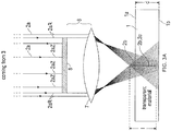
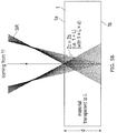
- a method of laser drilling a material includes focusing a pulsed laser beam 2 into a laser beam focal line 2b, oriented along the beam propagation direction.
- laser 3 (not shown) emits laser beam 2, at the beam incidence side of the optical assembly 6 referred to as 2a, which is incident onto the optical assembly 6.
- the optical assembly 6 turns the incident laser beam into an extensive laser beam focal line 2b on the output side over a defined expansion range along the beam direction (length 1 of the focal line).
- the planar substrate 1 to be processed is positioned in the beam path after the optical assembly overlapping at least partially the laser beam focal line 2b of laser beam 2.
- Reference 1a designates the surface of the planar substrate facing the optical assembly 6 or the laser, respectively
- reference 1b designates the reverse surface of substrate 1 usually spaced in parallel.
- the substrate thickness (measured perpendicularly to the planes 1a and 1b, i.e., to the substrate plane) is labeled with d.
- substrate 1 is aligned perpendicularly to the longitudinal beam axis and thus behind the same focal line 2b produced by the optical assembly 6 (the substrate is perpendicular to the drawing plane) and oriented along the beam direction it is positioned relative to the focal line 2b in such a way that the focal line 2b viewed in beam direction starts before the surface 1a of the substrate and stops before the surface 1b of the substrate, i.e. still within the substrate.
- the focal line 2b viewed in beam direction starts before the surface 1a of the substrate and stops before the surface 1b of the substrate, i.e. still within the substrate.
- the extensive laser beam focal line 2b thus generates (in case of a suitable laser intensity along the laser beam focal line 2b which is ensured due to the focusing of laser beam 2 on a section of length 1, i.e. a line focus of length 1) an extensive section 2c viewed along the longitudinal beam direction, along which an induced absorption is generated in the substrate material which induces a defect line or crack formation in the substrate material along section 2c.
- the crack formation is not only local, but over the entire length of the extensive section 2c of the induced absorption.
- the length of section 2c (i.e., after all, the length of the overlapping of laser beam focal line 2b with substrate 1) is labeled with reference L.
- the average diameter or the average extension of the section of the induced absorption (or the sections in the material of substrate 1 undergoing the crack formation) is labeled with reference D.
- This average extension D basically corresponds to the average diameter ⁇ of the laser beam focal line 2b, that is, an average spot diameter in a range of between about 0.1 ⁇ m and about 5 ⁇ m.
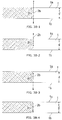
- FIG. 2A shows, substrate material transparent for the wavelength ⁇ of laser beam 2 is heated due to the induced absorption along the focal line 2b.
- FIG. 2B outlines that the warming material will eventually expand so that a correspondingly induced tension leads to micro-crack formation, with the tension being the highest at surface 1a.
- the individual focal lines to be positioned on the substrate surface along parting line 5 should be generated using the optical assembly described below (hereinafter, the optical assembly is alternatively also referred to as laser optics).
- the roughness results particularly from the spot size or the spot diameter of the focal line.
- certain requirements must usually be imposed on the numerical aperture of laser optics 6. These requirements are met by laser optics 6 described below.
- the laser beam must illuminate the optics up to the required aperture, which is typically achieved by means of beam widening using widening telescopes between laser and focusing optics.
- the spot size should not vary too strongly for the purpose of a uniform interaction along the focal line. This can, for example, be ensured (see the embodiment below) by illuminating the focusing optics only in a small, circular area so that the beam opening and thus the percentage of the numerical aperture only vary slightly.
- the laser radiation 2a emitted by laser 3 is first directed onto a circular aperture 8 which is completely opaque for the laser radiation used.
- Aperture 8 is oriented perpendicular to the longitudinal beam axis and is centered on the central beam of the depicted beam bundle 2a.
- the diameter of aperture 8 is selected in such a way that the beam bundles near the center of beam bundle 2a or the central beam (here labeled with 2aZ) hit the aperture and are completely absorbed by it. Only the beams in the outer perimeter range of beam bundle 2a (marginal rays, here labeled with 2aR) are not absorbed due to the reduced aperture size compared to the beam diameter, but pass aperture 8 laterally and hit the marginal areas of the focusing optic elements of the optical assembly 6, which is designed as a spherically cut, bi-convex lens 7 here.
- Lens 7 centered on the central beam is deliberately designed as a non-corrected, bi-convex focusing lens in the form of a common, spherically cut lens. Put another way, the spherical aberration of such a lens is deliberately used.
- aspheres or multi-lens systems deviating from ideally corrected systems, which do not form an ideal focal point but a distinct, elongated focal line of a defined length can also be used (i.e., lenses or systems which do not have a single focal point). The zones of the lens thus focus along a focal line 2b, subject to the distance from the lens center.
- the diameter of aperture 8 across the beam direction is approximately 90% of the diameter of the beam bundle (beam bundle diameter defined by the extension to the decrease to 1/e) and approximately 75% of the diameter of the lens of the optical assembly 6.
- the focal line 2b of a not aberration-corrected spherical lens 7 generated by blocking out the beam bundles in the center is thus used.
- FIG. 3A shows the section in one plane through the central beam, the complete three-dimensional bundle can be seen when the depicted beams are rotated around the focal line 2b.
- This focal line is that the conditions (spot size, laser intensity) along the focal line, and thus along the desired depth in the material, vary and that therefore the desired type of interaction (no melting, induced absorption, thermal-plastic deformation up to crack formation) may possibly only be selected in a part of the focal line. This means in turn that possibly only a part of the incident laser light is absorbed in the desired way. In this way, the efficiency of the process (required average laser power for the desired separation speed) is impaired on the one hand, and on the other hand the laser light might be transmitted into undesired deeper places (parts or layers adherent to the substrate or the substrate holding fixture) and interact there in an undesirable way (heating, diffusion, absorption, unwanted modification).
- FIG. 3B-1-4 show (not only for the optical assembly in FIG. 3A , but basically also for any other applicable optical assembly 6) that the laser beam focal line 2b can be positioned differently by suitably positioning and/or aligning the optical assembly 6 relative to substrate 1 as well as by suitably selecting the parameters of the optical assembly 6:
- the length 1 of the focal line 2b can be adjusted in such a way that it exceeds the substrate thickness d (here by factor 2).
- the laser beam focal line 2b can have a length 1 in a range of between about 0.1 mm and about 100 mm or in a range of between about 0.1 mm and about 10 mm, for example.
- Various embodiments can be configured to have length 1 of about 0.1 mm, 0.2 mm, 0.3 mm, 0.4 mm, 0.5 mm, 0.7 mm, 1 mm, 2 mm, 3 mm or 5 mm, for example. If substrate 1 is placed (viewed in longitudinal beam direction) centrally to focal line 2b, an extensive section of induced absorption 2c is generated over the entire substrate thickness.
- a focal line 2b of length 1 is generated which corresponds more or less to the substrate extension d.
- the length L of the extensive section of induced absorption 2c (which extends here from the substrate surface to a defined substrate depth, but not to the reverse surface 1b) is smaller than the length 1 of focal line 2b.
- FIG. 4 depicts another applicable optical assembly 6.
- the basic construction follows the one described in FIG. 3A so that only the differences are described below.
- the depicted optical assembly is based the use of optics with a non-spherical free surface in order to generate the focal line 2b, which is shaped in such a way that a focal line of defined length 1 is formed.
- aspheres can be used as optic elements of the optical assembly 6.
- a so-called conical prism also often referred to as axicon
- An axicon is a special, conically cut lens which forms a spot source on a line along the optical axis (or transforms a laser beam into a ring).
- the layout of such an axicon is generally known to one of skill in the art; the cone angle in the example is 10°.
- the apex of the axicon labeled here with reference 9 is directed towards the incidence direction and centered on the beam center.
- substrate 1 (here aligned perpendicularly to the main beam axis) can be positioned in the beam path directly behind axicon 9.
- FIG. 4 shows, it is also possible to shift substrate 1 along the beam direction due to the optical characteristics of the axicon without leaving the range of focal line 2b.
- the extensive section of the induced absorption 2c in the material of substrate 1 therefore extends over the entire substrate depth d.
- the depicted layout is subject to the following restrictions: As the focal line of axicon 9 already starts within the lens, a significant part of the laser energy is not focused into part 2c of focal line 2b, which is located within the material, in case of a finite distance between lens and material. Furthermore, length 1 of focal line 2b is related to the beam diameter for the available refraction indices and cone angles of axicon 9, which is why, in case of relatively thin materials (several millimeters), the total focal line is too long, having the effect that the laser energy is again not specifically focused into the material.
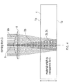
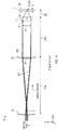
- FIG. 5A depicts such an optical assembly 6 in which a first optical element (viewed along the beam direction) with a non-spherical free surface designed to form an extensive laser beam focal line 2b is positioned in the beam path of laser 3.
- this first optical element is an axicon 10 with a cone angle of 5°, which is positioned perpendicularly to the beam direction and centered on laser beam 3. The apex of the axicon is oriented towards the beam direction.
- a second, focusing optical element here the plano-convex lens 11 (the curvature of which is oriented towards the axicon), is positioned in beam direction at a distance z1 from the axicon 10.
- the distance z1 in this case approximately 300 mm, is selected in such a way that the laser radiation formed by axicon 10 circularly is incident on the marginal area of lens 11.
- Lens 11 focuses the circular radiation on the output side at a distance z2, in this case approximately 20 mm from lens 11, on a focal line 2b of a defined length, in this case 1.5 mm.
- the effective focal length of lens 11 is 25 mm here.
- the circular transformation of the laser beam by axicon 10 is labeled with the reference SR.
- FIG. 5B depicts the formation of the focal line 2b or the induced absorption 2c in the material of substrate 1 according to FIG. 5A in detail.
- the optical characteristics of both elements 10, 11 as well as the positioning of them is selected in such a way that the extension 1 of the focal line 2b in beam direction is exactly identical with the thickness d of substrate 1. Consequently, an exact positioning of substrate 1 along the beam direction is required in order to position the focal line 2b exactly between the two surfaces 1a and 1b of substrate 1, as shown in FIG. 5B .
- the focal line is formed at a certain distance from the laser optics, and if the greater part of the laser radiation is focused up to a desired end of the focal line.
- this can be achieved by illuminating a primarily focusing element 11 (lens) only circularly on a required zone, which, on the one hand, serves to realize the required numerical aperture and thus the required spot size, on the other hand, however, the circle of diffusion diminishes in intensity after the required focal line 2b over a very short distance in the center of the spot, as a basically circular spot is formed. In this way, the crack formation is stopped within a short distance in the required substrate depth.
- a combination of axicon 10 and focusing lens 11 meets this requirement.
- the axicon acts in two different ways: due to the axicon 10, a usually round laser spot is sent to the focusing lens 11 in the form of a ring, and the asphericity of axicon 10 has the effect that a focal line is formed beyond the focal plane of the lens instead of a focal point in the focal plane.
- the length 1 of focal line 2b can be adjusted via the beam diameter on the axicon.
- the numerical aperture along the focal line on the other hand, can be adjusted via the distance z1 axicon-lens and via the cone angle of the axicon. In this way, the entire laser energy can be concentrated in the focal line.
- the circular illumination still has the advantage that, on the one hand, the laser power is used in the best possible way as a large part of the laser light remains concentrated in the required length of the focal line, on the other hand, it is possible to achieve a uniform spot size along the focal line - and thus a uniform separation process along the focal line - due to the circularly illuminated zone in conjunction with the desired aberration set by means of the other optical functions.
- the defect lines 120 extend, for example, through the thickness of the glass sheet, and in the exemplary embodiments described herein are orthogonal to the major (flat) surfaces of the glass sheet.
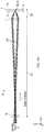
- both effects can be avoided by inserting another lens, a collimating lens 12: this further, positive lens 12 serves to adjust the circular illumination of focusing lens 11 very tightly.
- the focal length f of collimating lens 12 is selected in such a way that the desired circle diameter dr results from distance zla from the axicon to the collimating lens 12, which is equal to f.
- the desired width br of the ring can be adjusted via the distance zlb (collimating lens 12 to focusing lens 11).
- the small width of the circular illumination leads to a short focal line. A minimum can be achieved at distance f.
- the optical assembly 6 depicted in FIG. 6 is thus based on the one depicted in FIG. 5A so that only the differences are described below.
- the collimating lens 12, here also designed as a plano-convex lens (with its curvature towards the beam direction) is additionally placed centrally in the beam path between axicon 10 (with its apex towards the beam direction), on the one side, and the plano-convex lens 11, on the other side.
- the distance of collimating lens 12 from axicon 10 is referred to as zla, the distance of focusing lens 11 from collimating lens 12 as zlb, and the distance of the generated focal line 2b from the focusing lens 11 as z2 (always viewed in beam direction).
- zla the distance of focusing lens 11 from collimating lens 12
- z2 the distance of the generated focal line 2b from the focusing lens 11 as z2 (always viewed in beam direction).
- the circular radiation SR formed by axicon 10 which is incident divergently and under the circle diameter dr on the collimating lens 12, is adjusted to the required circle width br along the distance z1b for an at least approximately constant circle diameter dr at the focusing lens 11.
- a very short focal line 2b is supposed to be generated so that the circle width br of approximately 4 mm at lens 12 is reduced to approximately 0.5 mm at lens 11 due to the focusing properties of lens 12 (circle diameter dr is 22 mm in the example).
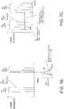
- each "burst" 710 may contain multiple pulses 720 (such as at least 2 pulses, at least 3 pulses as shown in FIGs. 7A-7B , at least 4 pulses, at least 5 pulses as shown in FIG. 7C , at least 10 pulses, at least 15 pulses, at least 20 pulses, or more) of very short duration (e.g., ⁇ 10psec).
- Each pulse 720 within a burst is separated from an adjacent pulse in time by a duration in a range of between about 1 nsec and about 50 nsec, such as approximately 20 nsec (50MHz), with the time often governed by the laser cavity design.
- the time between each "burst" 710 will be much longer, often about 10 ⁇ sec, for a laser burst repetition rate of about 100kHz. That is, a pulse burst is a "pocket" of pulses, and the bursts are separated from one another by a longer duration than the separation of individual adjacent pulses within each burst.
- the exact timings, pulse durations, and burst repetition rates can vary depending on the laser design, but short pulses (i.e., less than about 15 psec) of high intensity have been shown to work well with this technique.
- pulses 720 typically have pulse duration T d of up to 100 psec (for example, 0.1 psec, 5 psec, 10 psec, 15 psec, 18 psec, 20 psec, 22 psec, 25 psec, 30 psec, 50 psec, 75 psec, or therebetween).
- the energy or intensity of each individual pulse 720 within the burst may not be equal to that of other pulses within the burst, and the intensity distribution of the multiple pulses within a burst 710 often follows an exponential decay in time governed by the laser design.
- each pulse 720 within the burst 710 of the exemplary embodiments described herein are separated in time from the subsequent pulse in the burst by a duration T p from 1 nsec to 50 nsec (e.g. 10-50 nsec, or 10-30 nsec, with the time often governed by the laser cavity design).
- T p the time separation between adjacent pulses (pulse -to- pulse separation) within a burst 710 is relatively uniform ( ⁇ 10%).
- each pulse within a burst is separated in time from the subsequent pulse by approximately 20 nsec (50 MHz).
- the pulse to pulse separation T p within a burst is maintained within about ⁇ 10%, or is about ⁇ 2 nsec.
- the time between each "burst" of pulses i.e., time separation T b between bursts
- the time separation T b is around 5 microseconds for a laser with burst repetition rate or frequency of about 200 kHz.
- the laser burst repetition rate is defined as the time between the first pulse in a burst to the first pulse in the subsequent burst.
- the burst repetition frequency may be in a range of between about 1 kHz and about 4 MHz. More preferably, the laser burst repetition rates can be, for example, in a range of between about 10 kHz and 650 kHz.
- the time T b between the first pulse in each burst to the first pulse in the subsequent burst may be 0.25 microsecond (4 MHz burst repetition rate) to 1000 microseconds (1 kHz burst repetition rate), for example 0.5 microseconds (2 MHz burst repetition rate) to 40 microseconds (25 kHz burst repetition rate), or 2 microseconds (500 kHz burst repetition rate) to 20 microseconds (50k Hz burst repetition rate).
- the exact timings, pulse durations, and burst repetition rates can vary depending on the laser design, but short pulses (T d ⁇ 20 psec and preferably T d ⁇ 15 psec) of high intensity have been shown to work particularly well.
- the required energy to modify the material can be described in terms of the burst energy - the energy contained within a burst (each burst 710 contains a series of pulses 720), or in terms of the energy contained within a single laser pulse (many of which may comprise a burst).
- the energy per burst can be from 25-750 ⁇ J, more preferably 50-500 ⁇ J, or 50-250 ⁇ J. In some embodiments the energy per burst is 100-250 ⁇ J.
- the energy of an individual pulse within the pulse burst will be less, and the exact individual laser pulse energy will depend on the number of pulses 720 within the pulse burst 710 and the rate of decay (e.g., exponential decay rate) of the laser pulses with time as shown in FIGs. 7B and 7C .
- the rate of decay e.g., exponential decay rate
- each individual laser pulse 720 will contain less energy than if the same pulse burst 710 had only 2 individual laser pulses.
- the use of laser capable of generating such pulse bursts is advantageous for cutting or modifying transparent materials, for example glass.
- the use of a pulse burst sequence that spreads the laser energy over a rapid sequence of pulses within the burst 710 allows access to larger timescales of high intensity interaction with the material than is possible with single-pulse lasers.
- a single-pulse can be expanded in time, as this is done the intensity within the pulse must drop as roughly one over the pulse width. Hence if a 10 psec single pulse is expanded to a 10 nsec pulse, the intensity drops by roughly three orders of magnitude.
- the intensity during each pulse 720 within the burst 710 can remain very high - for example three 10 psec pulses 720 spaced apart in time by approximately 10 nsec still allows the intensity within each pulse to be approximately three times higher than that of a single 10 psec pulse, while the laser is allowed to interact with the material over a timescale that is now three orders of magnitude larger.
- This adjustment of multiple pulses 720 within a burst thus allows manipulation of time-scale of the laser-material interaction in ways that can facilitate greater or lesser light interaction with a pre-existing plasma plume, greater or lesser light-material interaction with atoms and molecules that have been pre-excited by an initial or previous laser pulse, and greater or lesser heating effects within the material that can promote the controlled growth of microcracks.
- the required amount of burst energy to modify the material will depend on the substrate material composition and the length of the line focus used to interact with the substrate. The longer the interaction region, the more the energy is spread out, and higher burst energy will be required.
- the exact timings, pulse durations, and burst repetition rates can vary depending on the laser design, but short pulses ( ⁇ 15 psec, or ⁇ 10 psec) of high intensity have been shown to work well with this technique.
- the defect line or a hole is formed in the material when a single burst of laser pulses strikes essentially the same location on the glass. That is, multiple laser pulses within a single burst correspond to a single defect line or a hole location in the glass.
- the glass is translated (for example by a constantly moving stage) (or the beam is moved relative to the glass, the individual pulses within the burst cannot be at exactly the same spatial location on the glass.
- the laser beam has a wavelength less than or equal to about 850 nm, the wavelength selected such that the material is substantially transparent (i.e., absorption less than about 10%, preferably less than about 1% per mm of material depth) at this wavelength, the laser beam having an average laser energy measured at the material greater than about 50 ⁇ J per mm of material thickness, and pulses having a duration in a range of between greater than about 1 picosecond and less than about 100 picoseconds, and a pulse burst repetition rate in a range of between about 1 kHz and about 2 MHz.
- the method then includes directing the laser beam focal line into the material, the laser beam focal line generating an induced absorption within the material, the induced absorption producing a defect line along the laser beam focal line within the material, and producing subsurface damage up to a depth less than or equal to 100 ⁇ m within the material, for example than or equal to about 75 ⁇ m within the material, and in some embodiments ⁇ 50 ⁇ m, for example, ⁇ 40 ⁇ m.
- the depth of subsurface damage can be measured by using a confocal microscope to look at the cut surface, the microscope having an optical resolution of a few nm. Surface reflections are ignored while cracks are sought out down into the material, the cracks showing up as bright lines. One then steps into the material until there are no more "sparks", collecting images at regular intervals. The images are then manually processed by looking for cracks and tracing them through the depth of the glass to get a maximum depth (typically measured in microns ( ⁇ m)) of subsurface damage. There are typically thousands and thousands of cracks, so one typically just tracks the largest ones. One typically repeats this process on about 5 locations of a cut edge. Any cracks that are directly perpendicular to the edge of the glass will not be detected by this method.
- the method further includes translating the material and the laser beam relative to each other, thereby drilling a plurality of defect lines within the material, the defect lines spaced apart so as to separate the material into at least two pieces.
- the laser triggering generally is synchronized with the stage driven motion of the material beneath the beam, so laser pulse bursts are triggered at a fixed interval, such as for example every 1 ⁇ m, or every 5 ⁇ m.
- the exact spacing between adjacent perforations or defect lines is determined by the material properties that facilitate crack propagation from perforated hole (i.e., defect line) to perforated hole, given the stress level in the substrate.
- interposers in contrast to cutting a substrate, it is also possible to use the same method to only perforate the material, such as for creating holes for conducting electrical signals from one part to another, thereby creating components called interposers.
- the defect lines are generally separated by much greater distance than required for cutting - instead of a pitch of about 10 ⁇ m or less, the spacing between defect lines can be hundreds of microns.
- the exact locations of the defect lines need not be at regular intervals - the location simply is determined by when the laser is triggered to fire, and may be at any location within the part.
- the embodiments of the process described herein can cut glass at a cutting speed of 0.25 m/sec, or faster.
- a cut speed is the rate the laser beam moves relative to the surface of the transparent material (e.g., glass) while creating multiple holes or modified regions.)
- High cut speeds such as, for example 400 mm/sec, 500 mm/sec, 750 mm/sec, 1 m/sec, 1.2 m/sec, 1.5 m/sec, or 2 m/sec, or even 3 m/sec to 4 m/sec are often desired in order to minimize capital investment for manufacturing, and to optimize equipment utilization rate.
- the laser power is equal to the burst energy multiplied by the burst repetition frequency (rate) of the laser.
- the damage tracks are typically spaced apart by 1-25 microns, in some embodiments the spacing is preferably 2 microns or larger- for example 2-12 microns, or for example 3-10 microns.
- 3 micron hole pitch corresponds to a pulse burst laser with at least 100 kHz burst repetition rate.
- a 3 micron pitch corresponds to a burst-pulsed laser with at least 200kHz burst repetition rate.
- a pulse burst laser that produces at least 40 ⁇ J/burst at 200kHz, and cuts at a 600 mm/s cutting speed needs to have laser power of at least 8 Watts. Higher cut speeds therefore require even higher laser powers.
- the laser power of the pulse burst picosecond laser is 6 watts or higher, more preferably at least 8 Watts or higher, and even more preferably at least 10W or higher.
- Too long a pitch may result in "uncontrolled microcracking" - i.e., where instead of propagating from hole to hole the microcracks propagate along a different path, and cause the glass to crack in a different (undesirable) direction. This may ultimately lower the strength of the separated glass part, since the residual microcracks will acts as flaws which weaken the glass.
- Too high a burst energy (e.g., >2500 ⁇ J/burst, and in some embodiments >500 ⁇ J/burst) used to form each damage track can cause "healing" or re-melting of already formed microcracks of adjacent damage tracks, which will inhibit separation of the glass. Accordingly, it is preferred that burst energy be ⁇ 2500 ⁇ J/burst, for example, ⁇ 500 ⁇ J/burst. Also, using a burst energy that is too high can cause formation of microcracks that are extremely large and create flaws which reduce the edge strength of the parts after separation. Too low a burst energy ( ⁇ 40 ⁇ J/burst) may result in no appreciable damage track formed within the glass, and hence very high separation strength or complete inability to separate along the perforated contour.
- a burst energy e.g., >2500 ⁇ J/burst, and in some embodiments >500 ⁇ J/burst
- Typical exemplary cutting rates (speeds) enabled by this process are, for example, 0.250 m/sec and higher.
- the cutting rates are at least 300 mm/sec.
- the cutting rates are at least 400 mm/sec, for example 500 mm/sec to 2000 mm/sec, or higher.
- the picosecond laser utilizes pulse bursts to produce defect lines with periodicity between 0.5 microns and 13 microns, e.g. 0.5 and 3 microns.
- the pulsed laser has laser power of 10 W-100 W and the material and/or the laser beam are translated relative to one another at a rate of at least 0.25 m/sec, for example at the rate of 0.25 to 0.35 m/sec, or 0.4 m/sec to 5 m/sec.
- each pulse burst of the pulsed laser beam has an average laser energy measured at the workpiece greater than 40 microJoules per burst mm thickness of workpiece.
- each pulse burst of the pulsed laser beam has an average laser energy measured at the workpiece greater of less than 2500 microJoules per burst per mm thickness of workpiece, and preferably less than about 2000 microJoules per burst per mm, and in some embodiments less than 1500 microJoules per burst per mm thickness of workpiece, for example not more than 500 microJoules per burst per mm thickness of workpiece
- the laser produces pulse bursts with at least 2 pulses per burst.
- the pulsed laser has laser power of 10W-150W (e.g., 10-100W) and produces pulse bursts with at least 2 pulses per burst (e.g., 2 to 25 pulses per burst).
- the pulsed laser has the power of 25 W to 60 W, and produces pulse bursts with at least 2 to 25 pulses per burst, and the distance or periodicity between the adjacent defect lines produced by the laser bursts is 2-10 microns.
- the pulsed laser has laser power of 10W to 100W, produces pulse bursts with at least 2 pulses per burst, and the workpiece and the laser beam are translated relative to one another at a rate of at least 0.25 m/sec. In some embodiments the workpiece and/or the laser beam are translated relative to one another at a rate of at least 0.4 m/sec
- laser powers should preferably be 10 W-150W, with burst energy of 40-750 ⁇ J/burst, 2-25 bursts per pulse (depending on the material that is cut), and hole separation (or pitch) of 3 to 15 ⁇ m, or 3-10 ⁇ m.
- the use of picosecond pulse burst lasers would be preferable for these cutting speeds because they generate high power and the required number of pulses per burst.
- the pulsed laser produces 10-100W of power, for example 25 W to 60 Watts, and produces pulse bursts at least 2-25 pulses per burst and the distance between the defect lines is 2-15 microns; and the laser beam and/or the workpiece are translated relative to one another at a rate of at least 0.25 m/sec, in some embodiments at least 0.4 m/sec, for example 0.5 m/sec to 5 m/sec, or faster.
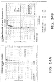
- the edge strength of samples cut using the 532 nm process described above is shown in FIG. 9 .
- Tables 1 and 2 below samples cut using the 532 nm process had an average subsurface damage of about 23 ⁇ m, while samples cut using a 1064 nm process described in U.S. Application No. 61/752,489 filed on January 15, 2013 had an average subsurface damage of about 74 ⁇ m. Table 1.
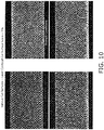
- FIG. 10 includes several SEM micrographs of several cut surfaces, showing laser confocal cut surface scans at 20x magnification.
- Table 3 shows measurements of surface roughness as a function of pulse spacing, measured with a Zygo optical surface profiler, showing that Ra and RMS surface roughness both appear to increase with pulse spacing.
- Table 3. Zygo Surface Roughness vs. Pulse Spacing Sample ID Pulse Spacing Varied Ra ( ⁇ m) AVG 5 Points RMS ( ⁇ m) AVG 5 Points 1 .31 .4 2 .43 .56 3 .54 .7 4 .66 .83
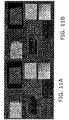
- FIGS. 11A-11D Zygo representative scans are shown in FIGS. 11A-11D .
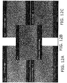
- FIGS. 12A-12C show photographs of edges of samples cut using the 532 nm process ( FIGS. 12A and 12C ) and a reference edge of a sample cut using the 1064 nm process.
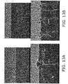
- FIG. 13A shows a higher magnification photograph of features made with the 1064 nm process, where the diameter of the hole was measured at 347 nm, as compared to the diameter of a hole made with the 532 nm process ( FIG. 13B ) that was 190 nm.
- Table 4 shows a comparison of the RMS surface roughness and subsurface damage (SSD) between samples cut using the 1064 nm process and samples cut using the 532 nm described above.
- Table 4. 1064 nm v. 532 nm Direct Comparison 1064nm RMS (nm) 1 532 nm RMS (nm) 2 1064 nm SSD ( ⁇ m) 1 532nm SSD( ⁇ m) 2 Avg 1120.8 556 74.4 23 Range 226 20 12 8 Std Dev 91.3 9 5.5 3 Notes: 1) 0.55 mm 2320 FG glass 2) 0.40 mm 2320 FG glass (2 ⁇ m spacing cut - strength sample)
- FIGS. 14A and 14B show a comparison of edge strength of samples cut using the 1064 nm process ( FIG. 14A ) and the 532 nm process ( FIG. 14B ), showing that the edge strengths of the samples produced by the two processes are relatively similar.
Applications Claiming Priority (4)
| Application Number | Priority Date | Filing Date | Title |
|---|---|---|---|
| US201361917140P | 2013-12-17 | 2013-12-17 | |
| US201462022888P | 2014-07-10 | 2014-07-10 | |
| US14/529,801 US9687936B2 (en) | 2013-12-17 | 2014-10-31 | Transparent material cutting with ultrafast laser and beam optics |
| PCT/US2014/070275 WO2015095014A1 (en) | 2013-12-17 | 2014-12-15 | Transparent material cutting with ultrafast laser and beam optics |
Publications (2)
| Publication Number | Publication Date |
|---|---|
| EP3083126A1 EP3083126A1 (en) | 2016-10-26 |
| EP3083126B1 true EP3083126B1 (en) | 2020-02-26 |
Family
ID=53367591
Family Applications (1)
| Application Number | Title | Priority Date | Filing Date |
|---|---|---|---|
| EP14822005.6A Active EP3083126B1 (en) | 2013-12-17 | 2014-12-15 | Transparent material cutting with ultrafast laser and beam optics |
Country Status (8)
| Country | Link |
|---|---|
| US (2) | US9687936B2 (ja) |
| EP (1) | EP3083126B1 (ja) |
| JP (1) | JP6571085B2 (ja) |
| CN (1) | CN106170367A (ja) |
| MX (1) | MX364462B (ja) |
| RU (1) | RU2673258C1 (ja) |
| TW (1) | TWI645929B (ja) |
| WO (1) | WO2015095014A1 (ja) |
Families Citing this family (54)
| Publication number | Priority date | Publication date | Assignee | Title |
|---|---|---|---|---|
| WO2014079478A1 (en) | 2012-11-20 | 2014-05-30 | Light In Light Srl | High speed laser processing of transparent materials |
| EP2754524B1 (de) * | 2013-01-15 | 2015-11-25 | Corning Laser Technologies GmbH | Verfahren und Vorrichtung zum laserbasierten Bearbeiten von flächigen Substraten, d.h. Wafer oder Glaselement, unter Verwendung einer Laserstrahlbrennlinie |
| EP2781296B1 (de) | 2013-03-21 | 2020-10-21 | Corning Laser Technologies GmbH | Vorrichtung und verfahren zum ausschneiden von konturen aus flächigen substraten mittels laser |
| US20150059411A1 (en) * | 2013-08-29 | 2015-03-05 | Corning Incorporated | Method of separating a glass sheet from a carrier |
| US9676167B2 (en) | 2013-12-17 | 2017-06-13 | Corning Incorporated | Laser processing of sapphire substrate and related applications |
| US9517963B2 (en) | 2013-12-17 | 2016-12-13 | Corning Incorporated | Method for rapid laser drilling of holes in glass and products made therefrom |
| US20150166393A1 (en) * | 2013-12-17 | 2015-06-18 | Corning Incorporated | Laser cutting of ion-exchangeable glass substrates |
| US9701563B2 (en) | 2013-12-17 | 2017-07-11 | Corning Incorporated | Laser cut composite glass article and method of cutting |
| US10442719B2 (en) | 2013-12-17 | 2019-10-15 | Corning Incorporated | Edge chamfering methods |
| US9850160B2 (en) | 2013-12-17 | 2017-12-26 | Corning Incorporated | Laser cutting of display glass compositions |
| US20150165560A1 (en) | 2013-12-17 | 2015-06-18 | Corning Incorporated | Laser processing of slots and holes |
| US9815730B2 (en) | 2013-12-17 | 2017-11-14 | Corning Incorporated | Processing 3D shaped transparent brittle substrate |
| US11556039B2 (en) | 2013-12-17 | 2023-01-17 | Corning Incorporated | Electrochromic coated glass articles and methods for laser processing the same |
| US9815144B2 (en) | 2014-07-08 | 2017-11-14 | Corning Incorporated | Methods and apparatuses for laser processing materials |
| CN107073642B (zh) * | 2014-07-14 | 2020-07-28 | 康宁股份有限公司 | 使用长度和直径可调的激光束焦线来加工透明材料的系统和方法 |
| US10611667B2 (en) | 2014-07-14 | 2020-04-07 | Corning Incorporated | Method and system for forming perforations |
| CN107073641B (zh) | 2014-07-14 | 2020-11-10 | 康宁股份有限公司 | 接口块;用于使用这种接口块切割在波长范围内透明的衬底的系统和方法 |
| EP3536440A1 (en) | 2014-07-14 | 2019-09-11 | Corning Incorporated | Glass article with a defect pattern |
| US10047001B2 (en) | 2014-12-04 | 2018-08-14 | Corning Incorporated | Glass cutting systems and methods using non-diffracting laser beams |
| EP3245166B1 (en) | 2015-01-12 | 2020-05-27 | Corning Incorporated | Laser cutting of thermally tempered substrates using the multi photon absorption method |
| WO2016138054A1 (en) | 2015-02-27 | 2016-09-01 | Corning Incorporated | Optical assembly having microlouvers |
| HUE055461T2 (hu) | 2015-03-24 | 2021-11-29 | Corning Inc | Kijelzõ üveg kompozíciók lézeres vágása és feldolgozása |
| CN107666983B (zh) | 2015-03-27 | 2020-10-02 | 康宁股份有限公司 | 可透气窗及其制造方法 |
| WO2016183148A1 (en) | 2015-05-13 | 2016-11-17 | Corning Incorporated | Light guides with reduced hot spots and methods for making the same |
| WO2017011296A1 (en) * | 2015-07-10 | 2017-01-19 | Corning Incorporated | Methods of continuous fabrication of holes in flexible substrate sheets and products relating to the same |
| DE102015111490A1 (de) * | 2015-07-15 | 2017-01-19 | Schott Ag | Verfahren und Vorrichtung zum lasergestützten Abtrennen eines Teilstücks von einem flächigen Glaselement |
| EP3338520A1 (en) * | 2015-08-21 | 2018-06-27 | Corning Incorporated | Glass substrate assemblies having low dielectric properties |
| US10442720B2 (en) * | 2015-10-01 | 2019-10-15 | AGC Inc. | Method of forming hole in glass substrate by using pulsed laser, and method of producing glass substrate provided with hole |
| SG11201809797PA (en) | 2016-05-06 | 2018-12-28 | Corning Inc | Laser cutting and removal of contoured shapes from transparent substrates |
| US10410883B2 (en) | 2016-06-01 | 2019-09-10 | Corning Incorporated | Articles and methods of forming vias in substrates |
| US10794679B2 (en) | 2016-06-29 | 2020-10-06 | Corning Incorporated | Method and system for measuring geometric parameters of through holes |
| WO2018022476A1 (en) | 2016-07-29 | 2018-02-01 | Corning Incorporated | Apparatuses and methods for laser processing |
| US10522963B2 (en) | 2016-08-30 | 2019-12-31 | Corning Incorporated | Laser cutting of materials with intensity mapping optical system |
| KR102078294B1 (ko) | 2016-09-30 | 2020-02-17 | 코닝 인코포레이티드 | 비-축대칭 빔 스폿을 이용하여 투명 워크피스를 레이저 가공하기 위한 기기 및 방법 |
| KR102428350B1 (ko) * | 2016-10-24 | 2022-08-02 | 코닝 인코포레이티드 | 시트형 유리 기판의 레이저 기반 기계 가공을 위한 기판 프로세싱 스테이션 |
| US10752534B2 (en) | 2016-11-01 | 2020-08-25 | Corning Incorporated | Apparatuses and methods for laser processing laminate workpiece stacks |
| US10688599B2 (en) | 2017-02-09 | 2020-06-23 | Corning Incorporated | Apparatus and methods for laser processing transparent workpieces using phase shifted focal lines |
| WO2018189296A1 (en) | 2017-04-12 | 2018-10-18 | Saint-Gobain Glass France | Electrochromic structure and method of separating electrochromic structure |
| DE102017208290A1 (de) * | 2017-05-17 | 2018-11-22 | Schott Ag | Vorrichtung und Verfahren zum Bearbeiten eines Werkstücks entlang einer vorbestimmten Bearbeitungslinie |
| US11078112B2 (en) | 2017-05-25 | 2021-08-03 | Corning Incorporated | Silica-containing substrates with vias having an axially variable sidewall taper and methods for forming the same |
| US10580725B2 (en) | 2017-05-25 | 2020-03-03 | Corning Incorporated | Articles having vias with geometry attributes and methods for fabricating the same |
| US10626040B2 (en) | 2017-06-15 | 2020-04-21 | Corning Incorporated | Articles capable of individual singulation |
| US10947148B2 (en) | 2017-08-07 | 2021-03-16 | Seagate Technology Llc | Laser beam cutting/shaping a glass substrate |
| US10906832B2 (en) * | 2017-08-11 | 2021-02-02 | Corning Incorporated | Apparatuses and methods for synchronous multi-laser processing of transparent workpieces |
| US10689286B2 (en) | 2017-10-13 | 2020-06-23 | Seagate Technology Llc | Separation of glass shapes using engineered induced thermal gradients after process cutting |
| US11554984B2 (en) | 2018-02-22 | 2023-01-17 | Corning Incorporated | Alkali-free borosilicate glasses with low post-HF etch roughness |
| TWI677395B (zh) * | 2018-03-31 | 2019-11-21 | 財團法人工業技術研究院 | 硬脆材料切割方法及其裝置 |
| US10615044B1 (en) * | 2018-10-18 | 2020-04-07 | Asm Technology Singapore Pte Ltd | Material cutting using laser pulses |
| CN110039205B (zh) * | 2019-04-30 | 2021-07-20 | 大族激光科技产业集团股份有限公司 | Led晶圆片的加工方法 |
| EP3770698A1 (fr) | 2019-07-26 | 2021-01-27 | Comadur S.A. | Pierre minérale de type monocristalline munie d'un cone de recentrage d'un pivot, et son procédé de fabrication |
| RU2720791C1 (ru) * | 2019-09-06 | 2020-05-13 | Общество с ограниченной ответственностью "НАУЧНО-ТЕХНИЧЕСКОЕ ОБЪЕДИНЕНИЕ "ИРЭ-Полюс" (ООО НТО "ИРЭ-Полюс") | Способ лазерной обработки прозрачного хрупкого материала и устройство его реализующее |
| CN110711937B (zh) * | 2019-11-14 | 2022-01-04 | 安徽同兴科技发展有限责任公司 | 一种切割机激光对焦的参数确定方法 |
| CN114178710A (zh) * | 2020-08-24 | 2022-03-15 | 奥特斯(中国)有限公司 | 部件承载件及其制造方法 |
| CN112372151A (zh) * | 2020-10-29 | 2021-02-19 | 大昶(重庆)电子科技有限公司 | 一种玻璃用镭切设备及其生产工艺 |
Family Cites Families (91)
| Publication number | Priority date | Publication date | Assignee | Title |
|---|---|---|---|---|
| US1790397A (en) | 1931-01-27 | Glass workins machine | ||
| US3647410A (en) | 1969-09-09 | 1972-03-07 | Owens Illinois Inc | Glass ribbon machine blow head mechanism |
| US3775084A (en) | 1970-01-02 | 1973-11-27 | Owens Illinois Inc | Pressurizer apparatus for glass ribbon machine |
| US4646308A (en) | 1985-09-30 | 1987-02-24 | Spectra-Physics, Inc. | Synchronously pumped dye laser using ultrashort pump pulses |
| US4918751A (en) | 1987-10-05 | 1990-04-17 | The University Of Rochester | Method for optical pulse transmission through optical fibers which increases the pulse power handling capacity of the fibers |
| US4764930A (en) | 1988-01-27 | 1988-08-16 | Intelligent Surgical Lasers | Multiwavelength laser source |
| US4907586A (en) | 1988-03-31 | 1990-03-13 | Intelligent Surgical Lasers | Method for reshaping the eye |
| US5040182A (en) | 1990-04-24 | 1991-08-13 | Coherent, Inc. | Mode-locked laser |
| JPH07503382A (ja) | 1991-11-06 | 1995-04-13 | ライ,シュイ,ティー. | 角膜手術装置及び方法 |
| US5265107A (en) | 1992-02-05 | 1993-11-23 | Bell Communications Research, Inc. | Broadband absorber having multiple quantum wells of different thicknesses |
| CA2112843A1 (en) | 1993-02-04 | 1994-08-05 | Richard C. Ujazdowski | Variable repetition rate picosecond laser |
| JPH06318756A (ja) | 1993-05-06 | 1994-11-15 | Toshiba Corp | レ−ザ装置 |
| US5637244A (en) * | 1993-05-13 | 1997-06-10 | Podarok International, Inc. | Method and apparatus for creating an image by a pulsed laser beam inside a transparent material |
| US6489589B1 (en) | 1994-02-07 | 2002-12-03 | Board Of Regents, University Of Nebraska-Lincoln | Femtosecond laser utilization methods and apparatus and method for producing nanoparticles |
| US5436925A (en) | 1994-03-01 | 1995-07-25 | Hewlett-Packard Company | Colliding pulse mode-locked fiber ring laser using a semiconductor saturable absorber |
| US5400350A (en) | 1994-03-31 | 1995-03-21 | Imra America, Inc. | Method and apparatus for generating high energy ultrashort pulses |
| US5778016A (en) | 1994-04-01 | 1998-07-07 | Imra America, Inc. | Scanning temporal ultrafast delay methods and apparatuses therefor |
| JP2526806B2 (ja) | 1994-04-26 | 1996-08-21 | 日本電気株式会社 | 半導体レ―ザおよびその動作方法 |
| WO1995031023A1 (en) | 1994-05-09 | 1995-11-16 | Massachusetts Institute Of Technology | Dispersion-compensated laser using prismatic end elements |
| US6016324A (en) | 1994-08-24 | 2000-01-18 | Jmar Research, Inc. | Short pulse laser system |
| US5776220A (en) | 1994-09-19 | 1998-07-07 | Corning Incorporated | Method and apparatus for breaking brittle materials |
| US5696782A (en) | 1995-05-19 | 1997-12-09 | Imra America, Inc. | High power fiber chirped pulse amplification systems based on cladding pumped rare-earth doped fibers |
| JPH09207343A (ja) * | 1995-11-29 | 1997-08-12 | Matsushita Electric Ind Co Ltd | レーザ加工方法 |
| US5736709A (en) | 1996-08-12 | 1998-04-07 | Armco Inc. | Descaling metal with a laser having a very short pulse width and high average power |
| US7353829B1 (en) | 1996-10-30 | 2008-04-08 | Provectus Devicetech, Inc. | Methods and apparatus for multi-photon photo-activation of therapeutic agents |
| US6156030A (en) | 1997-06-04 | 2000-12-05 | Y-Beam Technologies, Inc. | Method and apparatus for high precision variable rate material removal and modification |
| BE1011208A4 (fr) | 1997-06-11 | 1999-06-01 | Cuvelier Georges | Procede de decalottage de pieces en verre. |
| DE19728766C1 (de) | 1997-07-07 | 1998-12-17 | Schott Rohrglas Gmbh | Verwendung eines Verfahrens zur Herstellung einer Sollbruchstelle bei einem Glaskörper |
| US6078599A (en) | 1997-07-22 | 2000-06-20 | Cymer, Inc. | Wavelength shift correction technique for a laser |
| DE19750320C1 (de) | 1997-11-13 | 1999-04-01 | Max Planck Gesellschaft | Verfahren und Vorrichtung zur Lichtpulsverstärkung |
| GB2335603B (en) | 1997-12-05 | 2002-12-04 | Thermolase Corp | Skin enhancement using laser light |
| US6501578B1 (en) | 1997-12-19 | 2002-12-31 | Electric Power Research Institute, Inc. | Apparatus and method for line of sight laser communications |
| JPH11197498A (ja) | 1998-01-13 | 1999-07-27 | Japan Science & Technology Corp | 無機材料内部の選択的改質方法及び内部が選択的に改質された無機材料 |
| US6272156B1 (en) | 1998-01-28 | 2001-08-07 | Coherent, Inc. | Apparatus for ultrashort pulse transportation and delivery |
| JPH11269683A (ja) | 1998-03-18 | 1999-10-05 | Armco Inc | 金属表面から酸化物を除去する方法及び装置 |
| US6160835A (en) | 1998-03-20 | 2000-12-12 | Rocky Mountain Instrument Co. | Hand-held marker with dual output laser |
| US6256328B1 (en) | 1998-05-15 | 2001-07-03 | University Of Central Florida | Multiwavelength modelocked semiconductor diode laser |
| JPH11347758A (ja) | 1998-06-10 | 1999-12-21 | Mitsubishi Heavy Ind Ltd | 超精密加工装置 |
| JP4396953B2 (ja) | 1998-08-26 | 2010-01-13 | 三星電子株式会社 | レーザ切断装置および切断方法 |
| EA199900040A1 (ru) * | 1998-10-13 | 1999-10-28 | Ооо "Лазтекс" | Способ резки пластин хрупких материалов |
| US7649153B2 (en) * | 1998-12-11 | 2010-01-19 | International Business Machines Corporation | Method for minimizing sample damage during the ablation of material using a focused ultrashort pulsed laser beam |
| US6445491B2 (en) | 1999-01-29 | 2002-09-03 | Irma America, Inc. | Method and apparatus for optical sectioning and imaging using time-gated parametric image amplification |
| US6381391B1 (en) | 1999-02-19 | 2002-04-30 | The Regents Of The University Of Michigan | Method and system for generating a broadband spectral continuum and continuous wave-generating system utilizing same |
| US6484052B1 (en) | 1999-03-30 | 2002-11-19 | The Regents Of The University Of California | Optically generated ultrasound for enhanced drug delivery |
| US6373565B1 (en) | 1999-05-27 | 2002-04-16 | Spectra Physics Lasers, Inc. | Method and apparatus to detect a flaw in a surface of an article |
| US6449301B1 (en) | 1999-06-22 | 2002-09-10 | The Regents Of The University Of California | Method and apparatus for mode locking of external cavity semiconductor lasers with saturable Bragg reflectors |
| US6573026B1 (en) | 1999-07-29 | 2003-06-03 | Corning Incorporated | Femtosecond laser writing of glass, including borosilicate, sulfide, and lead glasses |
| US6339208B1 (en) | 2000-01-19 | 2002-01-15 | General Electric Company | Method of forming cooling holes |
| US6552301B2 (en) | 2000-01-25 | 2003-04-22 | Peter R. Herman | Burst-ultrafast laser machining method |
| JP4659300B2 (ja) | 2000-09-13 | 2011-03-30 | 浜松ホトニクス株式会社 | レーザ加工方法及び半導体チップの製造方法 |
| KR100673073B1 (ko) | 2000-10-21 | 2007-01-22 | 삼성전자주식회사 | 레이저 빔을 이용한 비금속 기판의 절단 방법 및 장치 |
| SG108262A1 (en) | 2001-07-06 | 2005-01-28 | Inst Data Storage | Method and apparatus for cutting a multi-layer substrate by dual laser irradiation |
| US6552298B1 (en) * | 2001-09-28 | 2003-04-22 | Corning Incorporated | Apparatus and method for making a lens on the end of an optical waveguide fiber |
| FR2855084A1 (fr) | 2003-05-22 | 2004-11-26 | Air Liquide | Optique de focalisation pour le coupage laser |
| JP2005138143A (ja) | 2003-11-06 | 2005-06-02 | Disco Abrasive Syst Ltd | レーザ光線を利用する加工装置 |
| JP4418282B2 (ja) | 2004-03-31 | 2010-02-17 | 株式会社レーザーシステム | レーザ加工方法 |
| US7804043B2 (en) | 2004-06-15 | 2010-09-28 | Laserfacturing Inc. | Method and apparatus for dicing of thin and ultra thin semiconductor wafer using ultrafast pulse laser |
| JP4692717B2 (ja) | 2004-11-02 | 2011-06-01 | 澁谷工業株式会社 | 脆性材料の割断装置 |
| JP4222296B2 (ja) | 2004-11-22 | 2009-02-12 | 住友電気工業株式会社 | レーザ加工方法とレーザ加工装置 |
| JP4490883B2 (ja) | 2005-07-19 | 2010-06-30 | 株式会社レーザーシステム | レーザ加工装置およびレーザ加工方法 |
| RU2288196C1 (ru) * | 2005-08-26 | 2006-11-27 | Борис Григорьевич Бердитчевский | Способ создания цветных изображений в прозрачных стеклах |
| US9138913B2 (en) * | 2005-09-08 | 2015-09-22 | Imra America, Inc. | Transparent material processing with an ultrashort pulse laser |
| US7626138B2 (en) | 2005-09-08 | 2009-12-01 | Imra America, Inc. | Transparent material processing with an ultrashort pulse laser |
| ES2428826T3 (es) | 2006-07-03 | 2013-11-11 | Hamamatsu Photonics K.K. | Procedimiento de procesamiento por láser y chip |
| US8168514B2 (en) | 2006-08-24 | 2012-05-01 | Corning Incorporated | Laser separation of thin laminated glass substrates for flexible display applications |
| DE102007024700A1 (de) * | 2007-05-25 | 2008-12-04 | Fraunhofer-Gesellschaft zur Förderung der angewandten Forschung e.V. | Verfahren zur Materialbearbeitung mit Laserstrahlung sowie Vorrichtung zur Durchführung des Verfahrens |
| JP5345334B2 (ja) | 2008-04-08 | 2013-11-20 | 株式会社レミ | 脆性材料の熱応力割断方法 |
| JP5071868B2 (ja) * | 2008-08-11 | 2012-11-14 | オムロン株式会社 | レーザ加工方法、レーザ加工装置、光学素子の製造方法、および光学素子 |
| US20100252959A1 (en) | 2009-03-27 | 2010-10-07 | Electro Scientific Industries, Inc. | Method for improved brittle materials processing |
| KR101561729B1 (ko) | 2009-05-06 | 2015-10-19 | 코닝 인코포레이티드 | 유리 기판의 캐리어 |
| JP2013503105A (ja) | 2009-08-28 | 2013-01-31 | コーニング インコーポレイテッド | 化学強化ガラス基板からガラス品をレーザ割断するための方法 |
| US20120234807A1 (en) | 2009-12-07 | 2012-09-20 | J.P. Sercel Associates Inc. | Laser scribing with extended depth affectation into a workplace |
| AU2011279374A1 (en) * | 2010-07-12 | 2013-02-07 | Filaser Usa Llc | Method of material processing by laser filamentation |
| WO2012070490A1 (ja) * | 2010-11-24 | 2012-05-31 | 株式会社フジクラ | 微細孔の製造方法および微細孔を有する基体 |
| RU2459691C2 (ru) * | 2010-11-29 | 2012-08-27 | Юрий Георгиевич Шретер | Способ отделения поверхностного слоя полупроводникового кристалла (варианты) |
| US8539794B2 (en) | 2011-02-01 | 2013-09-24 | Corning Incorporated | Strengthened glass substrate sheets and methods for fabricating glass panels from glass substrate sheets |
| US8933367B2 (en) | 2011-02-09 | 2015-01-13 | Sumitomo Electric Industries, Ltd. | Laser processing method |
| CN103380482B (zh) | 2011-02-10 | 2016-05-25 | 信越聚合物株式会社 | 单结晶基板制造方法及内部改质层形成单结晶部件 |
| DE102011000768B4 (de) | 2011-02-16 | 2016-08-18 | Ewag Ag | Laserbearbeitungsverfahren und Laserbearbeitungsvorrichtung mit umschaltbarer Laseranordnung |
| KR101120471B1 (ko) | 2011-08-05 | 2012-03-05 | (주)지엘코어 | 다중 초점 방식의 펄스 레이저를 이용한 취성 재료 절단 장치 |
| US10239160B2 (en) | 2011-09-21 | 2019-03-26 | Coherent, Inc. | Systems and processes that singulate materials |
| TW201343296A (zh) | 2012-03-16 | 2013-11-01 | Ipg Microsystems Llc | 使一工件中具有延伸深度虛飾之雷射切割系統及方法 |
| FR2989294B1 (fr) | 2012-04-13 | 2022-10-14 | Centre Nat Rech Scient | Dispositif et methode de nano-usinage par laser |
| CN102672355B (zh) | 2012-05-18 | 2015-05-13 | 杭州士兰明芯科技有限公司 | Led衬底的划片方法 |
| US9938180B2 (en) | 2012-06-05 | 2018-04-10 | Corning Incorporated | Methods of cutting glass using a laser |
| WO2014079478A1 (en) | 2012-11-20 | 2014-05-30 | Light In Light Srl | High speed laser processing of transparent materials |
| EP2754524B1 (de) | 2013-01-15 | 2015-11-25 | Corning Laser Technologies GmbH | Verfahren und Vorrichtung zum laserbasierten Bearbeiten von flächigen Substraten, d.h. Wafer oder Glaselement, unter Verwendung einer Laserstrahlbrennlinie |
| US9102007B2 (en) * | 2013-08-02 | 2015-08-11 | Rofin-Sinar Technologies Inc. | Method and apparatus for performing laser filamentation within transparent materials |
| US9517929B2 (en) * | 2013-11-19 | 2016-12-13 | Rofin-Sinar Technologies Inc. | Method of fabricating electromechanical microchips with a burst ultrafast laser pulses |
| US10005152B2 (en) * | 2013-11-19 | 2018-06-26 | Rofin-Sinar Technologies Llc | Method and apparatus for spiral cutting a glass tube using filamentation by burst ultrafast laser pulses |
| DE102013223637B4 (de) * | 2013-11-20 | 2018-02-01 | Trumpf Laser- Und Systemtechnik Gmbh | Verfahren zum Behandeln eines lasertransparenten Substrats zum anschließenden Trennen des Substrats |
-
2014
- 2014-10-31 US US14/529,801 patent/US9687936B2/en active Active
- 2014-12-15 EP EP14822005.6A patent/EP3083126B1/en active Active
- 2014-12-15 JP JP2016539263A patent/JP6571085B2/ja active Active
- 2014-12-15 RU RU2016128888A patent/RU2673258C1/ru not_active IP Right Cessation
- 2014-12-15 CN CN201480075659.1A patent/CN106170367A/zh active Pending
- 2014-12-15 MX MX2016007974A patent/MX364462B/es active IP Right Grant
- 2014-12-15 WO PCT/US2014/070275 patent/WO2015095014A1/en active Application Filing
- 2014-12-17 TW TW103144125A patent/TWI645929B/zh not_active IP Right Cessation
-
2017
- 2017-06-08 US US15/617,622 patent/US20170266757A1/en not_active Abandoned
Non-Patent Citations (1)
| Title |
|---|
| None * |
Also Published As
| Publication number | Publication date |
|---|---|
| RU2673258C1 (ru) | 2018-11-23 |
| US9687936B2 (en) | 2017-06-27 |
| JP6571085B2 (ja) | 2019-09-04 |
| EP3083126A1 (en) | 2016-10-26 |
| TW201524651A (zh) | 2015-07-01 |
| MX2016007974A (es) | 2017-01-11 |
| MX364462B (es) | 2019-04-26 |
| US20170266757A1 (en) | 2017-09-21 |
| JP2017502844A (ja) | 2017-01-26 |
| WO2015095014A1 (en) | 2015-06-25 |
| US20150166397A1 (en) | 2015-06-18 |
| CN106170367A (zh) | 2016-11-30 |
| TWI645929B (zh) | 2019-01-01 |
| RU2016128888A (ru) | 2018-01-23 |
Similar Documents
| Publication | Publication Date | Title |
|---|---|---|
| EP3083126B1 (en) | Transparent material cutting with ultrafast laser and beam optics | |
| JP7119028B2 (ja) | 長さおよび直径の調節可能なレーザビーム焦線を用いて透明材料を加工するためのシステムおよび方法 | |
| US10233112B2 (en) | Laser processing of slots and holes | |
| US10179748B2 (en) | Laser processing of sapphire substrate and related applications | |
| KR101904130B1 (ko) | 버스트 초고속 레이저 펄스를 사용하는 취성 재료를 위한 폐형 릴리즈 방법 | |
| EP3245166B1 (en) | Laser cutting of thermally tempered substrates using the multi photon absorption method | |
| CN111065485B (zh) | 使用无焦光束调整组件激光加工透明工件的设备和方法 | |
| US20180105451A1 (en) | Creation of holes and slots in glass substrates |
Legal Events
| Date | Code | Title | Description |
|---|---|---|---|
| PUAI | Public reference made under article 153(3) epc to a published international application that has entered the european phase |
Free format text: ORIGINAL CODE: 0009012 |
|
| 17P | Request for examination filed |
Effective date: 20160714 |
|
| AK | Designated contracting states |
Kind code of ref document: A1 Designated state(s): AL AT BE BG CH CY CZ DE DK EE ES FI FR GB GR HR HU IE IS IT LI LT LU LV MC MK MT NL NO PL PT RO RS SE SI SK SM TR |
|
| AX | Request for extension of the european patent |
Extension state: BA ME |
|
| RIN1 | Information on inventor provided before grant (corrected) |
Inventor name: WAGNER, ROBERT STEPHEN Inventor name: PIECH, GARRETT ANDREW Inventor name: TSUDA, SERGIO Inventor name: MARJANOVIC, SASHA |
|
| DAX | Request for extension of the european patent (deleted) | ||
| STAA | Information on the status of an ep patent application or granted ep patent |
Free format text: STATUS: EXAMINATION IS IN PROGRESS |
|
| 17Q | First examination report despatched |
Effective date: 20170911 |
|
| REG | Reference to a national code |
Ref country code: DE Ref legal event code: R079 Ref document number: 602014061608 Country of ref document: DE Free format text: PREVIOUS MAIN CLASS: B23K0026380000 Ipc: B23K0026382000 |
|
| RIC1 | Information provided on ipc code assigned before grant |
Ipc: B23K 26/382 20140101AFI20190402BHEP Ipc: B23K 26/53 20140101ALI20190402BHEP Ipc: B23K 26/0622 20140101ALI20190402BHEP Ipc: C03B 33/02 20060101ALI20190402BHEP |
|
| GRAP | Despatch of communication of intention to grant a patent |
Free format text: ORIGINAL CODE: EPIDOSNIGR1 |
|
| STAA | Information on the status of an ep patent application or granted ep patent |
Free format text: STATUS: GRANT OF PATENT IS INTENDED |
|
| INTG | Intention to grant announced |
Effective date: 20190604 |
|
| GRAS | Grant fee paid |
Free format text: ORIGINAL CODE: EPIDOSNIGR3 |
|
| GRAJ | Information related to disapproval of communication of intention to grant by the applicant or resumption of examination proceedings by the epo deleted |
Free format text: ORIGINAL CODE: EPIDOSDIGR1 |
|
| GRAL | Information related to payment of fee for publishing/printing deleted |
Free format text: ORIGINAL CODE: EPIDOSDIGR3 |
|
| STAA | Information on the status of an ep patent application or granted ep patent |
Free format text: STATUS: EXAMINATION IS IN PROGRESS |
|
| GRAJ | Information related to disapproval of communication of intention to grant by the applicant or resumption of examination proceedings by the epo deleted |
Free format text: ORIGINAL CODE: EPIDOSDIGR1 |
|
| GRAL | Information related to payment of fee for publishing/printing deleted |
Free format text: ORIGINAL CODE: EPIDOSDIGR3 |
|
| STAA | Information on the status of an ep patent application or granted ep patent |
Free format text: STATUS: GRANT OF PATENT IS INTENDED |
|
| INTC | Intention to grant announced (deleted) | ||
| GRAP | Despatch of communication of intention to grant a patent |
Free format text: ORIGINAL CODE: EPIDOSNIGR1 |
|
| INTG | Intention to grant announced |
Effective date: 20191122 |
|
| INTG | Intention to grant announced |
Effective date: 20191129 |
|
| INTG | Intention to grant announced |
Effective date: 20191202 |
|
| GRAA | (expected) grant |
Free format text: ORIGINAL CODE: 0009210 |
|
| STAA | Information on the status of an ep patent application or granted ep patent |
Free format text: STATUS: THE PATENT HAS BEEN GRANTED |
|
| AK | Designated contracting states |
Kind code of ref document: B1 Designated state(s): AL AT BE BG CH CY CZ DE DK EE ES FI FR GB GR HR HU IE IS IT LI LT LU LV MC MK MT NL NO PL PT RO RS SE SI SK SM TR |
|
| REG | Reference to a national code |
Ref country code: GB Ref legal event code: FG4D |
|
| REG | Reference to a national code |
Ref country code: CH Ref legal event code: EP |
|
| REG | Reference to a national code |
Ref country code: AT Ref legal event code: REF Ref document number: 1237048 Country of ref document: AT Kind code of ref document: T Effective date: 20200315 |
|
| REG | Reference to a national code |
Ref country code: IE Ref legal event code: FG4D |
|
| REG | Reference to a national code |
Ref country code: DE Ref legal event code: R096 Ref document number: 602014061608 Country of ref document: DE |
|
| PG25 | Lapsed in a contracting state [announced via postgrant information from national office to epo] |
Ref country code: NO Free format text: LAPSE BECAUSE OF FAILURE TO SUBMIT A TRANSLATION OF THE DESCRIPTION OR TO PAY THE FEE WITHIN THE PRESCRIBED TIME-LIMIT Effective date: 20200526 Ref country code: FI Free format text: LAPSE BECAUSE OF FAILURE TO SUBMIT A TRANSLATION OF THE DESCRIPTION OR TO PAY THE FEE WITHIN THE PRESCRIBED TIME-LIMIT Effective date: 20200226 Ref country code: RS Free format text: LAPSE BECAUSE OF FAILURE TO SUBMIT A TRANSLATION OF THE DESCRIPTION OR TO PAY THE FEE WITHIN THE PRESCRIBED TIME-LIMIT Effective date: 20200226 |
|
| REG | Reference to a national code |
Ref country code: NL Ref legal event code: MP Effective date: 20200226 |
|
| REG | Reference to a national code |
Ref country code: LT Ref legal event code: MG4D |
|
| PG25 | Lapsed in a contracting state [announced via postgrant information from national office to epo] |
Ref country code: SE Free format text: LAPSE BECAUSE OF FAILURE TO SUBMIT A TRANSLATION OF THE DESCRIPTION OR TO PAY THE FEE WITHIN THE PRESCRIBED TIME-LIMIT Effective date: 20200226 Ref country code: IS Free format text: LAPSE BECAUSE OF FAILURE TO SUBMIT A TRANSLATION OF THE DESCRIPTION OR TO PAY THE FEE WITHIN THE PRESCRIBED TIME-LIMIT Effective date: 20200626 Ref country code: LV Free format text: LAPSE BECAUSE OF FAILURE TO SUBMIT A TRANSLATION OF THE DESCRIPTION OR TO PAY THE FEE WITHIN THE PRESCRIBED TIME-LIMIT Effective date: 20200226 Ref country code: HR Free format text: LAPSE BECAUSE OF FAILURE TO SUBMIT A TRANSLATION OF THE DESCRIPTION OR TO PAY THE FEE WITHIN THE PRESCRIBED TIME-LIMIT Effective date: 20200226 Ref country code: BG Free format text: LAPSE BECAUSE OF FAILURE TO SUBMIT A TRANSLATION OF THE DESCRIPTION OR TO PAY THE FEE WITHIN THE PRESCRIBED TIME-LIMIT Effective date: 20200526 Ref country code: GR Free format text: LAPSE BECAUSE OF FAILURE TO SUBMIT A TRANSLATION OF THE DESCRIPTION OR TO PAY THE FEE WITHIN THE PRESCRIBED TIME-LIMIT Effective date: 20200527 |
|
| PG25 | Lapsed in a contracting state [announced via postgrant information from national office to epo] |
Ref country code: NL Free format text: LAPSE BECAUSE OF FAILURE TO SUBMIT A TRANSLATION OF THE DESCRIPTION OR TO PAY THE FEE WITHIN THE PRESCRIBED TIME-LIMIT Effective date: 20200226 |
|
| PG25 | Lapsed in a contracting state [announced via postgrant information from national office to epo] |
Ref country code: LT Free format text: LAPSE BECAUSE OF FAILURE TO SUBMIT A TRANSLATION OF THE DESCRIPTION OR TO PAY THE FEE WITHIN THE PRESCRIBED TIME-LIMIT Effective date: 20200226 Ref country code: PT Free format text: LAPSE BECAUSE OF FAILURE TO SUBMIT A TRANSLATION OF THE DESCRIPTION OR TO PAY THE FEE WITHIN THE PRESCRIBED TIME-LIMIT Effective date: 20200719 Ref country code: CZ Free format text: LAPSE BECAUSE OF FAILURE TO SUBMIT A TRANSLATION OF THE DESCRIPTION OR TO PAY THE FEE WITHIN THE PRESCRIBED TIME-LIMIT Effective date: 20200226 Ref country code: ES Free format text: LAPSE BECAUSE OF FAILURE TO SUBMIT A TRANSLATION OF THE DESCRIPTION OR TO PAY THE FEE WITHIN THE PRESCRIBED TIME-LIMIT Effective date: 20200226 Ref country code: SM Free format text: LAPSE BECAUSE OF FAILURE TO SUBMIT A TRANSLATION OF THE DESCRIPTION OR TO PAY THE FEE WITHIN THE PRESCRIBED TIME-LIMIT Effective date: 20200226 Ref country code: EE Free format text: LAPSE BECAUSE OF FAILURE TO SUBMIT A TRANSLATION OF THE DESCRIPTION OR TO PAY THE FEE WITHIN THE PRESCRIBED TIME-LIMIT Effective date: 20200226 Ref country code: DK Free format text: LAPSE BECAUSE OF FAILURE TO SUBMIT A TRANSLATION OF THE DESCRIPTION OR TO PAY THE FEE WITHIN THE PRESCRIBED TIME-LIMIT Effective date: 20200226 Ref country code: RO Free format text: LAPSE BECAUSE OF FAILURE TO SUBMIT A TRANSLATION OF THE DESCRIPTION OR TO PAY THE FEE WITHIN THE PRESCRIBED TIME-LIMIT Effective date: 20200226 Ref country code: SK Free format text: LAPSE BECAUSE OF FAILURE TO SUBMIT A TRANSLATION OF THE DESCRIPTION OR TO PAY THE FEE WITHIN THE PRESCRIBED TIME-LIMIT Effective date: 20200226 |
|
| REG | Reference to a national code |
Ref country code: AT Ref legal event code: MK05 Ref document number: 1237048 Country of ref document: AT Kind code of ref document: T Effective date: 20200226 |
|
| REG | Reference to a national code |
Ref country code: DE Ref legal event code: R097 Ref document number: 602014061608 Country of ref document: DE |
|
| PLBE | No opposition filed within time limit |
Free format text: ORIGINAL CODE: 0009261 |
|
| STAA | Information on the status of an ep patent application or granted ep patent |
Free format text: STATUS: NO OPPOSITION FILED WITHIN TIME LIMIT |
|
| PG25 | Lapsed in a contracting state [announced via postgrant information from national office to epo] |
Ref country code: AT Free format text: LAPSE BECAUSE OF FAILURE TO SUBMIT A TRANSLATION OF THE DESCRIPTION OR TO PAY THE FEE WITHIN THE PRESCRIBED TIME-LIMIT Effective date: 20200226 |
|
| 26N | No opposition filed |
Effective date: 20201127 |
|
| PG25 | Lapsed in a contracting state [announced via postgrant information from national office to epo] |
Ref country code: PL Free format text: LAPSE BECAUSE OF FAILURE TO SUBMIT A TRANSLATION OF THE DESCRIPTION OR TO PAY THE FEE WITHIN THE PRESCRIBED TIME-LIMIT Effective date: 20200226 Ref country code: SI Free format text: LAPSE BECAUSE OF FAILURE TO SUBMIT A TRANSLATION OF THE DESCRIPTION OR TO PAY THE FEE WITHIN THE PRESCRIBED TIME-LIMIT Effective date: 20200226 |
|
| REG | Reference to a national code |
Ref country code: DE Ref legal event code: R119 Ref document number: 602014061608 Country of ref document: DE |
|
| REG | Reference to a national code |
Ref country code: CH Ref legal event code: PL |
|
| GBPC | Gb: european patent ceased through non-payment of renewal fee |
Effective date: 20201215 |
|
| PG25 | Lapsed in a contracting state [announced via postgrant information from national office to epo] |
Ref country code: MC Free format text: LAPSE BECAUSE OF FAILURE TO SUBMIT A TRANSLATION OF THE DESCRIPTION OR TO PAY THE FEE WITHIN THE PRESCRIBED TIME-LIMIT Effective date: 20200226 |
|
| REG | Reference to a national code |
Ref country code: BE Ref legal event code: MM Effective date: 20201231 |
|
| PG25 | Lapsed in a contracting state [announced via postgrant information from national office to epo] |
Ref country code: IE Free format text: LAPSE BECAUSE OF NON-PAYMENT OF DUE FEES Effective date: 20201215 Ref country code: FR Free format text: LAPSE BECAUSE OF NON-PAYMENT OF DUE FEES Effective date: 20201231 Ref country code: LU Free format text: LAPSE BECAUSE OF NON-PAYMENT OF DUE FEES Effective date: 20201215 |
|
| PG25 | Lapsed in a contracting state [announced via postgrant information from national office to epo] |
Ref country code: CH Free format text: LAPSE BECAUSE OF NON-PAYMENT OF DUE FEES Effective date: 20201231 Ref country code: GB Free format text: LAPSE BECAUSE OF NON-PAYMENT OF DUE FEES Effective date: 20201215 Ref country code: DE Free format text: LAPSE BECAUSE OF NON-PAYMENT OF DUE FEES Effective date: 20210701 Ref country code: LI Free format text: LAPSE BECAUSE OF NON-PAYMENT OF DUE FEES Effective date: 20201231 |
|
| PG25 | Lapsed in a contracting state [announced via postgrant information from national office to epo] |
Ref country code: IT Free format text: LAPSE BECAUSE OF NON-PAYMENT OF DUE FEES Effective date: 20201215 |
|
| PG25 | Lapsed in a contracting state [announced via postgrant information from national office to epo] |
Ref country code: TR Free format text: LAPSE BECAUSE OF FAILURE TO SUBMIT A TRANSLATION OF THE DESCRIPTION OR TO PAY THE FEE WITHIN THE PRESCRIBED TIME-LIMIT Effective date: 20200226 Ref country code: MT Free format text: LAPSE BECAUSE OF FAILURE TO SUBMIT A TRANSLATION OF THE DESCRIPTION OR TO PAY THE FEE WITHIN THE PRESCRIBED TIME-LIMIT Effective date: 20200226 Ref country code: CY Free format text: LAPSE BECAUSE OF FAILURE TO SUBMIT A TRANSLATION OF THE DESCRIPTION OR TO PAY THE FEE WITHIN THE PRESCRIBED TIME-LIMIT Effective date: 20200226 |
|
| PG25 | Lapsed in a contracting state [announced via postgrant information from national office to epo] |
Ref country code: MK Free format text: LAPSE BECAUSE OF FAILURE TO SUBMIT A TRANSLATION OF THE DESCRIPTION OR TO PAY THE FEE WITHIN THE PRESCRIBED TIME-LIMIT Effective date: 20200226 Ref country code: AL Free format text: LAPSE BECAUSE OF FAILURE TO SUBMIT A TRANSLATION OF THE DESCRIPTION OR TO PAY THE FEE WITHIN THE PRESCRIBED TIME-LIMIT Effective date: 20200226 |
|
| PG25 | Lapsed in a contracting state [announced via postgrant information from national office to epo] |
Ref country code: BE Free format text: LAPSE BECAUSE OF NON-PAYMENT OF DUE FEES Effective date: 20201231 |