EP3051274A1 - Capteur de gaz - Google Patents
Capteur de gaz Download PDFInfo
- Publication number
- EP3051274A1 EP3051274A1 EP14847800.1A EP14847800A EP3051274A1 EP 3051274 A1 EP3051274 A1 EP 3051274A1 EP 14847800 A EP14847800 A EP 14847800A EP 3051274 A1 EP3051274 A1 EP 3051274A1
- Authority
- EP
- European Patent Office
- Prior art keywords
- sensor unit
- light
- substrate
- light source
- gas
- Prior art date
- Legal status (The legal status is an assumption and is not a legal conclusion. Google has not performed a legal analysis and makes no representation as to the accuracy of the status listed.)
- Granted
Links
- 239000000758 substrate Substances 0.000 claims abstract description 375
- 239000000463 material Substances 0.000 claims description 77
- 230000003287 optical effect Effects 0.000 claims description 73
- 239000004065 semiconductor Substances 0.000 claims description 66
- 229910052787 antimony Inorganic materials 0.000 claims description 11
- 229910052738 indium Inorganic materials 0.000 claims description 11
- WATWJIUSRGPENY-UHFFFAOYSA-N antimony atom Chemical compound [Sb] WATWJIUSRGPENY-UHFFFAOYSA-N 0.000 claims description 9
- APFVFJFRJDLVQX-UHFFFAOYSA-N indium atom Chemical compound [In] APFVFJFRJDLVQX-UHFFFAOYSA-N 0.000 claims description 9
- 230000005855 radiation Effects 0.000 claims description 8
- 238000005259 measurement Methods 0.000 abstract description 35
- 239000007789 gas Substances 0.000 description 472
- 230000008859 change Effects 0.000 description 71
- 238000001514 detection method Methods 0.000 description 66
- CURLTUGMZLYLDI-UHFFFAOYSA-N Carbon dioxide Chemical compound O=C=O CURLTUGMZLYLDI-UHFFFAOYSA-N 0.000 description 47
- 230000035945 sensitivity Effects 0.000 description 39
- 238000000034 method Methods 0.000 description 36
- 229910002092 carbon dioxide Inorganic materials 0.000 description 31
- 239000001569 carbon dioxide Substances 0.000 description 31
- 238000012545 processing Methods 0.000 description 28
- 230000008901 benefit Effects 0.000 description 21
- 238000010521 absorption reaction Methods 0.000 description 20
- 239000013076 target substance Substances 0.000 description 20
- 230000007613 environmental effect Effects 0.000 description 15
- 230000002708 enhancing effect Effects 0.000 description 13
- 150000001875 compounds Chemical class 0.000 description 11
- 230000007423 decrease Effects 0.000 description 10
- 239000011347 resin Substances 0.000 description 10
- 229920005989 resin Polymers 0.000 description 10
- 239000000203 mixture Substances 0.000 description 9
- 238000002834 transmittance Methods 0.000 description 9
- 229910001218 Gallium arsenide Inorganic materials 0.000 description 8
- 238000001745 non-dispersive infrared spectroscopy Methods 0.000 description 8
- WQZGKKKJIJFFOK-GASJEMHNSA-N Glucose Natural products OC[C@H]1OC(O)[C@H](O)[C@@H](O)[C@@H]1O WQZGKKKJIJFFOK-GASJEMHNSA-N 0.000 description 7
- 229910052782 aluminium Inorganic materials 0.000 description 7
- 239000008103 glucose Substances 0.000 description 7
- 230000008569 process Effects 0.000 description 7
- 239000000126 substance Substances 0.000 description 7
- 230000000052 comparative effect Effects 0.000 description 6
- 230000001965 increasing effect Effects 0.000 description 6
- 230000031700 light absorption Effects 0.000 description 6
- 239000004411 aluminium Substances 0.000 description 5
- XAGFODPZIPBFFR-UHFFFAOYSA-N aluminium Chemical compound [Al] XAGFODPZIPBFFR-UHFFFAOYSA-N 0.000 description 5
- 239000008280 blood Substances 0.000 description 5
- 210000004369 blood Anatomy 0.000 description 5
- 239000010931 gold Substances 0.000 description 5
- WPYVAWXEWQSOGY-UHFFFAOYSA-N indium antimonide Chemical compound [Sb]#[In] WPYVAWXEWQSOGY-UHFFFAOYSA-N 0.000 description 5
- 229910052751 metal Inorganic materials 0.000 description 5
- 239000002184 metal Substances 0.000 description 5
- 230000003595 spectral effect Effects 0.000 description 5
- 229910052785 arsenic Inorganic materials 0.000 description 4
- 230000005540 biological transmission Effects 0.000 description 4
- 238000006243 chemical reaction Methods 0.000 description 4
- 238000005229 chemical vapour deposition Methods 0.000 description 4
- 238000000605 extraction Methods 0.000 description 4
- 239000012530 fluid Substances 0.000 description 4
- 229910052733 gallium Inorganic materials 0.000 description 4
- 238000012544 monitoring process Methods 0.000 description 4
- 230000004044 response Effects 0.000 description 4
- LFQSCWFLJHTTHZ-UHFFFAOYSA-N Ethanol Chemical compound CCO LFQSCWFLJHTTHZ-UHFFFAOYSA-N 0.000 description 3
- 239000003990 capacitor Substances 0.000 description 3
- 230000015556 catabolic process Effects 0.000 description 3
- 238000006731 degradation reaction Methods 0.000 description 3
- 238000013461 design Methods 0.000 description 3
- 238000002474 experimental method Methods 0.000 description 3
- PCHJSUWPFVWCPO-UHFFFAOYSA-N gold Chemical compound [Au] PCHJSUWPFVWCPO-UHFFFAOYSA-N 0.000 description 3
- 229910052737 gold Inorganic materials 0.000 description 3
- 238000004519 manufacturing process Methods 0.000 description 3
- 238000001451 molecular beam epitaxy Methods 0.000 description 3
- 230000002093 peripheral effect Effects 0.000 description 3
- 229910052594 sapphire Inorganic materials 0.000 description 3
- 239000010980 sapphire Substances 0.000 description 3
- GYHNNYVSQQEPJS-UHFFFAOYSA-N Gallium Chemical compound [Ga] GYHNNYVSQQEPJS-UHFFFAOYSA-N 0.000 description 2
- 229910000673 Indium arsenide Inorganic materials 0.000 description 2
- 238000002835 absorbance Methods 0.000 description 2
- 229910045601 alloy Inorganic materials 0.000 description 2
- 239000000956 alloy Substances 0.000 description 2
- 238000013459 approach Methods 0.000 description 2
- RQNWIZPPADIBDY-UHFFFAOYSA-N arsenic atom Chemical compound [As] RQNWIZPPADIBDY-UHFFFAOYSA-N 0.000 description 2
- 238000004891 communication Methods 0.000 description 2
- 239000013078 crystal Substances 0.000 description 2
- 238000000151 deposition Methods 0.000 description 2
- 230000006866 deterioration Effects 0.000 description 2
- RPQDHPTXJYYUPQ-UHFFFAOYSA-N indium arsenide Chemical compound [In]#[As] RPQDHPTXJYYUPQ-UHFFFAOYSA-N 0.000 description 2
- NOESYZHRGYRDHS-UHFFFAOYSA-N insulin Chemical compound N1C(=O)C(NC(=O)C(CCC(N)=O)NC(=O)C(CCC(O)=O)NC(=O)C(C(C)C)NC(=O)C(NC(=O)CN)C(C)CC)CSSCC(C(NC(CO)C(=O)NC(CC(C)C)C(=O)NC(CC=2C=CC(O)=CC=2)C(=O)NC(CCC(N)=O)C(=O)NC(CC(C)C)C(=O)NC(CCC(O)=O)C(=O)NC(CC(N)=O)C(=O)NC(CC=2C=CC(O)=CC=2)C(=O)NC(CSSCC(NC(=O)C(C(C)C)NC(=O)C(CC(C)C)NC(=O)C(CC=2C=CC(O)=CC=2)NC(=O)C(CC(C)C)NC(=O)C(C)NC(=O)C(CCC(O)=O)NC(=O)C(C(C)C)NC(=O)C(CC(C)C)NC(=O)C(CC=2NC=NC=2)NC(=O)C(CO)NC(=O)CNC2=O)C(=O)NCC(=O)NC(CCC(O)=O)C(=O)NC(CCCNC(N)=N)C(=O)NCC(=O)NC(CC=3C=CC=CC=3)C(=O)NC(CC=3C=CC=CC=3)C(=O)NC(CC=3C=CC(O)=CC=3)C(=O)NC(C(C)O)C(=O)N3C(CCC3)C(=O)NC(CCCCN)C(=O)NC(C)C(O)=O)C(=O)NC(CC(N)=O)C(O)=O)=O)NC(=O)C(C(C)CC)NC(=O)C(CO)NC(=O)C(C(C)O)NC(=O)C1CSSCC2NC(=O)C(CC(C)C)NC(=O)C(NC(=O)C(CCC(N)=O)NC(=O)C(CC(N)=O)NC(=O)C(NC(=O)C(N)CC=1C=CC=CC=1)C(C)C)CC1=CN=CN1 NOESYZHRGYRDHS-UHFFFAOYSA-N 0.000 description 2
- 238000010295 mobile communication Methods 0.000 description 2
- 238000003672 processing method Methods 0.000 description 2
- 238000001228 spectrum Methods 0.000 description 2
- 102000004877 Insulin Human genes 0.000 description 1
- 108090001061 Insulin Proteins 0.000 description 1
- 229910052581 Si3N4 Inorganic materials 0.000 description 1
- BQCADISMDOOEFD-UHFFFAOYSA-N Silver Chemical compound [Ag] BQCADISMDOOEFD-UHFFFAOYSA-N 0.000 description 1
- 230000002238 attenuated effect Effects 0.000 description 1
- 230000004888 barrier function Effects 0.000 description 1
- 210000001124 body fluid Anatomy 0.000 description 1
- 239000010839 body fluid Substances 0.000 description 1
- 230000001413 cellular effect Effects 0.000 description 1
- 239000000919 ceramic Substances 0.000 description 1
- 238000007796 conventional method Methods 0.000 description 1
- 238000012937 correction Methods 0.000 description 1
- 238000005137 deposition process Methods 0.000 description 1
- 206010012601 diabetes mellitus Diseases 0.000 description 1
- 229940079593 drug Drugs 0.000 description 1
- 239000003814 drug Substances 0.000 description 1
- 230000000694 effects Effects 0.000 description 1
- 238000000295 emission spectrum Methods 0.000 description 1
- 239000000284 extract Substances 0.000 description 1
- 230000004907 flux Effects 0.000 description 1
- 239000011521 glass Substances 0.000 description 1
- 230000006872 improvement Effects 0.000 description 1
- 238000009413 insulation Methods 0.000 description 1
- 229940125396 insulin Drugs 0.000 description 1
- 238000010030 laminating Methods 0.000 description 1
- 239000002932 luster Substances 0.000 description 1
- 150000002739 metals Chemical class 0.000 description 1
- 230000010363 phase shift Effects 0.000 description 1
- 238000011897 real-time detection Methods 0.000 description 1
- 230000009467 reduction Effects 0.000 description 1
- 230000004043 responsiveness Effects 0.000 description 1
- 229910052709 silver Inorganic materials 0.000 description 1
- 239000004332 silver Substances 0.000 description 1
- 238000005549 size reduction Methods 0.000 description 1
- 230000037380 skin damage Effects 0.000 description 1
- 239000010935 stainless steel Substances 0.000 description 1
- 229910001220 stainless steel Inorganic materials 0.000 description 1
- 238000009423 ventilation Methods 0.000 description 1
- 239000002699 waste material Substances 0.000 description 1
- XLYOFNOQVPJJNP-UHFFFAOYSA-N water Substances O XLYOFNOQVPJJNP-UHFFFAOYSA-N 0.000 description 1
- 238000001039 wet etching Methods 0.000 description 1
Images


Classifications
-
- G—PHYSICS
- G01—MEASURING; TESTING
- G01N—INVESTIGATING OR ANALYSING MATERIALS BY DETERMINING THEIR CHEMICAL OR PHYSICAL PROPERTIES
- G01N21/00—Investigating or analysing materials by the use of optical means, i.e. using sub-millimetre waves, infrared, visible or ultraviolet light
- G01N21/17—Systems in which incident light is modified in accordance with the properties of the material investigated
- G01N21/59—Transmissivity
- G01N21/61—Non-dispersive gas analysers
-
- G—PHYSICS
- G01—MEASURING; TESTING
- G01N—INVESTIGATING OR ANALYSING MATERIALS BY DETERMINING THEIR CHEMICAL OR PHYSICAL PROPERTIES
- G01N21/00—Investigating or analysing materials by the use of optical means, i.e. using sub-millimetre waves, infrared, visible or ultraviolet light
- G01N21/01—Arrangements or apparatus for facilitating the optical investigation
- G01N21/03—Cuvette constructions
- G01N21/0303—Optical path conditioning in cuvettes, e.g. windows; adapted optical elements or systems; path modifying or adjustment
-
- G—PHYSICS
- G01—MEASURING; TESTING
- G01N—INVESTIGATING OR ANALYSING MATERIALS BY DETERMINING THEIR CHEMICAL OR PHYSICAL PROPERTIES
- G01N21/00—Investigating or analysing materials by the use of optical means, i.e. using sub-millimetre waves, infrared, visible or ultraviolet light
- G01N21/01—Arrangements or apparatus for facilitating the optical investigation
- G01N21/03—Cuvette constructions
- G01N21/031—Multipass arrangements
-
- G—PHYSICS
- G01—MEASURING; TESTING
- G01N—INVESTIGATING OR ANALYSING MATERIALS BY DETERMINING THEIR CHEMICAL OR PHYSICAL PROPERTIES
- G01N21/00—Investigating or analysing materials by the use of optical means, i.e. using sub-millimetre waves, infrared, visible or ultraviolet light
- G01N21/17—Systems in which incident light is modified in accordance with the properties of the material investigated
- G01N21/25—Colour; Spectral properties, i.e. comparison of effect of material on the light at two or more different wavelengths or wavelength bands
- G01N21/31—Investigating relative effect of material at wavelengths characteristic of specific elements or molecules, e.g. atomic absorption spectrometry
- G01N21/35—Investigating relative effect of material at wavelengths characteristic of specific elements or molecules, e.g. atomic absorption spectrometry using infrared light
- G01N21/3504—Investigating relative effect of material at wavelengths characteristic of specific elements or molecules, e.g. atomic absorption spectrometry using infrared light for analysing gases, e.g. multi-gas analysis
-
- H—ELECTRICITY
- H01—ELECTRIC ELEMENTS
- H01L—SEMICONDUCTOR DEVICES NOT COVERED BY CLASS H10
- H01L31/00—Semiconductor devices sensitive to infrared radiation, light, electromagnetic radiation of shorter wavelength or corpuscular radiation and specially adapted either for the conversion of the energy of such radiation into electrical energy or for the control of electrical energy by such radiation; Processes or apparatus specially adapted for the manufacture or treatment thereof or of parts thereof; Details thereof
- H01L31/0248—Semiconductor devices sensitive to infrared radiation, light, electromagnetic radiation of shorter wavelength or corpuscular radiation and specially adapted either for the conversion of the energy of such radiation into electrical energy or for the control of electrical energy by such radiation; Processes or apparatus specially adapted for the manufacture or treatment thereof or of parts thereof; Details thereof characterised by their semiconductor bodies
- H01L31/0256—Semiconductor devices sensitive to infrared radiation, light, electromagnetic radiation of shorter wavelength or corpuscular radiation and specially adapted either for the conversion of the energy of such radiation into electrical energy or for the control of electrical energy by such radiation; Processes or apparatus specially adapted for the manufacture or treatment thereof or of parts thereof; Details thereof characterised by their semiconductor bodies characterised by the material
- H01L31/0264—Inorganic materials
- H01L31/0304—Inorganic materials including, apart from doping materials or other impurities, only AIIIBV compounds
-
- H—ELECTRICITY
- H01—ELECTRIC ELEMENTS
- H01L—SEMICONDUCTOR DEVICES NOT COVERED BY CLASS H10
- H01L31/00—Semiconductor devices sensitive to infrared radiation, light, electromagnetic radiation of shorter wavelength or corpuscular radiation and specially adapted either for the conversion of the energy of such radiation into electrical energy or for the control of electrical energy by such radiation; Processes or apparatus specially adapted for the manufacture or treatment thereof or of parts thereof; Details thereof
- H01L31/12—Semiconductor devices sensitive to infrared radiation, light, electromagnetic radiation of shorter wavelength or corpuscular radiation and specially adapted either for the conversion of the energy of such radiation into electrical energy or for the control of electrical energy by such radiation; Processes or apparatus specially adapted for the manufacture or treatment thereof or of parts thereof; Details thereof structurally associated with, e.g. formed in or on a common substrate with, one or more electric light sources, e.g. electroluminescent light sources, and electrically or optically coupled thereto
- H01L31/16—Semiconductor devices sensitive to infrared radiation, light, electromagnetic radiation of shorter wavelength or corpuscular radiation and specially adapted either for the conversion of the energy of such radiation into electrical energy or for the control of electrical energy by such radiation; Processes or apparatus specially adapted for the manufacture or treatment thereof or of parts thereof; Details thereof structurally associated with, e.g. formed in or on a common substrate with, one or more electric light sources, e.g. electroluminescent light sources, and electrically or optically coupled thereto the semiconductor device sensitive to radiation being controlled by the light source or sources
- H01L31/167—Semiconductor devices sensitive to infrared radiation, light, electromagnetic radiation of shorter wavelength or corpuscular radiation and specially adapted either for the conversion of the energy of such radiation into electrical energy or for the control of electrical energy by such radiation; Processes or apparatus specially adapted for the manufacture or treatment thereof or of parts thereof; Details thereof structurally associated with, e.g. formed in or on a common substrate with, one or more electric light sources, e.g. electroluminescent light sources, and electrically or optically coupled thereto the semiconductor device sensitive to radiation being controlled by the light source or sources the light sources and the devices sensitive to radiation all being semiconductor devices characterised by potential barriers
-
- G—PHYSICS
- G01—MEASURING; TESTING
- G01N—INVESTIGATING OR ANALYSING MATERIALS BY DETERMINING THEIR CHEMICAL OR PHYSICAL PROPERTIES
- G01N2201/00—Features of devices classified in G01N21/00
- G01N2201/06—Illumination; Optics
- G01N2201/062—LED's
-
- G—PHYSICS
- G01—MEASURING; TESTING
- G01N—INVESTIGATING OR ANALYSING MATERIALS BY DETERMINING THEIR CHEMICAL OR PHYSICAL PROPERTIES
- G01N2201/00—Features of devices classified in G01N21/00
- G01N2201/06—Illumination; Optics
- G01N2201/068—Optics, miscellaneous
-
- G—PHYSICS
- G01—MEASURING; TESTING
- G01N—INVESTIGATING OR ANALYSING MATERIALS BY DETERMINING THEIR CHEMICAL OR PHYSICAL PROPERTIES
- G01N2201/00—Features of devices classified in G01N21/00
- G01N2201/12—Circuits of general importance; Signal processing
Definitions
- the present invention relates to a gas sensor.
- An optical gas sensor includes a light source for emitting a wavelength that can be absorbed by molecules of a gas to be measured, and a sensor to detect a signal thereof.
- the environmental gas significantly absorbs light with wavelengths around several micrometers (e.g., around a wavelength of 4.3 ⁇ m in the case of CO 2 ), and thus, a light source for emitting light in this wavelength band and a sensor for outputting a signal in accordance with the intensity of light in this wavelength band are required.
- LEDs that emit light in a mid-to-far infrared range mainly used for nondispersive infrared gas sensors (hereinafter referred to as NDIR gas sensors), have been developed.
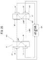
- FIG. 29(a) is a conceptual view illustrative of an example configuration of an NDIR gas sensor according to a first conventional example.
- the NDIR gas sensor includes a gas cell 910, a light source 920 that emits infrared rays with a wavelength corresponding to an absorption wavelength band specific to a gas, and an infrared ray sensor 930 capable of detecting an intensity of light in this wavelength band.
- the light source 920 and the infrared ray sensor 930 are disposed in the gas cell 910.
- the target gas to be measured flows or is accumulated in the gas cell 910 to that the concentration of the target gas to be measured is obtained from the amount of infrared rays absorbed by a space between the light source 920 and the infrared sensor 930 in the gas cell.
- the intensity of the light source of the NDIR gas sensor changes, the absolute value of the concentration of the measured gas drifts, making impossible an accurate measurement of the concentration.
- PTL 2 discloses an NDIR gas sensor using two wavelength bands.
- the gas sensor of PTL 2 includes two light sources so that light with a wavelength absorbed by a detection target gas and light with a wavelength not absorbed by the detection target gas are caused to pass through a gas cell in order to measure a concentration of a gas to be detected based on output ratios of the sensors.
- a typical NDIR sensor uses a band-pass filter with transmittance only on a specific wavelength band.
- a detection target gas is detected by using a reference band-pass filter f'1 transmissive to light in a wavelength band of about 3.9 ⁇ m that is substantially not absorbed by carbon dioxide and a band-pass filter f'2 for absorption wavelength transmissive only to light in a wavelength band around 4.3 ⁇ m (4.3 ⁇ m ⁇ (100 to 300 nm)) that is absorbed by carbon dioxide.
- two band-pass filters i.e.
- a technique of increasing an optical path length may be employed. This technique, however, increases the size of the entire sensor and, in addition, attenuation of light from the light sources increases so that an S/N ratio of a signal detected by the sensor decreases, and a variation in measurement by the gas sensor increases. As a result, it is difficult to obtain a gas sensor with high accuracy.
- the present invention has been made in view of the foregoing problems, and has an object of providing a small-size reliable gas sensor that can reduce a measurement error and has a simple configuration.
- An inventor of the present invention has intensively studied to solve the problems described above, to conceive a gas sensor as follows.
- a gas sensor is characterized by including: a first light source; a first sensor unit and a second sensor unit disposed to receive light output from the first light source; a first substrate having a first principal surface and a second principal surface opposite to the first principal surface, the first light source and the first sensor unit being provided on the first principal surface of the first substrate; and a second substrate having a first principal surface and a second principal surface opposite to the first principal surface, the second sensor unit being provided on the first principal surface of the second substrate, wherein the first sensor unit is disposed at a location where light output from the first light source and reflected on the second principal surface of the first substrate strikes the first principal surface of the first substrate.
- the gas sensor may be characterized by further including a computation unit configured to receive an output signal from the first sensor unit and an output signal from the second sensor unit.
- the gas sensor may be characterized in that the first sensor unit and the second sensor unit have an identical temperature characteristic.
- the gas sensor may be characterized by further including a control layer disposed on the second principal surface of the first substrate, and configured to control an amount of light output from the first light source and scattered in the first substrate and an amount and a radiation angle of light output from the first light source and radiated from the second principal surface of the first substrate to a space in the gas cell.
- a control layer disposed on the second principal surface of the first substrate, and configured to control an amount of light output from the first light source and scattered in the first substrate and an amount and a radiation angle of light output from the first light source and radiated from the second principal surface of the first substrate to a space in the gas cell.
- the gas sensor may be characterized in that the laminated structure is a diode structure including a least two types of layers of a p-type semiconductor and an n-type semiconductor and include indium or antimony.
- the gas sensor may be characterized in that each of the first sensor unit and the second sensor unit includes a plurality of light-receiving portions having an identical structure, and the number of light-receiving portions of the first sensor unit is different from that of the second sensor unit.
- the gas sensor may be characterized by further including a second light source disposed on the first principal surface of the second substrate, wherein the second sensor unit is at a location where light output from the second light source and reflected on the second principal surface of the second substrate strikes the second sensor unit.
- the gas sensor may be characterized in that, while the light reception/emission control unit supplies electric power to a light-emitting portion of one of the first light source or the second light source, the light reception/emission control unit does not supply electric power to a light-emitting portion of the other.
- the gas sensor may be characterized in that the light reception/emission control unit controls electric power to be supplied to the first light source and electric power to be supplied to the second light source in such a manner that the first sensor unit and the second sensor unit temperatures become identical.
- the gas sensor may be characterized in that the light reception/emission control unit includes a first temperature measuring unit configured to measure a temperature of the first sensor unit, and a second temperature measuring unit configured to measure a temperature of the second sensor unit.
- the gas sensor may be characterized in that the light reception/emission control unit, calculates a temperature of the first sensor unit based on a resistance value of the first sensor unit, and calculates a temperature of the second sensor unit based on a resistance value of the second sensor unit.
- a small-size and reliable gas sensor that can reduce measurement error and has a simple configuration can be provided.
- the present embodiment An embodiment for carrying out the present invention (hereinafter referred to as the present embodiment) will be described.
- a gas sensor including one light source will be described.
- a gas sensor including two or more light sources will be described.
- other specific aspects (i.e., specific examples) of the present embodiment, first through twenty-first embodiments will be described.
- This configuration enables precise compensation for a change with time due to degradation of a first light source output and an output variation depending on temperature during operation, without providing an optical filter (e.g., a band-pass filter) on an optical path extending from the first light source to the first sensor unit.
- an optical filter e.g., a band-pass filter
- the gas sensor of the first aspect preferably further includes a computation unit that receives an output signal from the first sensor unit and an output signal from the second sensor unit. Based on the output signal from the first sensor unit and the output signal from the second sensor unit, a gas concentration can be computed.
- a computation of a gas concentration may consist on a computation of an absolute value of a gas concentration in the air, or a computation for determining whether the gas concentration exceeds a predetermined threshold.
- the first sensor unit and the second sensor unit preferably have an identical laminated structure, and are preferably formed at the same time (i.e., layers constituting the laminated structures are formed at the same time for the first sensor unit and the second sensor unit).
- the areas in the substrates occupied by the first sensor unit and the second sensor unit may differ from each other.
- an S/N ratio minimum resolution of a gas concentration indicated value
- the light-receiving surface area of the first sensor unit can be reduced, and the area occupied by the first light source can be increased accordingly.
- the S/N ratio of the entire gas sensor can be enhanced.
- the ratio (n : m) in the number of light-receiving portions can be about 1/500, may be about 1/100 or about 1/10, depending on the situation.
- the ratio in the number of light-receiving portions is preferably designed depending on the design of the gas cell or light-emission performance of the first light source.
- a material for the first sensor unit, the second sensor unit, and the first light source is preferably a Group III-V based compound semiconductor, more preferably a compound semiconductor composed of at least one type of Group III elements selected from the group consisting of indium (In), aluminium (Al), and gallium (Ga) and at least one type of Group V atoms selected from the group consisting of antimony (Sb) and arsenic (As), and much more preferably a compound semiconductor including at least one of InSb, AlInSb, GaInSb, or AsInSb.
- a detection target gas is CO 2
- AlInSb or GaInSb can be used for detecting CO 2 absorption around a wavelength of 4.3 ⁇ m.
- AsInSb is preferably used.
- the first light source is formed on the first principal surface of the first substrate.
- the first light source is not specifically limited as long as the first light source outputs light including a wavelength that can be absorbed by a detection target gas.
- a specific configuration of the first light source may be any configuration as long as the first light source can be formed on the first principal surface of the first substrate.
- Specific examples of the first light source include a MEMS and an LED. Among these devices, from the viewpoint of reducing noise due to light absorption of a mixture except the target gas, it is preferable that the first light source outputs only light in a wavelength band showing a large degree of absorption by a detection target gas.
- a LED structure is preferable in some cases because its emission wavelength band can be controlled by changing the band gap in the active layer.
- a band-pass filter does not need to be provided on an optical path extending from the first light source to the first sensor unit (serving as a reference sensor), and thus, accurate compensation for an output variation can be obtained even with the use of a first light source that outputs only light in a wavelength band that can be greatly absorbed by the detection target gas.
- the first light source preferably includes a laminated structure portion having a PN junction or a PIN junction deposited by a deposition method such as molecular beam epitaxy (MBE) or chemical vapor deposition (CVD).
- a deposition method such as molecular beam epitaxy (MBE) or chemical vapor deposition (CVD).
- MBE molecular beam epitaxy
- CVD chemical vapor deposition
- the laminated structure portion operates as a light emitting diode (LED), and can emit light with a wavelength in accordance with a band gap of a material for the laminated structure portion.
- the laminated structure portion (called an active layer) includes In or Sb, light in an infrared region (i.e., infrared rays) can be emitted.
- the use of InSb, InAlSb, or InAsSb for the active layer allows light with a wavelength of 1 to 10 ⁇ m to be output.
- a detection target gas is carbon dioxide
- a carbon dioxide gas shows a large degree of absorption around a wavelength of 4.3 ⁇ m
- InAlSb is preferably used for the active layer.
- the gas sensor can have high sensitivity and high resolution.
- a gas e.g. , vaporized alcohol showing absorption around 10 ⁇ m
- CO bonds showing absorption around 10 ⁇ m
- the use of the first light source of the LED enables detection of a specific gas without using an optical filter (e.g. , a band-pass filter) by tuning a band gap of a material used for a light-emitting layer at an absorption wavelength of the detection target gas.
- an optical filter e.g. , a band-pass filter
- tuning a band gap of a material used for a light-emitting layer at an absorption wavelength of the detection target gas e.g. , a band-pass filter
- the first sensor unit is provided on the first principal surface of the first substrate.
- the location of the first sensor unit is not specifically limited as long as light output from the first light source and reflected on the second principal surface opposite to the first principal surface of the first substrate strikes the first sensor unit.
- the laminated structure of the first sensor unit can be a diode structure having a PN junction or a PIN junction, and may include indium, antimony or either of these materials.
- the laminated structure may further include a mixed crystal-based material further including at least one material selected from the group consisting of Ga, Al, and As, depending on the absorption wavelength of the detection target gas.
- the material and the laminated structure of a light-receiving element of the first sensor unit are preferably similar to the material and the laminated structure of the first light source.
- the first sensor unit of the present embodiment preferably has a configuration in which light-receiving elements are connected in series.
- the first light source and the first sensor unit are disposed on the first substrate, an amount of light incident on the first sensor unit tends to be larger than an amount of light incident on the second sensor unit.
- the total area of the light-receiving portions of the first sensor unit can be made smaller than the total area of the light-receiving portions of the second sensor unit. In this manner, the size of the gas sensor can be further reduced.
- the second substrate is not specifically limited as long as the second sensor unit is provided on the first principal surface. Light incident from the second principal surface passes through the inside of the second substrate, and strikes the second sensor unit.
- a material for the second substrate is not specifically limited.
- a Si substrate, a GaAs substrate, or a sapphire substrate may be used, but the material for the second substrate is not limited to these materials.
- the material for the second substrate is preferably a material highly transmissive to light incident from the second principal surface.
- the second substrate is preferably disposed to be adjacent to the first substrate with side surfaces thereof facing each other and a light-blocking portion is preferably disposed between the first substrate and the second substrate.
- the thus-configured gas sensor preferably includes a light reflection unit described later.
- the light-blocking portion described above is preferably disposed at a joint portion between the first substrate and the second substrate.
- the light-blocking portion is preferably provided because the light-blocking portion can prevent light output from the first light source from striking the second sensor unit without passing a space in the gas cell.
- detection sensitivity a signal change due to a change in gas concentration
- the second sensor unit is not specifically limited as long as the second sensor unit is disposed on the second substrate.
- the second sensor unit and the first sensor unit are preferably formed on an identical substrate in their fabrication process, and more preferably have an identical laminated structure.
- the laminated structure of the second sensor unit is preferably a diode structure including a PN junction or a PIN junction and includes a material of indium or antimony.
- an optical filter transmissive only to light in a specific wavelength band is preferably provided on an optical path along which light radiated from the second principal surface of the first substrate strikes the second sensor unit.
- the presence of the optical filter is especially preferable.
- the first substrate provided with the first sensor unit and the second substrate provided with the second sensor unit are originally made from the same wafer.
- the first sensor unit and the second sensor unit have similar laminated structures, variations in sensitivity characteristic and temperature characteristic of sensitivity between the first sensor unit and the second sensor unit are reduced, thereby enhancing advantages of the present invention.
- the sensitivity of the first sensor unit is Ri2 ( ⁇ ) [A/W] and the sensitivity of the second sensor unit 2 is Ri2 ( ⁇ ) [A/W]
- /(Ri1 ( ⁇ )) only needs to be within 20%, preferably less than or equal to 10%, and much more preferably less than or equal to 5%.
- the gas sensor of the first aspect preferably includes a light reflection unit in a space of the gas cell facing the second principal surfaces of the first substrate and the second substrate. That is, a light reflection unit is preferably provided at a location separated from the first substrate and the second substrate in the gas cell and facing the second principal surface of the first substrate and the second principal surface of the second substrate.
- the light reflection unit preferably reflects light radiated from the second principal surface of the first substrate and causes the reflected light to strike the second sensor unit.
- the light reflection unit is preferably a light-collecting type light reflection unit.
- All the light emitted from the first light source and input to the second sensor unit is preferably light that has passed through the space in the gas cell.
- a technique of disposing the first substrate provided with the first light source and the first sensor unit and the second substrate provided with the second sensor unit in such a manner that the first substrate is opposite to the second substrate may be employed.
- the first substrate and the second substrate are preferably disposed adjacent each other with their side surfaces facing each other.
- a light-blocking portion is preferably provided between the first substrate and the second substrate.
- the gas sensor of the second aspect further includes a second light source provided on a first principal surface of a second substrate, in addition to the configuration of the gas sensor of the first aspect.
- the second sensor unit is preferably disposed at a location where light emitted from the second light source and reflected on a second principal surface opposite to a first principal surface of the second substrate strikes the second sensor unit.
- This configuration allows light output from the first light source to pass through an optical path in a first substrate serving as an environment independent of the presence of a gas and a concentration of the gas, for example, and to strike a first sensor unit (a light-receiving element for monitoring when viewed from the first light source).
- a first sensor unit a light-receiving element for monitoring when viewed from the first light source.
- light output from the second light source passes through the optical path in the second substrate serving as an environment independent of the presence of a gas and a concentration of the gas, for example, and strikes the second sensor unit (a light-receiving element for monitoring when viewed from the second light source).
- the second sensor unit a light-receiving element for monitoring when viewed from the second light source.
- the first sensor unit and the second sensor unit preferably have an identical temperature characteristic.
- the "identical temperature characteristic” refers to a state in which a temperature characteristic is generally uniform to such a degree that does not hinder advantages of the present invention.
- an output signal from the first sensor unit is S1 and an output signal from the second sensor unit is S2 under a sensor temperature Tx in a typical operating temperature range (e.g., a range from 0°C to 50°C) of a gas sensor.
- a/b is preferably greater than or equal to 0.8 and less than or equal to 1.2, more preferably greater than or equal to 0.9 and less than or equal to 1.1, and much more preferably greater than or equal to 0.99 and less than or equal to 1.01, per 1°C.
- a ratio between a maximum value and a minimum value of a ratio (a/b[/°C]) between an output coefficient a of change of the first sensor unit per 1°C and an output coefficient b of change of the second sensor unit per 1°C is preferably greater than or equal to 0.8 and less than or equal to 1.2. This is because in this range, variations in signals of emitted light and received light can be compensated for based on the output of the first sensor unit, independently of the application environmental temperature of the gas sensor, even in a case where a light emission characteristic of the first light source changes so that the state of a space can be correctly detected by using the second sensor unit.
- variations in signals of emitted light and received light can be compensated based on the output of the second sensor unit, independently of the environmental temperature of the gas sensor so that the state of the space can be correctly detected by using the first sensor unit.
- output coefficients (a and b) of changes of the first sensor unit and the second sensor unit obtained when the temperatures of the first sensor unit and the second sensor unit change from 0°C to 50°C are obtained. Then, an a/b/ ⁇ T ratio with a temperature change of ⁇ T is calculated. In this manner, the ratio in coefficient of change between the outputs per 1°C described above can be determined.
- a method for setting the maximum value and the minimum value of the ratio in coefficient of change between the outputs of the first sensor unit and the second sensor unit per 1°C in the range described above can be a method of forming the first sensor unit and the second sensor unit in such a manner that the first sensor unit and the second sensor unit have an identical laminated structure made of an identical material.
- the first sensor unit and the second sensor unit have theoretically identical temperature characteristic.
- the first sensor unit and the second sensor unit preferably have an identical laminated structure, and are preferably formed at the same time (i.e. , layers constituting the laminated structures are formed at the same time for the first sensor unit and the second sensor unit).
- the first sensor unit and the second sensor unit are formed on the identical substrate, made of the identical material by the same process at the same time, the first sensor unit and the second sensor unit have an identical spectral sensitivity characteristic and an identical temperature characteristic, thereby enhancing advantages of the present invention.
- the spectral sensitivity characteristic refers to sensitivity at each wavelength.
- an optical filter e.g., a band-pass filter
- the optical filter can obtain a transmission characteristic (several tens of nanometers to several hundreds of nanometers) having a narrow full width at half maximum, thereby easily selecting a specific wavelength.
- the first sensor unit and the second sensor unit preferably have large numbers of light-receiving portions with an identical configuration in such a manner that the number of light-receiving portions, and the number of light-receiving portions of the first sensor unit is preferably equal to that of the second sensor unit.
- the state of the space formed from a light-emitting portion to the sensor unit is detected (e.g., a concentration of a detection target substance in the space is calculated).
- the minimum resolution of the gas sensor is determined based on the S/N ratios of the first sensor unit and the second sensor unit.
- a light reception/emission control unit that supplies electric power to the first light source and the second light source and detects output signals from the first sensor unit and the second sensor unit. While the light reception/emission control unit supplies electric power to the light-emitting portion of one of the first light source or the second light source, the light reception/emission control unit does not need to supply electric power to the light-emitting portion of the other.
- the light reception/emission control unit may supply an identical level of electric power to the first light source and the second light source. Alternatively, the light reception/emission control unit may control electric power to be supplied to the first light source and electric power supplied to the second light source in such a manner that the first sensor unit and the second sensor unit are at an identical temperature. Embodiments using light reception/emission control units will be described later.
- the output signal from the first sensor unit is equal to the output signal from the second sensor unit.
- the first light source and the second light source are made of compound semiconductor laminated portions having an identical structure and an identical composition
- the light reception/emission control unit alternately drives the first light source and the second light source or supplies an identical level of electric power to the first light source and the second light source
- the amount of heat generated by the first light source and the amount of heat generated by the second light source are steadily the same so that the first light source and the second light source are at an identical temperature.
- SNR TRASM SNR 12 1 / 2 + SNR 21 1 / 2 1 / 2
- Equation (1) and Equation (2) demonstrate that light emission and reception performed in both directions can enhance the SNR of a system, as compared to the case of performing light emission and reception in one direction.
- Examples of a signal obtained from the first sensor unit include a signal Ip_ REF_1 in a case where the first light source emits light and a signal Ip _TRASM_2 in a case where the second light source emits light.
- Examples of a signal obtained from the second sensor unit include a signal Ip_ REF_2 in a case where the second light source emits light and a signal Ip _TRASM_1 in a case where the first light source emits light.
- the output signal ratios (Ip _TRASM_1 /Ip _REF_1 ) and (Ip _TRASM_2 /Ip_ REF_2 ) change depending on material properties of the first substrate and the second substrate, processing methods for the second principal surface of the first substrate and the second principal surface of the second substrate, and the presence and optical properties of a control layer formed on the second principal surface of the substrate described later, for example.
- the first substrate includes the first light source and the first sensor unit on the first principal surface.
- the second substrate includes the second light source and the second sensor unit on the first principal surface.
- a material for the first substrate and the second substrate include Si, GaAs, sapphire, InP, InAs, and Ge.
- the material for the first substrate and the second substrate is not limited to these materials, and may be selected in accordance with a wavelength band used.
- a semi-insulating substrate is preferably used for each of the first substrate and the second substrate. From the viewpoint of capability of fabricating a semi-insulating substrate and increasing an opening diameter, a GaAs substrate is especially preferable.
- the material for each of the first substrate and the substrate is preferably a material highly transmissive to light output from the light-emitting portion.
- the material for each of the first substrate and the second substrate is preferably a material with which light output from the light-emitting element is efficiency reflected on the second principal surface.
- a GaAs substrate is preferable.
- a material used for each of the first sensor unit, the second sensor unit, the first light source, and the second light source is preferably a Group III-V compound semiconductor, more preferably a compound semiconductor composed of at least one type of Group III atoms selected from the group consisting of indium (In), aluminium (Al), and gallium (Ga) and at least one type of Group V atoms selected from the group consisting of antimony (Sb) and arsenic (As), and much more preferably a compound semiconductor including at least one of InSb, AlInSb, GaInSb, or AsInSb.
- a detection target gas is CO 2 .
- AlInSb or GaInSb can be used as a material for each of the first sensor unit, the second sensor unit, the first light source, and the second light source.
- a longer wavelength (9 to 10 ⁇ m) is needed.
- AsInSb is preferably used for each of the first sensor unit, the second sensor unit, the first light source, and the second light source.
- first sensor unit, the second sensor unit, the first light source, and the second light source are made of a compound semiconductor having an identical film composition (i.e., a compound semiconductor laminated portion having an identical composition)
- advantages of the present invention can be maximized.
- the identical film composition can be obtained by laminating films on the same substrate by the same process. That is, the first sensor unit, the second sensor unit, the first light source, and the second light source are preferably formed on the same wafer in some cases.
- a pair of chips that are adjacent in a wafer plane are preferably incorporated in the same gas sensor in some cases. This configuration can reduce the composition deviation generated during a deposition process, in an assembled gas sensor, can make the first sensor unit and the second sensor unit have an identical temperature characteristic, and make the first light source and the second light source have an identical temperature characteristic, thereby enabling accurate temperature compensation.
- a control layer is preferably provided on the second principal surface of the first substrate and the second principal surface of the second substrate in some cases.
- the control layer is a layer for controlling an amount and a reflection/scattering angle of light scattered in the substrate and an amount and a radiation angle of light output from the light-emitting element and radiated from the second principal surface of the substrate to an optical path (e.g., a gas cell in the case of a gas sensor).
- the control layer is provided on the second principal surface of the first substrate and the second principal surface of the second principal surface so that the gas sensor can be designed to increase the S/N ratio of the entire sensor (to obtain a high resolution).
- the control layer include an anti-reflection film, a laminated film composed of a large number of materials having different refractive indexes, a coarsed layer, and a combination thereof.
- the first light source is formed on the first principal surface of the first substrate
- the second light source is formed on the first principal surface of the second substrate.
- the first light source and the second light source are not specifically limited as long as the first light source and the second light source output light including wavelengths absorbed in a detection target substance (e.g., a gas).
- Configurations of the first light source and the second light source are not specifically limited as long as the first light source and the second light source can be formed on the first principal surface of the first substrate and the first principal surface of the second substrate. Specific examples thereof include a MEMS and an LED.
- each of the first light source and the second light source preferably outputs only light in a wavelength band that can be greatly absorbed by a detection target substance.
- a LED structure is preferable in some cases because an emission wavelength band is controlled by using a band gap in an active layer.
- the light-emitting element preferably includes a laminated structure portion including a PN junction or a PIN junction deposited by a deposition method such as molecular beam epitaxy (MBE) or chemical vapor deposition (CVD).
- the laminated structure portion operates as a light emitting diode (LED), and can emit light with a wavelength in accordance with a band gap of a material for the laminated structure portion.
- the laminated structure portion (called an active layer) includes In or Sb
- In or Sb light in an infrared region (i.e., infrared rays) can be emitted.
- InSb, InAlSb, or InAsSb for the active layer enables light emission with a wavelength of 1 to 12 ⁇ m.
- a narrow band gap material in which an active layer includes In and/or Sb generally has a large temperature characteristic (a change in light emission characteristic due to a temperature of a light-emitting element itself).
- the gas sensor of the second aspect can always correctly monitor even a large change in light emission characteristic, and can always obtain a constant light emission characteristic by controlling an operation of the light-emitting element based on a result of the monitoring.
- the first sensor unit is formed on the first principal surface of the first substrate, and the second sensor unit is formed on the first principal surface of the second substrate.
- the first sensor unit is disposed at a location where light output from the first light source and reflected on the second principal surface opposite to the first principal surface of the first substrate strikes the first sensor unit.
- the second sensor unit is disposed at a location where light output from the second light source and reflected on the second principal surface opposite to the first principal surface of the second substrate strikes the second sensor unit.
- a length of an optical path P11 to the first sensor unit is L11
- a length of an optical path P12 to the second sensor unit is L12.
- a length of an optical path to the second sensor unit is L22
- a length of an optical path P21 to the first sensor unit is L21.
- the gas sensor is preferably designed in such a manner that in accordance with a concentration and an absorptance of a detection target substance of the gas sensor, transmission characteristics of the optical path P12 and the optical path P21 preferably change accordingly.
- the lengths L12 and the L21 are preferably designed at maximum.
- the laminated structure of each of the first sensor unit and the second sensor unit is a diode structure having a PN junction or a PIN junction, and may include a material of indium or antimony.
- the diode structure may include a mixed crystal-based material in which a material of indium or antimony further includes at least one material selected from the group consisting of Ga, Al, and As.
- the material and the laminated structure of the light-receiving element of the first sensor unit are preferably similar to the material and the laminated structure of the light-emitting element of the second sensor unit.
- the first sensor unit and the second sensor unit of the present embodiment are preferably configured in such a manner that a plurality of light-receiving elements are serially connected to each other. This is because the presence of a large number of light-receiving elements can increase an internal resistance of the entire sensor unit so that, when the sensor unit is connected to an amplifier, a high S/N ratio can be obtained.
- the first substrate provided with the first sensor unit and the second substrate provided with the second sensor unit are originally (i.e. , before dicing) made from the same wafer.
- the first sensor unit and the second sensor unit preferably have similar laminated structures. In this manner, variations in sensitivity characteristic and temperature characteristic of sensitivity between the first sensor unit and the second sensor unit are suppressed, thereby enhancing advantages of the present invention. Specifically, suppose the sensitivity of the first sensor unit is Ri1 ( ⁇ ) [A/W] and the sensitivity of the second sensor unit is Ri2 ( ⁇ ) [A/W].
- a light reflection unit is preferably provided in a space outside the substrates facing the second principal surface of the first substrate and the second principal surface of the second substrate. That is, a light reflection unit is preferably provided at a location separated from the first substrate and the second substrate in the gas cell and facing the second principal surface of the first substrate and the second principal surface of the second substrate.
- the light reflection unit preferably reflects light emitted from the second principal surface of the first substrate and causes the reflected light to strike the second sensor unit.
- the light reflection unit preferably reflects light emitted from the second principal surface of the second substrate and causes the reflected light to strike the first sensor unit.
- the light reflection unit is preferably a light-collecting type light reflection unit.
- All the light output from the first light source and incident on the second sensor unit and all the light output from the second light source and incident on the first sensor unit are preferably light that has passed through a space outside the substrates (external space).
- a technique of disposing the first substrate provided with the first light source and the first sensor unit and the second substrate provided with the second sensor unit in such a manner that the first substrate and the second substrate face each other may be employed.
- a technique of disposing the second substrate provided with the second light source and the second sensor unit and the first substrate provided with the first sensor unit in such a manner that the first substrate and the second substrate face each other may be employed. That is, the first substrate and the second substrate preferably face each other.
- the first substrate and the second substrate are preferably disposed adjacent to each other with their side surfaces facing each other.
- a signal change depending on a change of state of the external space can serve as a signal component (offset) that does not depend on a change of state of the external space, leading to the possibility of a decrease in measurement sensitivity of the gas sensor.
- a light-blocking portion is preferably provided between the side surfaces of the first substrate and the second substrate.
- the first substrate and the second substrate are independent of each other.
- the first sensor unit, the second sensor unit, the first light source, and the second light source may be formed on a first principal surface of a common substrate.
- the substrate is designed in such a manner that the first sensor unit is formed near a first light source and a second sensor unit is formed near the second light source.
- the first aspect has advantages (1) to (4) as follows:
- the second aspect has advantages (5) to (8) as follows:
- width-to-length dimensions are preferably less than or equal to 20 x 20 mm 2 , more preferably less than or equal to 15 x 15 mm 2 , much more preferably less than or equal to 10 x 10 mm 2
- a height is preferably less than or equal to 10 mm, more preferably less than or equal to 5 mm, and much more preferably less than or equal to 3 mm.
- a gas sensor having such dimensions is also enabled to have high sensitivity and high accuracy.
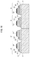
- the first sensor unit 31 is disposed at a location where light output from the first light source 20 and reflected on the second principal surface 412 opposite to the first principal surface 411 of the first substrate 41 (indicated by broken lines) strikes the first sensor unit 31.
- the gas sensor can have a simple configuration, a small size and high reliability and obtain constant compensation for a measurement error due to a change in emission intensity of the first light source 20, independently of an application environment.
- a first substrate 41 and a second substrate 42 are disposed adjacent to each other with side surfaces (i.e., parts of peripheral side surfaces) thereof facing each other.
- Such a layout herein will be hereinafter referred to as a parallel layout.
- the second embodiment is different from the first embodiment in that the first substrate 41 and the second substrate 42 are disposed in a parallel layout.
- the other part of the configuration of the second embodiment is the same as that of the first embodiment.
- a part of an inner wall of a gas cell 10 is preferably covered with a material having a high reflectance especially in the second embodiment and the third, fifth, and sixth embodiments
- FIG. 3 is a conceptual illustration of an example configuration of a gas sensor according to a third embodiment of the present invention.
- this gas sensor includes a light-blocking portion 50 provided between a first substrate 41 and a second substrate 42.
- the third embodiment is different from the second embodiment in including the light-blocking portion 50.
- the light-blocking portion 50 may be made of an encapsulating resin.
- the other part of the configuration of the third embodiment is the same as that of the second embodiment.
- the gas sensor of the fourth embodiment includes the light reflection unit 60 so that infrared rays (indicated by dot-and-dash lines) emitted from the second principal surface 412 of the first substrate 41 and included in light output from a first light source 20 are reflected on the light reflection unit 60 and selectively strike the second sensor unit 32.
- the gas sensor is enabled to have high sensitivity.
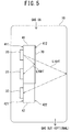
- FIG. 5 is a conceptual illustration of an example configuration of a gas sensor according to a fifth embodiment of the present invention.
- this gas sensor includes a control layer 70 that is disposed on a second principal surface 412 of a first substrate 41 and controls an amount of light (indicated by dotted lines) output from a first light source 20 and scattered in the first substrate 41 and an amount of a radiation angle of light (indicated by dot-and-dash lines) output from the first light source 20 and radiated from the second principal surface 412 of the first substrate 41 to a space in a gas cell 10.
- the fifth embodiment is different from the second embodiment in including the control layer 70.
- the other part of the configuration of the fifth embodiment is the same as that of the second embodiment.
- the gas sensor of the fifth embodiment includes the control layer 70 so that a ratio between an amount of light desired to strike a first sensor unit 31 and an amount of light desired to strike a second sensor unit 32.
- the control layer 70 may be provided on a second principal surface of a second substrate 42.
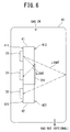
- FIG. 6 is a conceptual illustration of an example configuration of a gas sensor according to a sixth embodiment of the present invention.
- this gas sensor includes a light reflection layer 701 disposed on a second principal surface of a first substrate and reflects light output from a first light source toward a first sensor unit.
- a material for the light reflection layer 701 may be any material as long as the material reflects light, and a material showing a metallic luster and total internal reflection is more preferable. Specifically, from the viewpoint of high reflectance, a material including Al and/or Au is preferable in some cases.
- the sixth embodiment is different from the second embodiment in including the light reflection layer 701. The other part of the configuration of the sixth embodiment is the same as that of the second embodiment.
- the gas sensor of the sixth embodiment includes the light reflection layer 701 so that an amount of light desired to strike a first sensor unit 31 can be enhanced. In this manner, a signal S/N ratio of the first sensor unit 31 can be enhanced. In some cases, the light-receiving surface area of the first sensor unit can be reduced with the S/N ratio being kept so that an efficiency in using a substrate can be enhanced.
- FIG. 7 is a sectional view illustrating an example configuration of a gas sensor according to a seventh embodiment of the present invention.
- reference numerals 201, 311, and 321 denote a semiconductor layer of a first conductivity type (e.g., an n-type semiconductor layer)
- reference numerals 202, 312, and 322 is a semiconductor layer of a second conductivity type (e.g., a p-type semiconductor layer)
- reference numerals 203, 204, 313, 314, 323, and 324 denote electrodes.
- a first sensor unit 31 includes, for example, the semiconductor layer 311 of the first conductivity type formed on the first principal surface 411 of the first substrate 41, the semiconductor layer 312 of the second conductivity type and the electrode 313 formed on the semiconductor layer 311, and the electrode 314 formed on the semiconductor layer 312.
- a second sensor unit 32 includes, for example, the semiconductor layer 321 of the first conductivity type formed on a first principal surface 421 of a second substrate 42, the semiconductor layer 322 of the second conductivity type and the electrode 323 formed on the semiconductor layer 321, and the electrode 324 formed on the semiconductor layer 322.
- the semiconductor layers 201, 311, and 321 of the first conductivity type are made of an identical material and have an identical thickness, for example.
- the semiconductor layers 202, 312, and 322 of the second conductivity type are made of an identical material and have an identical thickness.
- each of the first sensor unit 31 and the second sensor unit 32 is illustrated as one element.
- a plurality of elements may be electrically connected to each other so that the elements can serve as one sensor unit.
- a first light source 20 may be a plurality of elements that are electrically connected to each other.
- An intrinsic semiconductor layer (a so-called i-type semiconductor layer) may be inserted between the semiconductor layers 201, 311, and 321 of the first conductivity type and the semiconductor layers 202, 312, and 322 of the second conductivity type so that a PIN junction is formed.
- the gas sensor of the seventh embodiment includes the semiconductor layers 201, 311, and 321 of the first conductivity type and the semiconductor layers 202, 312, and 322 of the second conductivity type made of identical or similar materials and having identical or similar thicknesses so that the first light source 20, the first sensor unit 31, and the second sensor unit 32 show an identical temperature characteristic.
- the gas sensor has high accuracy, independently of a change in the environmental temperature.
- FIG. 8 is a conceptual illustration of an example configuration of a gas sensor according to an eighth embodiment of the present invention.
- FIG. 9 is a conceptual illustration of an example configuration of a gas sensor according to a ninth embodiment of the present invention.
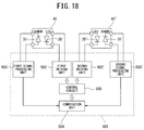
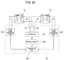
- each of the first substrate 41 and the second substrate 42 of the gas sensor of the first embodiment is encapsulated by an encapsulating resin 200, and a driving unit and a signal processing unit are connected to a first light source 20, a first sensor unit 31, and a second sensor unit 32.
- the gas sensor of the ninth embodiment includes a light source power supply unit 101 for supplying electric power to the first light source 20, and a gas concentration computing unit 104 that receives signals output from the first sensor unit 31 and the second sensor unit 32 and compute a gas concentration of a detection target gas.
- the light source power supply unit 101 preferably supplies a pulse signal (voltage or current) to the first light source 20.
- the driving unit and the signal processing unit are connected to the first light source 20, the first sensor unit 31, and the second sensor unit 32 so that a gas concentration of a detection target gas introduced into a gas cell 10 can be automatically calculated and a result of the calculation can be output.
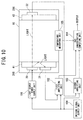
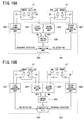
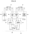
- FIG. 10 is a conceptual illustration of an example configuration of a gas sensor according to a tenth embodiment of the present invention.
- this gas sensor further includes, in addition to the components of the gas sensor of the ninth embodiment, a first amplifying unit 102 for amplifying an output signal from a first sensor unit 31, a second amplifying unit 103 for amplifying an output signal from a second sensor unit 32, a temperature measuring unit 105 for measuring a temperature in a gas cell 10, and a driving signal supply unit 106 for supplying driving signals to the light source power supply unit 101, the first amplifying unit 102, and the second amplifying unit 103.
- a first amplifying unit 102 for amplifying an output signal from a first sensor unit 31
- a second amplifying unit 103 for amplifying an output signal from a second sensor unit 32
- a temperature measuring unit 105 for measuring a temperature in a gas cell 10
- a driving signal supply unit 106 for supplying driving signals to the light source power supply unit 101, the first amplifying unit 102, and the second amplifying unit 103.
- a signal supplied from the driving signal supply unit 106 is preferably a pulsed synchronizing signal for determining operation timings of the light source power supply unit 101, the first amplifying unit 102, and the second amplifying unit 103.
- the temperature measuring unit 105 for measuring a temperature around or in the gas cell 10 is preferably provided.
- An emission spectrum of the first light source 20 can change depending on an environmental temperature in some cases.
- the amount of light absorption can change depending on an environmental temperature in some cases.
- the temperature measuring unit 105 is preferably provided because temperature information obtained by the temperature measuring unit 105 can be supplied to the gas concentration computing unit 104 so that compensation for a shift depending on an environmental temperature can be obtained.
- each of the first amplifying unit 102 and the second amplifying unit 103 is preferably an amplifier (a so-called Lock-in Amp) having a phase shift detection (PSD) function.
- an output signal from the driving signal supply unit 106 is preferably a pulsed synchronizing signal.
- a detection target gas introduced into the gas cell 10 is a mixed gas of a gas A and a gas B
- the gas A is absorbed in the wavelength 1 and the wavelength 2 and the gas B is similarly absorbed in the wavelength 1 and the wavelength 2, but an absorption ratio differs between the gas A and the gas B.
- This case uses a gas sensor having a configuration in which the second substrate 42 includes the band-pass filter f1 transmissive to light with the wavelength 1 and the second substrate 42' includes the band-pass filter f2 transmissive to light with the wavelength 2.
- the temperature characteristics may differ between the sensors.
- a temperature characteristic g1(T) of the first sensor unit is equal to, or in proportion to, a temperature characteristic g2(T) of the second sensor unit, Ip2/Ip1 ⁇ (1-A(C)) is established, and temperature dependency of the gas sensor can be eliminated.
- an intrinsic absorbance due to gas molecules absorbance can be obtained. From the Lambert-Beer law, a gas concentration C can be extracted from (1-A(C)).
- the amount of the first light source is not indicated in the computation result, and thus, even when the first light source is degraded, that is, the light emission efficiency changes, the gas concentration computation result does not change.
- the first light source 20 and the first sensor unit 31 are formed on the same substrate (the first substrate 41), and a signal based only on light emitted from the first light source 20 can be output. Thus, the amount of light emitted from the first light source 20 can be correctly measured.
- the first light source is constituted by a large number of light-emitting portions
- arrangement of light-receiving portions of the first light source 20 and light-receiving portions of the first sensor unit 31 is appropriately designed so as to enable measurement of quantities of light emitted from the light-emitting portions.
- An offset due to a disturbance or a circuit can be removed by continuously turning the first light source on and off (pulsed driving), reading signals from the first sensor unit and the second sensor unit when the first light source is on and signals from the first sensor unit and the second sensor unit when the first light source is off, and utilizing a signal difference thereof. This is because an offset due to a circuit or a disturbance always occurs irrespective of on/off of the first light source, and thus, the offset component can be removed by taking a signal difference between the on state and the off state.
- the gas cell is designed to have an excessive length in order to reduce power consumption of the entire gas sensor, a sufficient S/N ratio cannot be obtained in some cases. That is, although a short gas path is needed, as the gas path becomes shorter, a change in signal in accordance with temperature becomes more significant rather than a change in signal in accordance with a change in gas concentration. In such case, an effective temperature compensation technique is inevitable.
- the first sensor unit and the second sensor unit are preferably quantum sensors because such quantum sensors can operate at high speed (are responsive to a high-speed optical pulse).
- a quantum sensor since an internal resistance of a sensor changes in accordance with temperature, an internal temperature of the gas sensor can be determined by reading an internal resistance value of this sensor. The use of this technique eliminates the need for additionally providing the temperature measuring unit 105, and thus, the resulting gas sensor can perform temperature compensation with a small number of components.
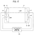
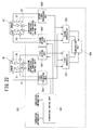
- Light output from the first light source 20 and reflected on the second principal surface 412 opposite to the first principal surface 411 of the first substrate 41 strikes the first sensor unit 31, and light emitted from the second principal surface 412 of the first substrate 41 (indicated by chain lines) strikes the second principal surface 412' of the second substrate 41' and then strikes the second sensor unit 31' through the inside of the second substrate 41'.
- the gas sensor according to the twelfth embodiment includes a light reception/emission control unit 501.
- the light reception/emission control unit 501 supplies electric power to the first light source 20 and the second light source 20', and detects signals output from the first sensor unit 31 and the second sensor unit 31'.
- the light reception/emission control unit 501 supplies a desired level of electric power to each of the first light source 20 and the second light source 20' in such a manner that a temperature of the first sensor unit 31 disposed near the first light source 20 and a temperature of the second sensor unit 31' disposed near the second light source 20' are equal to each other.
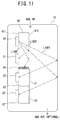
- FIG. 13 is a conceptual illustration of an example configuration of a gas sensor according to a thirteenth embodiment of the present invention.
- a first substrate 41 and a second substrate 41' are disposed adjacent to each other with their side surfaces (i.e., parts of peripheral side surfaces) thereof facing each other.
- Such a layout herein will be hereinafter referred to as a parallel layout.
- the thirteenth embodiment is different from the twelfth embodiment in that the first substrate 41 and the second substrate 41' are disposed in a parallel layout.
- This gas sensor includes a light reflection unit 60 in a space facing a second principal surface 412 of the first substrate 41 and a second principal surface 412' of the second substrate 41'. That is, the gas sensor includes the light reflection unit 60 that is disposed away from the first substrate 41 and the second substrate 41' and reflects light emitted from the second principal surface 412 of the first substrate 41 toward a second sensor unit 31' and also reflects light emitted from the second principal surface 412' of the second substrate 41' toward a first sensor unit 31.
- the thirteenth embodiment is different from the twelfth embodiment in that the first substrate 41 and the second substrate 41' are disposed in a parallel layout and the light reflection unit 60 is provided.
- the other part of the configuration of the thirteenth embodiment is the same as that of the twelfth embodiment.
- the first substrate 41 and the second substrate 41' are disposed in a parallel layout so that the size of the gas sensor can be further reduced.
- the light reflection unit 60 enables light output from the first light source 20 and emitted from the second principal surface 412 of the first substrate 41 (indicated by dot-and-dash lines) to be reflected on the light reflection unit 60 and to selectively strike the second sensor unit 31'.
- the light reflection unit 60 also enables light output from the second light source 20' and emitted from the second principal surface 412' of the second substrate 41' (not shown) to be reflected on the light reflection unit 60 and to selectively strike the first sensor unit 31.
- the resulting gas sensor can have higher sensitivity.
- a light-blocking portion 50 may be provided between the first substrate 41 and the second substrate 41'.
- the light-blocking portion 50 is preferably provided in some cases because the light-blocking portion 50 can prevent light emitted from the first light source 20 from striking the second sensor unit 31' through a side surface of the second substrate 41' and also prevent light emitted from the second light source 20' from striking the first sensor unit 31 through a side surface of the first substrate 41.
- the light-blocking portion 50 may be a part of a resin mold used for encapsulating the first substrate 41 and the second substrate 41'.
- a first light source 20 includes, for example, a semiconductor layer 201 of a first conductivity type (e.g. , n-type) formed on a first principal surface 411 of a first substrate 41, a semiconductor layer 202 of a second conductivity type (e.g., p-type) and an electrode 203 formed on the semiconductor layer 201, and an electrode 204 formed on the semiconductor layer 202.
- a semiconductor layer 201 of a first conductivity type e.g. , n-type
- a semiconductor layer 202 of a second conductivity type e.g., p-type
- a first sensor unit 31 includes, for example, a semiconductor layer 311 of the first conductivity type formed on the first principal surface 411 of the first substrate 41, a semiconductor layer 312 of the second conductivity type and an electrode 313 formed on a semiconductor layer 311, and an electrode 314 formed on the semiconductor layer 312.
- a second sensor unit 31' includes, for example, a semiconductor layer 311' of the first conductivity type formed on the first principal surface 411' of the second substrate 41', a semiconductor layer 312' of the second conductivity type and an electrode 313' formed on the semiconductor layer 311', and an electrode 314' formed on the semiconductor layer 312'.
- the semiconductor layers 201, 311, 201', and 311' of the first conductivity type are made of an identical material and have an identical thickness, for example.
- the semiconductor layers 202, 312, 202', and 312' of the second conductivity type are made of an identical material and have an identical thickness, for example.
- the first light source 20, the second light source 20', the first sensor unit 31, and the second sensor unit 31' include a compound semiconductor having an identical film composition (i.e., compound semiconductor laminated portions having an identical composition).
- the first light source 20 and the second light source 20' have an identical structure (i.e. , have an identical shape and size).
- the first sensor unit 31 and the second sensor unit 31' also have an identical structure.
- the gas sensor of the fifteenth embodiment includes the semiconductor layers 201, 311, 201', and 311' of the first conductivity type made of identical or similar materials and having identical or similar thicknesses and the semiconductor layer 202, 312, 202', and 312' of the second conductivity type made of identical or similar materials and having identical or similar thicknesses so that the first light source 20, the second light source 20', the first sensor unit 31, and the second sensor unit 31' show an identical temperature characteristic.
- the gas sensor has high accuracy, independently of a change in an environmental temperature.
- this gas sensor is an example in which the first substrate 41 and the second substrate 41' of the gas sensor of the twelfth embodiment are respectively encapsulated by an encapsulating resin 200 and an encapsulating resin 200' and a light reception/emission control unit 501 is connected to a first light source 20, a first sensor unit 31, a second light source 20', and a second sensor unit 31'.
- the first substrate 41 and the second substrate 41' are disposed with second principal surfaces 412 and 412' thereof facing each other.
- light output from the first light source 20 and emitted from the second principal surface 412 of the first substrate 41 passes through the space in the gas cell 10, strikes the second principal surface 412' of the second substrate 41', and strikes the second sensor unit 31' through the second substrate 41'.
- Light output from the second light source 20' and emitted from the second principal surface 412' of the second substrate 41' passes through the space in the gas cell 10, strikes the second principal surface 412 of the first substrate 41, and strikes the first sensor unit 31 through the first substrate 41. That is, a space (optical path space) serving as an optical path is present in the gas cell 10.
- FIG. 18 illustrates an example of a circuit configuration in the sixteenth embodiment.
- FIG. 18 illustrates a more specific example configuration of the light reception/emission control unit 501, and a circuit configuration in a case where the first sensor unit 31 and the second sensor unit 31' are photodiodes, and the first light source 20 and the second light source 20' are LEDs.
- the light reception/emission control unit 501 includes, for example, a first driving unit 502 that supplies electric power to the first light source 20 and drives the first light source 20 (i.e. , causes the first light source 20 to emit light), a second driving unit 502' that supplies electric power to the second light source 20' and drives the second light source 20', a first signal processing unit 503 that performs processing on a signal from the first sensor unit 31, a second signal processing unit 503' that performs processing on a signal from the second sensor unit 31', a computation unit 504 that performs computation (e.g.
- the first signal processing unit 503 and the second signal processing unit 503' include I/V conversion amplifiers.
- the I/V conversion amplifiers are advantageous because the I/V conversion amplifiers can convert output currents from the first sensor unit 31 and the second sensor unit 31' to voltages.
- the first driving unit 502 and the second driving unit 502' are preferably devices that supply pulsed signals (voltages or currents) to the first light source 20 and the second light source 20'.
- the light reception/emission control unit 501 is connected to the first light source 20, the second light source 20', the first sensor unit 31, and the second sensor unit 31'. That is, the first driving unit 502 is connected to connection terminals at both ends of the first light source 20. The second driving unit 502' is connected to connection terminals at both ends of the second light source 20'.
- the first signal processing unit 503 is connected to connection terminals at both ends of the first sensor unit 31.
- the second signal processing unit 503' is connected to connection terminals at both ends of the second sensor unit 31'.
- FIG. 19(a) illustrates a signal flow while the first light source 20 is driven.
- FIG. 19(b) illustrates a signal flow while the second light source 20' is driven.
- FIG. 20 is a conceptual illustration of an example configuration of a gas sensor according to a seventeenth embodiment of the present invention.
- the size (e.g., a chip area occupied by a circuit in the case of LSI) of the driving unit increases in some cases.
- the common driving unit can reduce the entire size of the circuit and LSI, thereby enhancing efficiency in using a chip. That is, in a case where a light emission current of the light-emitting portion is large, e.g. , greater than or equal to 1 mA, greater than or equal to 10 mA, greater than or equal to 50 mA, or greater than or equal to 100 mA, the seventeenth embodiment is advantageous.
- FIG. 21 is a conceptual illustration of an example configuration of a gas sensor according to an eighteenth embodiment of the present invention.
- a light reception/emission control unit 501 includes a first driving unit 502 that drives the first light source 20 at a frequency F1, a second driving unit 502' that drives a second light source at a frequency F2, a first signal processing unit 503, a second signal processing unit 503, a first demodulator 531, a second demodulator 531', and a computation unit 504. It should be noted that F1 and F2 are different values (F1 # F2).
- the first demodulator 531 demodulates two signal components modulated at the frequency F1, that is, a signal input from the first light source 20 to the second sensor unit 31' and a signal input from the first light source 20 to the first sensor unit 31.
- the second demodulator 531' demodulates two signal components modulated at the frequency F2, that is, a signal input from the second light source 20' to the first sensor unit 31 and a signal input from the second light source 20' to the second sensor unit 31'.
- the computation unit 504 receives signals from the first demodulator 531 and the second demodulator 531', and outputs a computation result in accordance with a transmittance (e.g. , gas concentration) of a substance.
- a transmittance e.g. , gas concentration
- the second light source 20' is driven at the frequency F2 (F1 ⁇ F2).
- both the light-emitting portions can be driven without using a switch.
- a temperature difference is much less likely to occur between the first sensor unit 31 and the second sensor unit 31', and an accurate temperature compensation can be obtained.
- the first demodulator 531 receives the signal A, the signal B, and a synchronizing signal ref1 with the frequency F1, and outputs a demodulated signal Ip_ref_f1 and a demodulated signal Ip_trasm_f1.
- the second demodulator531' receives the signal A, the signal B, and a synchronizing signal ref2 with the frequency F2, and outputs a demodulated signal Ip_ref_f2 and a demodulated signal Ip_transm_f2.
- the first demodulator 531 and the second demodulator 531' may have any configuration as long as signals with amplitude components corresponding to the frequencies thereof can be separated from each other.
- Examples of the first demodulator 531 and the second demodulator 531' include a Lock-in Amp.
- the Lock-in Amp is advantageous in the present invention because the Lock-in Amp can extract only signals with the same frequency as that of the reference signal (a synchronizing signal similar to signals ref1 and ref2) from signals having various frequency components and output the extracted signals.
- FIG. 22 is a conceptual illustration of an example configuration of a gas sensor according to a nineteenth embodiment of the present invention.
- FIG. 23 illustrates a case where the first temperature measuring unit 51 has a thermistor structure.
- the first temperature measuring unit 51 preferably has a thermistor structure in some cases because the first temperature measuring unit 51 can be formed on the same substrate by the same fabrication process by using, for example, an N layer (preferably a semiconductor layer near a first principal surface of a substrate) of a photodiode.
- a thermistor can obtain an output signal in accordance with a temperature of a sensor unit by applying a current thereto.
- the second temperature measuring unit 51' may have a thermistor structure. In this case, advantages similar to those described above can be obtained.
- the gas sensor of the nineteenth embodiment further includes a temperature control section 541.
- the temperature control section 541 receives temperature information from the first temperature measuring unit 51 and temperature information from the second temperature measuring unit 51', and outputs a control signal in accordance with electric power necessary for the first light source 20 and the second light source 20' in such a manner that a temperature of the first sensor unit 31 and a temperature of the second sensor unit 31' are equal to each other.
- FIG. 24 is a conceptual illustration of an example configuration of a gas sensor according to a twentieth embodiment.
- the gas sensor of the twentieth embodiment measures the temperature of a first sensor unit and the temperature of a second sensor unit, and a temperature control section 541 outputs a control signal to a first driving unit and a second driving unit in order to supply electric power necessary for a first light source and a second light source.
- the twentieth embodiment is different from the nineteenth embodiment in a temperature measuring method.
- the gas sensor of the twentieth embodiment includes a first signal processing unit 503 (where only an example of the first signal processing unit 503 is illustrated in FIG. 24 , and other circuits are not shown) that can calculates a resistance value of a first sensor unit 31. As illustrated in FIG.
- the second signal processing unit can have a configuration similar to that of the first signal processing unit illustrated in FIG. 24 .
- FIG. 25 is a conceptual illustration of an example configuration of a gas sensor according to a twenty-first embodiment of the present invention.
- this gas sensor includes a band-pass filter 35 provided on a second principal surface 412 of a first substrate 41, and a band-pass filter 35' provided on a second principal surface 412' of the second substrate 41'.
- the band-pass filter 35 is disposed on an optical path from the second light source 20' to the first sensor unit 31.
- the band-pass filter 35' is disposed on an optical path from the first light source 20 to the second sensor unit 31'.
- the band-pass filters 35 and 35' are optical filters transmissive to different wavelengths, for example.
- the gas sensor of the twenty-first embodiment is applicable to qualitative or quantitative detection of mixed substances (e.g. , a mixed gas).
- a detection target substance introduced into a cell is a mixed gas of a gas A and a gas B
- the gas A shows absorption at a wavelength 1
- the gas B shows absorption at a wavelength 2.
- the second substrate 41' is provided with the band-pass filter 35' transmissive to light with the wavelength 1
- the first substrate 41 is provided with the band-pass filter 35 transmissive to light with the wavelength 2. From an intensity of an output signal from the second sensor unit 31' provided on the second substrate 41' and an intensity of an output signal from the first sensor unit 31 provided on the first substrate 41, the gases A and B can be detected and the concentrations of the gases A and B can be obtained.
- a signal output from the first sensor unit 31 and a signal output from the second sensor unit 31' in a case where the first light source 20 emits light are Ip_ REF_1 and Ip_ TRANSM_1 , respectively.
- the signals Ip_ REF_1 and Ip_ TRANSM_1 can be expressed by Equation (7) and Equation (8).
- a signal output from the second sensor unit 31' and a signal output from the first sensor unit 31 in a case where the second light source 20' emits light are Ip__ REF_2 and Ip_ TRANSM_2 , respectively.
- the first driving unit and the second driving unit operate in response to a control signal from the control circuit unit 505, and the first driving unit and the second driving unit alternately emit light.
- the computation unit 504 can calculate a computation result 1 when the first light source emits light, and calculate a computation result 2 when the second light source emits light. That is, the computation result 1 and the computation result 2 can be expressed by Equation (11) and Equation (12):
- Computation result 2 Ip _TRASM_ 2 / Ip REF_ 2
- the first light source 20 and the first sensor unit 31 are formed on the same substrate (the first substrate 41), and a signal based only on light emitted from the first light source 20 can be output.
- the amount of light emission from the first light source 20 can be correctly measured. The same holds for the amount of light emitted from the second light source 20'.
- An offset due to a disturbance or a circuit can be removed by continuously turning the light-emitting portion on and off (pulsed driving), reading signals from the first sensor unit and the second sensor unit when the light-emitting portion is on and signals from the first sensor unit and the second sensor unit when the light-emitting portion is off, and utilizing a signal difference thereof.
- This is because an offset due to a circuit or a disturbance always occurs irrespective of on/off of the light-emitting portion, and thus, the offset component can be removed by taking a signal difference between the on state and the off state.
- Advantages obtained by removing an offset are more significant in a case where a switching frequency between on and off is set at a sufficiently large value with respect to radiation of a disturbance and frequencies of fluctuations of a circuit offset.
- the on/off switching frequency is set at a level about 10 times (10 kHz) as high as the variable frequency band.
- a power spectrum of this offset is inversely proportional to a frequency f, that is, is 1/f (so called pink noise, 1/f noise).
- the switching frequency between on and off states is set in a frequency band in which 1/f noise does not appear.
- a sufficient frequency difference ⁇ f needs to be provided so as to avoid signal interference between the first demodulator and the second demodulator.
- amplitude modulation typically used in a communication system may be used.
- the first sensor unit and the second sensor unit are preferably quantum sensors because such quantum sensors can operate at high speed (has sufficient responsiveness to high-speed optical pulse).
- quantum sensors since an internal resistance of a sensor changes in accordance with temperature, an internal temperature of the gas sensor can be correctly determined by reading an internal resistance value of this sensor.
- the present invention is not limited to the foregoing embodiments.
- a design change for example, may be applied to the embodiments based on the knowledge of those skilled in the art, and the first aspect and the second aspect, which are examples of the present embodiment, and the first through twenty-first embodiments, which are specific examples of the present embodiment, may be combined in any manner, and variations provided with such changes are included in the scope of the invention.
- the gas sensor according to present invention is not limited to an infrared ray gas sensor, and may be an ultraviolet radiation gas sensor, for example.
- the first light source and the second light source radiate ultraviolet rays, and a part of the radiated ultraviolet rays is received by the first sensor unit, and the other part of the ultraviolet rays is received by the second sensor unit.
- FIG. 10 An example of the present invention will be described using the gas sensor according to the tenth embodiment illustrated in FIG. 10 .
- Semi-insulating GaAs substrates were used as the first substrate 41 and the second substrate 42, an LED with a PIN structure that can emit light having a wavelength around 4.3 ⁇ m was used as the first light source 20, and photodiodes with PIN structures that can detect a wavelength around 4.3 ⁇ m were used as the first sensor unit 31 and the second sensor unit 32.
- All the first light source (LED) 20, the first sensor unit 31, and the second sensor unit 32 have similar laminated structures, and an n-type AlInSb with a thickness of 1 ⁇ m, an i-type active layer with a thickness of 2 ⁇ m, an AlInSb barrier layer having a thickness of 0.02 ⁇ m and a band gap larger than that of the i layer, and a p-type AlInSb with a thickness of 0.5 ⁇ m are deposited over a GaAs substrate with a thickness of 230 ⁇ m by a molecular beam epitaxy (MBE)
- MBE molecular beam epitaxy
- the first substrate 41 and the second substrate 42 had the same area of 0.53 mm 2 .
- An LED area (light emission area) of the first light source 20 on the first substrate 41 was 0.26 mm 2
- an area (light-receiving surface area) of a light-receiving portion of the first sensor unit 31 was 0. 025 mm 2 .
- a light-receiving surface area of the second sensor unit 32 was 0.28 mm 2 .
- the number of light-receiving portions on the first sensor unit 31 was 36, and the number of light-receiving portions of the second sensor unit 32 was 396.
- the first substrate 41 and the second substrate 42 were subjected to the same wafer process.
- MESA elements a light-receiving element and a light-emitting element
- Si 3 N 4 was formed as an insulation layer.
- a contact hole for electrical connection to an n-type layer and a p-type layer was formed, and then, a metal interconnection was formed.
- Ti was used as an adhesion layer, and Au was used thereon to reduce an interconnect resistance.
- encapsulating resin 200 As the encapsulating resin 200, a resin of Chipcoat G8345-6 produced by NAMICS CORPORATION and not transmissive to light with a wavelength of 4.3 ⁇ m was used. An aluminium cylinder whose inner surface was mirror finished was used as the gas cell 10. A distance between the first substrate 41 and the second substrate 42 was 20 mm (a distance corresponding to a gas cell length). The dimensions of the entire gas sensor were 10 x 10 x 25 mm 3 .
- a pulse generator (pulse generating unit) that outputs a pulse of square waves was used as the light source power supply unit 101 for supplying power to the first light source 20.
- a first lockin amplifier was used as the first amplifying unit 102, and a second lockin amplifier was used as the second amplifying unit 103.
- a trigger signal of the pulse generator was used as a synchronizing signal for both the lockin amplifiers.
- a detection target gas used in this experiment was carbon dioxide (CO 2 ).
- Signals output from the second sensor unit 32 (using a signal at 30°C and 2000 ppm as a standard) in a case where a gas sensor was placed in a temperature-controlled bath, the temperature-controlled bath was set at 30°C and 40°C, and carbon dioxide gases in concentrations of 500 ppm, 1000 ppm, 2000 ppm, 3000 ppm, and 5000 ppm were introduced into the gas cell 10 were plotted in FIG. 26 , and signals output from the first sensor unit 31 on the first substrate 41 were plotted in FIG. 27 .
- FIG. 28 indicates a change rate of an output signal (an output signal from the second sensor unit/an output signal from the first sensor unit) in application of temperature compensation of the present embodiment and a change rate of an output signal (original output signal from the second sensor unit) in no application of temperature compensation (using a signal at 0°C as a standard) in a case where the temperature was changed from 0 to 60°C with a constant carbon dioxide gas concentration (of 1000 ppm).
- the output signal from the second sensor unit 32 changes by about 0.8%/1000 ppm in each of the cases where the environmental temperature was 30°C and 40°C. It was also observed that when the temperature was changed by 10°C (i.e. , from 30°C to 40°C), the output signal also changed by 10%/10°C. That is, it can be understood that when an environmental temperature changes, a signal change much greater than a change (0.8%/1000 ppm) of an output signal in a gas concentration range intended to be detected occurs, and a gas concentration cannot be correctly detected.
- an output signal from the first sensor unit 31 is affected by temperature in a manner similar to the second sensor unit 32, but is not affected by a gas concentration.
- a comparative example will now be described using a gas sensor illustrated in FIG. 29(b) .
- a reference band-pass filter selectively transmissive to light in a wavelength band having a center wavelength of 3.9 ⁇ m and a full width at half maximum of 0.2 ⁇ m
- a detection band-pass filter selectively transmissive to light in a wavelength
- the present invention is applicable to various gas concentration sensors, and is applicable to, for example, a gas concentration sensor of carbon dioxide (CO 2 ).
- CO 2 carbon dioxide
- a concentration of carbon dioxide is considered to be several hundreds ppm to 5000 ppm.
- the concentration of carbon dioxide can exceed 5000 ppm in some cases.
- the concentration of carbon dioxide needs to be monitored from the viewpoint of safety control, medical field, or comfort of environment.
- carbon dioxide in a relatively low concentration can be monitored with a resolution of 200 ppm, or less than or equal to 100, 50, or 10 ppm in a wide temperature range.
- the present invention enables a gas sensor that does not need temperature compensation and degradation compensation with a simpler configuration.
Landscapes
- Physics & Mathematics (AREA)
- General Physics & Mathematics (AREA)
- Chemical & Material Sciences (AREA)
- General Health & Medical Sciences (AREA)
- Immunology (AREA)
- Pathology (AREA)
- Biochemistry (AREA)
- Analytical Chemistry (AREA)
- Life Sciences & Earth Sciences (AREA)
- Health & Medical Sciences (AREA)
- Spectroscopy & Molecular Physics (AREA)
- Power Engineering (AREA)
- Microelectronics & Electronic Packaging (AREA)
- Computer Hardware Design (AREA)
- Engineering & Computer Science (AREA)
- Electromagnetism (AREA)
- Condensed Matter Physics & Semiconductors (AREA)
- Inorganic Chemistry (AREA)
- Investigating Or Analysing Materials By Optical Means (AREA)
- Optical Measuring Cells (AREA)
Applications Claiming Priority (3)
| Application Number | Priority Date | Filing Date | Title |
|---|---|---|---|
| JP2013202031 | 2013-09-27 | ||
| JP2014014700 | 2014-01-29 | ||
| PCT/JP2014/004955 WO2015045411A1 (fr) | 2013-09-27 | 2014-09-26 | Capteur de gaz |
Publications (3)
| Publication Number | Publication Date |
|---|---|
| EP3051274A1 true EP3051274A1 (fr) | 2016-08-03 |
| EP3051274A4 EP3051274A4 (fr) | 2017-05-17 |
| EP3051274B1 EP3051274B1 (fr) | 2018-10-31 |
Family
ID=52742579
Family Applications (1)
| Application Number | Title | Priority Date | Filing Date |
|---|---|---|---|
| EP14847800.1A Active EP3051274B1 (fr) | 2013-09-27 | 2014-09-26 | Capteur de gaz |
Country Status (5)
| Country | Link |
|---|---|
| US (2) | US10082464B2 (fr) |
| EP (1) | EP3051274B1 (fr) |
| JP (1) | JP6010702B2 (fr) |
| CN (1) | CN105593666B (fr) |
| WO (1) | WO2015045411A1 (fr) |
Cited By (4)
| Publication number | Priority date | Publication date | Assignee | Title |
|---|---|---|---|---|
| EP3581898A1 (fr) | 2018-06-13 | 2019-12-18 | E+E Elektronik Ges.M.B.H. | Dispositif électronique, capteur optique de gaz comprenant un tel dispositif électronique et procédé de mesure de courant photoélectrique et de température combinée au moyen d'un tel dispositif électronique |
| US10976240B2 (en) | 2015-08-18 | 2021-04-13 | Tokushima University | Concentration measurement device |
| DE102020101218A1 (de) | 2020-01-20 | 2021-07-22 | UMS - Umwelt-, Membran- und Sensortechnik GmbH & Co. KG | Gassensor mit sporadisch betriebener Referenzlichtquelle |
| US11480519B2 (en) * | 2020-04-24 | 2022-10-25 | Honeywell International Inc. | Methods, apparatuses, and systems for improving gas detecting devices |
Families Citing this family (37)
| Publication number | Priority date | Publication date | Assignee | Title |
|---|---|---|---|---|
| JP6514972B2 (ja) * | 2015-06-30 | 2019-05-15 | 旭化成エレクトロニクス株式会社 | ガス濃度測定装置 |
| JP6506120B2 (ja) * | 2015-06-30 | 2019-04-24 | 旭化成エレクトロニクス株式会社 | ガスセンサ |
| JP6622049B2 (ja) * | 2015-06-30 | 2019-12-18 | 旭化成エレクトロニクス株式会社 | ガス濃度測定装置 |
| JP6626281B2 (ja) * | 2015-07-10 | 2019-12-25 | 旭化成エレクトロニクス株式会社 | ガスセンサ |
| JP6533719B2 (ja) * | 2015-08-28 | 2019-06-19 | 旭化成エレクトロニクス株式会社 | 受発光装置 |
| CN107179334B (zh) | 2016-03-11 | 2019-11-26 | 华邦电子股份有限公司 | 具有气体感测功能的移动装置 |
| JP2017183632A (ja) * | 2016-03-31 | 2017-10-05 | 旭化成エレクトロニクス株式会社 | 赤外線受光素子とその製造方法、ガスセンサ |
| JP6725293B2 (ja) * | 2016-03-31 | 2020-07-15 | 旭化成エレクトロニクス株式会社 | 赤外線受光素子、ガスセンサ |
| JP2017228607A (ja) * | 2016-06-21 | 2017-12-28 | 旭化成エレクトロニクス株式会社 | 赤外線受光素子及びそれを備えるガスセンサ |
| WO2017222023A1 (fr) | 2016-06-24 | 2017-12-28 | 旭化成エレクトロニクス株式会社 | Dispositif de réception/émission de lumière et procédé de détection de lumière |
| US10433387B2 (en) | 2016-12-28 | 2019-10-01 | Asahi Kasei Microdevices Corporation | Light emitting device and light emitting and receiving device |
| US10895529B2 (en) * | 2017-01-26 | 2021-01-19 | Nec Corporation | Detecting system and detecting method |
| FR3063543B1 (fr) * | 2017-03-03 | 2022-01-28 | Commissariat Energie Atomique | Procede de calibration d'un nez electronique. |
| EP3372988B1 (fr) * | 2017-03-10 | 2022-10-12 | Sensatronic GmbH | Procédé et dispositif de mesure d'une concentration de matière dans un milieu gazeux au moyen de la spectroscopie d'absorption |
| IT201700035910A1 (it) * | 2017-03-31 | 2018-10-01 | St Microelectronics Srl | Dispositivo optoelettronico per la rilevazione selettiva di composti organici volatili e relativo procedimento di fabbricazione |
| DE102018101766A1 (de) * | 2018-01-26 | 2019-08-01 | HELLA GmbH & Co. KGaA | Verfahren zur Überwachung mindestens einer Infrarotstrahlungsquelle und Vorrichtung zur Überwachung des Alterungszustandes einer Infrarotstrahlungsquelle |
| CN108444935B (zh) * | 2018-03-21 | 2023-10-10 | 南京信息工程大学 | 一种非分光红外气体传感器的温度补偿方法及补偿装置 |
| JP7123599B2 (ja) * | 2018-03-29 | 2022-08-23 | 旭化成エレクトロニクス株式会社 | 受発光装置及び光学式濃度測定装置 |
| US11073467B2 (en) * | 2018-09-28 | 2021-07-27 | Stmicroelectronics S.R.L. | Miniaturized optical particle detector |
| US11079321B2 (en) * | 2018-09-28 | 2021-08-03 | Stmicroelectronics S.R.L. | NDIR detector device for detecting gases having an infrared absorption spectrum |
| WO2020225977A1 (fr) * | 2019-05-07 | 2020-11-12 | フィガロ技研株式会社 | Dispositif de détection de gaz par infrarouge non dispersif |
| JP7553297B2 (ja) | 2019-09-30 | 2024-09-18 | 旭化成エレクトロニクス株式会社 | 光学式濃度測定装置 |
| JP7403272B2 (ja) * | 2019-10-11 | 2023-12-22 | Tianma Japan株式会社 | 磁気光学式計測装置 |
| CN110927081B (zh) * | 2019-11-06 | 2022-05-10 | 华为技术有限公司 | 一种气体浓度检测装置、电子设备及方法 |
| US12019017B2 (en) | 2020-02-07 | 2024-06-25 | Lumileds Llc | Gas sensing with porous scattering material |
| JP2021148784A (ja) * | 2020-03-16 | 2021-09-27 | 旭化成エレクトロニクス株式会社 | ガスセンサモジュール |
| JP2021156773A (ja) * | 2020-03-27 | 2021-10-07 | 東京エレクトロン株式会社 | ガス濃度測定装置及び処理システム |
| JP7379283B2 (ja) * | 2020-06-23 | 2023-11-14 | 新光電気工業株式会社 | センサモジュール |
| WO2022046096A1 (fr) * | 2020-08-31 | 2022-03-03 | N5 Sensors, Inc. | Dispositif de commande de capteurs de gaz activés optiquement |
| US11747273B2 (en) * | 2020-09-28 | 2023-09-05 | Asahi Kasei Microdevices Corporation | Gas sensor |
| SE544494C2 (en) | 2020-10-21 | 2022-06-21 | Senseair Ab | Temperature controller for a temperature control mechanism |
| CN114486790B (zh) | 2020-10-28 | 2023-10-20 | 旭化成微电子株式会社 | 气体检测装置 |
| DE102021128460A1 (de) * | 2020-11-12 | 2022-05-12 | Dräger Safety AG & Co. KGaA | Vorrichtung und Verfahren zum Detektieren eines Gases, insbesondere eines Kohlenwasserstoffs |
| SE544539C2 (en) * | 2020-11-18 | 2022-07-05 | Senseair Ab | Method and device for determining a concentration of a component in a fluid |
| US11835451B2 (en) | 2021-03-25 | 2023-12-05 | Asahi Kasei Microdevices Corporation | Gas sensor |
| US20230341317A1 (en) * | 2022-04-26 | 2023-10-26 | Advanced Semiconductor Engineering, Inc. | Sensing package, optical module and method for detecting light |
| US20230358580A1 (en) * | 2022-05-09 | 2023-11-09 | Matrix Sensors, Inc. | Gas sensor with drift compensation |
Citations (6)
| Publication number | Priority date | Publication date | Assignee | Title |
|---|---|---|---|---|
| US5942755A (en) * | 1997-02-19 | 1999-08-24 | Dragerwerk Ag | Infrared optical gas-measuring system |
| JP3070177B2 (ja) * | 1991-09-18 | 2000-07-24 | 株式会社島津製作所 | 2成分ガスアナライザー |
| FR2871583A1 (fr) * | 2004-06-14 | 2005-12-16 | Commissariat Energie Atomique | Dispositif de prelevement d'une partie d'un faisceau lumineux issu d'un composant electronique emetteur de lumiere |
| EP1724567A1 (fr) * | 2005-05-17 | 2006-11-22 | Nitrex Metal Inc | Appareil et procédé de contrôle de l'atmosphère dans le traitement des métaux à chaud |
| EP1969997A1 (fr) * | 2007-03-12 | 2008-09-17 | Radiometer Basel AG | Système de détection |
| US20110090505A1 (en) * | 2008-06-04 | 2011-04-21 | Naohiro Kuze | Quantum Infrared Sensor and Quantum Infrared Gas Concentration Meter Using the Same |
Family Cites Families (12)
| Publication number | Priority date | Publication date | Assignee | Title |
|---|---|---|---|---|
| JPS5848481A (ja) | 1981-09-17 | 1983-03-22 | Nec Corp | モニタ−用光検出器内蔵面発光型発光ダイオ−ド |
| JP3059661B2 (ja) * | 1995-03-15 | 2000-07-04 | アンリツ株式会社 | ガス濃度測定装置 |
| US5811812A (en) | 1996-11-01 | 1998-09-22 | Andros, Incorporated | Multiple-gas NDIR analyzer |
| US6331704B1 (en) * | 1998-01-20 | 2001-12-18 | Vickers, Incorporated | Hydraulic fluid contamination monitor |
| DE102004038397B3 (de) * | 2004-08-06 | 2006-04-13 | Bartec Gmbh | Vorrichtung zum Bestimmen der Taupunkttemperatur eines Messgases |
| WO2007080398A1 (fr) | 2006-01-10 | 2007-07-19 | Gas Sensing Solutions Limited | Capteur de gaz de differenciation |
| JP2008157809A (ja) * | 2006-12-25 | 2008-07-10 | Sanyo Electric Co Ltd | レーザ出力制御装置および光学測定ユニット |
| JP4648362B2 (ja) * | 2007-06-13 | 2011-03-09 | アンリツ株式会社 | 波長安定化装置及び方法 |
| JP2009257919A (ja) | 2008-04-16 | 2009-11-05 | Panasonic Corp | 固体撮像装置、撮像システム及び検知装置 |
| CN201222035Y (zh) * | 2008-06-18 | 2009-04-15 | 上海安誉智能科技有限公司 | 红外气体探测传感器 |
| CN102954947A (zh) * | 2012-11-05 | 2013-03-06 | 煤炭科学研究总院 | 一种双光源四探测器红外气体传感器 |
| CN203069508U (zh) | 2013-01-31 | 2013-07-17 | 广东卓耐普智能技术股份有限公司 | 一种红外气体传感器 |
-
2014
- 2014-09-26 WO PCT/JP2014/004955 patent/WO2015045411A1/fr active Application Filing
- 2014-09-26 US US15/022,976 patent/US10082464B2/en active Active
- 2014-09-26 CN CN201480053335.8A patent/CN105593666B/zh active Active
- 2014-09-26 JP JP2015538916A patent/JP6010702B2/ja active Active
- 2014-09-26 EP EP14847800.1A patent/EP3051274B1/fr active Active
-
2018
- 2018-08-09 US US16/059,278 patent/US10551314B2/en active Active
Patent Citations (6)
| Publication number | Priority date | Publication date | Assignee | Title |
|---|---|---|---|---|
| JP3070177B2 (ja) * | 1991-09-18 | 2000-07-24 | 株式会社島津製作所 | 2成分ガスアナライザー |
| US5942755A (en) * | 1997-02-19 | 1999-08-24 | Dragerwerk Ag | Infrared optical gas-measuring system |
| FR2871583A1 (fr) * | 2004-06-14 | 2005-12-16 | Commissariat Energie Atomique | Dispositif de prelevement d'une partie d'un faisceau lumineux issu d'un composant electronique emetteur de lumiere |
| EP1724567A1 (fr) * | 2005-05-17 | 2006-11-22 | Nitrex Metal Inc | Appareil et procédé de contrôle de l'atmosphère dans le traitement des métaux à chaud |
| EP1969997A1 (fr) * | 2007-03-12 | 2008-09-17 | Radiometer Basel AG | Système de détection |
| US20110090505A1 (en) * | 2008-06-04 | 2011-04-21 | Naohiro Kuze | Quantum Infrared Sensor and Quantum Infrared Gas Concentration Meter Using the Same |
Non-Patent Citations (1)
| Title |
|---|
| See also references of WO2015045411A1 * |
Cited By (7)
| Publication number | Priority date | Publication date | Assignee | Title |
|---|---|---|---|---|
| US10976240B2 (en) | 2015-08-18 | 2021-04-13 | Tokushima University | Concentration measurement device |
| EP3581898A1 (fr) | 2018-06-13 | 2019-12-18 | E+E Elektronik Ges.M.B.H. | Dispositif électronique, capteur optique de gaz comprenant un tel dispositif électronique et procédé de mesure de courant photoélectrique et de température combinée au moyen d'un tel dispositif électronique |
| DE102019208173A1 (de) | 2018-06-13 | 2019-12-19 | E+E Elektronik Ges.M.B.H. | Elektronische Anordnung, optischer Gassensor umfassend eine solche elektronische Anordnung und Verfahren zur kombinierten Fotostrom- und Temperaturmessung mittels einer solchen elektronischen Anordnung |
| US11262295B2 (en) | 2018-06-13 | 2022-03-01 | E+E Elektronik Ges.M.B.H. | Electronic arrangement, optical gas sensor including such an electronic arrangement, and method for combined photocurrent and temperature measurement using such an electronic arrangement |
| DE102020101218A1 (de) | 2020-01-20 | 2021-07-22 | UMS - Umwelt-, Membran- und Sensortechnik GmbH & Co. KG | Gassensor mit sporadisch betriebener Referenzlichtquelle |
| WO2021148083A1 (fr) * | 2020-01-20 | 2021-07-29 | Ums Gmbh & Co. Kg | Capteur de gaz comprenant une source de lumière de référence fonctionnant de manière sporadique |
| US11480519B2 (en) * | 2020-04-24 | 2022-10-25 | Honeywell International Inc. | Methods, apparatuses, and systems for improving gas detecting devices |
Also Published As
| Publication number | Publication date |
|---|---|
| US20160231244A1 (en) | 2016-08-11 |
| US20190072489A1 (en) | 2019-03-07 |
| JP6010702B2 (ja) | 2016-10-19 |
| WO2015045411A1 (fr) | 2015-04-02 |
| CN105593666B (zh) | 2018-09-14 |
| US10551314B2 (en) | 2020-02-04 |
| EP3051274B1 (fr) | 2018-10-31 |
| EP3051274A4 (fr) | 2017-05-17 |
| CN105593666A (zh) | 2016-05-18 |
| JPWO2015045411A1 (ja) | 2017-03-09 |
| US10082464B2 (en) | 2018-09-25 |
Similar Documents
| Publication | Publication Date | Title |
|---|---|---|
| US10551314B2 (en) | Gas sensor | |
| US20110261359A1 (en) | Gas monitoring device, combustion state monitoring device, secular change monitoring device, and impurity concentration monitoring device | |
| US8399945B2 (en) | Semiconductor light receiving element | |
| JP6360430B2 (ja) | 波長の中心検出に基づいたセンサ装置および方法 | |
| EP3030871B1 (fr) | Méthode de conception d'un optopaire destinée à être utilisée dans un analyseur d'absorption de gaz optique | |
| JP6410679B2 (ja) | ガスセンサ | |
| JP6208513B2 (ja) | 受発光装置 | |
| JP6626281B2 (ja) | ガスセンサ | |
| Remennyi et al. | Low voltage episide down bonded mid-IR diode optopairs for gas sensing in the 3.3–4.3 μm spectral range | |
| US9929292B2 (en) | Quantum cascade detector | |
| JP2015052586A (ja) | 呼気診断装置 | |
| JP6721431B2 (ja) | 量子カスケード検出器 | |
| US10054691B1 (en) | Fast, large area, wide band GAP UV photodetector for cherenkov light detection | |
| AU2012323095B2 (en) | Resonator with reduced losses | |
| JP2004340797A (ja) | 光学測定装置 | |
| US20180011013A1 (en) | Refractive index measuring device | |
| RU2753854C1 (ru) | Датчик химического состава вещества | |
| JP6533719B2 (ja) | 受発光装置 | |
| JP6150951B2 (ja) | 集積マイクロメカニカル流体センサコンポーネントの製造方法、集積マイクロメカニカル流体センサコンポーネント、及び、集積マイクロメカニカル流体センサコンポーネントを用いた流体の識別方法 | |
| Preier et al. | NO spectroscopy by pulsed PbS1− x Se x diode lasers | |
| CN114199809B (zh) | 单片集成红外激光气体检测装置 | |
| RU2727560C1 (ru) | Монолитный датчик химического состава вещества | |
| Jayasinghe | Multiband detectors and application of nanostructured anti-reflection coatings for improved efficiency | |
| JP6501296B2 (ja) | 屈折率測定装置 | |
| CN114864618A (zh) | 一种基于锑化物材料选区外延生长的外延片生长方法 |
Legal Events
| Date | Code | Title | Description |
|---|---|---|---|
| PUAI | Public reference made under article 153(3) epc to a published international application that has entered the european phase |
Free format text: ORIGINAL CODE: 0009012 |
|
| 17P | Request for examination filed |
Effective date: 20160316 |
|
| AK | Designated contracting states |
Kind code of ref document: A1 Designated state(s): AL AT BE BG CH CY CZ DE DK EE ES FI FR GB GR HR HU IE IS IT LI LT LU LV MC MK MT NL NO PL PT RO RS SE SI SK SM TR |
|
| AX | Request for extension of the european patent |
Extension state: BA ME |
|
| DAX | Request for extension of the european patent (deleted) | ||
| A4 | Supplementary search report drawn up and despatched |
Effective date: 20170419 |
|
| RIC1 | Information provided on ipc code assigned before grant |
Ipc: G01N 21/61 20060101AFI20170411BHEP Ipc: H01L 31/12 20060101ALI20170411BHEP Ipc: G01N 21/3504 20140101ALI20170411BHEP Ipc: G01N 21/03 20060101ALI20170411BHEP |
|
| STAA | Information on the status of an ep patent application or granted ep patent |
Free format text: STATUS: EXAMINATION IS IN PROGRESS |
|
| 17Q | First examination report despatched |
Effective date: 20170517 |
|
| GRAP | Despatch of communication of intention to grant a patent |
Free format text: ORIGINAL CODE: EPIDOSNIGR1 |
|
| STAA | Information on the status of an ep patent application or granted ep patent |
Free format text: STATUS: GRANT OF PATENT IS INTENDED |
|
| INTG | Intention to grant announced |
Effective date: 20180306 |
|
| GRAJ | Information related to disapproval of communication of intention to grant by the applicant or resumption of examination proceedings by the epo deleted |
Free format text: ORIGINAL CODE: EPIDOSDIGR1 |
|
| STAA | Information on the status of an ep patent application or granted ep patent |
Free format text: STATUS: EXAMINATION IS IN PROGRESS |
|
| GRAP | Despatch of communication of intention to grant a patent |
Free format text: ORIGINAL CODE: EPIDOSNIGR1 |
|
| STAA | Information on the status of an ep patent application or granted ep patent |
Free format text: STATUS: GRANT OF PATENT IS INTENDED |
|
| INTC | Intention to grant announced (deleted) | ||
| INTG | Intention to grant announced |
Effective date: 20180713 |
|
| GRAS | Grant fee paid |
Free format text: ORIGINAL CODE: EPIDOSNIGR3 |
|
| GRAA | (expected) grant |
Free format text: ORIGINAL CODE: 0009210 |
|
| STAA | Information on the status of an ep patent application or granted ep patent |
Free format text: STATUS: THE PATENT HAS BEEN GRANTED |
|
| AK | Designated contracting states |
Kind code of ref document: B1 Designated state(s): AL AT BE BG CH CY CZ DE DK EE ES FI FR GB GR HR HU IE IS IT LI LT LU LV MC MK MT NL NO PL PT RO RS SE SI SK SM TR |
|
| REG | Reference to a national code |
Ref country code: CH Ref legal event code: EP Ref country code: GB Ref legal event code: FG4D |
|
| REG | Reference to a national code |
Ref country code: AT Ref legal event code: REF Ref document number: 1059977 Country of ref document: AT Kind code of ref document: T Effective date: 20181115 |
|
| REG | Reference to a national code |
Ref country code: DE Ref legal event code: R096 Ref document number: 602014035317 Country of ref document: DE |
|
| REG | Reference to a national code |
Ref country code: IE Ref legal event code: FG4D |
|
| REG | Reference to a national code |
Ref country code: NL Ref legal event code: MP Effective date: 20181031 |
|
| REG | Reference to a national code |
Ref country code: LT Ref legal event code: MG4D |
|
| REG | Reference to a national code |
Ref country code: AT Ref legal event code: MK05 Ref document number: 1059977 Country of ref document: AT Kind code of ref document: T Effective date: 20181031 |
|
| PG25 | Lapsed in a contracting state [announced via postgrant information from national office to epo] |
Ref country code: LV Free format text: LAPSE BECAUSE OF FAILURE TO SUBMIT A TRANSLATION OF THE DESCRIPTION OR TO PAY THE FEE WITHIN THE PRESCRIBED TIME-LIMIT Effective date: 20181031 Ref country code: IS Free format text: LAPSE BECAUSE OF FAILURE TO SUBMIT A TRANSLATION OF THE DESCRIPTION OR TO PAY THE FEE WITHIN THE PRESCRIBED TIME-LIMIT Effective date: 20190228 Ref country code: AT Free format text: LAPSE BECAUSE OF FAILURE TO SUBMIT A TRANSLATION OF THE DESCRIPTION OR TO PAY THE FEE WITHIN THE PRESCRIBED TIME-LIMIT Effective date: 20181031 Ref country code: PL Free format text: LAPSE BECAUSE OF FAILURE TO SUBMIT A TRANSLATION OF THE DESCRIPTION OR TO PAY THE FEE WITHIN THE PRESCRIBED TIME-LIMIT Effective date: 20181031 Ref country code: HR Free format text: LAPSE BECAUSE OF FAILURE TO SUBMIT A TRANSLATION OF THE DESCRIPTION OR TO PAY THE FEE WITHIN THE PRESCRIBED TIME-LIMIT Effective date: 20181031 Ref country code: BG Free format text: LAPSE BECAUSE OF FAILURE TO SUBMIT A TRANSLATION OF THE DESCRIPTION OR TO PAY THE FEE WITHIN THE PRESCRIBED TIME-LIMIT Effective date: 20190131 Ref country code: LT Free format text: LAPSE BECAUSE OF FAILURE TO SUBMIT A TRANSLATION OF THE DESCRIPTION OR TO PAY THE FEE WITHIN THE PRESCRIBED TIME-LIMIT Effective date: 20181031 Ref country code: NO Free format text: LAPSE BECAUSE OF FAILURE TO SUBMIT A TRANSLATION OF THE DESCRIPTION OR TO PAY THE FEE WITHIN THE PRESCRIBED TIME-LIMIT Effective date: 20190131 Ref country code: ES Free format text: LAPSE BECAUSE OF FAILURE TO SUBMIT A TRANSLATION OF THE DESCRIPTION OR TO PAY THE FEE WITHIN THE PRESCRIBED TIME-LIMIT Effective date: 20181031 Ref country code: FI Free format text: LAPSE BECAUSE OF FAILURE TO SUBMIT A TRANSLATION OF THE DESCRIPTION OR TO PAY THE FEE WITHIN THE PRESCRIBED TIME-LIMIT Effective date: 20181031 |
|
| PG25 | Lapsed in a contracting state [announced via postgrant information from national office to epo] |
Ref country code: PT Free format text: LAPSE BECAUSE OF FAILURE TO SUBMIT A TRANSLATION OF THE DESCRIPTION OR TO PAY THE FEE WITHIN THE PRESCRIBED TIME-LIMIT Effective date: 20190301 Ref country code: RS Free format text: LAPSE BECAUSE OF FAILURE TO SUBMIT A TRANSLATION OF THE DESCRIPTION OR TO PAY THE FEE WITHIN THE PRESCRIBED TIME-LIMIT Effective date: 20181031 Ref country code: SE Free format text: LAPSE BECAUSE OF FAILURE TO SUBMIT A TRANSLATION OF THE DESCRIPTION OR TO PAY THE FEE WITHIN THE PRESCRIBED TIME-LIMIT Effective date: 20181031 Ref country code: AL Free format text: LAPSE BECAUSE OF FAILURE TO SUBMIT A TRANSLATION OF THE DESCRIPTION OR TO PAY THE FEE WITHIN THE PRESCRIBED TIME-LIMIT Effective date: 20181031 Ref country code: GR Free format text: LAPSE BECAUSE OF FAILURE TO SUBMIT A TRANSLATION OF THE DESCRIPTION OR TO PAY THE FEE WITHIN THE PRESCRIBED TIME-LIMIT Effective date: 20190201 Ref country code: NL Free format text: LAPSE BECAUSE OF FAILURE TO SUBMIT A TRANSLATION OF THE DESCRIPTION OR TO PAY THE FEE WITHIN THE PRESCRIBED TIME-LIMIT Effective date: 20181031 |
|
| PG25 | Lapsed in a contracting state [announced via postgrant information from national office to epo] |
Ref country code: DK Free format text: LAPSE BECAUSE OF FAILURE TO SUBMIT A TRANSLATION OF THE DESCRIPTION OR TO PAY THE FEE WITHIN THE PRESCRIBED TIME-LIMIT Effective date: 20181031 Ref country code: IT Free format text: LAPSE BECAUSE OF FAILURE TO SUBMIT A TRANSLATION OF THE DESCRIPTION OR TO PAY THE FEE WITHIN THE PRESCRIBED TIME-LIMIT Effective date: 20181031 Ref country code: CZ Free format text: LAPSE BECAUSE OF FAILURE TO SUBMIT A TRANSLATION OF THE DESCRIPTION OR TO PAY THE FEE WITHIN THE PRESCRIBED TIME-LIMIT Effective date: 20181031 |
|
| REG | Reference to a national code |
Ref country code: DE Ref legal event code: R097 Ref document number: 602014035317 Country of ref document: DE |
|
| PG25 | Lapsed in a contracting state [announced via postgrant information from national office to epo] |
Ref country code: RO Free format text: LAPSE BECAUSE OF FAILURE TO SUBMIT A TRANSLATION OF THE DESCRIPTION OR TO PAY THE FEE WITHIN THE PRESCRIBED TIME-LIMIT Effective date: 20181031 Ref country code: SM Free format text: LAPSE BECAUSE OF FAILURE TO SUBMIT A TRANSLATION OF THE DESCRIPTION OR TO PAY THE FEE WITHIN THE PRESCRIBED TIME-LIMIT Effective date: 20181031 Ref country code: EE Free format text: LAPSE BECAUSE OF FAILURE TO SUBMIT A TRANSLATION OF THE DESCRIPTION OR TO PAY THE FEE WITHIN THE PRESCRIBED TIME-LIMIT Effective date: 20181031 Ref country code: SK Free format text: LAPSE BECAUSE OF FAILURE TO SUBMIT A TRANSLATION OF THE DESCRIPTION OR TO PAY THE FEE WITHIN THE PRESCRIBED TIME-LIMIT Effective date: 20181031 |
|
| PLBE | No opposition filed within time limit |
Free format text: ORIGINAL CODE: 0009261 |
|
| STAA | Information on the status of an ep patent application or granted ep patent |
Free format text: STATUS: NO OPPOSITION FILED WITHIN TIME LIMIT |
|
| 26N | No opposition filed |
Effective date: 20190801 |
|
| PG25 | Lapsed in a contracting state [announced via postgrant information from national office to epo] |
Ref country code: SI Free format text: LAPSE BECAUSE OF FAILURE TO SUBMIT A TRANSLATION OF THE DESCRIPTION OR TO PAY THE FEE WITHIN THE PRESCRIBED TIME-LIMIT Effective date: 20181031 |
|
| PG25 | Lapsed in a contracting state [announced via postgrant information from national office to epo] |
Ref country code: TR Free format text: LAPSE BECAUSE OF FAILURE TO SUBMIT A TRANSLATION OF THE DESCRIPTION OR TO PAY THE FEE WITHIN THE PRESCRIBED TIME-LIMIT Effective date: 20181031 |
|
| PG25 | Lapsed in a contracting state [announced via postgrant information from national office to epo] |
Ref country code: MC Free format text: LAPSE BECAUSE OF FAILURE TO SUBMIT A TRANSLATION OF THE DESCRIPTION OR TO PAY THE FEE WITHIN THE PRESCRIBED TIME-LIMIT Effective date: 20181031 |
|
| REG | Reference to a national code |
Ref country code: CH Ref legal event code: PL |
|
| PG25 | Lapsed in a contracting state [announced via postgrant information from national office to epo] |
Ref country code: LU Free format text: LAPSE BECAUSE OF NON-PAYMENT OF DUE FEES Effective date: 20190926 Ref country code: CH Free format text: LAPSE BECAUSE OF NON-PAYMENT OF DUE FEES Effective date: 20190930 Ref country code: LI Free format text: LAPSE BECAUSE OF NON-PAYMENT OF DUE FEES Effective date: 20190930 Ref country code: IE Free format text: LAPSE BECAUSE OF NON-PAYMENT OF DUE FEES Effective date: 20190926 |
|
| REG | Reference to a national code |
Ref country code: BE Ref legal event code: MM Effective date: 20190930 |
|
| PG25 | Lapsed in a contracting state [announced via postgrant information from national office to epo] |
Ref country code: BE Free format text: LAPSE BECAUSE OF NON-PAYMENT OF DUE FEES Effective date: 20190930 |
|
| GBPC | Gb: european patent ceased through non-payment of renewal fee |
Effective date: 20190926 |
|
| PG25 | Lapsed in a contracting state [announced via postgrant information from national office to epo] |
Ref country code: GB Free format text: LAPSE BECAUSE OF NON-PAYMENT OF DUE FEES Effective date: 20190926 Ref country code: FR Free format text: LAPSE BECAUSE OF NON-PAYMENT OF DUE FEES Effective date: 20190930 |
|
| PG25 | Lapsed in a contracting state [announced via postgrant information from national office to epo] |
Ref country code: CY Free format text: LAPSE BECAUSE OF FAILURE TO SUBMIT A TRANSLATION OF THE DESCRIPTION OR TO PAY THE FEE WITHIN THE PRESCRIBED TIME-LIMIT Effective date: 20181031 |
|
| PG25 | Lapsed in a contracting state [announced via postgrant information from national office to epo] |
Ref country code: MT Free format text: LAPSE BECAUSE OF FAILURE TO SUBMIT A TRANSLATION OF THE DESCRIPTION OR TO PAY THE FEE WITHIN THE PRESCRIBED TIME-LIMIT Effective date: 20181031 Ref country code: HU Free format text: LAPSE BECAUSE OF FAILURE TO SUBMIT A TRANSLATION OF THE DESCRIPTION OR TO PAY THE FEE WITHIN THE PRESCRIBED TIME-LIMIT; INVALID AB INITIO Effective date: 20140926 |
|
| PG25 | Lapsed in a contracting state [announced via postgrant information from national office to epo] |
Ref country code: MK Free format text: LAPSE BECAUSE OF FAILURE TO SUBMIT A TRANSLATION OF THE DESCRIPTION OR TO PAY THE FEE WITHIN THE PRESCRIBED TIME-LIMIT Effective date: 20181031 |
|
| P01 | Opt-out of the competence of the unified patent court (upc) registered |
Effective date: 20230515 |
|
| PGFP | Annual fee paid to national office [announced via postgrant information from national office to epo] |
Ref country code: DE Payment date: 20230802 Year of fee payment: 10 |