EP3048514B1 - Touch input device - Google Patents
Touch input device Download PDFInfo
- Publication number
- EP3048514B1 EP3048514B1 EP16152697.5A EP16152697A EP3048514B1 EP 3048514 B1 EP3048514 B1 EP 3048514B1 EP 16152697 A EP16152697 A EP 16152697A EP 3048514 B1 EP3048514 B1 EP 3048514B1
- Authority
- EP
- European Patent Office
- Prior art keywords
- touch
- electrode
- pressure
- display module
- input device
- Prior art date
- Legal status (The legal status is an assumption and is not a legal conclusion. Google has not performed a legal analysis and makes no representation as to the accuracy of the status listed.)
- Active
Links
Images


Classifications
-
- G—PHYSICS
- G06—COMPUTING OR CALCULATING; COUNTING
- G06F—ELECTRIC DIGITAL DATA PROCESSING
- G06F3/00—Input arrangements for transferring data to be processed into a form capable of being handled by the computer; Output arrangements for transferring data from processing unit to output unit, e.g. interface arrangements
- G06F3/01—Input arrangements or combined input and output arrangements for interaction between user and computer
- G06F3/03—Arrangements for converting the position or the displacement of a member into a coded form
- G06F3/041—Digitisers, e.g. for touch screens or touch pads, characterised by the transducing means
- G06F3/0414—Digitisers, e.g. for touch screens or touch pads, characterised by the transducing means using force sensing means to determine a position
-
- G—PHYSICS
- G06—COMPUTING OR CALCULATING; COUNTING
- G06F—ELECTRIC DIGITAL DATA PROCESSING
- G06F3/00—Input arrangements for transferring data to be processed into a form capable of being handled by the computer; Output arrangements for transferring data from processing unit to output unit, e.g. interface arrangements
- G06F3/01—Input arrangements or combined input and output arrangements for interaction between user and computer
- G06F3/03—Arrangements for converting the position or the displacement of a member into a coded form
- G06F3/041—Digitisers, e.g. for touch screens or touch pads, characterised by the transducing means
- G06F3/0412—Digitisers structurally integrated in a display
-
- G—PHYSICS
- G06—COMPUTING OR CALCULATING; COUNTING
- G06F—ELECTRIC DIGITAL DATA PROCESSING
- G06F3/00—Input arrangements for transferring data to be processed into a form capable of being handled by the computer; Output arrangements for transferring data from processing unit to output unit, e.g. interface arrangements
- G06F3/01—Input arrangements or combined input and output arrangements for interaction between user and computer
- G06F3/03—Arrangements for converting the position or the displacement of a member into a coded form
- G06F3/041—Digitisers, e.g. for touch screens or touch pads, characterised by the transducing means
- G06F3/0416—Control or interface arrangements specially adapted for digitisers
- G06F3/04166—Details of scanning methods, e.g. sampling time, grouping of sub areas or time sharing with display driving
-
- G—PHYSICS
- G06—COMPUTING OR CALCULATING; COUNTING
- G06F—ELECTRIC DIGITAL DATA PROCESSING
- G06F3/00—Input arrangements for transferring data to be processed into a form capable of being handled by the computer; Output arrangements for transferring data from processing unit to output unit, e.g. interface arrangements
- G06F3/01—Input arrangements or combined input and output arrangements for interaction between user and computer
- G06F3/03—Arrangements for converting the position or the displacement of a member into a coded form
- G06F3/041—Digitisers, e.g. for touch screens or touch pads, characterised by the transducing means
- G06F3/044—Digitisers, e.g. for touch screens or touch pads, characterised by the transducing means by capacitive means
- G06F3/0446—Digitisers, e.g. for touch screens or touch pads, characterised by the transducing means by capacitive means using a grid-like structure of electrodes in at least two directions, e.g. using row and column electrodes
-
- G—PHYSICS
- G06—COMPUTING OR CALCULATING; COUNTING
- G06F—ELECTRIC DIGITAL DATA PROCESSING
- G06F3/00—Input arrangements for transferring data to be processed into a form capable of being handled by the computer; Output arrangements for transferring data from processing unit to output unit, e.g. interface arrangements
- G06F3/01—Input arrangements or combined input and output arrangements for interaction between user and computer
- G06F3/03—Arrangements for converting the position or the displacement of a member into a coded form
- G06F3/041—Digitisers, e.g. for touch screens or touch pads, characterised by the transducing means
- G06F3/045—Digitisers, e.g. for touch screens or touch pads, characterised by the transducing means using resistive elements, e.g. a single continuous surface or two parallel surfaces put in contact
-
- G—PHYSICS
- G06—COMPUTING OR CALCULATING; COUNTING
- G06F—ELECTRIC DIGITAL DATA PROCESSING
- G06F2203/00—Indexing scheme relating to G06F3/00 - G06F3/048
- G06F2203/041—Indexing scheme relating to G06F3/041 - G06F3/045
- G06F2203/04101—2.5D-digitiser, i.e. digitiser detecting the X/Y position of the input means, finger or stylus, also when it does not touch, but is proximate to the digitiser's interaction surface and also measures the distance of the input means within a short range in the Z direction, possibly with a separate measurement setup
-
- G—PHYSICS
- G06—COMPUTING OR CALCULATING; COUNTING
- G06F—ELECTRIC DIGITAL DATA PROCESSING
- G06F2203/00—Indexing scheme relating to G06F3/00 - G06F3/048
- G06F2203/041—Indexing scheme relating to G06F3/041 - G06F3/045
- G06F2203/04103—Manufacturing, i.e. details related to manufacturing processes specially suited for touch sensitive devices
-
- G—PHYSICS
- G06—COMPUTING OR CALCULATING; COUNTING
- G06F—ELECTRIC DIGITAL DATA PROCESSING
- G06F2203/00—Indexing scheme relating to G06F3/00 - G06F3/048
- G06F2203/041—Indexing scheme relating to G06F3/041 - G06F3/045
- G06F2203/04104—Multi-touch detection in digitiser, i.e. details about the simultaneous detection of a plurality of touching locations, e.g. multiple fingers or pen and finger
-
- G—PHYSICS
- G06—COMPUTING OR CALCULATING; COUNTING
- G06F—ELECTRIC DIGITAL DATA PROCESSING
- G06F2203/00—Indexing scheme relating to G06F3/00 - G06F3/048
- G06F2203/041—Indexing scheme relating to G06F3/041 - G06F3/045
- G06F2203/04105—Pressure sensors for measuring the pressure or force exerted on the touch surface without providing the touch position
-
- G—PHYSICS
- G06—COMPUTING OR CALCULATING; COUNTING
- G06F—ELECTRIC DIGITAL DATA PROCESSING
- G06F2203/00—Indexing scheme relating to G06F3/00 - G06F3/048
- G06F2203/041—Indexing scheme relating to G06F3/041 - G06F3/045
- G06F2203/04107—Shielding in digitiser, i.e. guard or shielding arrangements, mostly for capacitive touchscreens, e.g. driven shields, driven grounds
-
- G—PHYSICS
- G06—COMPUTING OR CALCULATING; COUNTING
- G06F—ELECTRIC DIGITAL DATA PROCESSING
- G06F2203/00—Indexing scheme relating to G06F3/00 - G06F3/048
- G06F2203/041—Indexing scheme relating to G06F3/041 - G06F3/045
- G06F2203/04111—Cross over in capacitive digitiser, i.e. details of structures for connecting electrodes of the sensing pattern where the connections cross each other, e.g. bridge structures comprising an insulating layer, or vias through substrate
Definitions
- the present invention relates to a touch input device, and more particularly to a touch input device which includes a display module and is configured to detect a touch position and the magnitude of a touch pressure.
- the input device includes a button, key, joystick and touch screen. Since the touch screen is easy and simple to operate, the touch screen is increasingly being used in operation of the computing system.
- the touch screen may constitute a touch surface of a touch input device including a touch sensor panel which may be a transparent panel including a touch-sensitive surface.
- the touch sensor panel is attached to the front side of a display screen, and then the touch-sensitive surface may cover the visible side of the display screen.
- the touch screen allows a user to operate the computing system by simply touching the touch screen by a finger, etc.
- the computing system recognizes the touch and the touch position on the touch screen and analyzes the touch, and thus, performs the operations in accordance with the analysis.
- Document US2010253645 (A1 ) relates to input devices which include a capacitive force sensor; the input device includes a structural component having first and second substantially opposing sides, a plurality of sensor electrodes located on the first side of the structural component, the plurality of sensor electrodes configured to capacitively sense positional information associated with user input in a sensing region, a first capacitive electrode located on the second side of the structural component, the first capacitive electrode being configured to capacitively couple to a second capacitive electrode that is separated from the first capacitive electrode by a gas and moveable relative to the first capacitive electrode, and a biasing member configured to be physically coupled to the structural component such that a force associated with the user input causes a change in a separation distance between the first and second capacitive electrodes based on the force.
- Document US2006146033 (A1 ) relates to a display device, wherein a digitizer sensor board is integrated on an upper substrate or a lower substrate of a display panel to provide the display device.
- the display panel displays images
- the digitizer sensor board is integrated into the display panel to sense position of a position pointer or finger contact on a surface.
- Document US2012319966 (A1 ) relates to an input device having a sensor controller disposed in close proximity to a plurality of sensing elements that are used to sense and acquire positional information of an input object.
- the sensor controller and at least portions of the sensor electrodes are disposed between two transparent substrates that are positioned near a display device.
- the sensor controller is disposed in an edge region of a substrate which has a sensing region through which the adjacently positioned sensor electrodes are configured to sense the presence of an input object.
- Document US2012206664 (A1 ) relates to a liquid crystal device comprises an array of active matrix type of sensor circuits.
- Each sensor circuit comprises a liquid crystal sensing capacitor connected to a transistor arranged as a source-follower.
- a sensor selecting voltage dependent capacitor is connected between the transistor and a row select line. The capacitance of the voltage dependent capacitor has a larger value for a small voltage and a smaller value for a large voltage.
- Document US2013234734 (A1 ) relates to a sensor unit including a first substrate, first and second electrodes, an input portion disposed so that a gap exists between the substrate and the input portion, a plurality of first structures disposed in the gap and extending at least partially between the first substrate and the input portion, and a second insulating structure disposed on a side of the first structures that is away from the input portion, or between adjacent first structures.
- the sensor unit is configured to detect a change in capacitance between the first and second electrodes upon a change in position of the input portion relative to the first substrate.
- the object of the present invention is to provide a touch input device which includes a display module and is capable of detecting a magnitude of a touch pressure as well as a touch position on a touch screen.
- the object of the present invention is to provide a touch input device which includes a display module and is configured to be able to detect the touch position and the magnitude of the touch pressure without reducing the visibility and optical transmittance of the display module.
- the invention is a touch input device according to the features of claim 1.
- touch input device is a smartphone.
- a touch input device which includes a display module and is capable of detecting a magnitude of a touch pressure as well as a touch position on a touch screen.
- a touch input device which includes a display module and is capable of detecting the touch position and the magnitude of the touch pressure without reducing the visibility and optical transmittance of the display module.
- Fig. 1 is a schematic view of a configuration of the capacitance touch sensor panel 100 and the operation thereof in accordance with the embodiment of the present invention.
- the touch sensor panel 100 includes a plurality of drive electrodes TX1 to TXn and a plurality of receiving electrodes RX1 to RXm, and may include a drive unit 120 which applies a drive signal to the plurality of drive electrodes TX1 to TXn for the purpose of the operation of the touch sensor panel 100, and a sensing unit 110 which detects the touch and the touch position by receiving a sensing signal including information on the capacitance changing according to the touch on the touch surface of the touch sensor panel 100.
- the touch sensor panel 100 includes the plurality of drive electrodes TX1 to TXn and the plurality of receiving electrodes RX1 to RXm. While Fig. 1 shows that the plurality of drive electrodes TX1 to TXn and the plurality of receiving electrodes RX1 to RXm of the touch sensor panel 100 form an orthogonal array, the present invention is not limited to this.
- the plurality of drive electrodes TX1 to TXn and the plurality of receiving electrodes RX1 to RXm has an array of arbitrary dimension, for example, a diagonal array, a concentric array, a 3-dimensional random array, etc., and an array obtained by the application of them.
- “n” and “m” are positive integers and may be the same as each other or may have different values. The magnitude of the value may be changed depending on the embodiment.
- the plurality of drive electrodes TX1 to TXn and the plurality of receiving electrodes RX1 to RXm may be arranged to cross each other.
- the drive electrode TX may include the plurality of drive electrodes TX1 to TXn extending in a first axial direction.
- the receiving electrode RX may include the plurality of receiving electrodes RX1 to RXm extending in a second axial direction crossing the first axial direction.
- the plurality of drive electrodes TX1 to TXn and the plurality of receiving electrodes RX1 to RXm may be formed in the same layer.
- the plurality of drive electrodes TX1 to TXn and the plurality of receiving electrodes RX1 to RXm may be formed on the same side of an insulation layer (not shown).
- the plurality of drive electrodes TX1 to TXn and the plurality of receiving electrodes RX1 to RXm may be formed in the different layers.
- the plurality of drive electrodes TX1 to TXn and the plurality of receiving electrodes RX1 to RXm may be formed on both sides of one insulation layer (not shown) respectively, or the plurality of drive electrodes TX1 to TXn may be formed on a side of a first insulation layer (not shown) and the plurality of receiving electrodes RX1 to RXm may be formed on a side of a second insulation layer (not shown) different from the first insulation layer.
- the plurality of drive electrodes TX1 to TXn and the plurality of receiving electrodes RX1 to RXm may be made of a transparent conductive material (for example, indium tin oxide (ITO) or antimony tin oxide (ATO) which is made of tin oxide (SnO 2 ), and indium oxide (In 2 O 3 ), etc.), or the like.
- ITO indium tin oxide
- ATO antimony tin oxide
- the drive electrode TX and the receiving electrode RX may be also made of another transparent conductive material or an opaque conductive material.
- the drive electrode TX and the receiving electrode RX may be formed to include at least any one of silver ink, copper or carbon nanotube (CNT).
- the drive electrode TX and the receiving electrode RX may be made of metal mesh or nano silver.
- the drive unit 120 may apply a drive signal to the drive electrodes TX1 to TXn.
- one drive signal may be sequentially applied at a time to the first drive electrode TX1 to the n-th drive electrode TXn.
- the drive signal may be applied again repeatedly. This is only an example.
- the drive signal may be applied to the plurality of drive electrodes at the same time in accordance with the embodiment.
- the sensing unit 110 receives the sensing signal including information on a capacitance (Cm) 101 generated between the receiving electrodes RX1 to RXm and the drive electrodes TX1 to TXn to which the drive signal has been applied, thereby detecting whether or not the touch has occurred and where the touch has occurred.
- the sensing signal may be a signal coupled by the capacitance (Cm) 101 generated between the receiving electrode RX and the drive electrode TX to which the drive signal has been applied.
- the process of sensing the drive signal applied from the first drive electrode TX1 to the n-th drive electrode TXn through the receiving electrodes RX1 to RXm can be referred to as a process of scanning the touch sensor panel 100.
- the sensing unit 110 may include a receiver (not shown) which is connected to each of the receiving electrodes RX1 to RXm through a switch.
- the switch becomes the on-state in a time interval during which the signal of the corresponding receiving electrode RX is sensed, thereby allowing the receiver to sense the sensing signal from the receiving electrode RX.
- the receiver may include an amplifier (not shown) and a feedback capacitor coupled between the negative (-) input terminal of the amplifier and the output terminal of the amplifier, i.e., coupled to a feedback path.
- the positive (+) input terminal of the amplifier may be connected to the ground.
- the receiver may further include a reset switch which is connected in parallel with the feedback capacitor. The reset switch may reset the conversion from current to voltage that is performed by the receiver.
- the negative input terminal of the amplifier is connected to the corresponding receiving electrode RX and receives and integrates a current signal including information on the capacitance (Cm) 101, and then converts the integrated current signal into voltage.
- the sensing unit 110 may further include an analog to digital converter (ADC) (not shown) which converts the integrated data by the receiver into digital data. Later, the digital data may be input to a processor (not shown) and processed to obtain information on the touch on the touch sensor panel 100.
- ADC analog to digital converter
- the sensing unit 110 may include the ADC and processor as well as the receiver.
- a controller 130 may perform a function of controlling the operations of the drive unit 120 and the sensing unit 110. For example, the controller 130 generates and transmits a drive control signal to the drive unit 120, so that the drive signal can be applied to a predetermined drive electrode TX1 at a predetermined time. Also, the controller 130 generates and transmits the drive control signal to the sensing unit 110, so that the sensing unit 110 may receive the sensing signal from the predetermined receiving electrode RX at a predetermined time and perform a predetermined function.
- the drive unit 120 and the sensing unit 110 may constitute a touch detection device (not shown) capable of detecting whether the touch has occurred on the touch sensor panel 100 according to the embodiment of the present invention or not and where the touch has occurred.
- the touch detection device according to the embodiment of the present invention may further include the controller 130.
- the touch detection device according to the embodiment of the present invention may be integrated and implemented on a touch sensing integrated circuit (IC, see reference numeral 150 of Fig. 10 ) in a touch input device 1000 including the touch sensor panel 100.
- IC touch sensing integrated circuit
- the drive electrode TX and the receiving electrode RX included in the touch sensor panel 100 may be connected to the drive unit 120 and the sensing unit 110 included in the touch sensing IC 150 through, for example, a conductive trace and/or a conductive pattern printed on a circuit board, or the like.
- the touch sensing IC 150 may be located on a circuit board on which the conductive pattern has been printed, for example, a first printed circuit board (hereafter, referred to as a first PCB) indicated by a reference numeral 160 of Fig. 10 .
- the touch sensing IC 150 may be mounted on a main board for operation of the touch input device 1000.
- a capacitance (Cm) with a predetermined value is generated at each crossing of the drive electrode TX and the receiving electrode RX.
- the value of the capacitance may be changed.
- the capacitance may represent a mutual capacitance (Cm).
- the sensing unit 110 senses such electrical characteristics, thereby being able to sense whether the touch has occurred on the touch sensor panel 100 or not and where the touch has occurred.
- the sensing unit 110 is able to sense whether the touch has occurred on the surface of the touch sensor panel 100 comprised of a two-dimensional plane consisting of a first axis and a second axis.
- the drive electrode TX to which the drive signal has been applied is detected, so that the position of the second axial direction of the touch is detected.
- the capacitance change is detected from the reception signal received through the receiving electrode RX, so that the position of the first axial direction of the touch is detected.
- the touch sensor panel 100 for detecting whether or not the touch has occurred and where the touch has occurred may be implemented by using any touch sensing method like a self-capacitance type method, a surface capacitance type method, a projected capacitance type method, a resistance film method, a surface acoustic wave (SAW) method, an infrared method, an optical imaging method, a dispersive signal technology, and an acoustic pulse recognition method, etc.
- a self-capacitance type method like a self-capacitance type method, a surface capacitance type method, a projected capacitance type method, a resistance film method, a surface acoustic wave (SAW) method, an infrared method, an optical imaging method, a dispersive signal technology, and an acoustic pulse recognition method, etc.
- SAW surface acoustic wave
- the touch sensor panel 100 for detecting where the touch has occurred in the touch input device 1000 may be positioned outside or inside a display module 200.
- the display module of the touch input device 1000 is a display included in an organic light emitting diode (OLED).
- the display module may be included in a display panel included in a liquid crystal display (LCD), a plasma display panel (PDP), etc. Accordingly, a user may perform the input operation by touching the touch surface while visually identifying an image displayed on the display panel.
- the display module 200 may include a control circuit which receives an input from an application processor (AP) or a central processing unit (CPU) on a main board for the operation of the touch input device 100 and displays the contents that the user wants on the display panel.
- AP application processor
- CPU central processing unit
- the control circuit may be mounted on a second printed circuit board (hereafter, referred to as a second PCB) (210) in Figs. 9a and 9b .
- the control circuit for the operation of the display module 200 may include a display panel control IC, a graphic controller IC, and a circuit required to operate other display panels 200.
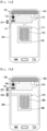
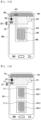
- Figs. 2a , 2b and 2c are conceptual views showing a relative position of the touch sensor panel with respect to the display module in the touch input device according to the embodiment of the present invention. While Figs. 2a to 2c show an LCD panel as a display panel, this is an example outside of the scope of the claims.
- the reference numeral 200 designates the display panel. Also, in Fig. 2 and the description of Fig. 2 , the reference numeral 200 may designate not only the display module but also the display panel.
- the LCD panel may include a liquid crystal layer 250 including a liquid crystal cell, a first glass layer 261 and a second glass layer 262 which are disposed on both sides of the liquid crystal layer 250 and include electrodes, a first polarizer layer 271 formed on a side of the first glass layer 261 in a direction facing the liquid crystal layer 250, and a second polarizer layer 272 formed on a side of the second glass layer 262 in the direction facing the liquid crystal layer 250.
- the LCD panel may further include other configurations for the purpose of performing the displaying function and may be transformed.
- Fig. 2a shows that the touch sensor panel 100 of the touch input device 1000 is disposed outside the display module 200.
- the touch surface of the touch input device 1000 may be the surface of the touch sensor panel 100.
- the top surface of the touch sensor panel 100 is able to function as the touch surface.
- the touch surface of the touch input device 1000 may be the outer surface of the display module 200.
- the bottom surface of the second polarizer layer 272 of the display module 200 is able to function as the touch surface.
- the bottom surface of the display module 200 may be covered with a cover layer (not shown) like glass.
- Figs. 2b and 2c show that the touch sensor panel 100 of the touch input device 1000 is disposed inside the display panel 200.
- the touch sensor panel 100 for detecting the touch position is disposed between the first glass layer 261 and the first polarizer layer 271.
- the touch surface of the touch input device 1000 is the outer surface of the display module 200.
- the top surface or bottom surface of the display module 200 in Fig. 2b may be the touch surface.
- Fig. 2c shows that the touch sensor panel 100 for detecting the touch position is included in the liquid crystal layer 250.
- the touch surface of the touch input device 1000 is the outer surface of the display module 200.
- the top surface or bottom surface of the display module 200 in Fig. 2c may be the touch surface.
- the top surface or bottom surface of the display module 200 which can be the touch surface, may be covered with a cover layer (not shown) like glass.
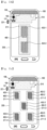
- Fig. 3 is a cross sectional view of the touch input device configured to detect the touch position and touch pressure in accordance with an example of the present invention.
- the touch sensor panel 100 and the pressure detection module 400 which detect the touch position may be attached on the front side of the display module 200, As a result, the display screen of the display module 200 can be protected and the touch detection sensitivity of the touch sensor panel 100 can be improved.
- the pressure detection module 400 may be operated apart from the touch sensor panel 100 which detects the touch position.
- the pressure detection module 400 may be configured to detect only the touch pressure independently of the touch sensor panel 100 which detects the touch position.
- the pressure detection module 400 may be configured to be coupled to the touch sensor panel 100 which detects the touch position and to detect the touch pressure. At least one of the drive electrode TX and the receiving electrode RX included in the touch sensor panel 100 which detects the touch position are used to detect the touch pressure.
- Fig. 3 shows that the pressure detection module 400 is coupled to the touch sensor panel 100 and detects the touch pressure.
- the pressure detection module 400 includes a spacer layer 420 which leaves a space between the touch sensor panel 100 and the display module 200.
- the pressure detection module 400 may include a reference potential layer spaced from the touch sensor panel 100 by the spacer layer 420.
- the display module 200 may function as the reference potential layer.
- the reference potential layer may have any potential which causes the change of the capacitance 101 generated between the drive electrode TX and the receiving electrode RX.
- the reference potential layer may be a ground layer having a ground potential.
- the reference potential layer may be the ground layer of the display module 200.
- the reference potential layer may have a parallel plane with the two-dimensional plane of the display module 200.
- the touch sensor panel 100 is disposed apart from the display module 200, i.e., the reference potential layer.
- the spacer layer 420 may be implemented in the form of an air gap between the touch sensor panel 100 and the display module 200.
- a double adhesive tape (DAT) 430 may be used to fix the touch sensor panel 100 and the display module 200.
- DAT double adhesive tape
- the areas the touch sensor panel 100 and the display module 200 are overlapped with each other.
- the touch sensor panel 100 and the display module 200 are adhered to each other by adhering the edge portions of the touch sensor panel 100 and the display module 200 through use of the DAT 430.
- the rest portions of the touch sensor panel 100 and the display module 200 may be spaced apart from each other by a predetermined distance " d ".
- the capacitance (Cm) 101 between the drive electrode TX and the receiving electrode RX is changed. That is, when the touch occurs on the touch sensor panel 100, the mutual capacitance (Cm) 101 may become smaller than a base mutual capacitance. This is because, when the conductive object like a finger approaches close to the touch sensor panel 100, the object functions as the ground GND, and then a fringing capacitance of the mutual capacitance (Cm) 101 is absorbed in the object.
- the base mutual capacitance is the value of the mutual capacitance between the drive electrode TX and the receiving electrode RX when there is no touch on the touch sensor panel 100.
- the touch sensor panel 100 When the object touches the top surface, i.e., the touch surface of the touch sensor panel 100 and a pressure is applied to the top surface, the touch sensor panel 100 is bent.
- the value of the mutual capacitance (Cm) 101 between the drive electrode TX and the receiving electrode RX may be more reduced.
- the bend of the touch sensor panel 100 causes the distance between the touch sensor panel 100 and the reference potential layer to be reduced from “ d " to " d' ", so that the fringing capacitance of the mutual capacitance (Cm) 101 is absorbed in the reference potential layer as well as in the object.
- the change of the mutual capacitance (Cm) 101 is simply caused by only the change of the distance " d-d' " between the touch sensor panel 100 and the reference potential layer.
- the touch input device 1000 is configured to include the touch sensor panel 100 and the pressure detection module 400 on the display module 200, so that not only the touch position but also the touch pressure can be simultaneously detected.
- the pressure detection module 400 as well as the touch sensor panel 100 is disposed on the display module 200, the display properties of the display module is deteriorated. Particularly, when the air gap 420 is included on the display module 200, the visibility and optical transmittance of the display module may be lowered.
- the air gap is not disposed between the display module 200 and the touch sensor panel 100 for detecting the touch position.
- the touch sensor panel 100 and the display module 200 can be completely laminated by means of an adhesive like an optically clear adhesive (OCA).
- OCA optically clear adhesive
- Fig. 4 is a cross sectional view of the touch input device according to an embodiment of the present invention.
- the complete lamination is made by an adhesive between the touch sensor panel 100 and the display module 200 for detecting the touch position.
- the display color clarity, visibility and optical transmittance of the display module 200 which can be recognized through the touch surface of the touch sensor panel 100, can be improved.
- the touch input device 1000 As the touch input device 1000 according to the embodiment of the present invention, the touch sensor panel 100 is laminated and attached on the display module 200 by means of an adhesive.
- the touch input device 1000 according to the embodiment of the present invention may include, as shown in Figs. 2b and 2c , that the touch sensor panel 100 is disposed inside the display module 200. More specifically, while Figs. 4 and 5 show that the touch sensor panel 100 covers the display module 200, the touch input device 1000 which includes the touch sensor panel 100 disposed inside the display module 200 and includes the display module 200 covered with a cover layer like glass may be used as the embodiment of the present invention.
- the touch input device 1000 may include an electronic device including the touch screen, for example, a cell phone, a personal data assistant (PDA), a smart phone, a tablet personal computer, an MP3 player, a laptop computer, etc.
- PDA personal data assistant
- a smart phone for example, a cell phone, a personal data assistant (PDA), a smart phone, a tablet personal computer, an MP3 player, a laptop computer, etc.
- a substrate 300 together with an outermost cover 320 of the touch input device 1000, functions as, for example, a housing which surrounds a mounting space 310, etc., where the circuit board and/or battery for operation of the touch input device 1000 are placed.
- the circuit board for operation of the touch input device 1000 may be a main board.
- a central processing unit (CPU), an application processor (AP) or the like may be mounted on the circuit board. Due to the substrate 300, the display module 200 is separated from the circuit board and/or battery for operation of the touch input device 1000. Due to the substrate 300, electrical noise generated from the display module 200 can be blocked.
- the touch sensor panel 100 or front cover layer of the touch input device 1000 may be formed wider than the display module 200, the substrate 300, and the mounting space 310.
- the cover 320 is formed such that the cover 320, together with the touch sensor panel 100, surrounds the display module 200, the substrate 300, and the circuit board.
- the touch input device 1000 may detect the touch position through the touch sensor panel 100 and may detect the touch pressure by disposing the pressure detection module 400 between the display module 200 and the substrate 300.
- the touch sensor panel 100 may be disposed inside or outside the display module 200.
- the pressure detection module 400 is formed to include, for example, the spacer layer 420 consisting of the air gap. This will be described in detail with reference to Figs. 5 to 7b .
- the spacer layer 420 may be made of an impact absorbing material in accordance with the embodiment.
- the spacer layer 420 may be filled with a dielectric material in accordance with the embodiment.
- Fig. 5 is a perspective view of the touch input device according to the embodiment of the present invention.
- the pressure detection module 400 includes the spacer layer 420 which leaves a space between the display module 200 and the substrate 300 and includes electrodes 450 and 460 disposed within the spacer layer 420.
- the electrodes 450 and 460 for detecting the pressure are designated as pressure electrodes 450 and 460.
- the pressure electrodes 450 and 460 may be made of an opaque material as well as a transparent material.
- the adhesive tape 440 with a predetermined thickness is formed along the border of the upper portion of the substrate 300 in order to maintain the spacer layer 420. While Fig. 5 shows the adhesive tape 440 is formed on the entire border (e.g., four sides of the quadrangle) of the substrate 300, the adhesive tape 440 may be formed only on at least some (e.g., three sides of the quadrangle) of the border of the substrate 300. According to the embodiment, the adhesive tape 440 may be formed on the top surface of the substrate 300 or on the bottom surface of the display module 200.
- the adhesive tape 440 may be a conductive tape in order that the substrate 300 and the display module 200 have the same electric potential.
- the adhesive tape 440 may be a double adhesive tape.
- the adhesive tape 440 may be made of an inelastic material.
- the display module 200 when a pressure is applied to the display module 200, the display module 200 is bent. Therefore, the magnitude of the touch pressure can be detected even though the adhesive tape 440 is not transformed by the pressure.
- Fig. 6a is a cross sectional view of the touch input device including a pressure electrode pattern according to an example. As shown in Fig. 6a , the pressure electrodes 450 and 460 according to the example may be formed within the spacer layer 420 and on the substrate 300.
- the pressure electrode for detecting the pressure may include the first electrode 450 and the second electrode 460.
- any one of the first electrode 450 and the second electrode 460 may be a drive electrode and the other may be a receiving electrode.
- a drive signal is applied to the drive electrode, and a sensing signal may be obtained through the receiving electrode.
- the mutual capacitance may be generated between the first electrode 450 and the second electrode 460.
- Fig. 6b is a cross sectional view showing a case where a pressure has been applied to the touch input device 1000 shown in Fig. 6a .
- the bottom surface of the display module 200 may have a ground potential so as to block the noise.
- the pressure is applied to the surface of the touch sensor panel 100 by an object 500, the touch sensor panel 100 and the display module 200 is bent.
- the distance " d " between the ground potential surface and the pattern of the pressure electrodes 450 and 460 may be decreased to " d' ".
- the fringing capacitance is absorbed in the bottom surface of the display module 200, so that the mutual capacitance between the first electrode 450 and the second electrode 460 may be reduced. Therefore, the magnitude of the touch pressure can be calculated by obtaining the reduction amount of the mutual capacitance from the sensing signal obtained through the receiving electrode.
- the display module 200 is bent by the touch pressure.
- the display module 200 may be bent in such a manner as to show the biggest transformation at the touch position.
- a position showing the biggest transformation may not match the touch position.
- the display module 200 may be shown to be bent at least at the touch position.
- the touch position approaches close to the border, edge, etc., of the display module 200
- the most bent position of the display module 200 may not match the touch position, however, the display module 200 may be shown to be bent at least at the touch position.
- the top surface of the substrate 300 may also have the ground potential in order to block the noise. Therefore, in order to prevent a short-circuit from occurring between the substrate 300 and the pressure electrodes 450 and 460, the pressure electrodes 450 and 460 may be formed on an insulation layer 470.
- Fig. 8 shows an attachment structure of the pressure electrode according embodiments and examples of the present invention. Referring to Fig. 8(a) , the first insulation layer 470 is positioned on the substrate 300, and then the pressure electrodes 450 and 460 are formed. Also, according to the embodiment, the first insulation layer 470 on which the pressure electrodes 450 and 460 have been formed may be attached on the substrate 300. Also, the pressure electrode according to the embodiment may be formed by positioning a mask, which has a through-hole corresponding to the pressure electrode pattern, on the substrate 300 or on the first insulation layer 470 positioned on the substrate 300, and then by spraying a conductive material.
- the pressure electrodes 450 and 460 may be covered with an additional second insulation layer 471 in order to prevent a short-circuit from occurring between the display module 200 and the pressure electrodes 450 and 460 positioned on the substrate 300. Also, the pressure electrodes 450 and 460 formed on the first insulation layer 470 are covered with the additional second insulation layer 471 and then are integrally attached on the substrate 300, so that the pressure detection module 400 is formed.
- the pressure electrodes 450 and 460 attachment structure and method which have been described with reference to (a) of Fig. 8 , may be applied to the attachment of the pressure electrodes 450 and 460 to the display module 200.
- the attachment of the pressure electrodes 450 and 460 to the display module 200 will be described in more detail with reference to Fig. 6c .
- the substrate 300 or the display module 200 on which the pressure electrodes 450 and 460 are attached may not have the ground potential or may have a weak ground potential.
- the touch input device 1000 according to the embodiment of the present may further include a ground electrode (not shown) between the first insulation layer 470 and either the substrate 300 or the display module 200.
- another insulation layer (not shown) may be included between the ground electrode and either the substrate 300 or the display module 200.
- the ground electrode (not shown) is able to prevent the size of the capacitance generated between the first electrode 450 and the second electrode 460, which are pressure electrodes, from increasing excessively.
- Fig. 6c is a cross sectional view of the touch input device including a pressure electrode according to an embodiment of the present invention. While an example shows that the pressure electrodes 450 and 460 are formed on the substrate 300, the pressure electrodes 450 and 460 are formed on the bottom surface of the display module 200. Here, the substrate 300 may have the ground potential. Therefore, the distance " d " between the substrate 300 and the pressure electrodes 450 and 460 is reduced by touching the touch surface of the touch sensor panel 100. Consequently, this may cause the change of the mutual capacitance between the first electrode 450 and the second electrode 460.
- Fig. 6d shows a pattern of the pressure electrode according to an example.
- Fig. 6d shows that the first electrode 450 and the second electrode 460 are formed on the substrate 300.
- the capacitance between the first electrode 450 and the second electrode 460 may be changed depending on the distance between the bottom surface of the display module 200 and the pressure electrodes 450 and 460.
- Fig. 6e shows a pattern of the pressure electrode according to the embodiment of the present invention.
- Fig. 6e shows that the pressure electrode patterns 450 and 460 have been formed on the bottom surface of the display module 200.
- Figs. 6f to 6g show patterns of the pressure electrodes 450 and 460 which can be applied to the embodiment of the present invention.
- the magnitude of the touch pressure is detected as the mutual capacitance between the first electrode 450 and the second electrode 460 is changed, it is necessary to form the patterns of the first electrode 450 and the second electrode 460 so as to generate the range of the capacitance required to improve the detection accuracy.
- the pattern can be designed by adjusting the size of the facing area, facing length and facing shape of the first electrode 450 and the second electrode 460 in accordance with the range of the necessary capacitance.
- Figs. 6f and 6g show that the first electrode 450 and the second electrode 460 are formed in the same layer, and show that the pressure electrode is formed such that the facing length of the first electrode 450 and the second electrode 460 becomes relatively longer.
- the embodiments show that the first electrode 450 and the second electrode 460 are formed in the same layer. However, it can be considered that the first electrode 450 and the second electrode 460 are formed in different layers in accordance with the embodiment. It is shown in (b) of Fig. 8 that an attachment structure in which the first electrode 450 and the second electrode 460 are formed in different layers. As shown in (b) of Fig.8 , the first electrode 450 may be formed on the first insulation layer 470, and the second electrode 460 may be formed on the second insulation layer 471 positioned on the first electrode 450. According to the embodiment, the second electrode 460 may be covered with a third insulation layer 472.
- first electrode 450 and the second electrode 460 are disposed in different layers, they can be implemented so as to overlap each other.
- the first electrode 450 and the second electrode 460 may be formed similarly to the pattern of the drive electrode TX and receiving electrode RX which are arranged in the form of M ⁇ N array and are included in the touch sensor panel 100 described with reference to Fig. 1 .
- M and N may be natural numbers greater than 1.
- the examples shows that the touch pressure is detected from the change of the mutual capacitance between the first electrode 450 and the second electrode 460.
- the pressure electrodes 450 and 460 may be configured to include only any one of the first electrode 450 and the second electrode 460. In this case, it is possible to detect the magnitude of the touch pressure by detecting the change of the capacitance between the one pressure electrode and the ground layer (either the display module 200 or the substrate 300).
- the pressure electrode may be configured to include only the first electrode 450.
- the magnitude of the touch pressure can be detected by the change of the capacitance between the first electrode 450 and the display module 200, which is caused by the distance change between the display module 200 and the first electrode 450. Since the distance " d " is reduced with the increase of the touch pressure, the capacitance between the display module 200 and the first electrode 450 may be increased with the increase of the touch pressure.
- the pressure electrode should not necessary have a comb teeth shape or a trident shape, which is required to improve the detection accuracy of the mutual capacitance change amount.
- the pressure electrode may have, as shown in Fig. 7b , a plate shape (e.g., quadrangular plate).
- an attachment structure in which the pressure electrode is formed to include only the first electrode 450 may include only the first electrode 450.
- the first electrode 450 may be formed on the first insulation layer 470 positioned on the substrate 300 or display module 200. Also, according to the embodiment, the first electrode 450 may be covered with the second insulation layer 471.
- Fig. 7a is a cross sectional view of the touch input device including the pressure electrode according to an example.
- the pressure electrodes 450 and 460 according to the embodiment may be formed within the spacer layer 420 and on the top surface of the substrate 300 and on the bottom surface of the display module 200.
- the pressure electrode pattern for detecting the pressure may include the first electrode 450 and the second electrode 460.
- any one of the first electrode 450 and the second electrode 460 may be formed on the substrate 300, and the other may be formed on the bottom surface of the display module 200.
- Fig. 7a shows that the first electrode 450 is formed on the substrate 300, and the second electrode 460 is formed on the bottom surface of the display module 200.
- the touch sensor panel 100 and the display module 200 When the pressure is applied to the surface of the touch sensor panel 100 by the object 500, the touch sensor panel 100 and the display module 200 is bent. As a result, the distance " d " between the first electrode 450 and the second electrode 460 may be reduced. In this case, the mutual capacitance between the first electrode 450 and the second electrode 460 may be increased with the reduction of the distance " d ". Therefore, the magnitude of the touch pressure can be calculated by obtaining the increase amount of the mutual capacitance from the sensing signal obtained through the receiving electrode.
- Fig. 7b shows a pattern of the pressure electrode according to the embodiment of the present invention.
- Fig. 7b shows that the first electrode 450 is formed on the top surface of the substrate 300 and the second electrode 460 is formed on the bottom surface of the display module 200.
- the pressure electrodes 450 and 460 since the pressure electrodes 450 and 460 are formed in different layers, the pressure electrodes 450 and 460 should not necessarily have a comb teeth shape or a trident shape unlike the previous embodiments and examples.
- the pressure electrodes 450 and 460 may have a plate shape (e.g., quadrangular plate).
- the first electrode 450 may be positioned on the first insulation layer 470-2 formed on the substrate 300 and may be covered with the second insulation layer 471-2.
- the second electrode 460 may be positioned on the first insulation layer 470-1 formed on the bottom surface of the display module 200 and may be covered with the second insulation layer 471-1.
- a ground electrode may be further included between the first insulation layers 470, 470-1, and 470-2 in (a) to (d) of Fig. 8 .
- an additional insulation layer may be further included between the ground electrode (not shown) and either the substrate 300 or the display module 200 on which the pressure electrodes 450 and 460 are attached.
- the touch input device 1000 senses the capacitance change occurring in the pressure electrodes 450 and 460. Therefore, it is necessary for the drive signal to be applied to the drive electrode out of the first and second electrodes 450 and 460, and it is required to detect the touch pressure by the capacitance change amount by obtaining the sensing signal from the receiving electrode. According to the embodiment, it is possible to additionally include the touch sensing IC for the operation of the pressure detection module 400. In this case, the touch input device repeatedly has a configuration similar to the configuration of Fig. 1 including the drive unit 120, sensing unit 110, and controller 130, so that the area and volume of the touch input device 1000 increase.
- the pressure detection module 400 applies the drive signal for the operation of the touch sensor panel 100 through the touch detection device and receives the sensing signal, so that the touch pressure can be detected.
- the first electrode 450 is the drive electrode and the second electrode 460 is the receiving electrode.
- the drive signal may be applied to the first electrode 450 from the drive unit 120, and the second electrode 460 may transmit the sensing signal to the sensing unit 110.
- the controller 130 may perform the scanning of the touch sensor panel 100, and simultaneously perform the scanning of the pressure detection module 400, or the controller 130 performs the time-sharing, and then may generate a control signal such that the scanning of the touch sensor panel 100 is performed in a first time interval and the scanning of the pressure detection module 400 is performed in a second time interval different from the first time interval.
- the first electrode 450 and the second electrode 460 should be electrically connected to the drive unit 120 and/or the sensing unit 110.
- the touch detection device for the touch sensor panel 100 corresponds to the touch sensing IC 150 and is formed on one end of the touch sensor panel 100 or on the same plane with the touch sensor panel 100.
- the pattern of the pressure electrodes 450 and 460 may be electrically connected to the touch detection device of the touch sensor panel 100 by any method.
- the pattern of the pressure electrodes 450 and 460 may be connected to the touch detection device through a connector by using the second PCB 210 included in the display module 200.
- the conductive traces 451 and 461 which electrically extend from the first electrode 450 and the second electrode 460 respectively may be electrically connected to the touch sensing IC 150 through the second PCB 210, etc.
- Figs. 9a and 9b show an attachment method of the pressure electrode according the embodiment of the present invention.
- Figs. 9a and 9b show that the pressure electrodes 450 and 460 according to the embodiment of the present invention are attached to the bottom surface of the display module 200.
- Figs. 9a and 9b show the second PCB 210 on which a circuit for the operation of the display panel has been mounted is disposed on a portion of the bottom surface of the display module 200.
- Fig. 9a shows that the pattern of the pressure electrodes 450 and 460 are attached to the bottom surface of the display module 200 such that the first electrode 450 and the second electrode 460 are connected to one end of the second PCB 210 of the display module 200.
- Fig. 9a shows that the first electrode 450 and the second electrode 460 are manufactured on the insulation layer 470.
- the pattern of the pressure electrodes 450 and 460 is formed on the insulation layer 470 and may be attached as an integrated formed sheet on the bottom surface of the display module 200.
- a conductive pattern may be printed on the second PCB 210 in such a manner as to electrically connect the pattern of the pressure electrodes 450 and 460 to a necessary component like the touch sensing IC 150, etc. The detailed description of this will be provided with reference to Figs. 10a to 10c .
- Fig. 9b shows that the pressure electrodes 450 and 460 are integrally formed on the second PCB 210 of the display module 200.
- the second PCB 210 of the display module 200 is manufactured, a certain area is separated from the second PCB 210, and then not only the circuit for the operation of the display panel but also the pattern corresponding to the first electrode 450 and the second electrode 460 can be printed on the area.
- a conductive pattern may be printed on the second PCB 210 in such a manner as to electrically connect the first electrode 450 and the second electrode 460 to a necessary component like the touch sensing IC 150, etc.
- Figs 10a to 10c show how the pressure electrode is connected to the touch sensing IC 150 in accordance with the embodiment of the present invention.
- the touch sensor panel 100 is included outside the display module 200.
- Figs. 10a to 10c show that the touch detection device of the touch sensor panel 100 is integrated in the touch sensing IC 150 mounted on the first PCB 160 for the touch sensor panel 100.
- Fig. 10a shows that the pressure electrodes 450 and 460 attached to the display module 200 are connected to the touch sensing IC 150 through a first connector 121.
- the touch sensing IC 150 is connected to the second PCB 210 for the display module 200 through the first connector 121.
- the second PCB 210 may be electrically connected to the main board through a second connector 221. Therefore, through the first connector 121 and the second connector 221, the touch sensing IC 150 may transmit and receive a signal to and from the CPU or AP for the operation of the touch input device 1000.
- FIG. 10a shows that the first electrode 450 is attached to the display module 200 by the method shown in Fig. 9b
- the first electrode 450 can be attached to the display module 200 by the method shown in Fig. 9a .
- a conductive pattern may be printed on the second PCB 210 in such a manner as to electrically connect the first electrode 450 and the second electrode 460 to the touch sensing IC 150 through the first connector 121.
- Fig. 10b shows that the pressure electrodes 450 and 460 attached to the display module 200 are connected to the touch sensing IC 150 through a third connector 473.
- the pressure electrodes 450 and 460 may be connected to the main board for the operation of the touch input device 1000 through the third connector 473, and in the future, may be connected to the touch sensing IC 150 through the second connector 221 and the first connector 121.
- the pressure electrodes 450 and 460 may be printed on the additional PCB 211 separated from the second PCB 210.
- the pattern of the pressure electrodes 450 and 460 may be formed on the insulation layer 470 and may be connected to the main board through the third connector 473 by extending the conductive trace, etc., from the pressure electrodes 450 and 460.
- Fig. 10c shows that the pattern of the pressure electrodes 450 and 460 are directly connected to the touch sensing IC 150 through a fourth connector 474.
- the pressure electrodes 450 and 460 may be connected to the first PCB 160 through the fourth connector 474.
- a conductive pattern may be printed on the first PCB 160 in such a manner as to electrically connect the fourth connector 474 to the touch sensing IC 150.
- the pressure electrodes 450 and 460 may be connected to the touch sensing IC 150 through the fourth connector 474.
- the pressure electrodes 450 and 460 may be printed on the additional PCB 211 separated from the second PCB 210.
- the second PCB 210 may be insulated from the additional PCB 211 so as not to be short-circuited with each other.
- the pressure electrodes 450 and 460 may be formed on the insulation layer 470 and may be connected to the first PCB 160 through the forth connector 474 by extending the conductive trace, etc., from the pressure electrodes 450 and 460.
- connection method of Figs. 10b and 10c can be applied to the case where the pressure electrodes 450 and 460 are formed on the substrate 300 as well as on the bottom surface of the display module 200.
- Figs. 10a to 10c have been described by assuming that a chip on board (COB) structure in which the touch sensing IC 150 is formed on the first PCB 160.
- COB chip on board
- the present invention can be applied to the chip on board (COB) structure in which the touch sensing IC 150 is mounted on the main board within the mounting space 310 of the touch input device 1000. It will be apparent to those skilled in the art from the descriptions of Figs. 10a to 10c that the connection of the pressure electrodes 450 and 460 through the connector can be also applied to another embodiment.
- the pressure electrodes 450 and 460 that is to say, has described that the first electrode 450 constitutes one channel as the drive electrode and the second electrode 460 constitutes one channel as the receiving electrode.
- the drive electrode and the receiving electrode constitute a plurality of channels respectively, so that a plurality of pressure detection can be made based on the multi-touch.
- Figs. 11a to 11c show that the pressure electrode according to the embodiment of the present invention constitutes the plurality of channels.
- Fig. 11a shows the first electrode 450-1 and 450-2 and the second electrode 460-1 and 460-2 constitute two channels respectively.
- Fig. 11b shows that the first electrode 450 constitutes two channels 450-1 and 450-2 and the second electrode 460 constitutes one channel.
- Fig. 11c shows the first electrode 450-1 to 450-5 and the second electrode 460-1 to 460-5 constitute five channels respectively.
- Figs. 11a to 11c show that the pressure electrode constitutes a single or a plurality of channels.
- the pressure electrode may be comprised of a single or a plurality of channels by a variety of methods. While Figs. 11a to 11c do not show that the pressure electrodes 450 and 460 are electrically connected to the touch sensing IC 150, the pressure electrodes 450 and 460 can be connected to the touch sensing IC 150 by the method shown in Figs. 10a to 10c and other methods.
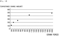
- Fig. 12 is a graph that, when an experiment where the central portion of the touch surface of the touch input device 1000 according to the embodiment of the present invention is pressed by the non-conductive object is performed, represents a capacitance change amount according to a gram force of the object. As shown in Fig. 12 , the greater the force which is applied to the central portion of the touch surface of the touch input device 1000 according to the embodiment of the present invention, the greater the capacitance change amount of the pattern of the pressure electrodes 450 and 460 included in the pressure detection module 400.
- the capacitance type detection module as the pressure detection module 400.
- the spacer layer 420 and the pressure electrodes 450 and 460 are used as the pressure detection module 400, the touch input device 1000 according to the embodiment of the present is able to use any type pressure
- a touch input device which includes a display module and is capable of detecting a magnitude of a touch pressure as well as a touch position on a touch screen.
- a touch input device which includes a display module and is capable of detecting the touch position and the magnitude of the touch pressure without reducing the visibility and optical transmittance of the display module.
Landscapes
- Engineering & Computer Science (AREA)
- Theoretical Computer Science (AREA)
- General Engineering & Computer Science (AREA)
- Physics & Mathematics (AREA)
- General Physics & Mathematics (AREA)
- Human Computer Interaction (AREA)
- Position Input By Displaying (AREA)
- Telephone Set Structure (AREA)
- Chemical & Material Sciences (AREA)
- Crystallography & Structural Chemistry (AREA)
- Computer Hardware Design (AREA)
Applications Claiming Priority (3)
| Application Number | Priority Date | Filing Date | Title |
|---|---|---|---|
| KR1020140098917A KR101681305B1 (ko) | 2014-08-01 | 2014-08-01 | 터치 입력 장치 |
| EP15812868.6A EP3018565B1 (en) | 2014-08-01 | 2015-07-31 | Smart phone |
| PCT/KR2015/008058 WO2016018126A1 (ko) | 2014-08-01 | 2015-07-31 | 스마트폰 |
Related Parent Applications (2)
| Application Number | Title | Priority Date | Filing Date |
|---|---|---|---|
| EP15812868.6A Division EP3018565B1 (en) | 2014-08-01 | 2015-07-31 | Smart phone |
| EP15812868.6A Division-Into EP3018565B1 (en) | 2014-08-01 | 2015-07-31 | Smart phone |
Publications (2)
| Publication Number | Publication Date |
|---|---|
| EP3048514A1 EP3048514A1 (en) | 2016-07-27 |
| EP3048514B1 true EP3048514B1 (en) | 2024-10-09 |
Family
ID=55180644
Family Applications (3)
| Application Number | Title | Priority Date | Filing Date |
|---|---|---|---|
| EP16152697.5A Active EP3048514B1 (en) | 2014-08-01 | 2015-07-31 | Touch input device |
| EP16153159.5A Active EP3059666B1 (en) | 2014-08-01 | 2015-07-31 | Touch input device |
| EP15812868.6A Active EP3018565B1 (en) | 2014-08-01 | 2015-07-31 | Smart phone |
Family Applications After (2)
| Application Number | Title | Priority Date | Filing Date |
|---|---|---|---|
| EP16153159.5A Active EP3059666B1 (en) | 2014-08-01 | 2015-07-31 | Touch input device |
| EP15812868.6A Active EP3018565B1 (en) | 2014-08-01 | 2015-07-31 | Smart phone |
Country Status (6)
| Country | Link |
|---|---|
| US (5) | US10133377B2 (enExample) |
| EP (3) | EP3048514B1 (enExample) |
| JP (5) | JP6145134B2 (enExample) |
| KR (1) | KR101681305B1 (enExample) |
| CN (2) | CN207198825U (enExample) |
| WO (1) | WO2016018126A1 (enExample) |
Families Citing this family (70)
| Publication number | Priority date | Publication date | Assignee | Title |
|---|---|---|---|---|
| DE112013002288T5 (de) | 2012-05-03 | 2015-04-16 | Apple Inc. | Momentkompensierter Biegebalkensensor zur Lastmessung auf einer Biegebalken-gestützten Plattform |
| US9983715B2 (en) | 2012-12-17 | 2018-05-29 | Apple Inc. | Force detection in touch devices using piezoelectric sensors |
| US9952703B2 (en) | 2013-03-15 | 2018-04-24 | Apple Inc. | Force sensing of inputs through strain analysis |
| KR101452302B1 (ko) | 2013-07-29 | 2014-10-22 | 주식회사 하이딥 | 터치 센서 패널 |
| US10007380B2 (en) | 2013-07-29 | 2018-06-26 | Hideep Inc. | Touch input device with edge support member |
| KR101681305B1 (ko) | 2014-08-01 | 2016-12-02 | 주식회사 하이딥 | 터치 입력 장치 |
| US10120478B2 (en) | 2013-10-28 | 2018-11-06 | Apple Inc. | Piezo based force sensing |
| KR101712346B1 (ko) | 2014-09-19 | 2017-03-22 | 주식회사 하이딥 | 터치 입력 장치 |
| AU2015100011B4 (en) | 2014-01-13 | 2015-07-16 | Apple Inc. | Temperature compensating transparent force sensor |
| JP6527343B2 (ja) | 2014-08-01 | 2019-06-05 | 株式会社 ハイディープHiDeep Inc. | タッチ入力装置 |
| JP5845371B1 (ja) | 2014-09-19 | 2016-01-20 | 株式会社 ハイディープ | スマートフォン |
| KR20160068439A (ko) * | 2014-12-05 | 2016-06-15 | 삼성전자주식회사 | 하이브리드 터치 기반 전자 장치 및 그 제어 방법 |
| US9612170B2 (en) | 2015-07-21 | 2017-04-04 | Apple Inc. | Transparent strain sensors in an electronic device |
| KR101583765B1 (ko) | 2015-07-27 | 2016-01-08 | 주식회사 하이딥 | 스마트폰 |
| US10055048B2 (en) | 2015-07-31 | 2018-08-21 | Apple Inc. | Noise adaptive force touch |
| US9874965B2 (en) | 2015-09-11 | 2018-01-23 | Apple Inc. | Transparent strain sensors in an electronic device |
| US9886118B2 (en) | 2015-09-30 | 2018-02-06 | Apple Inc. | Transparent force sensitive structures in an electronic device |
| US10006820B2 (en) | 2016-03-08 | 2018-06-26 | Apple Inc. | Magnetic interference avoidance in resistive sensors |
| JP6297613B2 (ja) * | 2016-03-22 | 2018-03-20 | Nissha株式会社 | 感圧センサ |
| JP6700896B2 (ja) * | 2016-03-25 | 2020-05-27 | 株式会社ジャパンディスプレイ | 検出装置及びタッチ検出機能付き表示装置 |
| WO2017170131A1 (ja) * | 2016-03-28 | 2017-10-05 | シャープ株式会社 | 圧力センサ付表示パネル |
| US10209830B2 (en) * | 2016-03-31 | 2019-02-19 | Apple Inc. | Electronic device having direction-dependent strain elements |
| US10775943B2 (en) * | 2016-04-05 | 2020-09-15 | Hideep Inc. | Pressure sensor, touch input device including same, and pressure detection method using same |
| JP6671461B2 (ja) * | 2016-04-08 | 2020-03-25 | 株式会社 ハイディープHiDeep Inc. | 複数のチャネルを構成する圧力センサ、これを含むタッチ入力装置及びこれを用いた圧力検出方法 |
| KR101963994B1 (ko) | 2016-06-15 | 2019-07-23 | 선전 구딕스 테크놀로지 컴퍼니, 리미티드 | 압력 검출 장치, 방법, 터치 제어 기기 및 전자 단말기 |
| KR102044083B1 (ko) * | 2016-06-16 | 2019-11-12 | 선전 구딕스 테크놀로지 컴퍼니, 리미티드 | 터치 검출 장치 및 검출 방법, 그리고 터치 기기 |
| KR102555596B1 (ko) | 2016-06-21 | 2023-07-17 | 삼성디스플레이 주식회사 | 전자 장치 |
| CN107562237A (zh) * | 2016-07-01 | 2018-01-09 | 南昌欧菲生物识别技术有限公司 | 压力感应触控屏 |
| KR102542992B1 (ko) * | 2016-07-14 | 2023-06-15 | 삼성디스플레이 주식회사 | 터치 센서 및 이를 포함하는 표시 장치 |
| KR102552283B1 (ko) * | 2016-07-15 | 2023-07-10 | 삼성디스플레이 주식회사 | 압력 센서 및 이를 포함하는 표시 장치 |
| KR102531168B1 (ko) | 2016-07-26 | 2023-05-12 | 삼성디스플레이 주식회사 | 표시 장치 |
| KR102562612B1 (ko) | 2016-08-05 | 2023-08-03 | 삼성전자주식회사 | 압력 센서를 구비한 디스플레이를 포함하는 전자 장치 |
| KR102589636B1 (ko) * | 2016-08-05 | 2023-10-17 | 삼성전자주식회사 | 지문 센서를 포함하는 전자 장치 |
| US10133418B2 (en) * | 2016-09-07 | 2018-11-20 | Apple Inc. | Force sensing in an electronic device using a single layer of strain-sensitive structures |
| KR102373566B1 (ko) | 2016-09-23 | 2022-03-14 | 삼성디스플레이 주식회사 | 표시 장치 |
| KR101956295B1 (ko) * | 2016-11-22 | 2019-03-08 | 주식회사 하이딥 | 터치 입력 장치 |
| US11561636B2 (en) * | 2016-11-24 | 2023-01-24 | Hideep Inc. | Touch input device for detecting pressure with display noise compensation |
| KR101908463B1 (ko) * | 2017-02-16 | 2018-10-17 | 주식회사 하이딥 | 터치 입력 장치 |
| DE112018001389T5 (de) * | 2017-03-15 | 2019-11-28 | Mitsubishi Electric Corporation | Touchpanel und Anzeigevorrichtung, die mit einem solchen ausgestattet ist |
| JP6388101B1 (ja) * | 2017-03-15 | 2018-09-12 | 三菱電機株式会社 | タッチパネルおよびタッチパネルを備える表示装置 |
| US11487390B2 (en) | 2017-03-28 | 2022-11-01 | Sony Corporation | Information processing apparatus and control method of information processing apparatus |
| WO2018180845A1 (ja) * | 2017-03-29 | 2018-10-04 | シャープ株式会社 | タッチパネルおよび表示装置 |
| US10444091B2 (en) | 2017-04-11 | 2019-10-15 | Apple Inc. | Row column architecture for strain sensing |
| KR101939280B1 (ko) * | 2017-05-19 | 2019-01-18 | 주식회사 시노펙스 | 정전용량 포스 센서 스위치 |
| US10309846B2 (en) | 2017-07-24 | 2019-06-04 | Apple Inc. | Magnetic field cancellation for strain sensors |
| CN207068439U (zh) * | 2017-08-16 | 2018-03-02 | 京东方科技集团股份有限公司 | 点灯机 |
| KR102405666B1 (ko) * | 2017-08-18 | 2022-06-07 | 삼성전자주식회사 | 터치 감지 신호를 제어하는 전자 장치, 방법 및 저장 매체 |
| CN107608559B (zh) * | 2017-10-16 | 2021-03-02 | 京东方科技集团股份有限公司 | 力感单元及其制备方法、触控面板和触控显示面板 |
| KR102545479B1 (ko) * | 2018-07-31 | 2023-06-20 | 삼성디스플레이 주식회사 | 표시 장치 |
| KR102550324B1 (ko) * | 2018-08-01 | 2023-07-03 | 삼성디스플레이 주식회사 | 표시 장치 |
| KR102626021B1 (ko) * | 2018-08-14 | 2024-01-17 | 삼성디스플레이 주식회사 | 표시 장치 |
| US10782818B2 (en) | 2018-08-29 | 2020-09-22 | Apple Inc. | Load cell array for detection of force input to an electronic device enclosure |
| KR102018155B1 (ko) * | 2018-10-10 | 2019-09-04 | 주식회사 하이딥 | 터치 입력 장치 |
| KR102151986B1 (ko) * | 2018-11-16 | 2020-09-04 | 한국과학기술원 | 터치입력장치 및 터치입력장치 제조 방법 |
| KR102145567B1 (ko) * | 2018-11-29 | 2020-08-18 | 한국과학기술원 | 터치 입력 장치, 터치 입력 장치용 그레이팅 기판, 및 터치 입력 장치용 그레이팅 기판 제조 방법 |
| KR102233459B1 (ko) * | 2019-01-22 | 2021-03-29 | 한국과학기술원 | 터치 입력 장치 및 터치 입력 장치 제조 방법 |
| KR102650383B1 (ko) | 2019-03-26 | 2024-03-25 | 삼성디스플레이 주식회사 | 전자 장치 및 이의 구동 방법 |
| KR102802744B1 (ko) * | 2019-03-28 | 2025-05-02 | 삼성디스플레이 주식회사 | 표시 장치 |
| US11275460B2 (en) * | 2019-04-26 | 2022-03-15 | Samsung Display Co., Ltd. | Display device |
| KR102829293B1 (ko) | 2019-06-14 | 2025-07-04 | 삼성디스플레이 주식회사 | 표시모듈 및 이를 포함하는 표시장치 |
| KR102437876B1 (ko) * | 2019-06-28 | 2022-09-01 | (주)아이테드 | 투명발열모듈을 포함하는 전자장치 |
| KR102234090B1 (ko) * | 2019-06-28 | 2021-03-31 | (주)아이테드 | 투명발열모듈을 포함하는 전자장치 |
| KR102330801B1 (ko) | 2019-12-31 | 2021-11-25 | 한국과학기술원 | 터치 입력 장치 |
| JP7321112B2 (ja) * | 2020-02-10 | 2023-08-04 | 三菱電機株式会社 | タッチパネルおよびこれを備えた表示装置 |
| JP2022035172A (ja) | 2020-08-20 | 2022-03-04 | 株式会社ジャパンディスプレイ | 表示装置、検出装置および時計 |
| CN215406379U (zh) | 2021-06-21 | 2022-01-04 | 上海科勒电子科技有限公司 | 智能马桶遥控器及智能马桶控制系统 |
| US11726597B1 (en) | 2022-05-27 | 2023-08-15 | Microsoft Technology Licensing, Llc | Differential capacitive force sensing |
| US12523552B2 (en) | 2023-05-19 | 2026-01-13 | Microsoft Technology Licensing, Llc | Touchpad force calculation |
| US12099667B1 (en) * | 2023-05-19 | 2024-09-24 | Microsoft Technology Licensing, Llc | Force sensing touchpad |
| WO2025028141A1 (ja) * | 2023-07-28 | 2025-02-06 | 株式会社村田製作所 | センサ及び電子機器 |
Citations (1)
| Publication number | Priority date | Publication date | Assignee | Title |
|---|---|---|---|---|
| US20130234734A1 (en) * | 2012-03-09 | 2013-09-12 | Sony Corporation | Sensor unit, input device, and electronic apparatus |
Family Cites Families (107)
| Publication number | Priority date | Publication date | Assignee | Title |
|---|---|---|---|---|
| BE1007462A3 (nl) * | 1993-08-26 | 1995-07-04 | Philips Electronics Nv | Dataverwerkings inrichting met aanraakscherm en krachtopnemer. |
| JP2000347807A (ja) | 1999-06-08 | 2000-12-15 | Newcom:Kk | 指やペンなどにより入力可能な座標入力装置 |
| US6833943B2 (en) | 2000-03-03 | 2004-12-21 | Sipix Imaging, Inc. | Electrophoretic display and novel process for its manufacture |
| US20020078459A1 (en) | 2000-08-30 | 2002-06-20 | Mckay Brent | Interactive electronic directory service, public information and general content delivery system and method |
| JP2002366304A (ja) * | 2001-06-07 | 2002-12-20 | Alps Electric Co Ltd | 座標入力装置 |
| US7148882B2 (en) | 2003-05-16 | 2006-12-12 | 3M Innovatie Properties Company | Capacitor based force sensor |
| US7924269B2 (en) * | 2005-01-04 | 2011-04-12 | Tpo Displays Corp. | Display devices and methods forming the same |
| US7538760B2 (en) * | 2006-03-30 | 2009-05-26 | Apple Inc. | Force imaging input device and system |
| JP5084176B2 (ja) | 2006-05-31 | 2012-11-28 | 株式会社ブリヂストン | タッチパネル一体型情報表示装置 |
| US8243027B2 (en) * | 2006-06-09 | 2012-08-14 | Apple Inc. | Touch screen liquid crystal display |
| EP3264240A1 (en) | 2006-06-09 | 2018-01-03 | Apple Inc. | Touch screen liquid crystal display |
| US20100033354A1 (en) | 2006-12-15 | 2010-02-11 | Bang & Olufsen A/S | Touch sensitive device |
| US20080202251A1 (en) | 2007-02-27 | 2008-08-28 | Iee International Electronics & Engineering S.A. | Capacitive pressure sensor |
| JP5043641B2 (ja) | 2007-12-28 | 2012-10-10 | キヤノン株式会社 | 入力装置 |
| KR20090076126A (ko) | 2008-01-07 | 2009-07-13 | 엘지전자 주식회사 | 압력 감지용 터치스크린 |
| JP4816668B2 (ja) * | 2008-03-28 | 2011-11-16 | ソニー株式会社 | タッチセンサ付き表示装置 |
| KR20090112118A (ko) * | 2008-04-23 | 2009-10-28 | 엘지이노텍 주식회사 | 표시장치 |
| US7784366B2 (en) * | 2008-07-29 | 2010-08-31 | Motorola, Inc. | Single sided capacitive force sensor for electronic devices |
| KR101025613B1 (ko) | 2008-08-27 | 2011-03-30 | 한국표준과학연구원 | 정전용량 방식의 멀티터치에 따른 접촉위치 및 누름힘 측정용 터치입력구조 |
| KR101065313B1 (ko) | 2008-11-14 | 2011-09-16 | 삼성모바일디스플레이주식회사 | 유기 발광 디스플레이 장치 |
| WO2010074116A1 (ja) | 2008-12-25 | 2010-07-01 | 日本写真印刷株式会社 | 押圧検出機能を有するタッチパネル及び当該タッチパネル用感圧センサ |
| JP5493739B2 (ja) * | 2009-03-19 | 2014-05-14 | ソニー株式会社 | センサ装置及び情報処理装置 |
| US9024907B2 (en) * | 2009-04-03 | 2015-05-05 | Synaptics Incorporated | Input device with capacitive force sensor and method for constructing the same |
| TW201044431A (en) | 2009-06-04 | 2010-12-16 | Ichia Tech Inc | Mechanical keypad with touch pad function |
| JP5164930B2 (ja) | 2009-06-05 | 2013-03-21 | 株式会社ジャパンディスプレイウェスト | タッチパネル、表示パネル、および表示装置 |
| US8248554B2 (en) | 2009-06-19 | 2012-08-21 | Apple Inc. | Edge-lit backlight unit with thin profile |
| CN102334088B (zh) * | 2009-07-29 | 2015-04-15 | 阿尔卑斯电气株式会社 | 操作装置 |
| JP2011119068A (ja) | 2009-12-01 | 2011-06-16 | Nitto Denko Corp | 色素増感型太陽電池用電極および色素増感型太陽電池 |
| US8413529B2 (en) | 2009-08-02 | 2013-04-09 | Steve Carkner | Reusable blood specimen transfer device |
| US8621942B2 (en) | 2009-08-03 | 2014-01-07 | Atmel Corporation | Force sensor with compressible electrode |
| JP2011081578A (ja) | 2009-10-07 | 2011-04-21 | Hitachi Displays Ltd | 表示装置 |
| JP2011086191A (ja) * | 2009-10-16 | 2011-04-28 | Sony Corp | 電子機器 |
| JP5358392B2 (ja) * | 2009-10-21 | 2013-12-04 | アルプス電気株式会社 | 入力処理装置 |
| US9274553B2 (en) * | 2009-10-30 | 2016-03-01 | Synaptics Incorporated | Fingerprint sensor and integratable electronic display |
| GB2475054A (en) * | 2009-11-03 | 2011-05-11 | Sharp Kk | Touch sensing circuits with a voltage dependent capacitor |
| JP5347913B2 (ja) * | 2009-11-06 | 2013-11-20 | ソニー株式会社 | センサ装置、電子機器、及びセンサ装置の製造方法 |
| KR101033154B1 (ko) | 2010-03-11 | 2011-05-11 | 주식회사 디오시스템즈 | 터치 패널 |
| JP5902148B2 (ja) | 2010-03-31 | 2016-04-13 | アベラ ファーマスーティカルズ インコーポレイテッド | 自閉症治療用ジメチルスルホキシド(dmso)製剤 |
| TWI420364B (zh) * | 2010-05-03 | 2013-12-21 | Htc Corp | 觸控式電子裝置及其相關組裝方法 |
| JP2011237489A (ja) * | 2010-05-06 | 2011-11-24 | Toshiba Mobile Display Co Ltd | 有機el表示装置 |
| JP2011248439A (ja) * | 2010-05-24 | 2011-12-08 | Omron Corp | 静電容量式入力装置 |
| JP5598104B2 (ja) * | 2010-06-10 | 2014-10-01 | ソニー株式会社 | 情報処理装置、情報処理方法及びコンピュータプログラム |
| US8599165B2 (en) | 2010-08-16 | 2013-12-03 | Perceptive Pixel Inc. | Force and true capacitive touch measurement techniques for capacitive touch sensors |
| KR20120019543A (ko) | 2010-08-26 | 2012-03-07 | 삼성전자주식회사 | 온-셀 tsp 표시장치 |
| JP5625669B2 (ja) * | 2010-09-17 | 2014-11-19 | ソニー株式会社 | センサ装置および情報処理装置 |
| JP2012084025A (ja) * | 2010-10-14 | 2012-04-26 | Hitachi Displays Ltd | タッチパネル付き表示装置 |
| KR20120044501A (ko) | 2010-10-28 | 2012-05-08 | 삼성모바일디스플레이주식회사 | 터치 스크린 패널을 구비한 표시 장치 및 그 제조 방법 |
| US20120113361A1 (en) | 2010-11-10 | 2012-05-10 | Tpk Touch Solutions Inc. | Optical Level Composite Pressure-Sensitive Adhesive and an Apparatus Therewith |
| KR101190510B1 (ko) | 2010-11-18 | 2012-10-16 | 안철흥 | 패턴화된 투명 도전 필름의 제조 방법 |
| KR101689331B1 (ko) | 2010-11-23 | 2016-12-26 | 삼성디스플레이 주식회사 | 터치 스크린 패널 일체형 평판표시장치 |
| JP2012145497A (ja) | 2011-01-13 | 2012-08-02 | Fanuc Ltd | 静電容量式力センサ |
| JP2012235224A (ja) * | 2011-04-28 | 2012-11-29 | Jvc Kenwood Corp | 電子機器 |
| KR20120139518A (ko) | 2011-06-16 | 2012-12-27 | 솔렌시스 주식회사 | 정전 용량 및 압력 센싱이 가능한 하이브리드 터치 패널 |
| US9678586B2 (en) * | 2011-06-20 | 2017-06-13 | Synaptics Incorporated | Touch and display device having an integrated sensor controller |
| US20130016059A1 (en) | 2011-07-12 | 2013-01-17 | Research In Motion Limited | Electronic device and method of controlling a touch-sensitive display |
| US20130016060A1 (en) | 2011-07-12 | 2013-01-17 | Research In Motion Limited | Electronic device and method of controlling a touch-sensitive display |
| US20130018489A1 (en) * | 2011-07-14 | 2013-01-17 | Grunthaner Martin Paul | Combined force and proximity sensing |
| JP5400904B2 (ja) * | 2011-07-15 | 2014-01-29 | アルプス電気株式会社 | タッチパネル一体型表示装置の製造方法 |
| US8698769B2 (en) | 2011-08-01 | 2014-04-15 | Sharp Kabushiki Kaisha | Dual mode capacitive touch panel |
| US9470941B2 (en) * | 2011-08-19 | 2016-10-18 | Apple Inc. | In-cell or on-cell touch sensor with color filter on array |
| US10261370B2 (en) * | 2011-10-05 | 2019-04-16 | Apple Inc. | Displays with minimized border regions having an apertured TFT layer for signal conductors |
| JP5667960B2 (ja) | 2011-10-14 | 2015-02-12 | 株式会社ジャパンディスプレイ | 表示装置、タッチ検出装置、および電子機器 |
| US9857923B2 (en) | 2011-10-27 | 2018-01-02 | Lg Innotek Co., Ltd. | Touch panel including an elastic intermediate layer |
| US9079384B2 (en) * | 2011-11-11 | 2015-07-14 | Apple Inc. | Touch sensor panel having an index matching passivation layer |
| US9001080B2 (en) * | 2011-11-11 | 2015-04-07 | Panasonic Intellectual Property Management Co., Ltd. | Touch-panel device |
| JP5896692B2 (ja) * | 2011-11-16 | 2016-03-30 | 日東電工株式会社 | 入力表示装置 |
| JP6022164B2 (ja) | 2012-01-24 | 2016-11-09 | 株式会社ジャパンディスプレイ | 液晶表示装置 |
| JP2013171369A (ja) * | 2012-02-20 | 2013-09-02 | Panasonic Liquid Crystal Display Co Ltd | エンベディッド型タッチスクリーン |
| KR101871667B1 (ko) * | 2012-03-16 | 2018-06-27 | 엘지디스플레이 주식회사 | 터치스크린 연결용 연성인쇄회로기판 및 이를 이용한 액정표시장치 |
| KR101311235B1 (ko) | 2012-03-22 | 2013-09-25 | 세원텔레텍 주식회사 | 디스플레이의 컬러 필터 일체형 터치 스크린 |
| JP5865851B2 (ja) | 2012-03-23 | 2016-02-17 | 富士フイルム株式会社 | 導電性部材の製造方法、導電性部材、それを用いたタッチパネル |
| US9665214B2 (en) | 2012-03-29 | 2017-05-30 | Synaptics Incorporated | System and methods for determining object information using selectively floated electrodes |
| US9430107B2 (en) | 2012-03-30 | 2016-08-30 | Microchip Technology Incorporated | Determining touch locations and forces thereto on a touch and force sensing surface |
| KR101351350B1 (ko) | 2012-05-14 | 2014-01-15 | (주)넥스디스플레이 | 쿠션 테잎을 포함하는 백라이트 유닛 및 이를 포함하는 lcd 모듈 |
| JP6122253B2 (ja) | 2012-05-22 | 2017-04-26 | 株式会社オプトラン | 静電容量型タッチパネル基板及びその製造方法並びに製造装置 |
| WO2013177322A1 (en) * | 2012-05-22 | 2013-11-28 | Synaptics Incorporated | Force enhanced input device |
| KR101441971B1 (ko) | 2012-05-24 | 2014-09-24 | (주)멜파스 | 전극-윈도우 일체형 터치 스크린 패널 및 그 터치 스크린 패널을 포함한 터치 스크린 디스플레이 장치 |
| WO2013183234A1 (ja) * | 2012-06-06 | 2013-12-12 | パナソニック株式会社 | 透明電極およびその製造方法 |
| WO2013187281A1 (ja) | 2012-06-11 | 2013-12-19 | シャープ株式会社 | 表示装置 |
| JP2015180978A (ja) | 2012-07-27 | 2015-10-15 | シャープ株式会社 | タッチパネルおよび表示装置 |
| TWI477853B (zh) | 2012-08-20 | 2015-03-21 | Chih Chung Lin | 觸控面板及其製造方法 |
| US9182859B2 (en) | 2012-08-29 | 2015-11-10 | Sharp Kabushiki Kaisha | Capacitive touch panel with force sensing |
| KR101452042B1 (ko) | 2012-09-14 | 2014-10-21 | 삼성전기주식회사 | 터치스크린 패널 및 터치스크린 장치 |
| JP5888686B2 (ja) * | 2012-11-26 | 2016-03-22 | 学校法人福岡大学 | 近接・接触センサ |
| JP6035132B2 (ja) * | 2012-12-06 | 2016-11-30 | 株式会社ジャパンディスプレイ | 液晶表示装置 |
| CN103941926B (zh) | 2013-01-18 | 2017-09-01 | 瀚宇彩晶股份有限公司 | 具有触控功能的显示装置 |
| JP5741879B2 (ja) | 2013-01-25 | 2015-07-01 | 凸版印刷株式会社 | カラーフィルタ基板、及び液晶表示装置 |
| KR102037361B1 (ko) | 2013-01-29 | 2019-10-28 | 엘지디스플레이 주식회사 | 터치표시장치 |
| US9195354B2 (en) | 2013-03-12 | 2015-11-24 | Synaptics Incorporated | Device and method for localized force and proximity sensing |
| US9229592B2 (en) * | 2013-03-14 | 2016-01-05 | Synaptics Incorporated | Shear force detection using capacitive sensors |
| JP6079372B2 (ja) | 2013-03-28 | 2017-02-15 | 富士通株式会社 | 検出装置、検出方法および電子機器 |
| CN103226414B (zh) * | 2013-05-02 | 2015-04-08 | 深圳欧菲光科技股份有限公司 | 触摸屏及其制备方法 |
| KR20150011271A (ko) | 2013-07-22 | 2015-01-30 | 엘지이노텍 주식회사 | 터치 윈도우 및 이를 포함하는 디스플레이 |
| KR101681305B1 (ko) | 2014-08-01 | 2016-12-02 | 주식회사 하이딥 | 터치 입력 장치 |
| CN103425347B (zh) * | 2013-08-02 | 2018-01-02 | 敦泰电子有限公司 | 触控显示装置 |
| KR102254761B1 (ko) * | 2013-09-13 | 2021-05-25 | 삼성디스플레이 주식회사 | Cof 패키지, 이를 포함하는 cof 패키지 어레이, 및 표시 장치 |
| KR101506511B1 (ko) | 2013-09-23 | 2015-04-07 | 주식회사 하이딥 | 정전 용량성 위치 및 압력 터치 센싱 장치 |
| US9990087B2 (en) * | 2013-09-28 | 2018-06-05 | Apple Inc. | Compensation for nonlinear variation of gap capacitance with displacement |
| KR102178797B1 (ko) * | 2013-10-04 | 2020-11-16 | 삼성디스플레이 주식회사 | 터치 센서를 포함하는 표시 장치 |
| KR101712346B1 (ko) | 2014-09-19 | 2017-03-22 | 주식회사 하이딥 | 터치 입력 장치 |
| US10691235B2 (en) | 2013-12-13 | 2020-06-23 | Apple Inc. | On-cell touch architecture |
| WO2015106181A1 (en) | 2014-01-13 | 2015-07-16 | Commscope Technologies Llc | Coaxial connector with axial and radial contact between outer conductors |
| AU2015100011B4 (en) | 2014-01-13 | 2015-07-16 | Apple Inc. | Temperature compensating transparent force sensor |
| CA2949221C (en) | 2014-06-23 | 2022-07-26 | Microsoft Technology Licensing, Llc | Capacitive based digitizer sensor |
| JP6527343B2 (ja) | 2014-08-01 | 2019-06-05 | 株式会社 ハイディープHiDeep Inc. | タッチ入力装置 |
| US20160062500A1 (en) | 2014-08-28 | 2016-03-03 | Apple Inc. | Force Sensor with Capacitive Gap Sensing |
| JP5845371B1 (ja) | 2014-09-19 | 2016-01-20 | 株式会社 ハイディープ | スマートフォン |
-
2014
- 2014-08-01 KR KR1020140098917A patent/KR101681305B1/ko active Active
-
2015
- 2015-06-19 JP JP2015124247A patent/JP6145134B2/ja active Active
- 2015-06-22 US US14/745,514 patent/US10133377B2/en active Active
- 2015-07-31 EP EP16152697.5A patent/EP3048514B1/en active Active
- 2015-07-31 CN CN201590000041.9U patent/CN207198825U/zh not_active Expired - Lifetime
- 2015-07-31 CN CN201820269362.4U patent/CN207965848U/zh not_active Expired - Lifetime
- 2015-07-31 EP EP16153159.5A patent/EP3059666B1/en active Active
- 2015-07-31 EP EP15812868.6A patent/EP3018565B1/en active Active
- 2015-07-31 WO PCT/KR2015/008058 patent/WO2016018126A1/ko not_active Ceased
- 2015-11-09 JP JP2015219873A patent/JP6262703B2/ja active Active
-
2016
- 2016-01-11 US US14/992,568 patent/US9454253B2/en active Active
- 2016-01-26 JP JP2016012175A patent/JP2016105304A/ja active Pending
- 2016-01-27 US US15/007,240 patent/US10007371B2/en active Active
- 2016-01-28 JP JP2016014898A patent/JP6163218B2/ja active Active
- 2016-01-29 US US15/009,951 patent/US9547388B2/en active Active
-
2017
- 2017-02-28 JP JP2017036310A patent/JP7198469B2/ja active Active
-
2018
- 2018-10-16 US US16/161,179 patent/US20190050099A1/en not_active Abandoned
Patent Citations (1)
| Publication number | Priority date | Publication date | Assignee | Title |
|---|---|---|---|---|
| US20130234734A1 (en) * | 2012-03-09 | 2013-09-12 | Sony Corporation | Sensor unit, input device, and electronic apparatus |
Also Published As
| Publication number | Publication date |
|---|---|
| US9547388B2 (en) | 2017-01-17 |
| JP6163218B2 (ja) | 2017-07-12 |
| JP2016040711A (ja) | 2016-03-24 |
| CN207198825U (zh) | 2018-04-06 |
| JP2016105306A (ja) | 2016-06-09 |
| EP3048514A1 (en) | 2016-07-27 |
| EP3059666A1 (en) | 2016-08-24 |
| US10133377B2 (en) | 2018-11-20 |
| JP7198469B2 (ja) | 2023-01-04 |
| KR101681305B1 (ko) | 2016-12-02 |
| KR20160015924A (ko) | 2016-02-15 |
| JP2017117490A (ja) | 2017-06-29 |
| US20160035290A1 (en) | 2016-02-04 |
| US20160124570A1 (en) | 2016-05-05 |
| US9454253B2 (en) | 2016-09-27 |
| JP2016105304A (ja) | 2016-06-09 |
| JP6145134B2 (ja) | 2017-06-07 |
| JP6262703B2 (ja) | 2018-01-17 |
| US20190050099A1 (en) | 2019-02-14 |
| EP3018565B1 (en) | 2020-06-10 |
| US10007371B2 (en) | 2018-06-26 |
| CN207965848U (zh) | 2018-10-12 |
| EP3018565A4 (en) | 2017-01-04 |
| WO2016018126A1 (ko) | 2016-02-04 |
| US20160162088A1 (en) | 2016-06-09 |
| JP2016040734A (ja) | 2016-03-24 |
| EP3018565A1 (en) | 2016-05-11 |
| US20160162094A1 (en) | 2016-06-09 |
| EP3059666B1 (en) | 2020-03-25 |
Similar Documents
| Publication | Publication Date | Title |
|---|---|---|
| EP3048514B1 (en) | Touch input device | |
| US10234987B2 (en) | Electrode sheet and touch input device | |
| EP3076274B1 (en) | Mobile phone with touch input display | |
| KR101633923B1 (ko) | 스마트폰 | |
| KR101634315B1 (ko) | 터치 입력 장치 | |
| KR101656755B1 (ko) | 전극시트 및 터치 입력 장치 | |
| KR101763206B1 (ko) | 터치 입력 장치 |
Legal Events
| Date | Code | Title | Description |
|---|---|---|---|
| PUAI | Public reference made under article 153(3) epc to a published international application that has entered the european phase |
Free format text: ORIGINAL CODE: 0009012 |
|
| 17P | Request for examination filed |
Effective date: 20160222 |
|
| AC | Divisional application: reference to earlier application |
Ref document number: 3018565 Country of ref document: EP Kind code of ref document: P |
|
| AK | Designated contracting states |
Kind code of ref document: A1 Designated state(s): AL AT BE BG CH CY CZ DE DK EE ES FI FR GB GR HR HU IE IS IT LI LT LU LV MC MK MT NL NO PL PT RO RS SE SI SK SM TR |
|
| AX | Request for extension of the european patent |
Extension state: BA ME |
|
| RBV | Designated contracting states (corrected) |
Designated state(s): AL AT BE BG CH CY CZ DE DK EE ES FI FR GB GR HR HU IE IS IT LI LT LU LV MC MK MT NL NO PL PT RO RS SE SI SK SM TR |
|
| STAA | Information on the status of an ep patent application or granted ep patent |
Free format text: STATUS: REQUEST FOR EXAMINATION WAS MADE |
|
| R17P | Request for examination filed (corrected) |
Effective date: 20160222 |
|
| STAA | Information on the status of an ep patent application or granted ep patent |
Free format text: STATUS: EXAMINATION IS IN PROGRESS |
|
| 17Q | First examination report despatched |
Effective date: 20210601 |
|
| GRAP | Despatch of communication of intention to grant a patent |
Free format text: ORIGINAL CODE: EPIDOSNIGR1 |
|
| STAA | Information on the status of an ep patent application or granted ep patent |
Free format text: STATUS: GRANT OF PATENT IS INTENDED |
|
| INTG | Intention to grant announced |
Effective date: 20240426 |
|
| GRAS | Grant fee paid |
Free format text: ORIGINAL CODE: EPIDOSNIGR3 |
|
| GRAA | (expected) grant |
Free format text: ORIGINAL CODE: 0009210 |
|
| STAA | Information on the status of an ep patent application or granted ep patent |
Free format text: STATUS: THE PATENT HAS BEEN GRANTED |
|
| AC | Divisional application: reference to earlier application |
Ref document number: 3018565 Country of ref document: EP Kind code of ref document: P |
|
| AK | Designated contracting states |
Kind code of ref document: B1 Designated state(s): AL AT BE BG CH CY CZ DE DK EE ES FI FR GB GR HR HU IE IS IT LI LT LU LV MC MK MT NL NO PL PT RO RS SE SI SK SM TR |
|
| REG | Reference to a national code |
Ref country code: CH Ref legal event code: EP |
|
| REG | Reference to a national code |
Ref country code: DE Ref legal event code: R096 Ref document number: 602015090117 Country of ref document: DE |
|
| REG | Reference to a national code |
Ref country code: IE Ref legal event code: FG4D |
|
| REG | Reference to a national code |
Ref country code: LT Ref legal event code: MG9D |
|
| REG | Reference to a national code |
Ref country code: NL Ref legal event code: MP Effective date: 20241009 |
|
| REG | Reference to a national code |
Ref country code: AT Ref legal event code: MK05 Ref document number: 1731294 Country of ref document: AT Kind code of ref document: T Effective date: 20241009 |
|
| PG25 | Lapsed in a contracting state [announced via postgrant information from national office to epo] |
Ref country code: NL Free format text: LAPSE BECAUSE OF FAILURE TO SUBMIT A TRANSLATION OF THE DESCRIPTION OR TO PAY THE FEE WITHIN THE PRESCRIBED TIME-LIMIT Effective date: 20241009 |
|
| PG25 | Lapsed in a contracting state [announced via postgrant information from national office to epo] |
Ref country code: NL Free format text: LAPSE BECAUSE OF FAILURE TO SUBMIT A TRANSLATION OF THE DESCRIPTION OR TO PAY THE FEE WITHIN THE PRESCRIBED TIME-LIMIT Effective date: 20241009 |
|
| PG25 | Lapsed in a contracting state [announced via postgrant information from national office to epo] |
Ref country code: IS Free format text: LAPSE BECAUSE OF FAILURE TO SUBMIT A TRANSLATION OF THE DESCRIPTION OR TO PAY THE FEE WITHIN THE PRESCRIBED TIME-LIMIT Effective date: 20250209 Ref country code: HR Free format text: LAPSE BECAUSE OF FAILURE TO SUBMIT A TRANSLATION OF THE DESCRIPTION OR TO PAY THE FEE WITHIN THE PRESCRIBED TIME-LIMIT Effective date: 20241009 Ref country code: PT Free format text: LAPSE BECAUSE OF FAILURE TO SUBMIT A TRANSLATION OF THE DESCRIPTION OR TO PAY THE FEE WITHIN THE PRESCRIBED TIME-LIMIT Effective date: 20250210 |
|
| PG25 | Lapsed in a contracting state [announced via postgrant information from national office to epo] |
Ref country code: FI Free format text: LAPSE BECAUSE OF FAILURE TO SUBMIT A TRANSLATION OF THE DESCRIPTION OR TO PAY THE FEE WITHIN THE PRESCRIBED TIME-LIMIT Effective date: 20241009 |
|
| PG25 | Lapsed in a contracting state [announced via postgrant information from national office to epo] |
Ref country code: BG Free format text: LAPSE BECAUSE OF FAILURE TO SUBMIT A TRANSLATION OF THE DESCRIPTION OR TO PAY THE FEE WITHIN THE PRESCRIBED TIME-LIMIT Effective date: 20241009 |
|
| PG25 | Lapsed in a contracting state [announced via postgrant information from national office to epo] |
Ref country code: ES Free format text: LAPSE BECAUSE OF FAILURE TO SUBMIT A TRANSLATION OF THE DESCRIPTION OR TO PAY THE FEE WITHIN THE PRESCRIBED TIME-LIMIT Effective date: 20241009 |
|
| PG25 | Lapsed in a contracting state [announced via postgrant information from national office to epo] |
Ref country code: NO Free format text: LAPSE BECAUSE OF FAILURE TO SUBMIT A TRANSLATION OF THE DESCRIPTION OR TO PAY THE FEE WITHIN THE PRESCRIBED TIME-LIMIT Effective date: 20250109 |
|
| PG25 | Lapsed in a contracting state [announced via postgrant information from national office to epo] |
Ref country code: LV Free format text: LAPSE BECAUSE OF FAILURE TO SUBMIT A TRANSLATION OF THE DESCRIPTION OR TO PAY THE FEE WITHIN THE PRESCRIBED TIME-LIMIT Effective date: 20241009 Ref country code: GR Free format text: LAPSE BECAUSE OF FAILURE TO SUBMIT A TRANSLATION OF THE DESCRIPTION OR TO PAY THE FEE WITHIN THE PRESCRIBED TIME-LIMIT Effective date: 20250110 Ref country code: AT Free format text: LAPSE BECAUSE OF FAILURE TO SUBMIT A TRANSLATION OF THE DESCRIPTION OR TO PAY THE FEE WITHIN THE PRESCRIBED TIME-LIMIT Effective date: 20241009 |
|
| PG25 | Lapsed in a contracting state [announced via postgrant information from national office to epo] |
Ref country code: PL Free format text: LAPSE BECAUSE OF FAILURE TO SUBMIT A TRANSLATION OF THE DESCRIPTION OR TO PAY THE FEE WITHIN THE PRESCRIBED TIME-LIMIT Effective date: 20241009 |
|
| PG25 | Lapsed in a contracting state [announced via postgrant information from national office to epo] |
Ref country code: RS Free format text: LAPSE BECAUSE OF FAILURE TO SUBMIT A TRANSLATION OF THE DESCRIPTION OR TO PAY THE FEE WITHIN THE PRESCRIBED TIME-LIMIT Effective date: 20250109 |
|
| PG25 | Lapsed in a contracting state [announced via postgrant information from national office to epo] |
Ref country code: SM Free format text: LAPSE BECAUSE OF FAILURE TO SUBMIT A TRANSLATION OF THE DESCRIPTION OR TO PAY THE FEE WITHIN THE PRESCRIBED TIME-LIMIT Effective date: 20241009 |
|
| PG25 | Lapsed in a contracting state [announced via postgrant information from national office to epo] |
Ref country code: DK Free format text: LAPSE BECAUSE OF FAILURE TO SUBMIT A TRANSLATION OF THE DESCRIPTION OR TO PAY THE FEE WITHIN THE PRESCRIBED TIME-LIMIT Effective date: 20241009 |
|
| REG | Reference to a national code |
Ref country code: DE Ref legal event code: R097 Ref document number: 602015090117 Country of ref document: DE |
|
| PG25 | Lapsed in a contracting state [announced via postgrant information from national office to epo] |
Ref country code: EE Free format text: LAPSE BECAUSE OF FAILURE TO SUBMIT A TRANSLATION OF THE DESCRIPTION OR TO PAY THE FEE WITHIN THE PRESCRIBED TIME-LIMIT Effective date: 20241009 |
|
| PG25 | Lapsed in a contracting state [announced via postgrant information from national office to epo] |
Ref country code: RO Free format text: LAPSE BECAUSE OF FAILURE TO SUBMIT A TRANSLATION OF THE DESCRIPTION OR TO PAY THE FEE WITHIN THE PRESCRIBED TIME-LIMIT Effective date: 20241009 |
|
| PG25 | Lapsed in a contracting state [announced via postgrant information from national office to epo] |
Ref country code: SK Free format text: LAPSE BECAUSE OF FAILURE TO SUBMIT A TRANSLATION OF THE DESCRIPTION OR TO PAY THE FEE WITHIN THE PRESCRIBED TIME-LIMIT Effective date: 20241009 |
|
| PG25 | Lapsed in a contracting state [announced via postgrant information from national office to epo] |
Ref country code: CZ Free format text: LAPSE BECAUSE OF FAILURE TO SUBMIT A TRANSLATION OF THE DESCRIPTION OR TO PAY THE FEE WITHIN THE PRESCRIBED TIME-LIMIT Effective date: 20241009 |
|
| PG25 | Lapsed in a contracting state [announced via postgrant information from national office to epo] |
Ref country code: IT Free format text: LAPSE BECAUSE OF FAILURE TO SUBMIT A TRANSLATION OF THE DESCRIPTION OR TO PAY THE FEE WITHIN THE PRESCRIBED TIME-LIMIT Effective date: 20241009 |
|
| PLBE | No opposition filed within time limit |
Free format text: ORIGINAL CODE: 0009261 |
|
| STAA | Information on the status of an ep patent application or granted ep patent |
Free format text: STATUS: NO OPPOSITION FILED WITHIN TIME LIMIT |
|
| PG25 | Lapsed in a contracting state [announced via postgrant information from national office to epo] |
Ref country code: SE Free format text: LAPSE BECAUSE OF FAILURE TO SUBMIT A TRANSLATION OF THE DESCRIPTION OR TO PAY THE FEE WITHIN THE PRESCRIBED TIME-LIMIT Effective date: 20241009 |
|
| 26N | No opposition filed |
Effective date: 20250710 |
|
| PGFP | Annual fee paid to national office [announced via postgrant information from national office to epo] |
Ref country code: DE Payment date: 20250919 Year of fee payment: 11 |
|
| PGFP | Annual fee paid to national office [announced via postgrant information from national office to epo] |
Ref country code: GB Payment date: 20250722 Year of fee payment: 11 |
|
| PGFP | Annual fee paid to national office [announced via postgrant information from national office to epo] |
Ref country code: FR Payment date: 20250723 Year of fee payment: 11 |
|
| REG | Reference to a national code |
Ref country code: CH Ref legal event code: H13 Free format text: ST27 STATUS EVENT CODE: U-0-0-H10-H13 (AS PROVIDED BY THE NATIONAL OFFICE) Effective date: 20260224 |
|
| PG25 | Lapsed in a contracting state [announced via postgrant information from national office to epo] |
Ref country code: LU Free format text: LAPSE BECAUSE OF NON-PAYMENT OF DUE FEES Effective date: 20250731 |