EP3017079B2 - Verfahren zur herstellung von tixsi1-xn schichten - Google Patents
Verfahren zur herstellung von tixsi1-xn schichten Download PDFInfo
- Publication number
- EP3017079B2 EP3017079B2 EP14737148.8A EP14737148A EP3017079B2 EP 3017079 B2 EP3017079 B2 EP 3017079B2 EP 14737148 A EP14737148 A EP 14737148A EP 3017079 B2 EP3017079 B2 EP 3017079B2
- Authority
- EP
- European Patent Office
- Prior art keywords
- layer
- coating
- workpiece
- sputtering
- target
- Prior art date
- Legal status (The legal status is an assumption and is not a legal conclusion. Google has not performed a legal analysis and makes no representation as to the accuracy of the status listed.)
- Active
Links
Images
Classifications
-
- C—CHEMISTRY; METALLURGY
- C23—COATING METALLIC MATERIAL; COATING MATERIAL WITH METALLIC MATERIAL; CHEMICAL SURFACE TREATMENT; DIFFUSION TREATMENT OF METALLIC MATERIAL; COATING BY VACUUM EVAPORATION, BY SPUTTERING, BY ION IMPLANTATION OR BY CHEMICAL VAPOUR DEPOSITION, IN GENERAL; INHIBITING CORROSION OF METALLIC MATERIAL OR INCRUSTATION IN GENERAL
- C23C—COATING METALLIC MATERIAL; COATING MATERIAL WITH METALLIC MATERIAL; SURFACE TREATMENT OF METALLIC MATERIAL BY DIFFUSION INTO THE SURFACE, BY CHEMICAL CONVERSION OR SUBSTITUTION; COATING BY VACUUM EVAPORATION, BY SPUTTERING, BY ION IMPLANTATION OR BY CHEMICAL VAPOUR DEPOSITION, IN GENERAL
- C23C14/00—Coating by vacuum evaporation, by sputtering or by ion implantation of the coating forming material
- C23C14/02—Pretreatment of the material to be coated
- C23C14/027—Graded interfaces
-
- C—CHEMISTRY; METALLURGY
- C23—COATING METALLIC MATERIAL; COATING MATERIAL WITH METALLIC MATERIAL; CHEMICAL SURFACE TREATMENT; DIFFUSION TREATMENT OF METALLIC MATERIAL; COATING BY VACUUM EVAPORATION, BY SPUTTERING, BY ION IMPLANTATION OR BY CHEMICAL VAPOUR DEPOSITION, IN GENERAL; INHIBITING CORROSION OF METALLIC MATERIAL OR INCRUSTATION IN GENERAL
- C23C—COATING METALLIC MATERIAL; COATING MATERIAL WITH METALLIC MATERIAL; SURFACE TREATMENT OF METALLIC MATERIAL BY DIFFUSION INTO THE SURFACE, BY CHEMICAL CONVERSION OR SUBSTITUTION; COATING BY VACUUM EVAPORATION, BY SPUTTERING, BY ION IMPLANTATION OR BY CHEMICAL VAPOUR DEPOSITION, IN GENERAL
- C23C14/00—Coating by vacuum evaporation, by sputtering or by ion implantation of the coating forming material
- C23C14/22—Coating by vacuum evaporation, by sputtering or by ion implantation of the coating forming material characterised by the process of coating
- C23C14/34—Sputtering
- C23C14/35—Sputtering by application of a magnetic field, e.g. magnetron sputtering
-
- B—PERFORMING OPERATIONS; TRANSPORTING
- B23—MACHINE TOOLS; METAL-WORKING NOT OTHERWISE PROVIDED FOR
- B23B—TURNING; BORING
- B23B27/00—Tools for turning or boring machines; Tools of a similar kind in general; Accessories therefor
- B23B27/14—Cutting tools of which the bits or tips or cutting inserts are of special material
-
- C—CHEMISTRY; METALLURGY
- C23—COATING METALLIC MATERIAL; COATING MATERIAL WITH METALLIC MATERIAL; CHEMICAL SURFACE TREATMENT; DIFFUSION TREATMENT OF METALLIC MATERIAL; COATING BY VACUUM EVAPORATION, BY SPUTTERING, BY ION IMPLANTATION OR BY CHEMICAL VAPOUR DEPOSITION, IN GENERAL; INHIBITING CORROSION OF METALLIC MATERIAL OR INCRUSTATION IN GENERAL
- C23C—COATING METALLIC MATERIAL; COATING MATERIAL WITH METALLIC MATERIAL; SURFACE TREATMENT OF METALLIC MATERIAL BY DIFFUSION INTO THE SURFACE, BY CHEMICAL CONVERSION OR SUBSTITUTION; COATING BY VACUUM EVAPORATION, BY SPUTTERING, BY ION IMPLANTATION OR BY CHEMICAL VAPOUR DEPOSITION, IN GENERAL
- C23C14/00—Coating by vacuum evaporation, by sputtering or by ion implantation of the coating forming material
- C23C14/06—Coating by vacuum evaporation, by sputtering or by ion implantation of the coating forming material characterised by the coating material
- C23C14/0641—Nitrides
-
- C—CHEMISTRY; METALLURGY
- C23—COATING METALLIC MATERIAL; COATING MATERIAL WITH METALLIC MATERIAL; CHEMICAL SURFACE TREATMENT; DIFFUSION TREATMENT OF METALLIC MATERIAL; COATING BY VACUUM EVAPORATION, BY SPUTTERING, BY ION IMPLANTATION OR BY CHEMICAL VAPOUR DEPOSITION, IN GENERAL; INHIBITING CORROSION OF METALLIC MATERIAL OR INCRUSTATION IN GENERAL
- C23C—COATING METALLIC MATERIAL; COATING MATERIAL WITH METALLIC MATERIAL; SURFACE TREATMENT OF METALLIC MATERIAL BY DIFFUSION INTO THE SURFACE, BY CHEMICAL CONVERSION OR SUBSTITUTION; COATING BY VACUUM EVAPORATION, BY SPUTTERING, BY ION IMPLANTATION OR BY CHEMICAL VAPOUR DEPOSITION, IN GENERAL
- C23C14/00—Coating by vacuum evaporation, by sputtering or by ion implantation of the coating forming material
- C23C14/06—Coating by vacuum evaporation, by sputtering or by ion implantation of the coating forming material characterised by the coating material
- C23C14/0682—Silicides
-
- C—CHEMISTRY; METALLURGY
- C23—COATING METALLIC MATERIAL; COATING MATERIAL WITH METALLIC MATERIAL; CHEMICAL SURFACE TREATMENT; DIFFUSION TREATMENT OF METALLIC MATERIAL; COATING BY VACUUM EVAPORATION, BY SPUTTERING, BY ION IMPLANTATION OR BY CHEMICAL VAPOUR DEPOSITION, IN GENERAL; INHIBITING CORROSION OF METALLIC MATERIAL OR INCRUSTATION IN GENERAL
- C23C—COATING METALLIC MATERIAL; COATING MATERIAL WITH METALLIC MATERIAL; SURFACE TREATMENT OF METALLIC MATERIAL BY DIFFUSION INTO THE SURFACE, BY CHEMICAL CONVERSION OR SUBSTITUTION; COATING BY VACUUM EVAPORATION, BY SPUTTERING, BY ION IMPLANTATION OR BY CHEMICAL VAPOUR DEPOSITION, IN GENERAL
- C23C14/00—Coating by vacuum evaporation, by sputtering or by ion implantation of the coating forming material
- C23C14/22—Coating by vacuum evaporation, by sputtering or by ion implantation of the coating forming material characterised by the process of coating
- C23C14/34—Sputtering
- C23C14/3407—Cathode assembly for sputtering apparatus, e.g. Target
-
- C—CHEMISTRY; METALLURGY
- C23—COATING METALLIC MATERIAL; COATING MATERIAL WITH METALLIC MATERIAL; CHEMICAL SURFACE TREATMENT; DIFFUSION TREATMENT OF METALLIC MATERIAL; COATING BY VACUUM EVAPORATION, BY SPUTTERING, BY ION IMPLANTATION OR BY CHEMICAL VAPOUR DEPOSITION, IN GENERAL; INHIBITING CORROSION OF METALLIC MATERIAL OR INCRUSTATION IN GENERAL
- C23C—COATING METALLIC MATERIAL; COATING MATERIAL WITH METALLIC MATERIAL; SURFACE TREATMENT OF METALLIC MATERIAL BY DIFFUSION INTO THE SURFACE, BY CHEMICAL CONVERSION OR SUBSTITUTION; COATING BY VACUUM EVAPORATION, BY SPUTTERING, BY ION IMPLANTATION OR BY CHEMICAL VAPOUR DEPOSITION, IN GENERAL
- C23C14/00—Coating by vacuum evaporation, by sputtering or by ion implantation of the coating forming material
- C23C14/22—Coating by vacuum evaporation, by sputtering or by ion implantation of the coating forming material characterised by the process of coating
- C23C14/34—Sputtering
- C23C14/3485—Sputtering using pulsed power to the target
-
- C—CHEMISTRY; METALLURGY
- C23—COATING METALLIC MATERIAL; COATING MATERIAL WITH METALLIC MATERIAL; CHEMICAL SURFACE TREATMENT; DIFFUSION TREATMENT OF METALLIC MATERIAL; COATING BY VACUUM EVAPORATION, BY SPUTTERING, BY ION IMPLANTATION OR BY CHEMICAL VAPOUR DEPOSITION, IN GENERAL; INHIBITING CORROSION OF METALLIC MATERIAL OR INCRUSTATION IN GENERAL
- C23C—COATING METALLIC MATERIAL; COATING MATERIAL WITH METALLIC MATERIAL; SURFACE TREATMENT OF METALLIC MATERIAL BY DIFFUSION INTO THE SURFACE, BY CHEMICAL CONVERSION OR SUBSTITUTION; COATING BY VACUUM EVAPORATION, BY SPUTTERING, BY ION IMPLANTATION OR BY CHEMICAL VAPOUR DEPOSITION, IN GENERAL
- C23C14/00—Coating by vacuum evaporation, by sputtering or by ion implantation of the coating forming material
- C23C14/22—Coating by vacuum evaporation, by sputtering or by ion implantation of the coating forming material characterised by the process of coating
- C23C14/34—Sputtering
- C23C14/35—Sputtering by application of a magnetic field, e.g. magnetron sputtering
- C23C14/352—Sputtering by application of a magnetic field, e.g. magnetron sputtering using more than one target
Definitions
- the present invention relates to a coating method.
- Silicon is a chemical element that is sometimes used in connection with hard material layers to increase the layer stress. If the layer tension increases, this usually leads to a greater hardness of the layer. This is also used, for example, in connection with titanium nitride. This results in layers which can be chemically described by the structural formula Ti x Si 1-x N, where x is the concentration of Ti expressed in at% if only the metallic elements are taken into account. With this notation, the atomic concentrations given in percent add up to 100%.
- Such layers can be produced in a very hard form using what is known as cathodic spark evaporation.
- a spark is ignited between a target that supplies the metallic elements, which is used as a cathode, and an anode, via which a high-density electron current is drawn out of the target surface. Due to the very localized very high current density on the target surface, the target surface is locally heated strongly and the material evaporates in ionized form.
- the material vaporized and ionized in this way is then accelerated onto the substrates with the aid of a negative voltage applied to the substrates. If a reactive gas is additionally admitted into the coating chamber, the evaporated ions combine with the reactive gas and form a corresponding layer on the substrate surface.
- HiPIMS High Power Impulse Magnetron Sputtering
- a pulse generator is therefore required as a power source for the HiPIMS process. This pulse generator must be able to deliver very high power pulses, which are, however, very short.
- the pulse generators available today show little flexibility in terms of pulse height and / or pulse duration, for example. Ideally, a square pulse should be emitted. In most cases, however, the power output within a pulse is strongly time-dependent, which has a direct influence on the layer properties, such as hardness, adhesion, internal stress, etc. In addition, the coating rate is negatively influenced by the deviation from the rectangular profile.
- the layers are produced by means of a sputtering process in which there is a constantly high output of the power source.
- Several sputtering cathodes are used here.
- no pulse generator is used, but only a first sputter cathode is initially charged with the full power of the power source and thus with a high power density.
- a second sputtering cathode is then connected to the outputs of the power source. Little happens at first because the impedance of the second sputter cathode to it Time is much higher than the impedance of the first sputtering cathode.
- the power source is typically in the order of 60 kW.
- Typical outputs to which the sputter cathodes are exposed on average over time are of the order of magnitude of 8kW.
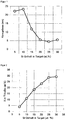
- the inventors have now completely surprisingly found that if such a method is operated with TiSi targets which contain a silicon content greater than or equal to 15 at%, it is possible to produce reproducible nanocrystalline layers with very good mechanical properties. It is particularly interesting that from a Si concentration in the target of 15at% the nanocrystals have an average grain size of less than 15 nm, as in FIG Figure 1 shown. That the concentration ratios in the target used for the coating are almost directly reflected in the coated layer is shown in Figure 2 shown. It should be noted at this point that as soon as a target with a certain Si concentration has been selected, the grain size can be finely adjusted via the nitrogen consumption, such as Figure 7 shows.
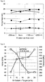
- the layers then have an increasing hardness and a decreasing modulus of elasticity as the silicon content increases, as in FIG Figure 4 shown. There, it is not the concentration ratios in the layers but the concentration ratios Ti / Si in the targets used for the production of the layers that are given.
- the Ti x Si 1-x N layer with at least 15at% Si content of the metallic components is not applied directly to the substrate to be coated but a TiAlN layer as an intermediate layer between the substrate and the layer according to the invention intended.
- This intermediate layer has the advantage, among other things, that it mediates between the less brittle substrate and the extremely hard Ti x Si 1-x N layer, which is loaded with very high internal stresses, with regard to the stress and / or pressure conditions. This means that there is much less flaking and the layer adhesion is improved accordingly.
- Figure 5 shows a series of such two - layer layers according to the invention, the different targets already discussed in accordance with the information in the figure being used for the coating of the Ti x Si 1-x layers.
- a target was used to produce the intermediate layer which comprises 40at% titanium and 60at% aluminum. It has been found that it is particularly advantageous if both layers TiAlN and TiSiN have a (200) texture.
- Such double layers with different Si contents were tested on tools.
- the machining tests were carried out under the following conditions: workpiece steel DIN 1.2344 hardened to 45HRC, tool diameter 10mm solid carbide cutter, cutting speed 220m / min, feed per tooth 0.1mm, axial infeed 10mm, radial infeed 0.5mm. It was measured through how many meters a corresponding tool can work without being damaged.
- Tool which is coated with a commercially available layer survives for a little more than 200m.
- Tools coated with the double layer described above survive for about the same time, with the outer layer only containing 5% silicon. In contrast, the tests showed that the tool survives more than 500m if the outer layer contains at least 15% silicon.
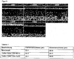
- Table 1 lists the wear values measured for the tools after a cutting path of 140 m. It can be clearly seen that the wear is lowest when coated with 30% silicon.
- a transition layer is provided between the TiAlN intermediate layer and the Ti x Si 1-x layer, which was produced by means of co-sputtering.
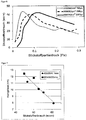
- cosputterning can be carried out reliably in such a way that, for example, the pulse lengths for the different targets are selected in such a way that the maxima of the reactive gas consumption curves are essentially superimposed depending on the pressure prevailing in the coating chamber. This is possible because the pulse duration has a direct influence on the position of the corresponding maxima. This is for an example in Figure 6 shown, where with 3 different pulse durations (0.05ms, 0.2ms and 2ms) it was sputtered in this way it is possible to operate both targets optimally with the same pressure and gas flow conditions prevailing in the chamber.
- the transition layer is implemented as a gradient layer which, with increasing distance from the substrate surface, has a decreasing proportion of TiAlN and an increasing proportion of Ti x Si 1-x N.
- the final Ti x Si 1-x N layer is not a pure Ti x Si 1-x N layer but rather still contains proportions of TiAlN.
- a first Ti x Si 1-x target and a second Ti z Si 1-z target are used for the coating, where 0 x 1 and 0 z 1 , but e.g. ⁇ x, ie first and second target differ in their composition and (x + z) / 2 ⁇ 0.85, so that layers with a Si concentration of ⁇ 15 at% can still be produced.
- both targets can then be operated using the co-sputtering method described above. This allows the Si concentration to be varied during the coating, ie to realize a Si concentration profile.
- the Ti x Si 1-x N layer with at least 15at% Si content of the metallic components is not applied directly to the substrate to be coated, but rather a Cr y Al 1- y N-layer provided as an intermediate layer.
- a chromium content of 40at% and an aluminum content of 60at% have proven to be advantageous.
- This intermediate layer has the advantage, among other things, that it mediates between the less brittle substrate and the extremely hard Ti x Si 1-x N layer, which is loaded with very high internal stresses, with regard to the stress and / or pressure conditions. This means that there is much less flaking and the layer adhesion is improved accordingly.
- x indicates the concentration of Ti expressed in at% and y indicates the concentration of Cr expressed in at% if only the metallic elements are taken into account.
- Such double layers with different Si contents were tested on tools. It was measured by how many meters a corresponding tool can work without being significantly damaged.
- the machining tests were carried out under the following conditions: workpiece steel DIN 1.2379 hardened to 69HRC, tool diameter 2mm solid carbide ball end mill, cutting speed 110m / min, feed per tooth 0.04mm, axial infeed 0.1mm, radial infeed 0.04mm.
- Tool coated with a commercially available layer survives for a little more than 60m.
- tools coated with the double layer described above, with the outer layer containing at least 10% silicon survive for more than 100m. It is interesting that the CrAlN layer should be kept relatively thin. This indicates that the CrAlN layer essentially takes on the function of an adhesive layer.
- a transition layer is provided between the CrAlN intermediate layer and the Ti x Si 1-x layer, which was produced by means of co-sputtering.
- cosputterning can be carried out reliably in such a way that, for example, the pulse lengths for the different targets are selected in such a way that the maxima of the reactive gas consumption curves are essentially superimposed depending on the pressure prevailing in the coating chamber. This is possible because the pulse duration has a direct influence on the position of the corresponding maxima. This is for an example in Figure 6 shown where 3 different pulse durations (0.05ms, 0.2ms and 2ms) were sputtered. In this way it is possible to operate both targets optimally with the same pressure and gas flow conditions prevailing in the chamber.
- the transition layer is implemented as a gradient layer which, with increasing distance from the substrate surface, has a decreasing proportion of CrAlN and an increasing proportion of Ti x Si 1-x N.
- the final Ti x Si 1-x N layer is not a pure Ti x Si 1-x N layer but rather still contains proportions of CrAlN.
- An intermediate layer which comprises TiAlN or CrAlN or TiAlN and CrAlN, is preferably provided between the Ti x Si 1-x N layer and the substrate body of the workpiece.
- the transition layer is produced by means of co-sputtering.
- the Ti x Si 1-x N layer obtained with the coating method according to the invention can be used according to the present invention Invention still contain proportions of TiAlN or CrAlN or TiAlN and CrAlN.
Landscapes
- Chemical & Material Sciences (AREA)
- Engineering & Computer Science (AREA)
- Mechanical Engineering (AREA)
- Chemical Kinetics & Catalysis (AREA)
- Materials Engineering (AREA)
- Metallurgy (AREA)
- Organic Chemistry (AREA)
- Physical Vapour Deposition (AREA)
- Cutting Tools, Boring Holders, And Turrets (AREA)
- Coating By Spraying Or Casting (AREA)
Description
- Die vorliegende Erfindung bezieht sich auf ein Beschichtungsverfahren.
- Silizium ist ein chemisches Element welches im Zusammenhang mit Hartstoffschichten manchmal dazu eingesetzt wird die Schichtspannungen zu erhöhen. Erhöht sich die Schichtspannung so führt dies in der Regel zu einer grösseren Härte der Schicht. Dies kommt beispielsweise auch in Verbindung mit Titannitrid zum Einsatz. Daraus resultieren Schichten welche chemisch durch die Strukturformel TixSi1-xN beschrieben werden können, wobei x die in at% ausgedrückte Konzentration von Ti wenn nur die metallischen Elemente in Betracht gezogen werden ist. Bei dieser Schreibweise addieren sich die in Prozent angegebenen atomaren Konzentrationen zu 100%.
- Solche Schichten lassen sich in sehr harter Form mittels des sogenannten kathodischen Funkenverdampfens herstellen. Dabei wird zwischen einem die metallischen Elemente liefernden Target, welches als Kathode eingesetzt wird und einer Anode ein Funken gezündet über den aus der Targetoberfläche ein Elektronenstrom hoher Dichte herausgezogen wird. Aufgrund der stark lokalisierten sehr hohen Stromdichte an der Targetoberfläche wird lokal die Targetoberfläche stark erhitzt und das Material in ionisierter Form verdampft.
- Das derart verdampfte und ionisierte Material wird dann mit Hilfe einer an die Substrate angelegten negativen Spannung auf die Substrate zu beschleunigt. Wird zusätzlich die Beschichtungskammer ein Reaktivgas eingelassen so verbinden sich die verdampften Ionen mit dem Reaktivgas und bilden eine entsprechende Schicht auf der Substratoberfläche.
- Bei diesem Verfahren kommt es jedoch häufig zu der sogenannten Droplet-Problematik: Aufgrund der plötzlichen lokalen Erhitzung auf der Targetoberfläche kommt es zu einer explosionsartigen Aufschmelzung dieser durch die ganze Tropfen des Targetmaterials in die Umgebung geschleudert werden. Diese Tropfen landen teilweise auf der Substratoberfläche was in der Regel negative Auswirkungen auf die Schichteigenschaften und deren Qualität nach sich zieht. Zwar gibt es inzwischen Methoden, diese Droplets herauszufiltern. Solche Filter lassen die Beschichtungsrate allerdings sehr klein werden und es ist kaum mehr möglich die Beschichtung wirtschaftlich zu betreiben.
- Andererseits führt ein Siliziumanteil von grösser als 15at% sehr häufig während des Funkenverdampfens zur Beschädigung des Targets. Im Extremfall muss dann das Target nach jeder Beschichtung ausgewechselt werden, was wiederum der Wirtschaftlichkeit des Prozesses abträglich ist.
- Diesen Problemen sieht sich der Fachmann beim konventionellen Abscheiden aus der Gasphase mittels Zerstäuben mit Magnetronunterstützung (Magnetron Sputtern) nicht ausgesetzt. Allerdings sind die von der Targetoberfläche durch Ionenbeschuss herausgeschlagenen Partikel nicht oder kaum ionisiert und lassen sich daher auch nicht mit einem an die Substrate angelegten Substratbias zu den Substraten beschleunigen. Entsprechend weissen solche auf konventionelle Art gesputterten Schichten eine relativ geringe Dichte und Härte auf.
- Shtansky et al. zeigt in Surface and Coatings Technology 182 (2004) 204-214 ein Sputterverfahren zur Herstellung von Ti-Si-N Schichten. Eine bekannte Möglichkeit, die Dichte und Härte von Sputterschichten in dem Funkenverdampfen ähnliche Bereiche zu schieben ist das sogenannte HiPIMS Verfahren. HiPIMS = High Power Impulse Magnetron Sputtering). Bei diesem Sputterverfahren wird eine Sputterkathode mit hohen Leistungspulsdichten beaufschlagt, was dazu führt, dass das von der Kathode zerstäubte Material zu einem hohen Prozentsatz ionisiert ist. Wird nun eine negative Spannung an die zu beschichtenden Werkstücke angelegt, so werden diese Ionen in Richtung Werkstücke beschleunigt, was zu sehr dichten Schichten führt.
- Die Sputterkathode muss pulsweise mit Leistung beaufschlagt werden, um ihr Zeit zu geben, den mit der Leistung einhergehenden Wärmeeintrag abzuführen. Beim HiPIMS Verfahren wird als Leistungsquelle daher ein Pulsgenerator benötigt. Dieser Pulsgenerator muss in der Lage sein sehr hohe Leistungspulse abzugeben, die jedoch sehr kurz sind. Die heute erhältlichen Pulsgeneratoren zeigen wenig Flexibilität, was zum Beispiel Pulshöhe und/oder Pulsdauer betrifft. Idealerweise sollte ein Rechteckpuls abgegeben werden. Zumeist ist jedoch die Leistungsabgabe innerhalb eines Pulses stark zeitabhängig, was unmittelbar Einfluss auf die Schichteigenschaften, wie zum Beispiel Härte, Haftung, Eigenspannung etc. hat. Ausserdem wird die Beschichtungsrate durch die Abweichung vom Rechteckprofil negativ beeinflusst.
- Insbesondere werfen diese Schwierigkeiten Fragen hinsichtlich der Reproduzierbarkeit auf.
- Soviel die Erfinder wissen wurde dementsprechend auch noch nicht versucht, TixSi1-xN Schichten mittels des HiPIMS Verfahrens herzustellen.
- Es besteht daher ein Bedürfnis nach einem Verfahren, demgemäss TixSi1-xN Schichten mittels Magnetronzerstäuben bei hoher Leistung hergestellt werden können.
- Erfindungsgemäss werden die Schichten mittels eines Sputterverfahrens hergestellt bei dem es zur konstant hohen Leistungsabgabe der Leistungsquelle kommt. Dabei kommen mehrere Sputterkathoden zum Einsatz. Anders als bei den konventionellen HiPIMS Verfahren wird kein Pulsgenerator eingesetzt sondern es wird zunächst lediglich eine erste Sputterkathode mit der vollen Leistung der Leistungsquelle und damit mit hoher Leistungsdichte beaufschlagt. Anschliessend wird eine zweite Sputterkathode mit den Ausgängen der Leistungsquelle verbunden. Dabei passiert zunächst wenig da die Impedanz der zweiten Sputterkathode zu diesem Zeitpunkt weitaus höher ist als die Impedanz der ersten Sputterkathode. Erst wenn die erste Sputterkathode von den Ausgängen der Leistungsquelle getrennt wird erfolgt die Leistungsabgabe im Wesentlichen über die zweite Sputterkathode. Das entsprechende Hochleistungsmagnetron-Sputterverfahren ist genauer in der
WO 2013060415 beschrieben. Typischerweise wird die Leistungsquelle dabei in der Grössenordnung von 60kW gefahren. Typische Leistungen welchen die Sputterkathoden im zeitlichen Mittel ausgesetzt sind liegen grössenordnungsmässig bei 8kW. - Die Erfinder haben nun völlig überraschend herausgefunden, dass wenn ein solches Verfahren mit TiSi-Targets betrieben wird, welche einen Siliziumanteil von grösser gleich 15at% enthalten es gelingt, reproduzierbar nanokristalline Schichten mit sehr guten mechanischen Eigenschaften zu erzeugen. Besonders interessant ist, dass ab einer Si-Konzentration im Target von 15at% die Nanokristalle im Mittel eine Korngrösse von weniger als 15nm aufweisen, wie in
Figur 1 dargestellt. Dass sich die Konzentrationsverhältnisse im für die Beschichtung verwendeten Target nahezu direkt in der beschichteten Schicht wiederspiegeln ist inFigur 2 dargestellt. Es sei an dieser Stelle angemerkt dass, sobald ein Target mit einer gewissen Si-Konzentration gewählt wurde, sich die Korngrösse über den Stickstoffverbrauch feineinstellen lässt, wieFigur 7 zeigt. - Dass es sich hierbei um ein sehr robustes Phänomen handelt ist an
Figur 3 ersichtlich. Hier wurden die Korngrössen von Schichten vermessen, welche an unterschiedlichen Positionen auf dem rotierenden Karussell beschichtet wurden. Die Messreihe mit den schwarz gefüllten kreisrunden Symbolen bezieht sich auf ein Ti95Si5 -Target. Die Messreihe mit den weiss gefüllten kreisrunden Symbolen bezieht sich auf ein Ti90Si10 -Target. Die Messreihe mit den schwarz gefüllten quadratischen Symbolen bezieht sich auf ein Ti85Si15 -Target. Die Messreihe mit den weiss gefüllten dreieckigen Symbolen bezieht sich auf ein Ti80Si20-Target. Die Messreihe mit den schwarz gefüllten dreieckigen Symbolen bezieht sich auf ein Ti75Si15 -Target. Offensichtlich wird die Korngrösse jeweils über die gesamte Beschichtungshöhe der Kammer eingehalten. - Die Schichten weisen dann mit zunehmendem Siliziumgehalt eine zunehmende Härte und ein abnehmendes E-Modul auf, wie in
Figur 4 dargestellt. Dort sind nicht die Konzentrationsverhältnisse in den Schichten sondern die Konzentrationsverhältnisse Ti/Si in den für die Herstellung der Schichten verwendeten Targets angegeben. - Gemäss einer weiteren Ausführungsform der vorliegenden Erfindung wird die TixSi1-xN - Schicht mit mindestens 15at%-tigem Si Anteil der metallischen Komponenten nicht direkt auf das zu beschichtende Substrat aufgebracht sondern zwischen Substrat und der erfindungsgemässen Schicht eine TiAlN-Schicht als Zwischenschicht vorgesehen. Diese Zwischenschicht hat u.a. den Vorteil, dass sie zwischen dem weniger spröden Substrat und der äusserst harten und mit sehr hohen Eigenspannungen belasteten TixSi1-xN - Schicht hinsichtlich den Spannungs- und/oder Druckverhältnissen vermittelt. Hierdurch kommt es viel weniger zu Abplatzungen und die Schichthaftung ist entsprechend verbessert.
-
Figur 5 zeigt eine Serie solcher erfindungsgemässer Zweischichter, wobei für die Beschichtung der TixSi1-x- Schichten wiederum die bereits besprochenen unterschiedlichen Targets gemäss den Angaben in der Figur verwendet wurden. Deutlich sichtbar in der Serie sind die unterschiedlichen Strukturen der TixSi1-x- Schichten, die steigendem Si-Gehalt immer feiner werden. Im vorliegenden Beispiel wurde zur Herstellung der Zwischenschicht ein Target verwendet, welches 40at% Titan und 60at% Aluminium umfasst. Es wurde festgestellt, dass besonders Vorteilhaft ist wenn beide Schichten TiAlN und TiSiN eine (200) Textur aufweisen. - Es wurden solche Doppelschichten mit unterschiedlichem Si-Gehalt an Werkzeugen getestet. Die Zerspanungstests wurden unter folgenden Bedingungen durchgeführt: Werkstück Stahl DIN 1.2344 gehärtet auf 45HRC, Werkzeug Durchmesser 10mm Vollhartmetallfräser, Schnittgeschwindigkeit 220m/min, Vorschub pro Zahn 0.1mm, axiale Zustellung 10mm, radiale Zustellung 0.5mm. Dabei wurde gemessen durch wieviele Meter sich ein entsprechendes Werkzeug arbeiten kann, ohne Schaden zu nehmen. Werkzeug welches mit einer marktüblichen Schicht beschichtet ist, überlebt für etwas mehr als 200m. In etwa gleich lang überlebt Werkzeug, welches mit der oben beschriebenen Doppelschicht beschichtet ist, wobei die äussere Schicht lediglich 5% Silizium enthält. Demgegenüber zeigten die Tests dass das Werkzeug mehr als 500m überlebt wenn die äussere Schicht zumindest 15% Silizium enthält. In der Tabelle 1 sind die Verschleisswerte gemessen bei den Werkzeugen nach 140m Schneidweg aufgelistet. Man erkennt eindeutig, dass Verschleiss bei der Beschichtung mit 30% Silizium am geringstem ist.
- Gemäss einer weiteren, vorteilhaften Ausführungsform wird zwischen der TiAlN-Zwischenschicht und der TixSi1-x-Schicht eine Übergangsschicht vorgesehen, die mittels Cosputtern hergestellt wurde. Mit dem oben beschriebenen Sputterverfahren lässt sich Cosputtern in zuverlässiger Weise so durchführen, dass beispielsweise die Pulslängen für die unterschiedlichen Targets so gewählt werden, dass die Maxima der Reaktivgasverbrauchkurven in Abhängigkeit vom in der Beschichtungskammer vorherrschenden Druck im Wesentlichen übereinander zu liegen kommen. Dies ist deswegen möglich, weil die Pulsdauer direkt Einfluss auf die Lage der entsprechenden Maxima hat. Dies ist für ein Beispiel in
Figur 6 dargestellt, wo mit 3 unterschiedlichen Pulsdauern (0.05ms, 0.2ms und 2ms) gesputtert wurde auf diese Weise ist es möglich beide Targets bei denselben in der Kammer vorherrschenden Druck und Gasflussverhältnissen optimal zu betreiben. - Gemäss einer weiteren Ausführungsform der vorliegenden Erfindung wird die Übergangsschicht als Gradientenschicht verwirklicht, welche mit zunehmendem Abstand von der Substratoberfläche einen abnehmenden Anteil an TiAlN und einen zunehmenden Anteil an TixSi1-xN besitzt.
- Gemäss einer weiteren Ausführungsform der vorliegenden Erfindung ist die abschliessende TixSi1-xN -Schicht keine reine TixSi1-xN- Schicht sondern enthält noch Anteile an TiAlN.
- Gemäss einer weiteren Ausführungsform der vorliegenden Erfindung wird für die Beschichtung ein erstes TixSi1-x- Target und ein zweites TizSi1-z Target verwendet, wobei 0≤x≤1 und 0≤z≤1 sein kann, aber z≠x ist, d.h. erstes und zweites Target sich in ihrer Zusammensetzung unterscheiden und (x+z)/2 ≤0.85 ist, so dass sich weiterhin Schichten mit einer Si-Konzentration von ≥15at% herstellen lassen. Im Verfahren können dann beide Targets nach der oben beschriebenen Co-sputter-Methodik betrieben werden. Dies gestattet während der Beschichtung die Si-Konzentration zu variieren, d.h. einen Si-Konzentrationsverlauf zu realisieren.
- Ferner haben die Erfinder festgestellt, dass überraschend hervorragende Schichtperformances von erfindungsgemäss abgeschiedenen Schichten sich durch die Verwendung einer CryAl1-yN-Schicht als Zwischenschicht erreichen lassen. Demgemäss werden nachstehend weitere, bevorzugte Ausführungsformen der vorliegenden Erfindung beschrieben, welche CryAl1-yN-Schichten als Zwischenschichten umfassen.
- Gemäss einer weiteren Ausführungsform der vorliegenden Erfindung wird die TixSi1-xN - Schicht mit mindestens 15at%-tigem Si Anteil der metallischen Komponenten nicht direkt auf das zu beschichtende Substrat aufgebracht sondern zwischen Substrat und der erfindungsgemässen Schicht eine CryAl1-yN-Schicht als Zwischenschicht vorgesehen. Dabei hat sich ein Chromanteil von 40at% und ein Aluminiumanteil von 60at% als vorteilhaft herausgestellt. Diese Zwischenschicht hat u.a. den Vorteil, dass sie zwischen dem weniger spröden Substrat und der äusserst harten und mit sehr hohen Eigenspannungen belasteten TixSi1-xN - Schicht hinsichtlich den Spannungs- und/oder Druckverhältnissen vermittelt. Hierdurch kommt es viel weniger zu Abplatzungen und die Schichthaftung ist entsprechend verbessert.
- Im vorigen Abschnitt und in der folgenden Beschreibung gibt x die in at% ausgedrückte Konzentration von Ti und y die in at% ausgedrückte Konzentration an Cr angibt, wenn nur die metallischen Elemente in Betracht gezogen werden.
- Es wurden solche Doppelschichten mit unterschiedlichem Si-Gehalt an Werkzeugen getestet. Dabei wurde gemessen durch wieviele Meter sich ein entsprechendes Werkzeug arbeiten kann, ohne signifikanten Schaden zu nehmen. Die Zerspanungstests wurden unter folgenden Bedingungen durchgeführt: Werkstück Stahl DIN 1.2379 gehärtet auf 69HRC, Werkzeug Durchmesser 2mm Vollhartmetallkugelkopffräser, Schnittgeschwindigkeit 110m/min, Vorschub pro Zahn 0.04mm, axiale Zustellung 0.1mm, radiale Zustellung 0.04mm. Werkzeug welches mit einer marktüblichen Schicht beschichtet ist, überlebt für etwas mehr als 60m. Demgegenüber überlebt Werkzeug, welches mit der oben beschriebenen Doppelschicht beschichtet ist, wobei die äussere Schicht mindestens 10% Silizium enthält, für mehr als 100m. Interessant dabei ist dass die CrAlN-Schicht relativ dünn gehalten werden sollte. Dies deutet darauf hin, dass die CrAlN Schicht im Wesentlichen die Funktion einer Haftschicht übernimmt.
- Gemäss einer weiteren, vorteilhaften Ausführungsform wird zwischen der CrAlN-Zwischenschicht und der TixSi1-x-Schicht eine Übergangsschicht vorgesehen, die mittels Cosputtern hergestellt wurde. Mit dem oben beschriebenen Sputterverfahren lässt sich Cosputtern in zuverlässiger Weise so durchführen, dass beispielsweise die Pulslängen für die unterschiedlichen Targets so gewählt werden, dass die Maxima der Reaktivgasverbrauchkurven in Abhängigkeit vom in der Beschichtungskammer vorherrschenden Druck im Wesentlichen übereinander zu liegen kommen. Dies ist deswegen möglich, weil die Pulsdauer direkt Einfluss auf die Lage der entsprechenden Maxima hat. Dies ist für ein Beispiel in
Figur 6 dargestellt, wo mit 3 unterschiedlichen Pulsdauern (0.05ms, 0.2ms und 2ms) gesputtert wurde. Auf diese Weise ist es möglich beide Targets bei denselben in der Kammer vorherrschenden Druck und Gasflussverhältnissen optimal zu betreiben. - Gemäss einer weiteren Ausführungsform der vorliegenden Erfindung wird die Übergangsschicht als Gradientenschicht verwirklicht, welche mit zunehmendem Abstand von der Substratoberfläche einen abnehmenden Anteil an CrAlN und einen zunehmenden Anteil an TixSi1-xN besitzt.
- Gemäss einer weiteren Ausführungsform der vorliegenden Erfindung ist die abschliessende TixSi1-xN -Schicht keine reine TixSi1-xN- Schicht sondern enthält noch Anteile an CrAlN.
- Die Erfindung betrifft konkret dann ein Verfahren gemäß Anspruch 1 zur Beschichtung eines Werkstücks mit einer Beschichtung, wobei Beschichtung zumindest
eine TixSi1-xN Schicht umfasst, dadurch gekennzeichnet,
dass x<= 0.85 und die TixSi1-xN Schicht Nanokristalle
enthält und die enthaltenen Nanokristalle eine durchschnittliche Korngrösse von nicht mehr als 15nm besitzen
und vorzugsweise eine (200) Textur aufweist. Die
Erfindung betrifft ausserdem ein Verfahren gemäß Anspruch 1 zur Beschichtung
eines Werkstücks mit einer Beschichtung, die zumindest
die vorgenannte TixSi1-xN Schicht umfasst, wobei
das für die Herstellung der TixSi1-xN Schicht eingesetzte Verfahren ein Sputterverfahren ist, bei dem mindestens ein TixSi1-x -Target als Sputtertarget verwendet
wird, wobei x <= 0.85 in Atom-%, und wobei es auf der Targetoberfläche des Sputtertargets zu Stromdichten von mindestens 0.2 A/cm2, vorzugsweise grösser 0.2 A/cm2 kommt. Vorzugsweise ist zwischen der TixSi1-xN Schicht und dem Substratkörper des Werkstücks eine Zwischenschicht vorgesehen, welche TiAlN oder CrAlN oder TiAlN und CrAlN umfasst. - Gemäss einer bevorzugten Ausführungsform eines Verfahrens zur Beschichtung eines Werkstücks gemäss der anspruchs gemäßen Erfindung, bei dem eine Übergangsschicht
abgeschieden werden sollte, wird die Übergangsschicht mittels Co-Sputtern hergestellt. - Wenn es für bestimmte Anwendungen Vorteile bringt, kann die mit dem erfindungsgemäßen Beschichtungsverfahren erhaltene TixSi1-xN Schicht gemäss der vorliegenden
Erfindung noch Anteile an TiAlN oder CrAlN oder TiAlN und CrAlN enthalten. - Je nach Anwendung kann auch möglich sein, dass in den oben genannten Ausführungsformen der vorliegenden Erfindung statt TiAlN oder CrAlN in der Beschichtung andere Metallnitride oder Metallnitrid-basierte Materialien verwendet werden, um gewünschte Schichteigenschaften zu erreichen.
Claims (8)
- Verfahren zur Beschichtung eines Werkstücks mit einer Beschichtung, die zumindest eine TixSi1-xN Schicht umfasst, bei der x ≤ 0.85 ist und wobei die TixSi1-xN Schicht Nanokristalle enthält und die enthaltenen Nanokristalle eine durchschnittliche Korngrösse von nicht mehr als 15nm besitzen, wobei x die in at% ausgedrückte Konzentration von Ti ist, wenn nur die metallischen Elemente in Betracht gezogen werden, dadurch gekennzeichnet dass für die Herstellung der TixSi1-xN Schicht ein Sputterverfahren eingesetzt wird, bei dem mindestens ein TixSi1-x -Target als Sputtertarget verwendet wird, wobei x ≤ 0.85 in Atom% ist, und wobei es auf der Targetoberfläche des Sputtertargets zu Stromdichten von mindestens 0.2 A/cm2, vorzugsweise grösser 0.2 A/cm2 kommt, dass zunächst eine erste Sputterkathode mit der vollen Leistung der Leistungsquelle und damit mit hoher Leistungsdichte beaufschlagt wird, dass anschliessend eine zweite Sputterkathode mit den Ausgängen der Leistungsquelle verbunden wird, wobei die Leistungsabgabe erst dann, wenn die erste Sputterkathode von den Ausgängen der Leistungsquelle getrennt wird, im Wesentlichen über die zweite Sputterkathode erfolgt und dass die Leistungsquelle konstant hohe Leistung abgibt.
- Verfahren nach Anspruch 1, dadurch gekennzeichnet, dass das Verfahren zur Beschichtung eines Werkstücks eingesetzt wird bei dem zwischen der TixSi1-xN Schicht und dem Substratkörper des Werkstücks eine Zwischenschicht mit TiAIN vorgesehen ist.
- Verfahren nach Anspruch 1, dadurch gekennzeichnet, dass das Verfahren zur Beschichtung eines Werkstücks eingesetzt wird, bei dem zwischen der Zwischenschicht und der TixSi1-xN Schicht eine Übergangsschicht vorgesehen ist, welche sowohl TiAIN als auch TixSi1-xN enthält.
- Verfahren nach Anspruch 1, dadurch gekennzeichnet, dass das Verfahren zur Beschichtung eines Werkstücks eingesetzt wird, bei dem die Übergangsschicht eine Gradientenschicht ist, deren Siliziumanteil mit zunehmendem Abstand von der Substratoberfläche zunimmt.
- Verfahren nach Anspruch 1, dadurch gekennzeichnet, dass das Verfahren zur Beschichtung eines Werkstücks eingesetzt wird, bei dem zwischen der TixSi1-xN Schicht und dem Substratkörper des Werkstücks eine Zwischenschicht mit CryAl1-yN vorgesehen ist, wobei y die in at% ausgedrückte Konzentration an Cr angibt, wenn nur die metallischen Elemente in Betracht gezogen werden.
- Verfahren nach Anspruch 5, dadurch gekennzeichnet, dass das Verfahren zur Beschichtung eines Werkstücks eingesetzt wird, bei dem zwischen der Zwischenschicht und der TixSi1-xN Schicht eine Übergangsschicht vorgesehen ist, welche sowohl CryAl1-yN als auch TixSi1-xN enthält.
- Verfahren nach Anspruch 6, dadurch gekennzeichnet, dass das Verfahren zur Beschichtung eines Werkstücks eingesetzt wird, bei dem die Übergangsschicht eine Gradientenschicht ist, deren Siliziumanteil mit zunehmendem Abstand von der Substratoberfläche zunimmt.
- Verfahren zur Beschichtung eines Werkstücks nach einem der vorangehenden Ansprüche 3, 4, 6 oder 7, dadurch gekennzeichnet, dass die Übergangsschicht mittels Co-Sputtern hergestellt wird.
Priority Applications (1)
| Application Number | Priority Date | Filing Date | Title |
|---|---|---|---|
| PL14737148T PL3017079T5 (pl) | 2013-07-03 | 2014-07-01 | Sposób wytwarzania warstw tixsi1-xn |
Applications Claiming Priority (3)
| Application Number | Priority Date | Filing Date | Title |
|---|---|---|---|
| DE201310011071 DE102013011071A1 (de) | 2013-07-03 | 2013-07-03 | TixSi1-xN Schichten mit CryAl1-yN Haftschicht und ihre Herstellung |
| DE102013011073.4A DE102013011073A1 (de) | 2013-07-03 | 2013-07-03 | TlxSi1-xN Schichten und ihre Herstellung |
| PCT/EP2014/001792 WO2015000581A1 (de) | 2013-07-03 | 2014-07-01 | Tixsi1-xn schichten und ihre herstellung |
Publications (3)
| Publication Number | Publication Date |
|---|---|
| EP3017079A1 EP3017079A1 (de) | 2016-05-11 |
| EP3017079B1 EP3017079B1 (de) | 2017-04-12 |
| EP3017079B2 true EP3017079B2 (de) | 2020-09-09 |
Family
ID=51167846
Family Applications (1)
| Application Number | Title | Priority Date | Filing Date |
|---|---|---|---|
| EP14737148.8A Active EP3017079B2 (de) | 2013-07-03 | 2014-07-01 | Verfahren zur herstellung von tixsi1-xn schichten |
Country Status (17)
| Country | Link |
|---|---|
| US (1) | US9840768B2 (de) |
| EP (1) | EP3017079B2 (de) |
| JP (1) | JP6122975B2 (de) |
| KR (2) | KR101891900B1 (de) |
| CN (1) | CN105392911B (de) |
| BR (1) | BR112015032169B1 (de) |
| CA (1) | CA2916784C (de) |
| ES (1) | ES2630316T5 (de) |
| IL (1) | IL243136A (de) |
| MX (1) | MX361325B (de) |
| MY (1) | MY187100A (de) |
| PH (1) | PH12015502753B1 (de) |
| PL (1) | PL3017079T5 (de) |
| PT (1) | PT3017079T (de) |
| RU (1) | RU2674179C2 (de) |
| SG (1) | SG11201510417RA (de) |
| WO (1) | WO2015000581A1 (de) |
Families Citing this family (3)
| Publication number | Priority date | Publication date | Assignee | Title |
|---|---|---|---|---|
| CN108883481B (zh) * | 2016-03-30 | 2020-01-14 | 三菱日立工具株式会社 | 包覆切削工具 |
| WO2019065397A1 (ja) * | 2017-09-27 | 2019-04-04 | 三菱日立ツール株式会社 | 被覆切削工具 |
| CN115125486B (zh) * | 2022-07-27 | 2024-01-02 | 安徽工业大学 | 一种含有多层结构的高强韧纳米复合涂层及其制备方法 |
Citations (10)
| Publication number | Priority date | Publication date | Assignee | Title |
|---|---|---|---|---|
| EP1174528A2 (de) † | 2000-07-13 | 2002-01-23 | Hitachi Tool Engineering Ltd. | Mehrlagig beschichtetes Schneidwerkzeug |
| US20060147728A1 (en) † | 2004-05-03 | 2006-07-06 | Yaogen Shen | Multi-layered superhard nanocomposite coatings |
| WO2007129021A1 (en) † | 2006-05-02 | 2007-11-15 | Sheffield Hallam University | High power impulse magnetron sputtering vapour deposition |
| EP2072637A2 (de) † | 2007-12-21 | 2009-06-24 | Sandvik Intellectual Property AB | Schneidwerkzeug und Verfahren zum Herstellen |
| EP2336382A1 (de) † | 2009-12-04 | 2011-06-22 | Sandvik Intellectual Property AB | Beschichtetes Schneidewerkzeug |
| WO2011149580A1 (en) † | 2010-05-28 | 2011-12-01 | Kennametal Inc. | Multilayer nitride hard coatings |
| WO2012143087A1 (de) † | 2011-04-20 | 2012-10-26 | Oerlikon Trading Ag, Trübbach | Hochleistungszerstäubungsquelle |
| WO2012143110A1 (en) † | 2011-04-20 | 2012-10-26 | Oerlikon Trading Ag, Trübbach | High power impulse magnetron sputtering method providing enhanced ionization of the sputtered particles and apparatus for its implementation |
| WO2013060415A1 (de) † | 2011-10-28 | 2013-05-02 | Oerlikon Trading AG,Trübbach | Verfahren zur bereitstellung sequenzieller leistungspulse |
| DE102012209293B3 (de) † | 2012-06-01 | 2013-06-20 | Helmholtz-Zentrum Dresden - Rossendorf E.V. | Sputterverfahren |
Family Cites Families (32)
| Publication number | Priority date | Publication date | Assignee | Title |
|---|---|---|---|---|
| JPH07197246A (ja) * | 1993-12-28 | 1995-08-01 | Mitsubishi Materials Corp | 成膜中にパーティクル発生の少ないスパッタリング用Tiシリサイド焼結ターゲット材 |
| JPH0867971A (ja) * | 1994-08-30 | 1996-03-12 | Mitsubishi Materials Corp | モザイク状Tiシリサイドターゲット材 |
| DE19625577A1 (de) | 1996-06-27 | 1998-01-02 | Vaw Motor Gmbh | Aluminium-Gußteil und Verfahren zu seiner Herstellung |
| JP3996809B2 (ja) | 2002-07-11 | 2007-10-24 | 住友電工ハードメタル株式会社 | 被覆切削工具 |
| US6906295B2 (en) * | 2003-02-20 | 2005-06-14 | National Material L.P. | Foodware with multilayer stick resistant ceramic coating and method of making |
| AU2003903853A0 (en) | 2003-07-25 | 2003-08-07 | Antoine Bittar | Barriers, materials and processes for solar selective surfaces |
| JP2005344148A (ja) * | 2004-06-01 | 2005-12-15 | Sumitomo Electric Ind Ltd | 耐摩耗性被膜およびこれを用いた表面被覆切削工具 |
| US7790003B2 (en) * | 2004-10-12 | 2010-09-07 | Southwest Research Institute | Method for magnetron sputter deposition |
| US7348074B2 (en) * | 2005-04-01 | 2008-03-25 | Oc Oerlikon Balzers Ag | Multilayer hard coating for tools |
| SE0500994L (sv) * | 2005-04-29 | 2006-10-30 | Seco Tools Ab | Tunt slitstarkt skikt |
| CN101326303B (zh) | 2005-10-18 | 2012-07-18 | 西南研究院 | 抗侵蚀涂层 |
| US7939172B2 (en) * | 2006-05-17 | 2011-05-10 | G & H Technologies, Llc | Wear resistant vapor deposited coating, method of coating deposition and applications therefor |
| RU2327811C1 (ru) * | 2006-11-14 | 2008-06-27 | Государственное образовательное учреждение высшего профессионального образования "Ульяновский государственный технический университет" | Способ получения многослойного покрытия для режущего инструмента |
| SE0602814L (sv) * | 2006-12-27 | 2008-06-28 | Sandvik Intellectual Property | Skärverktyg med multiskiktbeläggning |
| WO2008146727A1 (ja) | 2007-05-30 | 2008-12-04 | Sumitomo Electric Hardmetal Corp. | 表面被覆切削工具 |
| CN101855035B (zh) | 2007-10-12 | 2013-03-27 | 日立工具股份有限公司 | 被覆有硬质被膜的部件及其制造方法 |
| ES2658849T3 (es) * | 2008-07-09 | 2018-03-12 | Oerlikon Surface Solutions Ltd., Pfäffikon | Sistema de recubrimiento, pieza de trabajo recubierta y método de fabricación de la misma |
| ATE535629T1 (de) * | 2008-07-29 | 2011-12-15 | Sulzer Metaplas Gmbh | Gepulstes hochleistungs-magnetronsputterverfahren sowie hochleistungs-elektroenergiequelle |
| JP5156971B2 (ja) | 2009-03-17 | 2013-03-06 | Smc株式会社 | 溶損防止用被覆部材 |
| SE533883C2 (sv) | 2009-06-01 | 2011-02-22 | Seco Tools Ab | Nanolaminerat belagt skärverktyg |
| WO2010150335A1 (ja) * | 2009-06-22 | 2010-12-29 | 株式会社タンガロイ | 被覆立方晶窒化硼素焼結体工具 |
| JP5190971B2 (ja) * | 2009-12-16 | 2013-04-24 | 住友電気工業株式会社 | 被膜、切削工具および被膜の製造方法 |
| PT2524066T (pt) | 2010-01-11 | 2018-12-24 | Iscar Ltd | Ferramenta de corte revestida |
| JP2011167793A (ja) * | 2010-02-18 | 2011-09-01 | Mitsubishi Materials Corp | 表面被覆切削工具 |
| RU2428509C1 (ru) * | 2010-04-13 | 2011-09-10 | Государственное образовательное учреждение высшего профессионального образования "Ульяновский государственный технический университет" | Способ получения многослойного покрытия для режущего инструмента |
| RU2419680C1 (ru) * | 2010-04-20 | 2011-05-27 | Государственное образовательное учреждение высшего профессионального образования "Ульяновский государственный технический университет" | Способ получения многослойного покрытия для режущего инструмента |
| WO2011131756A1 (en) * | 2010-04-23 | 2011-10-27 | Seco Tools Ab | Pvd coating for metal machining |
| US8673435B2 (en) * | 2010-07-06 | 2014-03-18 | Tungaloy Corporation | Coated cBN sintered body tool |
| DE102010034321B4 (de) | 2010-08-09 | 2017-04-06 | Technische Universität Dresden | Verfahren zur Herstellung einer Hartstoffbeschichtung auf metallischen, keramischen oder hartmetallischen Bauteilen sowie eine mit dem Verfahren hergestellte Hartstoffbeschichtung |
| CN103228383B (zh) | 2010-11-26 | 2016-08-03 | 住友电工硬质合金株式会社 | 表面被覆烧结体 |
| DE102011053372A1 (de) | 2011-09-07 | 2013-03-07 | Walter Ag | Werkzeug mit chromhaltiger Funktionsschicht |
| CN104272429B (zh) * | 2011-12-05 | 2016-08-24 | 欧瑞康表面解决方案股份公司,普费菲孔 | 用于反应溅射的方法 |
-
2014
- 2014-07-01 RU RU2016102845A patent/RU2674179C2/ru active
- 2014-07-01 SG SG11201510417RA patent/SG11201510417RA/en unknown
- 2014-07-01 KR KR1020167002703A patent/KR101891900B1/ko active Active
- 2014-07-01 WO PCT/EP2014/001792 patent/WO2015000581A1/de not_active Ceased
- 2014-07-01 KR KR1020177026135A patent/KR102178189B1/ko active Active
- 2014-07-01 MY MYPI2015704719A patent/MY187100A/en unknown
- 2014-07-01 JP JP2015563197A patent/JP6122975B2/ja active Active
- 2014-07-01 ES ES14737148T patent/ES2630316T5/es active Active
- 2014-07-01 CN CN201480037761.2A patent/CN105392911B/zh active Active
- 2014-07-01 US US14/902,826 patent/US9840768B2/en active Active
- 2014-07-01 EP EP14737148.8A patent/EP3017079B2/de active Active
- 2014-07-01 CA CA2916784A patent/CA2916784C/en not_active Expired - Fee Related
- 2014-07-01 MX MX2015017033A patent/MX361325B/es active IP Right Grant
- 2014-07-01 PT PT147371488T patent/PT3017079T/pt unknown
- 2014-07-01 PL PL14737148T patent/PL3017079T5/pl unknown
- 2014-07-01 BR BR112015032169-0A patent/BR112015032169B1/pt active IP Right Grant
-
2015
- 2015-12-09 PH PH12015502753A patent/PH12015502753B1/en unknown
- 2015-12-15 IL IL243136A patent/IL243136A/en active IP Right Grant
Patent Citations (11)
| Publication number | Priority date | Publication date | Assignee | Title |
|---|---|---|---|---|
| EP1174528A2 (de) † | 2000-07-13 | 2002-01-23 | Hitachi Tool Engineering Ltd. | Mehrlagig beschichtetes Schneidwerkzeug |
| US20060147728A1 (en) † | 2004-05-03 | 2006-07-06 | Yaogen Shen | Multi-layered superhard nanocomposite coatings |
| WO2007129021A1 (en) † | 2006-05-02 | 2007-11-15 | Sheffield Hallam University | High power impulse magnetron sputtering vapour deposition |
| EP2072637A2 (de) † | 2007-12-21 | 2009-06-24 | Sandvik Intellectual Property AB | Schneidwerkzeug und Verfahren zum Herstellen |
| EP2336382A1 (de) † | 2009-12-04 | 2011-06-22 | Sandvik Intellectual Property AB | Beschichtetes Schneidewerkzeug |
| WO2011149580A1 (en) † | 2010-05-28 | 2011-12-01 | Kennametal Inc. | Multilayer nitride hard coatings |
| WO2012143087A1 (de) † | 2011-04-20 | 2012-10-26 | Oerlikon Trading Ag, Trübbach | Hochleistungszerstäubungsquelle |
| WO2012143110A1 (en) † | 2011-04-20 | 2012-10-26 | Oerlikon Trading Ag, Trübbach | High power impulse magnetron sputtering method providing enhanced ionization of the sputtered particles and apparatus for its implementation |
| WO2013060415A1 (de) † | 2011-10-28 | 2013-05-02 | Oerlikon Trading AG,Trübbach | Verfahren zur bereitstellung sequenzieller leistungspulse |
| DE102011117177A1 (de) † | 2011-10-28 | 2013-05-02 | Oerlikon Trading Ag, Trübbach | Verfahren zur Bereitstellung sequenzieller Leistungspulse |
| DE102012209293B3 (de) † | 2012-06-01 | 2013-06-20 | Helmholtz-Zentrum Dresden - Rossendorf E.V. | Sputterverfahren |
Non-Patent Citations (7)
| Title |
|---|
| BOBZIN K. ET AL: "Advantages of nanocomposite coatings deposited by high power pulse magnetron sputtering technology", JOURNAL OF MATERIALS PROCESSING TECHNOLOGY , vol. 209, no. 1, 1 January 2009 (2009-01-01), pages 165 - 170, DOI: 10.1016/j.jmatprotec.2008.01.035 † |
| BOBZIN K. ET AL: "Properties of (Ti,Al,Si)N Coatings for High Demanding Metal Cutting Applications Deposited by HPPMS in an Industrial Coating Unit", PLASMA PROCESS. POLYM. , vol. 6, 1 January 2009 (2009-01-01), pages S124 - S128, DOI: 10.1002/ppap.200930408 † |
| EHIASARIAN A.P. ET AL: "Influence of high power impulse magnetron sputtering plasma ionization on the microstructure of TiN thin films", JOURNAL OF APPLIED PHYSICS, vol. 109, 1 January 2011 (2011-01-01), pages 104314-1 - 104314-15, DOI: 10.1063/1.3579443 † |
| EHIASARIAN A.P.: "High-power impulse magnetron sputtering and its applications", PURE APPL. CHEM., vol. 82, no. 6, 1 January 2010 (2010-01-01), pages 1247 - 1258, DOI: 10.1351/PAC-CON-09-10-43 † |
| SHTANSKY D.V. ET AL: "Comparative investigation of Ti–Si–N films magnetron sputtered using Ti5Si3+Ti and Ti5Si3+TiN targets", SURFACE AND COATINGS TECHNOLOGY, vol. 182, no. 2-3, 22 April 2004 (2004-04-22), pages 204 - 214, DOI: 10.1016/j.surfcoat.2003.08.052 † |
| VAZ F ET AL: "Structural analysis of Ti1-xSixNy nanocomposite films prepared by reactive magnetron sputtering", SURFACE AND COATINGS TECHNOLOGY, ELSEVIER, AMSTERDAM, NL, vol. 120-121, 1 November 1999 (1999-11-01), pages 166 - 172, ISSN: 0257-8972, [retrieved on 19991101] † |
| Wikipedia Article on High-power impulse Magnetron sputtering (revision of page edited 20-02-2013) † |
Also Published As
Similar Documents
| Publication | Publication Date | Title |
|---|---|---|
| EP3215651B1 (de) | Pvd verfahren zur herstellung eines schneidwerkzeugs mit mehrlagiger beschichtung | |
| DE102005063536B4 (de) | Hartstoff - Schichtsystem | |
| DE19517120C2 (de) | Beschichtetes Teil mit ausgezeichneter Härte und Haftung, seine Verwendung und Verfahren zur Herstellung | |
| EP3056587B1 (de) | VHM-Schaftfräser mit TiAlN-ZrN-Beschichtung | |
| EP2893053B1 (de) | Verfahren zur herstellung einer metallborocarbidschicht auf einem substrat | |
| WO2009127344A1 (de) | Beschichtungsverfahren, werkstück oder werkzeug und dessen verwendung | |
| DE3825399C2 (de) | PVD- oder Plasma- CVD-Beschichtung und Verfahren zu ihrer Herstellung | |
| EP3017078B1 (de) | Tib2-schichten und ihre herstellung | |
| EP2653583A1 (de) | Beschichtungsverfahren zur Abscheidung eines Schichtsystems auf einem Substrat, sowie Substrat mit einem Schichtsystem | |
| DE102011117994A1 (de) | HIPIMS-Schichten | |
| EP3445890B1 (de) | Ticn mit reduzierten wachstumsdefekten mittels hipims | |
| EP2912206A1 (de) | Bauteil mit einer beschichtung und verfahren zu seiner herstellung | |
| WO2014063677A1 (de) | Bauteil mit einer beschichtung und verfahren zu seiner herstellung | |
| EP3017079B2 (de) | Verfahren zur herstellung von tixsi1-xn schichten | |
| DE102010034321B4 (de) | Verfahren zur Herstellung einer Hartstoffbeschichtung auf metallischen, keramischen oder hartmetallischen Bauteilen sowie eine mit dem Verfahren hergestellte Hartstoffbeschichtung | |
| EP2872666A1 (de) | Hochleistungsimpulsbeschichtungsverfahren | |
| EP2286643B1 (de) | Vorrichtung und verfahren zum hochleistungs-puls-gasfluss-sputtern | |
| EP3019640B1 (de) | Target zur reaktiven sputter-abscheidung elektrisch-isolierender schichten | |
| DE102013011073A1 (de) | TlxSi1-xN Schichten und ihre Herstellung | |
| EP2989654B1 (de) | Lichtbogenverdampfungs-beschichtungsquelle mit permanentmagnet | |
| DE102019206414A1 (de) | Verfahren und Vorrichtung zur Herstellung von Arbeits- und/oder Dressierwalzen und beschichtete Arbeits- und/oder Dressierwalze | |
| DE102013011071A1 (de) | TixSi1-xN Schichten mit CryAl1-yN Haftschicht und ihre Herstellung | |
| EP3768871A1 (de) | Magnetronsputtervorrichtung | |
| DE102011108088B4 (de) | Werkzeug mit einer nitridischen Hartstoffschicht sowie Verfahren zu dessen Herstellung | |
| DE102022125083A1 (de) | Verfahren zur Beschichtung eines Werkzeugteils eines spanabhebenden Werkzeugs |
Legal Events
| Date | Code | Title | Description |
|---|---|---|---|
| PUAI | Public reference made under article 153(3) epc to a published international application that has entered the european phase |
Free format text: ORIGINAL CODE: 0009012 |
|
| 17P | Request for examination filed |
Effective date: 20160129 |
|
| AK | Designated contracting states |
Kind code of ref document: A1 Designated state(s): AL AT BE BG CH CY CZ DE DK EE ES FI FR GB GR HR HU IE IS IT LI LT LU LV MC MK MT NL NO PL PT RO RS SE SI SK SM TR |
|
| AX | Request for extension of the european patent |
Extension state: BA ME |
|
| RIN1 | Information on inventor provided before grant (corrected) |
Inventor name: KURAPOV, DENIS Inventor name: KRASSNITZER, SIEGFRIED |
|
| GRAP | Despatch of communication of intention to grant a patent |
Free format text: ORIGINAL CODE: EPIDOSNIGR1 |
|
| INTG | Intention to grant announced |
Effective date: 20160623 |
|
| GRAJ | Information related to disapproval of communication of intention to grant by the applicant or resumption of examination proceedings by the epo deleted |
Free format text: ORIGINAL CODE: EPIDOSDIGR1 |
|
| DAX | Request for extension of the european patent (deleted) | ||
| RAP1 | Party data changed (applicant data changed or rights of an application transferred) |
Owner name: OERLIKON SURFACE SOLUTIONS AG, PFAEFFIKON |
|
| GRAP | Despatch of communication of intention to grant a patent |
Free format text: ORIGINAL CODE: EPIDOSNIGR1 |
|
| INTG | Intention to grant announced |
Effective date: 20161019 |
|
| GRAS | Grant fee paid |
Free format text: ORIGINAL CODE: EPIDOSNIGR3 |
|
| STAA | Information on the status of an ep patent application or granted ep patent |
Free format text: STATUS: GRANT OF PATENT IS INTENDED |
|
| GRAA | (expected) grant |
Free format text: ORIGINAL CODE: 0009210 |
|
| STAA | Information on the status of an ep patent application or granted ep patent |
Free format text: STATUS: THE PATENT HAS BEEN GRANTED |
|
| AK | Designated contracting states |
Kind code of ref document: B1 Designated state(s): AL AT BE BG CH CY CZ DE DK EE ES FI FR GB GR HR HU IE IS IT LI LT LU LV MC MK MT NL NO PL PT RO RS SE SI SK SM TR |
|
| REG | Reference to a national code |
Ref country code: GB Ref legal event code: FG4D Free format text: NOT ENGLISH |
|
| REG | Reference to a national code |
Ref country code: CH Ref legal event code: EP |
|
| REG | Reference to a national code |
Ref country code: IE Ref legal event code: FG4D Free format text: LANGUAGE OF EP DOCUMENT: GERMAN |
|
| REG | Reference to a national code |
Ref country code: AT Ref legal event code: REF Ref document number: 883965 Country of ref document: AT Kind code of ref document: T Effective date: 20170515 |
|
| REG | Reference to a national code |
Ref country code: DE Ref legal event code: R096 Ref document number: 502014003430 Country of ref document: DE |
|
| REG | Reference to a national code |
Ref country code: RO Ref legal event code: EPE |
|
| REG | Reference to a national code |
Ref country code: NL Ref legal event code: FP Ref country code: PT Ref legal event code: SC4A Ref document number: 3017079 Country of ref document: PT Date of ref document: 20170719 Kind code of ref document: T Free format text: AVAILABILITY OF NATIONAL TRANSLATION Effective date: 20170712 |
|
| REG | Reference to a national code |
Ref country code: SE Ref legal event code: TRGR |
|
| REG | Reference to a national code |
Ref country code: FR Ref legal event code: PLFP Year of fee payment: 4 |
|
| REG | Reference to a national code |
Ref country code: ES Ref legal event code: FG2A Ref document number: 2630316 Country of ref document: ES Kind code of ref document: T3 Effective date: 20170821 |
|
| REG | Reference to a national code |
Ref country code: LT Ref legal event code: MG4D |
|
| PG25 | Lapsed in a contracting state [announced via postgrant information from national office to epo] |
Ref country code: LT Free format text: LAPSE BECAUSE OF FAILURE TO SUBMIT A TRANSLATION OF THE DESCRIPTION OR TO PAY THE FEE WITHIN THE PRESCRIBED TIME-LIMIT Effective date: 20170412 Ref country code: HR Free format text: LAPSE BECAUSE OF FAILURE TO SUBMIT A TRANSLATION OF THE DESCRIPTION OR TO PAY THE FEE WITHIN THE PRESCRIBED TIME-LIMIT Effective date: 20170412 Ref country code: NO Free format text: LAPSE BECAUSE OF FAILURE TO SUBMIT A TRANSLATION OF THE DESCRIPTION OR TO PAY THE FEE WITHIN THE PRESCRIBED TIME-LIMIT Effective date: 20170712 Ref country code: GR Free format text: LAPSE BECAUSE OF FAILURE TO SUBMIT A TRANSLATION OF THE DESCRIPTION OR TO PAY THE FEE WITHIN THE PRESCRIBED TIME-LIMIT Effective date: 20170713 |
|
| PG25 | Lapsed in a contracting state [announced via postgrant information from national office to epo] |
Ref country code: BG Free format text: LAPSE BECAUSE OF FAILURE TO SUBMIT A TRANSLATION OF THE DESCRIPTION OR TO PAY THE FEE WITHIN THE PRESCRIBED TIME-LIMIT Effective date: 20170712 Ref country code: IS Free format text: LAPSE BECAUSE OF FAILURE TO SUBMIT A TRANSLATION OF THE DESCRIPTION OR TO PAY THE FEE WITHIN THE PRESCRIBED TIME-LIMIT Effective date: 20170812 Ref country code: LV Free format text: LAPSE BECAUSE OF FAILURE TO SUBMIT A TRANSLATION OF THE DESCRIPTION OR TO PAY THE FEE WITHIN THE PRESCRIBED TIME-LIMIT Effective date: 20170412 Ref country code: RS Free format text: LAPSE BECAUSE OF FAILURE TO SUBMIT A TRANSLATION OF THE DESCRIPTION OR TO PAY THE FEE WITHIN THE PRESCRIBED TIME-LIMIT Effective date: 20170412 |
|
| REG | Reference to a national code |
Ref country code: SK Ref legal event code: T3 Ref document number: E 24736 Country of ref document: SK |
|
| REG | Reference to a national code |
Ref country code: DE Ref legal event code: R026 Ref document number: 502014003430 Country of ref document: DE |
|
| PLBI | Opposition filed |
Free format text: ORIGINAL CODE: 0009260 |
|
| REG | Reference to a national code |
Ref country code: HU Ref legal event code: AG4A Ref document number: E033853 Country of ref document: HU |
|
| PG25 | Lapsed in a contracting state [announced via postgrant information from national office to epo] |
Ref country code: EE Free format text: LAPSE BECAUSE OF FAILURE TO SUBMIT A TRANSLATION OF THE DESCRIPTION OR TO PAY THE FEE WITHIN THE PRESCRIBED TIME-LIMIT Effective date: 20170412 Ref country code: DK Free format text: LAPSE BECAUSE OF FAILURE TO SUBMIT A TRANSLATION OF THE DESCRIPTION OR TO PAY THE FEE WITHIN THE PRESCRIBED TIME-LIMIT Effective date: 20170412 |
|
| PLAX | Notice of opposition and request to file observation + time limit sent |
Free format text: ORIGINAL CODE: EPIDOSNOBS2 |
|
| 26 | Opposition filed |
Opponent name: IHI IONBOND AG Effective date: 20180112 |
|
| PG25 | Lapsed in a contracting state [announced via postgrant information from national office to epo] |
Ref country code: SM Free format text: LAPSE BECAUSE OF FAILURE TO SUBMIT A TRANSLATION OF THE DESCRIPTION OR TO PAY THE FEE WITHIN THE PRESCRIBED TIME-LIMIT Effective date: 20170412 |
|
| REG | Reference to a national code |
Ref country code: IE Ref legal event code: MM4A |
|
| PG25 | Lapsed in a contracting state [announced via postgrant information from national office to epo] |
Ref country code: IE Free format text: LAPSE BECAUSE OF NON-PAYMENT OF DUE FEES Effective date: 20170701 |
|
| PG25 | Lapsed in a contracting state [announced via postgrant information from national office to epo] |
Ref country code: SI Free format text: LAPSE BECAUSE OF FAILURE TO SUBMIT A TRANSLATION OF THE DESCRIPTION OR TO PAY THE FEE WITHIN THE PRESCRIBED TIME-LIMIT Effective date: 20170412 |
|
| PLAF | Information modified related to communication of a notice of opposition and request to file observations + time limit |
Free format text: ORIGINAL CODE: EPIDOSCOBS2 |
|
| PLBB | Reply of patent proprietor to notice(s) of opposition received |
Free format text: ORIGINAL CODE: EPIDOSNOBS3 |
|
| REG | Reference to a national code |
Ref country code: FR Ref legal event code: PLFP Year of fee payment: 5 |
|
| PG25 | Lapsed in a contracting state [announced via postgrant information from national office to epo] |
Ref country code: MT Free format text: LAPSE BECAUSE OF FAILURE TO SUBMIT A TRANSLATION OF THE DESCRIPTION OR TO PAY THE FEE WITHIN THE PRESCRIBED TIME-LIMIT Effective date: 20170412 |
|
| PG25 | Lapsed in a contracting state [announced via postgrant information from national office to epo] |
Ref country code: MC Free format text: LAPSE BECAUSE OF FAILURE TO SUBMIT A TRANSLATION OF THE DESCRIPTION OR TO PAY THE FEE WITHIN THE PRESCRIBED TIME-LIMIT Effective date: 20170412 |
|
| PG25 | Lapsed in a contracting state [announced via postgrant information from national office to epo] |
Ref country code: CY Free format text: LAPSE BECAUSE OF FAILURE TO SUBMIT A TRANSLATION OF THE DESCRIPTION OR TO PAY THE FEE WITHIN THE PRESCRIBED TIME-LIMIT Effective date: 20170412 |
|
| PG25 | Lapsed in a contracting state [announced via postgrant information from national office to epo] |
Ref country code: MK Free format text: LAPSE BECAUSE OF FAILURE TO SUBMIT A TRANSLATION OF THE DESCRIPTION OR TO PAY THE FEE WITHIN THE PRESCRIBED TIME-LIMIT Effective date: 20170412 |
|
| APBM | Appeal reference recorded |
Free format text: ORIGINAL CODE: EPIDOSNREFNO |
|
| APBP | Date of receipt of notice of appeal recorded |
Free format text: ORIGINAL CODE: EPIDOSNNOA2O |
|
| APAH | Appeal reference modified |
Free format text: ORIGINAL CODE: EPIDOSCREFNO |
|
| APBU | Appeal procedure closed |
Free format text: ORIGINAL CODE: EPIDOSNNOA9O |
|
| PG25 | Lapsed in a contracting state [announced via postgrant information from national office to epo] |
Ref country code: AL Free format text: LAPSE BECAUSE OF FAILURE TO SUBMIT A TRANSLATION OF THE DESCRIPTION OR TO PAY THE FEE WITHIN THE PRESCRIBED TIME-LIMIT Effective date: 20170412 |
|
| PGFP | Annual fee paid to national office [announced via postgrant information from national office to epo] |
Ref country code: PT Payment date: 20200629 Year of fee payment: 7 Ref country code: TR Payment date: 20200630 Year of fee payment: 7 |
|
| PUAH | Patent maintained in amended form |
Free format text: ORIGINAL CODE: 0009272 |
|
| STAA | Information on the status of an ep patent application or granted ep patent |
Free format text: STATUS: PATENT MAINTAINED AS AMENDED |
|
| REG | Reference to a national code |
Ref country code: CH Ref legal event code: AELC |
|
| PGFP | Annual fee paid to national office [announced via postgrant information from national office to epo] |
Ref country code: SK Payment date: 20200630 Year of fee payment: 7 |
|
| 27A | Patent maintained in amended form |
Effective date: 20200909 |
|
| AK | Designated contracting states |
Kind code of ref document: B2 Designated state(s): AL AT BE BG CH CY CZ DE DK EE ES FI FR GB GR HR HU IE IS IT LI LT LU LV MC MK MT NL NO PL PT RO RS SE SI SK SM TR |
|
| REG | Reference to a national code |
Ref country code: DE Ref legal event code: R102 Ref document number: 502014003430 Country of ref document: DE |
|
| PGFP | Annual fee paid to national office [announced via postgrant information from national office to epo] |
Ref country code: RO Payment date: 20200701 Year of fee payment: 7 Ref country code: ES Payment date: 20200807 Year of fee payment: 7 Ref country code: FI Payment date: 20200721 Year of fee payment: 7 |
|
| REG | Reference to a national code |
Ref country code: CH Ref legal event code: NV Representative=s name: VALIPAT S.A. C/O BOVARD SA NEUCHATEL, CH |
|
| REG | Reference to a national code |
Ref country code: NL Ref legal event code: FP |
|
| PG25 | Lapsed in a contracting state [announced via postgrant information from national office to epo] |
Ref country code: SK Free format text: LAPSE BECAUSE OF FAILURE TO SUBMIT A TRANSLATION OF THE DESCRIPTION OR TO PAY THE FEE WITHIN THE PRESCRIBED TIME-LIMIT Effective date: 20200909 |
|
| PG25 | Lapsed in a contracting state [announced via postgrant information from national office to epo] |
Ref country code: PT Free format text: LAPSE BECAUSE OF FAILURE TO SUBMIT A TRANSLATION OF THE DESCRIPTION OR TO PAY THE FEE WITHIN THE PRESCRIBED TIME-LIMIT Effective date: 20210121 |
|
| REG | Reference to a national code |
Ref country code: ES Ref legal event code: DC2A Ref document number: 2630316 Country of ref document: ES Kind code of ref document: T5 Effective date: 20210618 |
|
| REG | Reference to a national code |
Ref country code: FI Ref legal event code: MAE |
|
| PG25 | Lapsed in a contracting state [announced via postgrant information from national office to epo] |
Ref country code: FI Free format text: LAPSE BECAUSE OF NON-PAYMENT OF DUE FEES Effective date: 20210701 |
|
| PG25 | Lapsed in a contracting state [announced via postgrant information from national office to epo] |
Ref country code: RO Free format text: LAPSE BECAUSE OF NON-PAYMENT OF DUE FEES Effective date: 20210701 |
|
| REG | Reference to a national code |
Ref country code: ES Ref legal event code: FD2A Effective date: 20220905 |
|
| PG25 | Lapsed in a contracting state [announced via postgrant information from national office to epo] |
Ref country code: ES Free format text: LAPSE BECAUSE OF NON-PAYMENT OF DUE FEES Effective date: 20210702 |
|
| PGFP | Annual fee paid to national office [announced via postgrant information from national office to epo] |
Ref country code: PL Payment date: 20250618 Year of fee payment: 12 |
|
| PGFP | Annual fee paid to national office [announced via postgrant information from national office to epo] |
Ref country code: CZ Payment date: 20250623 Year of fee payment: 12 |
|
| PGFP | Annual fee paid to national office [announced via postgrant information from national office to epo] |
Ref country code: HU Payment date: 20250626 Year of fee payment: 12 |
|
| PGFP | Annual fee paid to national office [announced via postgrant information from national office to epo] |
Ref country code: NL Payment date: 20250724 Year of fee payment: 12 Ref country code: LU Payment date: 20250724 Year of fee payment: 12 |
|
| PGFP | Annual fee paid to national office [announced via postgrant information from national office to epo] |
Ref country code: DE Payment date: 20250728 Year of fee payment: 12 |
|
| PGFP | Annual fee paid to national office [announced via postgrant information from national office to epo] |
Ref country code: IT Payment date: 20250721 Year of fee payment: 12 |
|
| PGFP | Annual fee paid to national office [announced via postgrant information from national office to epo] |
Ref country code: BE Payment date: 20250724 Year of fee payment: 12 Ref country code: GB Payment date: 20250722 Year of fee payment: 12 |
|
| PGFP | Annual fee paid to national office [announced via postgrant information from national office to epo] |
Ref country code: AT Payment date: 20250718 Year of fee payment: 12 Ref country code: FR Payment date: 20250725 Year of fee payment: 12 |
|
| PGFP | Annual fee paid to national office [announced via postgrant information from national office to epo] |
Ref country code: CH Payment date: 20250801 Year of fee payment: 12 Ref country code: SE Payment date: 20250725 Year of fee payment: 12 |