EP3010045A1 - Semiconductor device and a method of manufacturing same - Google Patents
Semiconductor device and a method of manufacturing same Download PDFInfo
- Publication number
- EP3010045A1 EP3010045A1 EP15189734.5A EP15189734A EP3010045A1 EP 3010045 A1 EP3010045 A1 EP 3010045A1 EP 15189734 A EP15189734 A EP 15189734A EP 3010045 A1 EP3010045 A1 EP 3010045A1
- Authority
- EP
- European Patent Office
- Prior art keywords
- silicon oxide
- oxide film
- type
- region
- semiconductor device
- Prior art date
- Legal status (The legal status is an assumption and is not a legal conclusion. Google has not performed a legal analysis and makes no representation as to the accuracy of the status listed.)
- Withdrawn
Links
Images
Classifications
-
- H—ELECTRICITY
- H01—ELECTRIC ELEMENTS
- H01L—SEMICONDUCTOR DEVICES NOT COVERED BY CLASS H10
- H01L21/00—Processes or apparatus adapted for the manufacture or treatment of semiconductor or solid state devices or of parts thereof
- H01L21/02—Manufacture or treatment of semiconductor devices or of parts thereof
- H01L21/02104—Forming layers
- H01L21/02365—Forming inorganic semiconducting materials on a substrate
- H01L21/02518—Deposited layers
- H01L21/02521—Materials
- H01L21/02524—Group 14 semiconducting materials
- H01L21/02529—Silicon carbide
-
- H—ELECTRICITY
- H01—ELECTRIC ELEMENTS
- H01L—SEMICONDUCTOR DEVICES NOT COVERED BY CLASS H10
- H01L21/00—Processes or apparatus adapted for the manufacture or treatment of semiconductor or solid state devices or of parts thereof
- H01L21/02—Manufacture or treatment of semiconductor devices or of parts thereof
- H01L21/02104—Forming layers
- H01L21/02107—Forming insulating materials on a substrate
- H01L21/02109—Forming insulating materials on a substrate characterised by the type of layer, e.g. type of material, porous/non-porous, pre-cursors, mixtures or laminates
- H01L21/02112—Forming insulating materials on a substrate characterised by the type of layer, e.g. type of material, porous/non-porous, pre-cursors, mixtures or laminates characterised by the material of the layer
- H01L21/02123—Forming insulating materials on a substrate characterised by the type of layer, e.g. type of material, porous/non-porous, pre-cursors, mixtures or laminates characterised by the material of the layer the material containing silicon
- H01L21/02164—Forming insulating materials on a substrate characterised by the type of layer, e.g. type of material, porous/non-porous, pre-cursors, mixtures or laminates characterised by the material of the layer the material containing silicon the material being a silicon oxide, e.g. SiO2
-
- H—ELECTRICITY
- H01—ELECTRIC ELEMENTS
- H01L—SEMICONDUCTOR DEVICES NOT COVERED BY CLASS H10
- H01L21/00—Processes or apparatus adapted for the manufacture or treatment of semiconductor or solid state devices or of parts thereof
- H01L21/02—Manufacture or treatment of semiconductor devices or of parts thereof
- H01L21/02104—Forming layers
- H01L21/02107—Forming insulating materials on a substrate
- H01L21/02225—Forming insulating materials on a substrate characterised by the process for the formation of the insulating layer
- H01L21/02227—Forming insulating materials on a substrate characterised by the process for the formation of the insulating layer formation by a process other than a deposition process
- H01L21/0223—Forming insulating materials on a substrate characterised by the process for the formation of the insulating layer formation by a process other than a deposition process formation by oxidation, e.g. oxidation of the substrate
- H01L21/02233—Forming insulating materials on a substrate characterised by the process for the formation of the insulating layer formation by a process other than a deposition process formation by oxidation, e.g. oxidation of the substrate of the semiconductor substrate or a semiconductor layer
- H01L21/02236—Forming insulating materials on a substrate characterised by the process for the formation of the insulating layer formation by a process other than a deposition process formation by oxidation, e.g. oxidation of the substrate of the semiconductor substrate or a semiconductor layer group IV semiconductor
-
- H—ELECTRICITY
- H01—ELECTRIC ELEMENTS
- H01L—SEMICONDUCTOR DEVICES NOT COVERED BY CLASS H10
- H01L21/00—Processes or apparatus adapted for the manufacture or treatment of semiconductor or solid state devices or of parts thereof
- H01L21/02—Manufacture or treatment of semiconductor devices or of parts thereof
- H01L21/02104—Forming layers
- H01L21/02107—Forming insulating materials on a substrate
- H01L21/02225—Forming insulating materials on a substrate characterised by the process for the formation of the insulating layer
- H01L21/02227—Forming insulating materials on a substrate characterised by the process for the formation of the insulating layer formation by a process other than a deposition process
- H01L21/02255—Forming insulating materials on a substrate characterised by the process for the formation of the insulating layer formation by a process other than a deposition process formation by thermal treatment
-
- H—ELECTRICITY
- H01—ELECTRIC ELEMENTS
- H01L—SEMICONDUCTOR DEVICES NOT COVERED BY CLASS H10
- H01L21/00—Processes or apparatus adapted for the manufacture or treatment of semiconductor or solid state devices or of parts thereof
- H01L21/02—Manufacture or treatment of semiconductor devices or of parts thereof
- H01L21/02104—Forming layers
- H01L21/02107—Forming insulating materials on a substrate
- H01L21/02225—Forming insulating materials on a substrate characterised by the process for the formation of the insulating layer
- H01L21/0226—Forming insulating materials on a substrate characterised by the process for the formation of the insulating layer formation by a deposition process
- H01L21/02263—Forming insulating materials on a substrate characterised by the process for the formation of the insulating layer formation by a deposition process deposition from the gas or vapour phase
- H01L21/02271—Forming insulating materials on a substrate characterised by the process for the formation of the insulating layer formation by a deposition process deposition from the gas or vapour phase deposition by decomposition or reaction of gaseous or vapour phase compounds, i.e. chemical vapour deposition
-
- H—ELECTRICITY
- H01—ELECTRIC ELEMENTS
- H01L—SEMICONDUCTOR DEVICES NOT COVERED BY CLASS H10
- H01L23/00—Details of semiconductor or other solid state devices
- H01L23/28—Encapsulations, e.g. encapsulating layers, coatings, e.g. for protection
- H01L23/29—Encapsulations, e.g. encapsulating layers, coatings, e.g. for protection characterised by the material, e.g. carbon
- H01L23/291—Oxides or nitrides or carbides, e.g. ceramics, glass
-
- H—ELECTRICITY
- H01—ELECTRIC ELEMENTS
- H01L—SEMICONDUCTOR DEVICES NOT COVERED BY CLASS H10
- H01L23/00—Details of semiconductor or other solid state devices
- H01L23/28—Encapsulations, e.g. encapsulating layers, coatings, e.g. for protection
- H01L23/31—Encapsulations, e.g. encapsulating layers, coatings, e.g. for protection characterised by the arrangement or shape
- H01L23/3157—Partial encapsulation or coating
- H01L23/3192—Multilayer coating
-
- H—ELECTRICITY
- H10—SEMICONDUCTOR DEVICES; ELECTRIC SOLID-STATE DEVICES NOT OTHERWISE PROVIDED FOR
- H10D—INORGANIC ELECTRIC SEMICONDUCTOR DEVICES
- H10D62/00—Semiconductor bodies, or regions thereof, of devices having potential barriers
- H10D62/10—Shapes, relative sizes or dispositions of the regions of the semiconductor bodies; Shapes of the semiconductor bodies
- H10D62/102—Constructional design considerations for preventing surface leakage or controlling electric field concentration
- H10D62/103—Constructional design considerations for preventing surface leakage or controlling electric field concentration for increasing or controlling the breakdown voltage of reverse-biased devices
- H10D62/105—Constructional design considerations for preventing surface leakage or controlling electric field concentration for increasing or controlling the breakdown voltage of reverse-biased devices by having particular doping profiles, shapes or arrangements of PN junctions; by having supplementary regions, e.g. junction termination extension [JTE]
- H10D62/106—Constructional design considerations for preventing surface leakage or controlling electric field concentration for increasing or controlling the breakdown voltage of reverse-biased devices by having particular doping profiles, shapes or arrangements of PN junctions; by having supplementary regions, e.g. junction termination extension [JTE] having supplementary regions doped oppositely to or in rectifying contact with regions of the semiconductor bodies, e.g. guard rings with PN or Schottky junctions
-
- H—ELECTRICITY
- H10—SEMICONDUCTOR DEVICES; ELECTRIC SOLID-STATE DEVICES NOT OTHERWISE PROVIDED FOR
- H10D—INORGANIC ELECTRIC SEMICONDUCTOR DEVICES
- H10D62/00—Semiconductor bodies, or regions thereof, of devices having potential barriers
- H10D62/10—Shapes, relative sizes or dispositions of the regions of the semiconductor bodies; Shapes of the semiconductor bodies
- H10D62/102—Constructional design considerations for preventing surface leakage or controlling electric field concentration
- H10D62/112—Constructional design considerations for preventing surface leakage or controlling electric field concentration for preventing surface leakage due to surface inversion layers, e.g. by using channel stoppers
-
- H—ELECTRICITY
- H10—SEMICONDUCTOR DEVICES; ELECTRIC SOLID-STATE DEVICES NOT OTHERWISE PROVIDED FOR
- H10D—INORGANIC ELECTRIC SEMICONDUCTOR DEVICES
- H10D62/00—Semiconductor bodies, or regions thereof, of devices having potential barriers
- H10D62/80—Semiconductor bodies, or regions thereof, of devices having potential barriers characterised by the materials
- H10D62/83—Semiconductor bodies, or regions thereof, of devices having potential barriers characterised by the materials being Group IV materials, e.g. B-doped Si or undoped Ge
- H10D62/832—Semiconductor bodies, or regions thereof, of devices having potential barriers characterised by the materials being Group IV materials, e.g. B-doped Si or undoped Ge being Group IV materials comprising two or more elements, e.g. SiGe
- H10D62/8325—Silicon carbide
-
- H—ELECTRICITY
- H10—SEMICONDUCTOR DEVICES; ELECTRIC SOLID-STATE DEVICES NOT OTHERWISE PROVIDED FOR
- H10D—INORGANIC ELECTRIC SEMICONDUCTOR DEVICES
- H10D8/00—Diodes
- H10D8/01—Manufacture or treatment
- H10D8/043—Manufacture or treatment of planar diodes
-
- H—ELECTRICITY
- H10—SEMICONDUCTOR DEVICES; ELECTRIC SOLID-STATE DEVICES NOT OTHERWISE PROVIDED FOR
- H10D—INORGANIC ELECTRIC SEMICONDUCTOR DEVICES
- H10D8/00—Diodes
- H10D8/01—Manufacture or treatment
- H10D8/051—Manufacture or treatment of Schottky diodes
-
- H—ELECTRICITY
- H10—SEMICONDUCTOR DEVICES; ELECTRIC SOLID-STATE DEVICES NOT OTHERWISE PROVIDED FOR
- H10D—INORGANIC ELECTRIC SEMICONDUCTOR DEVICES
- H10D8/00—Diodes
- H10D8/411—PN diodes having planar bodies
Definitions
- the invention relates to a semiconductor device using silicon carbide as the semiconductor material thereof, and a method of manufacturing the same.
- SiC silicon carbide
- Si silicon carbide
- a termination structure such as Junction Termination Extension (JTE), or Field Limiting Ring (FLR), etc.
- JTE Junction Termination Extension
- FLR Field Limiting Ring
- blocking state is meant a state where a high potential difference occurs across the main electrodes of the power device, and no current flows between the primary electrodes.
- respective signs “p + “, “p”, and “p - " indicate that the conductivity type of a semiconductor is P-type, and respective impurity carrier concentrations become relatively lower in that order.
- respective signs “n + “, “n”, and “n - " indicate that the conductivity type of a semiconductor is N-type, and respective impurity carrier concentrations become relatively lower in that order.
- Fig. 4 is a longitudinal sectional view showing an example of a conventional Si diode having a JTE.
- a p + type guard ring region 3, a p-type JTE region 4, and an n + type field stop region 5 are formed on the upper surface of an n - type drift layer 2 formed over an n + type substrate 1.
- An underside electrode 7 is formed on the underside of the n + type substrate 1.
- a surface electrode 8, a passivation film 6, and a floating electrode 9 are formed above the n - type drift layer 2 in such a way as to be in contact with the upper surface of the n - type drift layer 2.
- the floating electrode 9 is electrically coupled to the n + type field stop region 5.
- the SiC semiconductor device has the problem of an increase in leakage current, and breakage of a passivation film because of high electric fields applied on the passivation film.
- carriers accelerated by the high electric-fields are injected into the passivation film, thereby causing traps to be generated in the passivation film, whereupon a leakage current flows via the traps through tunneling, etc.
- large current flows, thereby leading to the breakage of the passivation film. Accordingly, with the termination of a power device using an SiC semiconductor substrate, there is the need for taking it into account that a high electric-field is applied to not only a semiconductor junction structure, such as JTE and FLR, but also to the passivation film.
- Patent Literature 1 Japanese Patent Application Laid-Open No. Hei 11 (1999) -330496
- Patent Literature 2 Japanese Patent Application Laid-Open No. 2013 - 42054
- the passivation film on a p-type impurity region, forming the termination structure is of a multi-layer film structure made up of a silicon oxide film in contact with the semiconductor SiC, and a high dielectric film over the silicon oxide film.
- the passivation film over a p-type impurity region, forming the termination structure is of a multi-layer film structure made up of a first silicon oxide film in contact with SiC, a metal insulating film not less than 0. 3 nm, not more than 10 nm, in thickness, provided on the first silicon oxide film, and a second silicon oxide film provided on the metal insulating film.
- the termination structure of the SiC power device since the high dielectric film, and the metal-oxide film, in addition to the silicon oxide film, are used for preparation of the passivation film, various materials for use in preparing those films are required, or a manufacturing process becomes complex, thereby causing an increase in production cost.
- an object of the present invention to provide an SiC semiconductor device capable of obtaining high blocking voltage, and high reliability, while suppressing an increase in production cost.
- a semiconductor device composed of a semiconductor SiC, having a termination region disposed around an active region, the upper surface of the termination region being covered with a passivation film.
- the passivation film includes a first silicon oxide film in contact with the upper surface of the termination region, a second silicon oxide film deposited on the first silicon oxide film, so as to be in contact with the first silicon oxide film, and a third silicon oxide film deposited on the second silicon oxide film, so as to be in contact with the second silicon oxide film.
- a method of manufacturing a semiconductor device composed of a semiconductor SiC, incorporating a termination region disposed around an active region, an upper surface of the termination region being covered with a passivation film includes a first step of forming a sacrificial oxide film on a semiconductor surface with thermal oxidation, a second step of forming a first silicon oxide film functioning as the passivation film, on the termination region, by making use of the sacrificial oxide film formed in the first step, a third step of forming a second silicon oxide film over the first thermal silicon oxide film formed by CVD in the second step, and a fourth step of forming a third silicon oxide film functioning as the passivation film over the second silicon oxide film formed by CVD in the third step.
- the passivation film includes the first through the third silicon oxide films, an electric field applied on the passivation film is relaxed, and the passivation film can be provided without the need for a particular process and material, so that production cost can be reduced.
- the method of manufacturing the semiconductor device includes the step of forming the first silicon oxide film functioning as the passivation film by making use of the sacrificial oxidized film, so that the production cost of an SiC semiconductor device can be reduced.
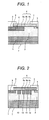
- Fig. 1 is a longitudinal sectional view showing a termination region of an SiC semiconductor device according to one embodiment of the present invention.
- a termination structure according to the present embodiment is applicable to a power device such as a high blocking voltage diode, and a high blocking voltage MOSFET, etc.
- an n - type drift layer 2 in contact with an n + type substrate 1 is provided on the n + type substrate 1.
- the n + type substrate 1 together with the n - type drift layer 2 constitutes an n + n - junction.
- the n - type drift layer 2 is formed by use of the epitaxial growth method, and so forth.
- a p-type JTE region 4 in contact with the n - type drift layer 2, and a p + type guard ring region 3 shallower in depth than the p-type JTE region 4, being in contact with the p-type JTE region 4, are provided on the upper surface of the n - type drift layer 2.
- an n + type field stop region 5 is provided on the upper surface of the n - type drift layer 2.
- the n - type drift layer 2 lies between the p-type JTE region 4, and the n + type field stop region 5, on the upper surface of the n - type drift layer 2.
- the p-type JTE region 4 is separated from the n + type field stop region 5 without coming into contact with each other. A passivation film, and so forth will be described later on.
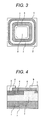
- Fig. 3 shows a plan view of the semiconductor device according to the present embodiment.
- the p + type guard ring region 3, the p-type JTE region 4, and the n + type field stop region 5 each are a single circle in planar shape.
- the central part of the semiconductor device is an active region of the power device such as a diode, a MOSFET, and so forth. However, detailed configuration thereof is omitted in Fig.
- the p + type guard ring region 3, the p-type JTE region 4, and the n + type field stop region 5 are disposed in that order starting from the central part of the n - type drift layer 2 toward the end thereof in such a way as to surround the active region positioned at the central part of the n - type drift layer 2, in the semiconductor device.
- a region positioned around the active region, in a semiconductor chip of the semiconductor device, that is, the region incorporating the p + type guard ring region 3, the p-type JTE region 4, and the n + type field stop region 5 is the termination region.
- the active region controls the main current, and the termination region relaxes an electric field.
- the n + type field stop region 5 is a semiconductor region for preventing the electric field applied on the semiconductor device from reaching the end of the semiconductor chip of the semiconductor device, the n + type field stop region 5 being a semiconductor region formed by introducing an n-type impurity ⁇ for example, phosphorous (P) ⁇ into the upper surface of the n - type drift layer 2 with ion implantation.
- an underside electrode 7 is provided on the underside of the n + type substrate 1, the underside electrode 7 serving as the main electrode in electrical contact with the n + type substrate 1, and a surface electrode 8 is provided on the upper surface of the n - type drift layer 2, the surface electrode 8 serving as the main electrode in electrical contact with the p + type guard ring region 3.
- a floating electrode 9 in electrical contact with the upper surface of the n - type drift layer 2 is provided above the upper surface of the n - type drift layer 2. The floating electrode 9 is separated from the underside electrode 7, and the surface electrode 8, respectively, the floating electrode 9 being in a floating-potential state without being connected to either an external electrode or an external circuit, in the present embodiment.
- the underside electrode 7, the surface electrode 8, and the floating electrode 9 each are made of a conductive material such as aluminum (Al), etc. Further, the floating electrode 9 is capable of equalizing the potential of the n + type field stop region 5, thereby enhancing reliability in a field-stop action of the n + type field stop region 5.
- a passivation film 6 is positioned between the surface electrode 8 and the floating electrode 9, on the upper surface of the n - type drift layer 2.
- the surface electrode 8 and the floating electrode 9 are provided such that respective parts thereof overlie the surface of the passivation film 6.
- the passivation film 6 is provided so as to extend across the surface of an end part of the p + type guard ring region 3, the surface of the p-type JTE region 4, the surface of a part of the n - type drift layer 2, interposed between the p-type JTE region 4 and the n + type field stop region 5, and the surface of an end part of the n + type field stop region 5 in such a way as to cover these surfaces.
- the passivation film 6 is provided across a range from directly above the part of the p + type guard ring region 3 up to directly above the part of the n + type field stop region 5, thereby covering the whole surface of the p-type JTE region 4, and the whole surface of the part of the n - type drift layer 2, interposed between the p-type JTE region 4 and the n + type field stop region 5, within the termination region.
- the passivation film 6 is composed of a thermal silicon oxide film 6a, a silicon oxide film 6b formed by deposition including LPCVD (Low Pressure Chemical Vapor Deposition) or PECVD (Plasma Enhanced Chemical Vapor Deposition) to be subsequently put into a vitrification process, and a silicon oxide film 6c formed by deposition including LPCVD or PECVD, which are stacked upward in that order from the upper surface of the n - type drift layer 2.
- LPCVD Low Pressure Chemical Vapor Deposition
- PECVD Pullasma Enhanced Chemical Vapor Deposition
- the thermal silicon oxide film 6a in a first layer of the passivation film 6 is in contact with the surface of the end part of the p + type guard ring region 3, the surface of the p-type JTE region 4, the surface of the part of the n - type drift layer 2, interposed between the p-type JTE region 4 and the n + type field stop region 5, and the surface of the end part of the n + type field stop region 5, and the CVD silicon oxide film 6b in a second layer of the passivation film 6 is deposited so as to be in contact with the upper surface of the thermal silicon oxide film 6a, while covering the whole surface of the thermal silicon oxide film 6a, whereas the CVD silicon oxide film 6c in a third layer of the passivation film 6 is deposited so as to be in contact with the upper surface of the CVD silicon oxide film 6b, while covering the whole upper surface of the CVD silicon oxide film 6b.
- the passivation film 6 according to the embodiment shown in Fig. 1 includes only three layers of inorganic films composed of silicon oxide, however, the upper surface of the passivation film 6 may be covered with a protective film made of resin such as polyimide, and polyamide, etc.
- the thermal silicon oxide film 6a of the passivation film 6 is made of a thermal oxide film formed in a sacrificial oxidation process applied for removal of damage incurred due to the ion implantation in the surface of the semiconductor SiC, that is, use is made of a portion of a sacrificial oxide film without removal. Accordingly, the thermal silicon oxide film 6a can be provided without addition of a thermally oxidation process in order to form the passivation film. For this reason, it is possible to obtain the termination structure in which stable blocking voltage can be obtained, and leakage-current is low, without causing an increase in production cost. Further, with the present embodiment, the ion implantation is adopted in order to form the p + type guard ring region 3, the p-type JTE region 4, and the n + type field stop region 5.
- the passivation film 6 is made up of three layers, that is, plural layers of the silicon oxide films laid up in decreasing order of compactness in film quality, traps hardly generate in the passivation film. For this reason, it is possible to suppress an increase in leakage current and breakage of the passivation film.
- the passivation film according to the present embodiment is made up of the three layers of the silicon oxide films as described above, the electric field applied on the passivation film is relaxed, and the passivation film can be provided without the need for a particular process and material, so that production cost can be reduced.
- the thermal silicon oxide film is provided over the surface of the semiconductor SiC, and two layers of the CVD oxide films, that is, plural layers thereof are additionally deposited on the thermal silicon oxide film, so that the surface of the semiconductor, that is, the surface of the n - type drift layer 2 which is lightly doped, in particular, can be rendered more stable, and the passivation film can be easily increased in thickness.
- the SiC semiconductor device can have higher blocking voltage, while stabilizing the blocking voltage, thereby enhancing reliability.
- the passivation film 6 is formed by the following steps of a manufacturing process:
- the passivation film can be provided without addition of a thermal oxidation step for formation of the thermal oxide film for use in passivation, and without the need for a particular process and material, so that production cost can be reduced.
- the present embodiment differs from the first embodiment in that a termination region has the FLR structure.
- a portion of the upper surface of an n - type drift layer 2, interposed between a p + type guard ring region 3 and an n + type field stop region 5, is provided with four pieces of p-type FLR regions 10.
- a portion of the n - type drift layer 2 is interposed between the p + type guard ring region 3 and the p-type FLR region 10 in close proximity thereto, between two pieces of the p-type FLR regions 10 in close proximity to each other, and between the n + type field stop region 5 and the p-type FLR region 10 in close proximity thereto, respectively.
- the p + type guard ring region 3, the four pieces of the p-type FLR regions 10, and the n + type field stop region 5 are separated each other. Further, the number of the pieces of the p-type FLR regions 10 can be optionally set in accordance with blocking voltage as desired.
- the planar pattern of the present embodiment shows that the four pieces of the p-type FLR regions 10, each being annular in shape, are provided in place of the p-type JTE region 4, shown in Fig. 3 , in such a way as to surround the active region between the p + type guard ring region 3 and the n + type field stop region 5, in the termination region.
- a passivation film 6 is composed of a thermal silicon oxide film 6a, and CVD silicon oxide films 6b and 6c, stacked upward in two layers in that order, over the thermal silicon oxide film 6a, as is the case with the first embodiment.
- the passivation film 6 is positioned between the surface electrode 8 and a floating electrode 9, over the upper surface of the n - type drift layer 2.
- the surface electrode 8 and the floating electrode 9 are provided such that respective parts thereof overlie the surface of the passivation film 6.
- the passivation film 6 is provided so as to extend across the surface of an end part of the p + type guard ring region 3, the surface of each of the four pieces of the p-type FLR regions 10, the surface of a portion of the n - type drift layer 2, interposed between the p + type guard ring region 3 and the p-type FLR region 10 in close proximity thereto, the surface of a portion of the n - type drift layer 2, interposed between two pieces of the p-type FLR regions 10 in close proximity to each other, the surface of a portion of the n - type drift layer 2, interposed between an end part of the n + type field stop region 5 and the p-type FLR region 10 in close proximity thereto, and the surface of the end part of the n + type field stop region 5, in such a way as to cover these surfaces.
- the second embodiment shown in Fig. 2 is similar to the first embodiment shown in Fig. 1 in respect of configuration and a manufacturing method.
- the second embodiment it is possible to obtain the termination structure in which stable blocking voltage can be obtained, and leakage current is kept low, without causing an increase in production cost, as is the case with the first embodiment.
- a pn junction diode, a Schottky barrier diode, a composite-type diode provided with both a pn-junction and Schottky barrier, a switching device, such as MOSFET, IGBT, etc., are applicable to the semiconductor device provided in the active region.
- the conductivity types p, n of a semiconductor region may be reversed to n, p, respectively.
Landscapes
- Engineering & Computer Science (AREA)
- Computer Hardware Design (AREA)
- Physics & Mathematics (AREA)
- Condensed Matter Physics & Semiconductors (AREA)
- General Physics & Mathematics (AREA)
- Microelectronics & Electronic Packaging (AREA)
- Power Engineering (AREA)
- Manufacturing & Machinery (AREA)
- Chemical & Material Sciences (AREA)
- Ceramic Engineering (AREA)
- Chemical Kinetics & Catalysis (AREA)
- Electrodes Of Semiconductors (AREA)
- Formation Of Insulating Films (AREA)
Applications Claiming Priority (1)
| Application Number | Priority Date | Filing Date | Title |
|---|---|---|---|
| JP2014209618A JP2016081981A (ja) | 2014-10-14 | 2014-10-14 | 半導体装置及びその製造方法 |
Publications (1)
| Publication Number | Publication Date |
|---|---|
| EP3010045A1 true EP3010045A1 (en) | 2016-04-20 |
Family
ID=54329411
Family Applications (1)
| Application Number | Title | Priority Date | Filing Date |
|---|---|---|---|
| EP15189734.5A Withdrawn EP3010045A1 (en) | 2014-10-14 | 2015-10-14 | Semiconductor device and a method of manufacturing same |
Country Status (3)
| Country | Link |
|---|---|
| US (1) | US20160104614A1 (enExample) |
| EP (1) | EP3010045A1 (enExample) |
| JP (1) | JP2016081981A (enExample) |
Families Citing this family (3)
| Publication number | Priority date | Publication date | Assignee | Title |
|---|---|---|---|---|
| JP6547844B2 (ja) * | 2015-12-18 | 2019-07-24 | 富士電機株式会社 | 炭化珪素半導体基板、炭化珪素半導体基板の製造方法、半導体装置および半導体装置の製造方法 |
| US9998109B1 (en) | 2017-05-15 | 2018-06-12 | Cree, Inc. | Power module with improved reliability |
| CN115602703B (zh) | 2021-07-09 | 2025-09-23 | 丰田自动车株式会社 | 半导体装置以及半导体装置的制造方法 |
Citations (7)
| Publication number | Priority date | Publication date | Assignee | Title |
|---|---|---|---|---|
| JPH11330496A (ja) | 1998-05-07 | 1999-11-30 | Hitachi Ltd | 半導体装置 |
| US20070001176A1 (en) * | 2005-06-29 | 2007-01-04 | Ward Allan Iii | Environmentally robust passivation structures for high-voltage silicon carbide semiconductor devices |
| EP1873839A2 (en) * | 2006-06-30 | 2008-01-02 | Kabushiki Kaisha Toshiba | Semiconductor device |
| US20100163888A1 (en) * | 2008-12-30 | 2010-07-01 | Stmicroelectronics S.R.L | Manufacturing process of a power electronic device integrated in a semiconductor substrate with wide band gap and electronic device thus obtained |
| US20110193101A1 (en) * | 2010-02-10 | 2011-08-11 | Kabushiki Kaisha Toshiba | Semiconductor device and method for manufacturing semiconductor device |
| JP2013042054A (ja) | 2011-08-19 | 2013-02-28 | Hitachi Ltd | 半導体装置 |
| US20130149850A1 (en) * | 2011-12-07 | 2013-06-13 | Sumitomo Electric Industries, Ltd. | Method for manufacturing semiconductor device |
Family Cites Families (9)
| Publication number | Priority date | Publication date | Assignee | Title |
|---|---|---|---|---|
| JPH07249770A (ja) * | 1994-03-10 | 1995-09-26 | Toshiba Corp | 半導体装置及びその製造方法 |
| JPH11103070A (ja) * | 1997-08-01 | 1999-04-13 | Sony Corp | 薄膜トランジスタ |
| US7625603B2 (en) * | 2003-11-14 | 2009-12-01 | Robert Bosch Gmbh | Crack and residue free conformal deposited silicon oxide with predictable and uniform etching characteristics |
| KR101190942B1 (ko) * | 2008-02-12 | 2012-10-12 | 미쓰비시덴키 가부시키가이샤 | 탄화규소 반도체 장치 |
| JP2010161241A (ja) * | 2009-01-08 | 2010-07-22 | Toyota Motor Corp | 半導体装置および半導体装置の製造方法 |
| JP5223773B2 (ja) * | 2009-05-14 | 2013-06-26 | 三菱電機株式会社 | 炭化珪素半導体装置の製造方法 |
| JP2011040431A (ja) * | 2009-08-06 | 2011-02-24 | Panasonic Corp | 半導体装置およびその製造方法 |
| JP5443908B2 (ja) * | 2009-09-09 | 2014-03-19 | 株式会社東芝 | 半導体装置の製造方法 |
| US9991399B2 (en) * | 2012-10-04 | 2018-06-05 | Cree, Inc. | Passivation structure for semiconductor devices |
-
2014
- 2014-10-14 JP JP2014209618A patent/JP2016081981A/ja active Pending
-
2015
- 2015-10-08 US US14/878,711 patent/US20160104614A1/en not_active Abandoned
- 2015-10-14 EP EP15189734.5A patent/EP3010045A1/en not_active Withdrawn
Patent Citations (7)
| Publication number | Priority date | Publication date | Assignee | Title |
|---|---|---|---|---|
| JPH11330496A (ja) | 1998-05-07 | 1999-11-30 | Hitachi Ltd | 半導体装置 |
| US20070001176A1 (en) * | 2005-06-29 | 2007-01-04 | Ward Allan Iii | Environmentally robust passivation structures for high-voltage silicon carbide semiconductor devices |
| EP1873839A2 (en) * | 2006-06-30 | 2008-01-02 | Kabushiki Kaisha Toshiba | Semiconductor device |
| US20100163888A1 (en) * | 2008-12-30 | 2010-07-01 | Stmicroelectronics S.R.L | Manufacturing process of a power electronic device integrated in a semiconductor substrate with wide band gap and electronic device thus obtained |
| US20110193101A1 (en) * | 2010-02-10 | 2011-08-11 | Kabushiki Kaisha Toshiba | Semiconductor device and method for manufacturing semiconductor device |
| JP2013042054A (ja) | 2011-08-19 | 2013-02-28 | Hitachi Ltd | 半導体装置 |
| US20130149850A1 (en) * | 2011-12-07 | 2013-06-13 | Sumitomo Electric Industries, Ltd. | Method for manufacturing semiconductor device |
Also Published As
| Publication number | Publication date |
|---|---|
| US20160104614A1 (en) | 2016-04-14 |
| JP2016081981A (ja) | 2016-05-16 |
Similar Documents
| Publication | Publication Date | Title |
|---|---|---|
| US10090417B2 (en) | Silicon carbide semiconductor device and fabrication method of silicon carbide semiconductor device | |
| US8896084B2 (en) | Semiconductor device | |
| US9184307B2 (en) | Silicon carbide semiconductor device | |
| JP5517688B2 (ja) | 半導体装置 | |
| US9337268B2 (en) | SiC devices with high blocking voltage terminated by a negative bevel | |
| JP6833848B2 (ja) | 面積効率の良いフローティングフィールドリング終端 | |
| JP7030665B2 (ja) | 半導体装置 | |
| KR20140023942A (ko) | 우묵한 종단 구조 및 우묵한 종단 구조를 포함하는 전자 장치를 제조하는 방법 | |
| JP5865860B2 (ja) | 半導体装置 | |
| JP2017098440A (ja) | 半導体装置 | |
| JP2016035989A (ja) | 半導体装置 | |
| US11600724B2 (en) | Edge termination structures for semiconductor devices | |
| EP3159933B1 (en) | Wide-gap semiconductor device and method for manufacturing the same | |
| JP6384944B2 (ja) | 炭化珪素半導体装置および炭化珪素半導体装置の製造方法 | |
| JP2017063079A (ja) | 炭化珪素半導体装置およびその製造方法 | |
| EP3010045A1 (en) | Semiconductor device and a method of manufacturing same | |
| JP6758987B2 (ja) | 半導体装置 | |
| JP6589278B2 (ja) | 半導体素子および半導体素子の製造方法 | |
| JP6609283B2 (ja) | 炭化珪素半導体装置 | |
| JP2013197134A (ja) | ダイオード | |
| JP3879697B2 (ja) | 半導体装置 | |
| JP2008103530A (ja) | 半導体装置 | |
| JP2016162783A (ja) | 半導体装置 | |
| WO2017149743A1 (ja) | ワイドギャップ型半導体装置 | |
| JP2015084444A (ja) | 半導体装置 |
Legal Events
| Date | Code | Title | Description |
|---|---|---|---|
| PUAI | Public reference made under article 153(3) epc to a published international application that has entered the european phase |
Free format text: ORIGINAL CODE: 0009012 |
|
| 17P | Request for examination filed |
Effective date: 20160115 |
|
| AK | Designated contracting states |
Kind code of ref document: A1 Designated state(s): AL AT BE BG CH CY CZ DE DK EE ES FI FR GB GR HR HU IE IS IT LI LT LU LV MC MK MT NL NO PL PT RO RS SE SI SK SM TR |
|
| AX | Request for extension of the european patent |
Extension state: BA ME |
|
| STAA | Information on the status of an ep patent application or granted ep patent |
Free format text: STATUS: EXAMINATION IS IN PROGRESS |
|
| 17Q | First examination report despatched |
Effective date: 20181017 |
|
| STAA | Information on the status of an ep patent application or granted ep patent |
Free format text: STATUS: THE APPLICATION HAS BEEN WITHDRAWN |
|
| 18W | Application withdrawn |
Effective date: 20190103 |