EP2984685B1 - Fabrication method for top emitting semiconductor light emitting devices - Google Patents
Fabrication method for top emitting semiconductor light emitting devices Download PDFInfo
- Publication number
- EP2984685B1 EP2984685B1 EP14716970.0A EP14716970A EP2984685B1 EP 2984685 B1 EP2984685 B1 EP 2984685B1 EP 14716970 A EP14716970 A EP 14716970A EP 2984685 B1 EP2984685 B1 EP 2984685B1
- Authority
- EP
- European Patent Office
- Prior art keywords
- light emitting
- leds
- semiconductor light
- emitting devices
- wavelength converting
- Prior art date
- Legal status (The legal status is an assumption and is not a legal conclusion. Google has not performed a legal analysis and makes no representation as to the accuracy of the status listed.)
- Active
Links
Images
Classifications
-
- H—ELECTRICITY
- H10—SEMICONDUCTOR DEVICES; ELECTRIC SOLID-STATE DEVICES NOT OTHERWISE PROVIDED FOR
- H10H—INORGANIC LIGHT-EMITTING SEMICONDUCTOR DEVICES HAVING POTENTIAL BARRIERS
- H10H20/00—Individual inorganic light-emitting semiconductor devices having potential barriers, e.g. light-emitting diodes [LED]
- H10H20/80—Constructional details
- H10H20/81—Bodies
- H10H20/819—Bodies characterised by their shape, e.g. curved or truncated substrates
-
- H—ELECTRICITY
- H01—ELECTRIC ELEMENTS
- H01L—SEMICONDUCTOR DEVICES NOT COVERED BY CLASS H10
- H01L25/00—Assemblies consisting of a plurality of semiconductor or other solid state devices
- H01L25/03—Assemblies consisting of a plurality of semiconductor or other solid state devices all the devices being of a type provided for in a single subclass of subclasses H10B, H10D, H10F, H10H, H10K or H10N, e.g. assemblies of rectifier diodes
- H01L25/04—Assemblies consisting of a plurality of semiconductor or other solid state devices all the devices being of a type provided for in a single subclass of subclasses H10B, H10D, H10F, H10H, H10K or H10N, e.g. assemblies of rectifier diodes the devices not having separate containers
- H01L25/075—Assemblies consisting of a plurality of semiconductor or other solid state devices all the devices being of a type provided for in a single subclass of subclasses H10B, H10D, H10F, H10H, H10K or H10N, e.g. assemblies of rectifier diodes the devices not having separate containers the devices being of a type provided for in group H10H20/00
- H01L25/0753—Assemblies consisting of a plurality of semiconductor or other solid state devices all the devices being of a type provided for in a single subclass of subclasses H10B, H10D, H10F, H10H, H10K or H10N, e.g. assemblies of rectifier diodes the devices not having separate containers the devices being of a type provided for in group H10H20/00 the devices being arranged next to each other
-
- H—ELECTRICITY
- H10—SEMICONDUCTOR DEVICES; ELECTRIC SOLID-STATE DEVICES NOT OTHERWISE PROVIDED FOR
- H10H—INORGANIC LIGHT-EMITTING SEMICONDUCTOR DEVICES HAVING POTENTIAL BARRIERS
- H10H20/00—Individual inorganic light-emitting semiconductor devices having potential barriers, e.g. light-emitting diodes [LED]
- H10H20/01—Manufacture or treatment
- H10H20/011—Manufacture or treatment of bodies, e.g. forming semiconductor layers
- H10H20/013—Manufacture or treatment of bodies, e.g. forming semiconductor layers having light-emitting regions comprising only Group III-V materials
- H10H20/0133—Manufacture or treatment of bodies, e.g. forming semiconductor layers having light-emitting regions comprising only Group III-V materials with a substrate not being Group III-V materials
- H10H20/01335—Manufacture or treatment of bodies, e.g. forming semiconductor layers having light-emitting regions comprising only Group III-V materials with a substrate not being Group III-V materials the light-emitting regions comprising nitride materials
-
- H—ELECTRICITY
- H10—SEMICONDUCTOR DEVICES; ELECTRIC SOLID-STATE DEVICES NOT OTHERWISE PROVIDED FOR
- H10H—INORGANIC LIGHT-EMITTING SEMICONDUCTOR DEVICES HAVING POTENTIAL BARRIERS
- H10H20/00—Individual inorganic light-emitting semiconductor devices having potential barriers, e.g. light-emitting diodes [LED]
- H10H20/01—Manufacture or treatment
- H10H20/011—Manufacture or treatment of bodies, e.g. forming semiconductor layers
- H10H20/018—Bonding of wafers
-
- H—ELECTRICITY
- H10—SEMICONDUCTOR DEVICES; ELECTRIC SOLID-STATE DEVICES NOT OTHERWISE PROVIDED FOR
- H10H—INORGANIC LIGHT-EMITTING SEMICONDUCTOR DEVICES HAVING POTENTIAL BARRIERS
- H10H20/00—Individual inorganic light-emitting semiconductor devices having potential barriers, e.g. light-emitting diodes [LED]
- H10H20/80—Constructional details
- H10H20/81—Bodies
- H10H20/811—Bodies having quantum effect structures or superlattices, e.g. tunnel junctions
- H10H20/812—Bodies having quantum effect structures or superlattices, e.g. tunnel junctions within the light-emitting regions, e.g. having quantum confinement structures
-
- H—ELECTRICITY
- H10—SEMICONDUCTOR DEVICES; ELECTRIC SOLID-STATE DEVICES NOT OTHERWISE PROVIDED FOR
- H10H—INORGANIC LIGHT-EMITTING SEMICONDUCTOR DEVICES HAVING POTENTIAL BARRIERS
- H10H20/00—Individual inorganic light-emitting semiconductor devices having potential barriers, e.g. light-emitting diodes [LED]
- H10H20/80—Constructional details
- H10H20/81—Bodies
- H10H20/822—Materials of the light-emitting regions
- H10H20/824—Materials of the light-emitting regions comprising only Group III-V materials, e.g. GaP
- H10H20/825—Materials of the light-emitting regions comprising only Group III-V materials, e.g. GaP containing nitrogen, e.g. GaN
-
- H—ELECTRICITY
- H10—SEMICONDUCTOR DEVICES; ELECTRIC SOLID-STATE DEVICES NOT OTHERWISE PROVIDED FOR
- H10H—INORGANIC LIGHT-EMITTING SEMICONDUCTOR DEVICES HAVING POTENTIAL BARRIERS
- H10H20/00—Individual inorganic light-emitting semiconductor devices having potential barriers, e.g. light-emitting diodes [LED]
- H10H20/80—Constructional details
- H10H20/84—Coatings, e.g. passivation layers or antireflective coatings
- H10H20/841—Reflective coatings, e.g. dielectric Bragg reflectors
-
- H—ELECTRICITY
- H10—SEMICONDUCTOR DEVICES; ELECTRIC SOLID-STATE DEVICES NOT OTHERWISE PROVIDED FOR
- H10H—INORGANIC LIGHT-EMITTING SEMICONDUCTOR DEVICES HAVING POTENTIAL BARRIERS
- H10H20/00—Individual inorganic light-emitting semiconductor devices having potential barriers, e.g. light-emitting diodes [LED]
- H10H20/80—Constructional details
- H10H20/85—Packages
- H10H20/851—Wavelength conversion means
- H10H20/8511—Wavelength conversion means characterised by their material, e.g. binder
- H10H20/8512—Wavelength conversion materials
-
- H—ELECTRICITY
- H10—SEMICONDUCTOR DEVICES; ELECTRIC SOLID-STATE DEVICES NOT OTHERWISE PROVIDED FOR
- H10H—INORGANIC LIGHT-EMITTING SEMICONDUCTOR DEVICES HAVING POTENTIAL BARRIERS
- H10H20/00—Individual inorganic light-emitting semiconductor devices having potential barriers, e.g. light-emitting diodes [LED]
- H10H20/80—Constructional details
- H10H20/85—Packages
- H10H20/852—Encapsulations
- H10H20/854—Encapsulations characterised by their material, e.g. epoxy or silicone resins
-
- H—ELECTRICITY
- H10—SEMICONDUCTOR DEVICES; ELECTRIC SOLID-STATE DEVICES NOT OTHERWISE PROVIDED FOR
- H10H—INORGANIC LIGHT-EMITTING SEMICONDUCTOR DEVICES HAVING POTENTIAL BARRIERS
- H10H20/00—Individual inorganic light-emitting semiconductor devices having potential barriers, e.g. light-emitting diodes [LED]
- H10H20/80—Constructional details
- H10H20/85—Packages
- H10H20/857—Interconnections, e.g. lead-frames, bond wires or solder balls
-
- H—ELECTRICITY
- H10—SEMICONDUCTOR DEVICES; ELECTRIC SOLID-STATE DEVICES NOT OTHERWISE PROVIDED FOR
- H10H—INORGANIC LIGHT-EMITTING SEMICONDUCTOR DEVICES HAVING POTENTIAL BARRIERS
- H10H20/00—Individual inorganic light-emitting semiconductor devices having potential barriers, e.g. light-emitting diodes [LED]
- H10H20/80—Constructional details
- H10H20/862—Resonant cavity structures
-
- H—ELECTRICITY
- H10—SEMICONDUCTOR DEVICES; ELECTRIC SOLID-STATE DEVICES NOT OTHERWISE PROVIDED FOR
- H10H—INORGANIC LIGHT-EMITTING SEMICONDUCTOR DEVICES HAVING POTENTIAL BARRIERS
- H10H20/00—Individual inorganic light-emitting semiconductor devices having potential barriers, e.g. light-emitting diodes [LED]
- H10H20/01—Manufacture or treatment
- H10H20/034—Manufacture or treatment of coatings
-
- H—ELECTRICITY
- H10—SEMICONDUCTOR DEVICES; ELECTRIC SOLID-STATE DEVICES NOT OTHERWISE PROVIDED FOR
- H10H—INORGANIC LIGHT-EMITTING SEMICONDUCTOR DEVICES HAVING POTENTIAL BARRIERS
- H10H20/00—Individual inorganic light-emitting semiconductor devices having potential barriers, e.g. light-emitting diodes [LED]
- H10H20/01—Manufacture or treatment
- H10H20/036—Manufacture or treatment of packages
- H10H20/0361—Manufacture or treatment of packages of wavelength conversion means
-
- H—ELECTRICITY
- H10—SEMICONDUCTOR DEVICES; ELECTRIC SOLID-STATE DEVICES NOT OTHERWISE PROVIDED FOR
- H10H—INORGANIC LIGHT-EMITTING SEMICONDUCTOR DEVICES HAVING POTENTIAL BARRIERS
- H10H20/00—Individual inorganic light-emitting semiconductor devices having potential barriers, e.g. light-emitting diodes [LED]
- H10H20/01—Manufacture or treatment
- H10H20/036—Manufacture or treatment of packages
- H10H20/0362—Manufacture or treatment of packages of encapsulations
-
- H—ELECTRICITY
- H10—SEMICONDUCTOR DEVICES; ELECTRIC SOLID-STATE DEVICES NOT OTHERWISE PROVIDED FOR
- H10H—INORGANIC LIGHT-EMITTING SEMICONDUCTOR DEVICES HAVING POTENTIAL BARRIERS
- H10H20/00—Individual inorganic light-emitting semiconductor devices having potential barriers, e.g. light-emitting diodes [LED]
- H10H20/01—Manufacture or treatment
- H10H20/036—Manufacture or treatment of packages
- H10H20/0364—Manufacture or treatment of packages of interconnections
-
- H—ELECTRICITY
- H10—SEMICONDUCTOR DEVICES; ELECTRIC SOLID-STATE DEVICES NOT OTHERWISE PROVIDED FOR
- H10H—INORGANIC LIGHT-EMITTING SEMICONDUCTOR DEVICES HAVING POTENTIAL BARRIERS
- H10H20/00—Individual inorganic light-emitting semiconductor devices having potential barriers, e.g. light-emitting diodes [LED]
- H10H20/80—Constructional details
- H10H20/882—Scattering means
Definitions
- the present invention relates to the fabrication of top-emitting, wavelength-converted semiconductor light emitting devices.
- LEDs light emitting diodes
- RCLEDs resonant cavity light emitting diodes
- VCSELs vertical cavity laser diodes
- edge emitting lasers are among the most efficient light sources currently available.
- Materials systems currently of interest in the manufacture of high-brightness light emitting devices capable of operation across the visible spectrum include Group III-V semiconductors, particularly binary, ternary, and quaternary alloys of gallium, aluminum, indium, and nitrogen, also referred to as III-nitride materials.
- III-nitride light emitting devices are fabricated by epitaxially growing a stack of semiconductor layers of different compositions and dopant concentrations on a sapphire, silicon carbide, III-nitride, or other suitable substrate by metal-organic chemical vapor deposition (MOCVD), molecular beam epitaxy (MBE), or other epitaxial techniques.
- MOCVD metal-organic chemical vapor deposition
- MBE molecular beam epitaxy
- the stack often includes one or more n-type layers doped with, for example, Si, formed over the substrate, one or more light emitting layers in an active region formed over the n-type layer or layers, and one or more p-type layers doped with, for example, Mg, formed over the active region. Electrical contacts are formed on the n- and p-type regions.
- LEDs that emit light only from a surface that is commonly referred to as the "top" surface are often formed by growing an LED semiconductor structure on a growth substrate, attaching the semiconductor structure to a mount, then removing the growth substrate.
- US 2011/0198665 A1 discloses a method for manufacturing a light emitting element from a stacked body on a surface of a translucent substrate. Trenches are provided in the stacked body into the substrate and filled with a resin. A support plate is provided before grinding the substrate up to the trenches.
- US 2010/0279437 A1 discloses a method for wafer scale fabrication of light emitting diodes. The method comprises separating LED dies to create spaces between the LED dies and filling the spaces with a reflective coating, which reflective coating will remain on the lateral sides of LED dies.
- Example embodiments of the device include a semiconductor structure including a light emitting layer sandwiched between an n-type region and a p-type region.
- a growth substrate is attached to the semiconductor structure.
- the growth substrate has at least one angled sidewall.
- a reflective layer is disposed on the angled sidewall. A majority of light extracted from the semiconductor structure and the growth substrate is extracted through a top surface of the growth substrate.
- Example embodiments of the device include a semiconductor structure including a light emitting layer sandwiched between an n-type region and a p-type region.
- a growth substrate having a thickness less than 150 microns is attached to the semiconductor structure.
- a reflective layer is disposed on a sidewall of the growth substrate and a sidewall of the semiconductor structure. A majority of light extracted from the semiconductor structure and the growth substrate is extracted through a top surface of the growth substrate.
- wafers of semiconductor LEDs grown on a growth substrate are processed into individual devices or groups of devices where a majority of light is extracted through a top surface of each LED.
- a reflective material is disposed on the sides of the device to prevent light from escaping from the sides of the device, or to reduce the amount of light extracted from the sides of the device. The reflective material may also increase the amount of light extracted through the top surface of the LED.
- semiconductor light emitting devices are III-nitride LEDs that emit blue or UV light
- semiconductor light emitting devices besides LEDs such as laser diodes and semiconductor light emitting devices made from other materials systems such as other III-V materials, III-phosphide, III-arsenide, II-VI materials, ZnO, or Si-based materials may be used.
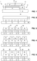
- Fig. 1 illustrates a III-nitride LED that may be used in example embodiments of the device. Any suitable semiconductor light emitting device may be used and embodiments of the invention are not limited to the device illustrated in Fig. 1 .
- the device of Fig. 1 is formed by growing a III-nitride semiconductor structure 12 on a growth substrate 10 as is known in the art.
- the growth substrate is often sapphire but may be any suitable substrate such as, for example, SiC, Si, GaN, or a composite substrate.
- a surface of the growth substrate on which the III-nitride semiconductor structure is grown may be patterned, roughened, or textured before growth, which may improve light extraction from the device.
- a surface of the growth substrate opposite the growth surface i.e. the surface through which a majority of light is extracted in a flip chip configuration
- the semiconductor structure includes a light emitting or active region sandwiched between n- and p-type regions.
- An n-type region 16 may be grown first and may include multiple layers of different compositions and dopant concentration including, for example, preparation layers such as buffer layers or nucleation layers, which may be n-type or not intentionally doped, and n- or even p-type device layers designed for particular optical, material, or electrical properties desirable for the light emitting region to efficiently emit light.
- a light emitting or active region 18 is grown over the n-type region. Examples of suitable light emitting regions include a single thick or thin light emitting layer, or a multiple quantum well light emitting region including multiple thin or thick light emitting layers separated by barrier layers.
- a p-type region 20 may then be grown over the light emitting region.
- the p-type region may include multiple layers of different composition, thickness, and dopant concentration, including layers that are not intentionally doped, or n-type layers.
- a p-contact is formed on the surface of the p-type region.
- the p-contact 21 often includes multiple conductive layers such as a reflective metal and a guard metal which may prevent or reduce electromigration of the reflective metal.
- the reflective metal is often silver but any suitable material or materials may be used.
- a portion of the p-contact 21, the p-type region 20, and the active region 18 is removed to expose a portion of the n-type region 16 on which an n-contact 22 is formed.
- the n- and p-contacts 22 and 21 are electrically isolated from each other by a gap 25 which may be filled with a dielectric such as an oxide of silicon or any other suitable material.
- n-contact vias may be formed; the n- and p-contacts 22 and 21 are not limited to the arrangement illustrated in Fig. 1 .
- the n- and p-contacts may be redistributed to form bond pads with a dielectric/metal stack, as is known in the art.
- one or more interconnects 26 and 28 are formed on or electrically connected to the n- and p-contacts 22 and 21.
- Interconnect 26 is electrically connected to n-contact 22 in Fig. 1 .
- Interconnect 28 is electrically connected to p-contact 21.
- Interconnects 26 and 28 are electrically isolated from the n- and p-contacts 22 and 21 and from each other by dielectric layer 24 and gap 27.
- Interconnects 26 and 28 may be, for example, solder, stud bumps, gold layers, or any other suitable structure.
- Many individual LEDs are formed on a single wafer then diced from the wafer of devices.
- the semiconductor structure and the n- and p-contacts 22 and 21 of a wafer of LEDs are represented in the following figures by block 12.
- the interconnects 26 and 28 of a wafer of LEDs are represented by block 14.
- the substrate 10 may be thinned after growth of the semiconductor structure or after forming the individual devices as described above in reference to Fig. 1 . After thinning, the substrate may be at least 50 ⁇ m thick in some embodiments, no more than 150 ⁇ m thick in some embodiments, at least 80 ⁇ m thick in some embodiments and no more than 120 ⁇ m thick in some embodiments.
- Figs. 2, 3, 4, 5 , and 6 illustrate forming a device according to embodiments of the invention.
- Temporary carrier 30 may be any suitable material such as, for example, wafer handling tape.
- slots 32 are formed in the growth substrate 10. Slots 32 are no more than 50 ⁇ m wide (for example, at the top of a slot with an angled sidewall as illustrated in Fig. 3 ) in some embodiments. The slots are disposed in the region between LEDs where the structure will be cut, as described below, to separate the wafer into individual LEDs or groups of LEDs.
- the slots may be formed by any suitable technique including, for example, wet or dry etching, laser scribing, or mechanical cutting such as sawing with a diamond blade.
- the slots 32 may extend through the entire thickness of substrate 10, though they need not.
- the slots 32 may have angled sidewalls, as illustrated in Fig. 3 , though angled sidewalls are not required.
- wavelength converting members 34 are attached to the top of substrate 10, such that the wavelength converting members are aligned with individual LEDs or groups of LEDs.
- Wavelength converting members 34 are generally wavelength converting structures that are formed separately from the wafer of LEDs, then attached to the substrate 10. As such, wavelength converting members 34 are self-supporting structures, not structures that are formed in situ on the substrate 10. Examples of suitable wavelength converting members 34 include phosphor that is formed into ceramic platelets, for example by sintering, and/or a phosphor or other wavelength converting material disposed in a transparent material, such as glass, silicone, or epoxy, that is cast or otherwise formed into a sheet, then cut into individual wavelength converting members 34.
- the wavelength converting material in wavelength converting members 34 may be, for example, conventional phosphors, organic phosphors, quantum dots, organic semiconductors, II-VI or III-V semiconductors, II-VI or III-V semiconductor quantum dots or nanocrystals, dyes, polymers, or other materials that luminesce.
- the wavelength converting material absorbs light emitted by the LED and emits light of one or more different wavelengths. Unconverted light emitted by the LED is often part of the final spectrum of light extracted from the structure, though it need not be.
- Examples of common combinations include a blue-emitting LED combined with a yellow-emitting wavelength converting material, a blue-emitting LED combined with green- and red-emitting wavelength converting materials, a UV-emitting LED combined with blue- and yellow-emitting wavelength converting materials, and a UV-emitting LED combined with blue-, green-, and red-emitting wavelength converting materials.
- Wavelength converting materials emitting other colors of light may be added to tailor the spectrum of light emitted from the structure.
- Wavelength converting member 34 may be attached to substrate 10 by, for example, gluing with a material such as silicone or any other suitable adhesive, direct bonding, or any other suitable technique.
- a reflective material 36 is disposed in the slots 32 formed in Fig. 3 .
- Reflective material may be, for example, reflective or other particles disposed in a transparent material.
- the particles and transparent material may be selected to have substantially different indices of refraction in order to cause optical scattering.
- the transparent material has a low index (for example, silicone may have an index of refraction of 1.4 or less) and the particles have a higher index (for example, TiO 2 has an index of refraction of 2.6).
- Any suitable reflective particle may be used, including, for example, TiO 2 , ZnO, or Al 2 O 3 .
- suitable transparent materials include silicone molding compound, liquid silicone, epoxy, and glass.
- the reflective particles, the transparent material, and/or the combination of reflective particles and transparent material has a higher thermal conductivity than common silicone materials. Common silicone materials typically have a thermal conductivity around 0.1-0.2W/mK.
- Reflective material 36 may be disposed in the slots 32 by any suitable technique such as, for example, dispensing or molding. Reflective material 36 may completely fill slots 32, as illustrated in Fig. 5 , such that the top of the reflective material 36 is coplanar with the tops of wavelength converting members 34 in some embodiments. Reflective material 36 does not completely fill slots 32 in some embodiments. In some embodiments, excessive reflective material 36 is removed after disposing the reflective material 36 in the slots. For example, reflective material that extends above the tops of slots 32, or that covers the LEDs, may be removed by any suitable technique, such as mechanical abrasion, grinding, or microbead blasting.
- individual LEDs are separated from the wafer by cutting through the reflective material 36 and the LED wafer in the regions 38 between LEDs.
- Individual LEDs may be cut from the wafer by any suitable technique including, for example, diamond sawing, laser cutting, or scribing and breaking.
- the kerf formed by cutting may be, for example, no more than 20 ⁇ m wide.
- the necessary thickness of reflective material 36 remaining on the sides of the LEDs in Fig. 6 after cutting, for proper functioning of the reflective material may depend on the type of reflective material. For reflective metal films, no more than 1 ⁇ m is required in some embodiments.
- diffuse reflectors such as TiO 2 in silicone, the reflectivity may depend on the thickness. For example, a diffuse reflector that is at least 90% reflective may be 20 ⁇ m thick or less in some embodiments and a diffuse reflector that is at least 95% reflective may be 50 ⁇ m thick or less in some embodiments.
- the finished LEDs are removed from the temporary carrier 30 by any suitable technique such as, for example, thermal release, transfer to a different carrier, or direct picking.
- Figs. 7, 8, and 9 illustrate an alternative embodiment, where individual LEDs are first separated from a wafer, then rearranged with larger pitch on a temporary carrier.
- a carrier 30 which may be a temporary carrier such as those described above in reference to Fig. 2 .
- the LEDs may be spaced at least 100 ⁇ m apart in some embodiments, no more than 800 ⁇ m apart in some embodiments, at least 400 ⁇ m apart in some embodiments, and no more than 600 ⁇ m apart in some embodiments.
- the growth substrate 10 on each LED may have substantially vertical sidewalls, rather than the angled sidewalls illustrated in the embodiment described in Figs. 2-6 , though vertical sidewalls are not required and the shape of the sidewall may depend on the technique used to separate the LEDs.
- wavelength converting elements 34 are attached to the growth substrate 10 of each LED, as described above in reference to Fig. 4 .
- reflective material 36 is disposed in the gaps between the LEDs, as described above in reference to Fig. 5 .
- the individual devices may be separated by cutting the reflective material, as described above in reference to Fig. 6 , then removed from the temporary carrier, as described above in reference to Fig. 6 .
- Figs. 10 and 11 illustrate an alternative embodiment where individual LEDs are first separated from a growth wafer, then disposed on a temporary carrier.
- individual LEDs are placed on a carrier 30 (as illustrated in Fig. 7 ), which may be a temporary carrier such as those described above in reference to Fig. 2 .
- Reflective material 36 is disposed in the regions between the LEDs, as described above in reference to Fig. 5 .
- a wavelength converting layer 40 is formed over the LEDs and the reflective material 36.
- Wavelength converting layer 40 may be, for example, a phosphor disposed in a transparent material such as silicone.
- Wavelength converting layer 40 may be formed by any suitable technique including, for example, lamination, molding, dispensing, spray coating, or spin coating.
- the LEDs are then separated by cutting through the structure, for example in regions 38 between neighboring LEDs, as described above in reference to Fig. 6 .
- the LEDs are then removed from the temporary carrier 30, as described above in reference to Fig. 6 .
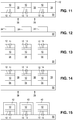
- Figs. 12, 13, and 14 illustrate an alternative embodiment.
- individual wavelength converting elements 34 are placed on a carrier 30, which may be a temporary carrier such as those described above in reference to Fig. 2 .
- the wavelength converting elements 34 are described above in reference to Fig. 4 .
- LEDs are attached to the wavelength converting elements 34.
- the LEDs may be attached using the methods and materials described above in reference to Fig 4 .
- a reflective material 36 is disposed in the regions between the LEDs, as described above in reference to Fig. 5 .
- the LEDs are then separated by cutting through the structure, for example in regions 38 between neighboring LEDs, as described above in reference to Fig. 6 .
- the LEDs are then removed from the temporary carrier 30, as described above in reference to Fig. 6 .
- Figs. 15 and 16 illustrate an alternative embodiment.
- LEDs are attached to a temporary carrier 30, which may be a temporary carrier such as those described above in reference to Fig. 2 .
- a temporary carrier such as those described above in reference to Fig. 2 .
- the tops of the LEDs in some embodiments, and the tops and sides of the LEDs in some embodiments are covered with a wavelength converting layer 42.
- the wavelength converting layer 42 may be, for example, a wavelength converting material mixed with a transparent material, and may be formed by any suitable technique, including, for example, lamination, molding, or electrophoretic deposition.
- a reflective material 36 is disposed in the regions between the LEDs, as described above in reference to Fig. 5 .
- the reflective material 36 may be formed by a technique that limits damage to the substantially conformal wavelength converting layer 42.
- One example of a suitable technique is dispensing reflective particles mixed with liquid silicone in the areas between the LEDs, then curing the liquid silicone.
- the LEDs are then separated by cutting through the structure, for example in regions 38 between neighboring LEDs, as described above in reference to Fig. 6 .
- the LEDs are then removed from the temporary carrier 30, as described above in reference to Fig. 6 .
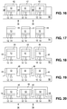
- Figs. 17, 18, 19, and 20 illustrate an alternative embodiment.
- LEDs are attached to a temporary carrier 30, which may be a temporary carrier such as those described above in reference to Fig. 2 .
- a temporary carrier such as those described above in reference to Fig. 2 .
- the tops of the LEDs are covered with a masking layer 44.
- the masking layer is applied to the growth substrate of a wafer of LEDs, before singulating the LEDs by cutting the growth substrate.
- the masking layer 44 may be, for example, photoresist, dielectric material, or any other suitable material.
- Masking layer 44 may be formed by any suitable technique, including, for example, spin-coating, roller-coating, dip-coating, lamination, spray-coating, evaporation, sputtering, and direct pick and place of a piece part such as a piece of glass.
- the masking layer 44 is patterned, for example, by photolithography, shadow masking, and/or wet or dry chemical etching.
- a reflective coating 46 is disposed over the structure illustrated in Fig. 17 .
- the reflective coating 46 may be any suitable material including, for example, a dichroic mirror, a distributed Bragg reflector (DBR), metallic film, or other suitable dielectric stack.
- the reflective coating 46 may be formed by any suitable technique including, for example, physical vapor deposition, CVD, sputtering, evaporation, and spray-coating.
- the reflective coating 46 may substantially conformally coat the structure, as illustrated in Fig. 18 , though this is not required.
- the masking layer 44 and the reflective coating 46 over the tops of the LEDs are removed by any suitable process such as, for example, a lift-off process. After removing the masking layer 44, reflective coating 46 remains on the sidewalls of the LEDs and the regions between the LEDs.
- Wavelength converting layer 48 is formed over the structure illustrated in Fig. 19 .
- Wavelength converting layer 48 may be, for example, a wavelength converting material mixed with a transparent material, and may be formed by any suitable technique including, for example, lamination, molding, spray coating, or spin coating.
- Wavelength converting layer 48 may fill the regions between the LEDs, as illustrated in Fig. 20 , or wavelength converting layer 48 may be a substantially conformal layer.
- the LEDs are then separated by cutting through the structure, for example in regions 38 between neighboring LEDs, as described above in reference to Fig. 6 .
- the LEDs are then removed from the temporary carrier 30, as described above in reference to Fig. 6 .
- a lens or other optical element is formed over the finished LED, which may be any of the devices described above.
- the sidewalls of the growth substrate may be angled.
Landscapes
- Engineering & Computer Science (AREA)
- Power Engineering (AREA)
- Microelectronics & Electronic Packaging (AREA)
- Physics & Mathematics (AREA)
- Condensed Matter Physics & Semiconductors (AREA)
- General Physics & Mathematics (AREA)
- Computer Hardware Design (AREA)
- Led Device Packages (AREA)
- Led Devices (AREA)
Applications Claiming Priority (3)
| Application Number | Priority Date | Filing Date | Title |
|---|---|---|---|
| US201361810833P | 2013-04-11 | 2013-04-11 | |
| US201361900466P | 2013-11-06 | 2013-11-06 | |
| PCT/IB2014/060310 WO2014167455A2 (en) | 2013-04-11 | 2014-03-31 | Top emitting semiconductor light emitting device |
Publications (2)
| Publication Number | Publication Date |
|---|---|
| EP2984685A2 EP2984685A2 (en) | 2016-02-17 |
| EP2984685B1 true EP2984685B1 (en) | 2018-12-19 |
Family
ID=51690078
Family Applications (1)
| Application Number | Title | Priority Date | Filing Date |
|---|---|---|---|
| EP14716970.0A Active EP2984685B1 (en) | 2013-04-11 | 2014-03-31 | Fabrication method for top emitting semiconductor light emitting devices |
Country Status (7)
| Country | Link |
|---|---|
| US (1) | US9871167B2 (enExample) |
| EP (1) | EP2984685B1 (enExample) |
| JP (2) | JP6680670B2 (enExample) |
| KR (1) | KR102245056B1 (enExample) |
| CN (3) | CN105378950A (enExample) |
| TW (1) | TWI659551B (enExample) |
| WO (1) | WO2014167455A2 (enExample) |
Families Citing this family (29)
| Publication number | Priority date | Publication date | Assignee | Title |
|---|---|---|---|---|
| JP7068771B2 (ja) * | 2013-07-08 | 2022-05-17 | ルミレッズ ホールディング ベーフェー | 波長変換式半導体発光デバイス |
| CN113658943A (zh) | 2013-12-13 | 2021-11-16 | 晶元光电股份有限公司 | 发光装置及其制作方法 |
| DE102014101492A1 (de) * | 2014-02-06 | 2015-08-06 | Osram Opto Semiconductors Gmbh | Optoelektronisches Halbleiterbauelement |
| US20160225962A1 (en) * | 2015-01-30 | 2016-08-04 | Empire Technology Development Llc | Nanoparticle gradient refractive index encapsulants for semi-conductor diodes |
| JP6832282B2 (ja) * | 2015-02-18 | 2021-02-24 | ルミレッズ ホールディング ベーフェー | 複数の積み重ねられた発光デバイスを有するデバイス |
| DE102015107593A1 (de) * | 2015-05-13 | 2016-11-17 | Osram Opto Semiconductors Gmbh | Optoelektronischer Halbleiterchip und Leuchtmittel |
| WO2017023502A1 (en) * | 2015-08-03 | 2017-02-09 | Koninklijke Philips N.V. | Semiconductor light emitting device with reflective side coating |
| US9753277B2 (en) | 2015-08-11 | 2017-09-05 | Delta Electronics, Inc. | Wavelength conversion device |
| JP6327220B2 (ja) * | 2015-08-31 | 2018-05-23 | 日亜化学工業株式会社 | 発光装置 |
| WO2017052800A1 (en) * | 2015-09-25 | 2017-03-30 | Koninklijke Philips N.V. | Surface emitter with light-emitting area equal to the led top surface and its fabrication |
| TWI587543B (zh) * | 2015-12-15 | 2017-06-11 | 李乃義 | 發光二極體封裝結構及其製造方法 |
| EP3398211B1 (en) * | 2015-12-29 | 2020-07-29 | Lumileds Holding B.V. | Flip chip led with side reflectors and phosphor |
| JP6974324B2 (ja) * | 2015-12-29 | 2021-12-01 | ルミレッズ ホールディング ベーフェー | 側面反射器と蛍光体とを備えるフリップチップled |
| FR3056014B1 (fr) * | 2016-09-15 | 2020-05-29 | Valeo Vision | Procede pour creer une isolation optique entre des pixels d'une matrice de sources lumineuses semi-conductrices |
| FR3061358B1 (fr) * | 2016-12-27 | 2021-06-11 | Aledia | Procede de fabrication d’un dispositif optoelectronique comportant des plots photoluminescents de photoresine |
| JP6699580B2 (ja) | 2017-02-09 | 2020-05-27 | 日亜化学工業株式会社 | 発光装置 |
| JP6662322B2 (ja) | 2017-02-09 | 2020-03-11 | 日亜化学工業株式会社 | 発光装置 |
| US10546985B2 (en) * | 2017-03-28 | 2020-01-28 | Nanosys, Inc. | Method for increasing the light output of microLED devices using quantum dots |
| US10224358B2 (en) * | 2017-05-09 | 2019-03-05 | Lumileds Llc | Light emitting device with reflective sidewall |
| JP6699634B2 (ja) | 2017-07-28 | 2020-05-27 | 日亜化学工業株式会社 | 発光装置の製造方法 |
| US11355548B2 (en) | 2017-12-20 | 2022-06-07 | Lumileds Llc | Monolithic segmented LED array architecture |
| US20190198564A1 (en) * | 2017-12-20 | 2019-06-27 | Lumileds Llc | Monolithic segmented led array architecture with islanded epitaxial growth |
| US10854794B2 (en) * | 2017-12-20 | 2020-12-01 | Lumileds Llc | Monolithic LED array structure |
| US11296262B2 (en) * | 2017-12-21 | 2022-04-05 | Lumileds Llc | Monolithic segmented LED array architecture with reduced area phosphor emission surface |
| US20190198720A1 (en) * | 2017-12-22 | 2019-06-27 | Lumileds Llc | Particle systems and patterning for monolithic led arrays |
| US11201267B2 (en) * | 2018-12-21 | 2021-12-14 | Lumileds Llc | Photoresist patterning process supporting two step phosphor-deposition to form an LED matrix array |
| US20240213401A1 (en) * | 2022-12-21 | 2024-06-27 | Creeled, Inc. | Textured lumiphore layer to improve light extraction for light-emitting diode chips and related methods |
| CN118899327A (zh) * | 2023-05-05 | 2024-11-05 | 北京字跳网络技术有限公司 | Micro/Nano LED装置及其制备方法 |
| CN117558851A (zh) * | 2024-01-05 | 2024-02-13 | 晶能光电股份有限公司 | 发光装置及其制备方法、发光阵列结构 |
Family Cites Families (43)
| Publication number | Priority date | Publication date | Assignee | Title |
|---|---|---|---|---|
| US6229160B1 (en) * | 1997-06-03 | 2001-05-08 | Lumileds Lighting, U.S., Llc | Light extraction from a semiconductor light-emitting device via chip shaping |
| US6650044B1 (en) * | 2000-10-13 | 2003-11-18 | Lumileds Lighting U.S., Llc | Stenciling phosphor layers on light emitting diodes |
| AU2002239288A1 (en) * | 2000-11-17 | 2002-05-27 | Emcore Corporation | Laser separated die with tapered sidewalls for improved light extraction |
| US6417019B1 (en) * | 2001-04-04 | 2002-07-09 | Lumileds Lighting, U.S., Llc | Phosphor converted light emitting diode |
| JP4143732B2 (ja) * | 2002-10-16 | 2008-09-03 | スタンレー電気株式会社 | 車載用波長変換素子 |
| US7361938B2 (en) * | 2004-06-03 | 2008-04-22 | Philips Lumileds Lighting Company Llc | Luminescent ceramic for a light emitting device |
| US20070228947A1 (en) * | 2004-10-13 | 2007-10-04 | Matsushita Electric Industrial Co., Ltd. | Luminescent Light Source, Method for Manufacturing the Same, and Light-Emitting Apparatus |
| US7964884B2 (en) | 2004-10-22 | 2011-06-21 | Seoul Opto Device Co., Ltd. | GaN compound semiconductor light emitting element and method of manufacturing the same |
| DE102004053116A1 (de) * | 2004-11-03 | 2006-05-04 | Tridonic Optoelectronics Gmbh | Leuchtdioden-Anordnung mit Farbkonversions-Material |
| CN100486397C (zh) * | 2005-04-19 | 2009-05-06 | 皇家飞利浦电子股份有限公司 | 包括红色发射陶瓷发光转换器的照明系统 |
| JP2007266343A (ja) | 2006-03-29 | 2007-10-11 | Toyoda Gosei Co Ltd | 発光装置 |
| CN101127379A (zh) * | 2006-08-16 | 2008-02-20 | 苏忠杰 | 高提取效率发光装置 |
| JP4650378B2 (ja) * | 2006-08-31 | 2011-03-16 | 日亜化学工業株式会社 | 発光装置の製造方法 |
| US20090275157A1 (en) * | 2006-10-02 | 2009-11-05 | Illumitex, Inc. | Optical device shaping |
| US8087960B2 (en) * | 2006-10-02 | 2012-01-03 | Illumitex, Inc. | LED system and method |
| KR101271225B1 (ko) | 2006-10-31 | 2013-06-03 | 삼성디스플레이 주식회사 | 발광 다이오드 칩 및 발광 다이오드 광원 모듈의 제조 방법 |
| JP4655029B2 (ja) * | 2006-11-20 | 2011-03-23 | パナソニック株式会社 | 発光装置および半導体発光素子の製造方法 |
| JP2008187030A (ja) * | 2007-01-30 | 2008-08-14 | Stanley Electric Co Ltd | 発光装置 |
| JP2008205229A (ja) * | 2007-02-21 | 2008-09-04 | Matsushita Electric Ind Co Ltd | 半導体発光素子、半導体発光装置および製造方法 |
| TWI350012B (en) * | 2007-05-04 | 2011-10-01 | Lite On Technology Corp | White light emitting diode and base thereof |
| US20090140279A1 (en) * | 2007-12-03 | 2009-06-04 | Goldeneye, Inc. | Substrate-free light emitting diode chip |
| KR100944008B1 (ko) * | 2007-12-17 | 2010-02-24 | 삼성전기주식회사 | 백색 발광소자 및 그 제조방법 |
| US8878219B2 (en) * | 2008-01-11 | 2014-11-04 | Cree, Inc. | Flip-chip phosphor coating method and devices fabricated utilizing method |
| US7923746B2 (en) * | 2008-03-12 | 2011-04-12 | Industrial Technology Research Institute | Light emitting diode package structure and method for fabricating the same |
| US20100279437A1 (en) * | 2009-05-01 | 2010-11-04 | Koninklijke Philips Electronics N.V. | Controlling edge emission in package-free led die |
| US8236582B2 (en) * | 2008-07-24 | 2012-08-07 | Philips Lumileds Lighting Company, Llc | Controlling edge emission in package-free LED die |
| WO2010035206A1 (en) * | 2008-09-25 | 2010-04-01 | Koninklijke Philips Electronics N.V. | Coated light emitting device and method for coating thereof |
| CN101551068A (zh) * | 2009-04-30 | 2009-10-07 | 旭丽电子(广州)有限公司 | 一种发光二极管装置及其封装方法 |
| US8440500B2 (en) * | 2009-05-20 | 2013-05-14 | Interlight Optotech Corporation | Light emitting device |
| JP2011066193A (ja) * | 2009-09-17 | 2011-03-31 | Rohm Co Ltd | 光学装置および光学装置の製造方法 |
| JP2011171327A (ja) * | 2010-02-16 | 2011-09-01 | Toshiba Corp | 発光素子およびその製造方法、並びに発光装置 |
| JP2012039013A (ja) * | 2010-08-10 | 2012-02-23 | Citizen Electronics Co Ltd | 発光装置の製造方法 |
| JP2012079776A (ja) * | 2010-09-30 | 2012-04-19 | Citizen Holdings Co Ltd | 半導体発光装置及びその製造方法 |
| JP2012084622A (ja) * | 2010-10-08 | 2012-04-26 | Citizen Holdings Co Ltd | 半導体発光素子の製造方法 |
| JP5508244B2 (ja) * | 2010-11-15 | 2014-05-28 | シチズンホールディングス株式会社 | 半導体発光装置の製造方法 |
| JP2012142410A (ja) * | 2010-12-28 | 2012-07-26 | Rohm Co Ltd | 発光素子ユニットおよびその製造方法、発光素子パッケージならびに照明装置 |
| JP5962102B2 (ja) * | 2011-03-24 | 2016-08-03 | 日亜化学工業株式会社 | 発光装置及びその製造方法 |
| JP5745319B2 (ja) * | 2011-04-14 | 2015-07-08 | 日東電工株式会社 | 蛍光反射シート、および、発光ダイオード装置の製造方法 |
| JP5670249B2 (ja) * | 2011-04-14 | 2015-02-18 | 日東電工株式会社 | 発光素子転写シートの製造方法、発光装置の製造方法、発光素子転写シートおよび発光装置 |
| JP5840377B2 (ja) * | 2011-04-14 | 2016-01-06 | 日東電工株式会社 | 反射樹脂シートおよび発光ダイオード装置の製造方法 |
| KR20140022019A (ko) * | 2011-04-20 | 2014-02-21 | 가부시키가이샤 에루므 | 발광장치 및 그 제조방법 |
| JP5619680B2 (ja) * | 2011-06-03 | 2014-11-05 | シチズンホールディングス株式会社 | 半導体発光素子の製造方法 |
| JP2013016588A (ja) * | 2011-07-01 | 2013-01-24 | Citizen Electronics Co Ltd | Led発光装置 |
-
2014
- 2014-03-31 JP JP2016507081A patent/JP6680670B2/ja active Active
- 2014-03-31 KR KR1020157032326A patent/KR102245056B1/ko active Active
- 2014-03-31 US US14/783,780 patent/US9871167B2/en active Active
- 2014-03-31 CN CN201480033532.3A patent/CN105378950A/zh active Pending
- 2014-03-31 EP EP14716970.0A patent/EP2984685B1/en active Active
- 2014-03-31 CN CN202010279869.XA patent/CN111613708B/zh active Active
- 2014-03-31 CN CN202010280757.6A patent/CN111628062A/zh active Pending
- 2014-03-31 WO PCT/IB2014/060310 patent/WO2014167455A2/en not_active Ceased
- 2014-04-11 TW TW103113487A patent/TWI659551B/zh active
-
2019
- 2019-08-09 JP JP2019147637A patent/JP6933691B2/ja active Active
Non-Patent Citations (1)
| Title |
|---|
| None * |
Also Published As
| Publication number | Publication date |
|---|---|
| WO2014167455A3 (en) | 2015-01-08 |
| CN111628062A (zh) | 2020-09-04 |
| CN111613708B (zh) | 2024-09-20 |
| KR102245056B1 (ko) | 2021-04-27 |
| US9871167B2 (en) | 2018-01-16 |
| WO2014167455A2 (en) | 2014-10-16 |
| US20160240735A1 (en) | 2016-08-18 |
| JP6933691B2 (ja) | 2021-09-08 |
| KR20150142033A (ko) | 2015-12-21 |
| JP2016518713A (ja) | 2016-06-23 |
| CN105378950A (zh) | 2016-03-02 |
| CN111613708A (zh) | 2020-09-01 |
| JP6680670B2 (ja) | 2020-04-15 |
| JP2019192946A (ja) | 2019-10-31 |
| EP2984685A2 (en) | 2016-02-17 |
| TW201501366A (zh) | 2015-01-01 |
| TWI659551B (zh) | 2019-05-11 |
Similar Documents
| Publication | Publication Date | Title |
|---|---|---|
| EP2984685B1 (en) | Fabrication method for top emitting semiconductor light emitting devices | |
| US11133442B2 (en) | Wavelength converted light emitting device with small source size | |
| EP2997610B1 (en) | Light emitting device with an optical element and a reflector | |
| EP2917938B1 (en) | Wavelength converted light emitting device | |
| EP3111487B1 (en) | Method of forming a wavelength converted light emitting device | |
| US20150280076A1 (en) | Light emitting device including a filter and a protective layer |
Legal Events
| Date | Code | Title | Description |
|---|---|---|---|
| PUAI | Public reference made under article 153(3) epc to a published international application that has entered the european phase |
Free format text: ORIGINAL CODE: 0009012 |
|
| 17P | Request for examination filed |
Effective date: 20151111 |
|
| AK | Designated contracting states |
Kind code of ref document: A2 Designated state(s): AL AT BE BG CH CY CZ DE DK EE ES FI FR GB GR HR HU IE IS IT LI LT LU LV MC MK MT NL NO PL PT RO RS SE SI SK SM TR |
|
| AX | Request for extension of the european patent |
Extension state: BA ME |
|
| DAX | Request for extension of the european patent (deleted) | ||
| STAA | Information on the status of an ep patent application or granted ep patent |
Free format text: STATUS: EXAMINATION IS IN PROGRESS |
|
| 17Q | First examination report despatched |
Effective date: 20170302 |
|
| GRAP | Despatch of communication of intention to grant a patent |
Free format text: ORIGINAL CODE: EPIDOSNIGR1 |
|
| STAA | Information on the status of an ep patent application or granted ep patent |
Free format text: STATUS: GRANT OF PATENT IS INTENDED |
|
| RAP1 | Party data changed (applicant data changed or rights of an application transferred) |
Owner name: LUMILEDS HOLDING B.V. |
|
| INTG | Intention to grant announced |
Effective date: 20180717 |
|
| GRAS | Grant fee paid |
Free format text: ORIGINAL CODE: EPIDOSNIGR3 |
|
| GRAA | (expected) grant |
Free format text: ORIGINAL CODE: 0009210 |
|
| STAA | Information on the status of an ep patent application or granted ep patent |
Free format text: STATUS: THE PATENT HAS BEEN GRANTED |
|
| AK | Designated contracting states |
Kind code of ref document: B1 Designated state(s): AL AT BE BG CH CY CZ DE DK EE ES FI FR GB GR HR HU IE IS IT LI LT LU LV MC MK MT NL NO PL PT RO RS SE SI SK SM TR |
|
| REG | Reference to a national code |
Ref country code: GB Ref legal event code: FG4D |
|
| REG | Reference to a national code |
Ref country code: CH Ref legal event code: EP |
|
| REG | Reference to a national code |
Ref country code: IE Ref legal event code: FG4D |
|
| REG | Reference to a national code |
Ref country code: DE Ref legal event code: R096 Ref document number: 602014038163 Country of ref document: DE |
|
| REG | Reference to a national code |
Ref country code: AT Ref legal event code: REF Ref document number: 1079610 Country of ref document: AT Kind code of ref document: T Effective date: 20190115 |
|
| RAP2 | Party data changed (patent owner data changed or rights of a patent transferred) |
Owner name: LUMILEDS HOLDING B.V. |
|
| REG | Reference to a national code |
Ref country code: NL Ref legal event code: MP Effective date: 20181219 |
|
| PG25 | Lapsed in a contracting state [announced via postgrant information from national office to epo] |
Ref country code: FI Free format text: LAPSE BECAUSE OF FAILURE TO SUBMIT A TRANSLATION OF THE DESCRIPTION OR TO PAY THE FEE WITHIN THE PRESCRIBED TIME-LIMIT Effective date: 20181219 Ref country code: BG Free format text: LAPSE BECAUSE OF FAILURE TO SUBMIT A TRANSLATION OF THE DESCRIPTION OR TO PAY THE FEE WITHIN THE PRESCRIBED TIME-LIMIT Effective date: 20190319 Ref country code: HR Free format text: LAPSE BECAUSE OF FAILURE TO SUBMIT A TRANSLATION OF THE DESCRIPTION OR TO PAY THE FEE WITHIN THE PRESCRIBED TIME-LIMIT Effective date: 20181219 Ref country code: LV Free format text: LAPSE BECAUSE OF FAILURE TO SUBMIT A TRANSLATION OF THE DESCRIPTION OR TO PAY THE FEE WITHIN THE PRESCRIBED TIME-LIMIT Effective date: 20181219 Ref country code: LT Free format text: LAPSE BECAUSE OF FAILURE TO SUBMIT A TRANSLATION OF THE DESCRIPTION OR TO PAY THE FEE WITHIN THE PRESCRIBED TIME-LIMIT Effective date: 20181219 Ref country code: NO Free format text: LAPSE BECAUSE OF FAILURE TO SUBMIT A TRANSLATION OF THE DESCRIPTION OR TO PAY THE FEE WITHIN THE PRESCRIBED TIME-LIMIT Effective date: 20190319 |
|
| REG | Reference to a national code |
Ref country code: LT Ref legal event code: MG4D |
|
| REG | Reference to a national code |
Ref country code: AT Ref legal event code: MK05 Ref document number: 1079610 Country of ref document: AT Kind code of ref document: T Effective date: 20181219 |
|
| PG25 | Lapsed in a contracting state [announced via postgrant information from national office to epo] |
Ref country code: AL Free format text: LAPSE BECAUSE OF FAILURE TO SUBMIT A TRANSLATION OF THE DESCRIPTION OR TO PAY THE FEE WITHIN THE PRESCRIBED TIME-LIMIT Effective date: 20181219 Ref country code: RS Free format text: LAPSE BECAUSE OF FAILURE TO SUBMIT A TRANSLATION OF THE DESCRIPTION OR TO PAY THE FEE WITHIN THE PRESCRIBED TIME-LIMIT Effective date: 20181219 Ref country code: SE Free format text: LAPSE BECAUSE OF FAILURE TO SUBMIT A TRANSLATION OF THE DESCRIPTION OR TO PAY THE FEE WITHIN THE PRESCRIBED TIME-LIMIT Effective date: 20181219 Ref country code: GR Free format text: LAPSE BECAUSE OF FAILURE TO SUBMIT A TRANSLATION OF THE DESCRIPTION OR TO PAY THE FEE WITHIN THE PRESCRIBED TIME-LIMIT Effective date: 20190320 |
|
| PG25 | Lapsed in a contracting state [announced via postgrant information from national office to epo] |
Ref country code: NL Free format text: LAPSE BECAUSE OF FAILURE TO SUBMIT A TRANSLATION OF THE DESCRIPTION OR TO PAY THE FEE WITHIN THE PRESCRIBED TIME-LIMIT Effective date: 20181219 |
|
| PG25 | Lapsed in a contracting state [announced via postgrant information from national office to epo] |
Ref country code: IT Free format text: LAPSE BECAUSE OF FAILURE TO SUBMIT A TRANSLATION OF THE DESCRIPTION OR TO PAY THE FEE WITHIN THE PRESCRIBED TIME-LIMIT Effective date: 20181219 Ref country code: CZ Free format text: LAPSE BECAUSE OF FAILURE TO SUBMIT A TRANSLATION OF THE DESCRIPTION OR TO PAY THE FEE WITHIN THE PRESCRIBED TIME-LIMIT Effective date: 20181219 Ref country code: PT Free format text: LAPSE BECAUSE OF FAILURE TO SUBMIT A TRANSLATION OF THE DESCRIPTION OR TO PAY THE FEE WITHIN THE PRESCRIBED TIME-LIMIT Effective date: 20190419 Ref country code: ES Free format text: LAPSE BECAUSE OF FAILURE TO SUBMIT A TRANSLATION OF THE DESCRIPTION OR TO PAY THE FEE WITHIN THE PRESCRIBED TIME-LIMIT Effective date: 20181219 Ref country code: PL Free format text: LAPSE BECAUSE OF FAILURE TO SUBMIT A TRANSLATION OF THE DESCRIPTION OR TO PAY THE FEE WITHIN THE PRESCRIBED TIME-LIMIT Effective date: 20181219 |
|
| PG25 | Lapsed in a contracting state [announced via postgrant information from national office to epo] |
Ref country code: SK Free format text: LAPSE BECAUSE OF FAILURE TO SUBMIT A TRANSLATION OF THE DESCRIPTION OR TO PAY THE FEE WITHIN THE PRESCRIBED TIME-LIMIT Effective date: 20181219 Ref country code: RO Free format text: LAPSE BECAUSE OF FAILURE TO SUBMIT A TRANSLATION OF THE DESCRIPTION OR TO PAY THE FEE WITHIN THE PRESCRIBED TIME-LIMIT Effective date: 20181219 Ref country code: IS Free format text: LAPSE BECAUSE OF FAILURE TO SUBMIT A TRANSLATION OF THE DESCRIPTION OR TO PAY THE FEE WITHIN THE PRESCRIBED TIME-LIMIT Effective date: 20190419 Ref country code: SM Free format text: LAPSE BECAUSE OF FAILURE TO SUBMIT A TRANSLATION OF THE DESCRIPTION OR TO PAY THE FEE WITHIN THE PRESCRIBED TIME-LIMIT Effective date: 20181219 Ref country code: EE Free format text: LAPSE BECAUSE OF FAILURE TO SUBMIT A TRANSLATION OF THE DESCRIPTION OR TO PAY THE FEE WITHIN THE PRESCRIBED TIME-LIMIT Effective date: 20181219 |
|
| REG | Reference to a national code |
Ref country code: DE Ref legal event code: R097 Ref document number: 602014038163 Country of ref document: DE |
|
| PLBE | No opposition filed within time limit |
Free format text: ORIGINAL CODE: 0009261 |
|
| STAA | Information on the status of an ep patent application or granted ep patent |
Free format text: STATUS: NO OPPOSITION FILED WITHIN TIME LIMIT |
|
| PG25 | Lapsed in a contracting state [announced via postgrant information from national office to epo] |
Ref country code: AT Free format text: LAPSE BECAUSE OF FAILURE TO SUBMIT A TRANSLATION OF THE DESCRIPTION OR TO PAY THE FEE WITHIN THE PRESCRIBED TIME-LIMIT Effective date: 20181219 Ref country code: MC Free format text: LAPSE BECAUSE OF FAILURE TO SUBMIT A TRANSLATION OF THE DESCRIPTION OR TO PAY THE FEE WITHIN THE PRESCRIBED TIME-LIMIT Effective date: 20181219 Ref country code: DK Free format text: LAPSE BECAUSE OF FAILURE TO SUBMIT A TRANSLATION OF THE DESCRIPTION OR TO PAY THE FEE WITHIN THE PRESCRIBED TIME-LIMIT Effective date: 20181219 |
|
| REG | Reference to a national code |
Ref country code: CH Ref legal event code: PL |
|
| 26N | No opposition filed |
Effective date: 20190920 |
|
| PG25 | Lapsed in a contracting state [announced via postgrant information from national office to epo] |
Ref country code: LU Free format text: LAPSE BECAUSE OF NON-PAYMENT OF DUE FEES Effective date: 20190331 |
|
| REG | Reference to a national code |
Ref country code: BE Ref legal event code: MM Effective date: 20190331 |
|
| PG25 | Lapsed in a contracting state [announced via postgrant information from national office to epo] |
Ref country code: IE Free format text: LAPSE BECAUSE OF NON-PAYMENT OF DUE FEES Effective date: 20190331 Ref country code: CH Free format text: LAPSE BECAUSE OF NON-PAYMENT OF DUE FEES Effective date: 20190331 Ref country code: LI Free format text: LAPSE BECAUSE OF NON-PAYMENT OF DUE FEES Effective date: 20190331 |
|
| PG25 | Lapsed in a contracting state [announced via postgrant information from national office to epo] |
Ref country code: SI Free format text: LAPSE BECAUSE OF FAILURE TO SUBMIT A TRANSLATION OF THE DESCRIPTION OR TO PAY THE FEE WITHIN THE PRESCRIBED TIME-LIMIT Effective date: 20181219 Ref country code: BE Free format text: LAPSE BECAUSE OF NON-PAYMENT OF DUE FEES Effective date: 20190331 |
|
| PG25 | Lapsed in a contracting state [announced via postgrant information from national office to epo] |
Ref country code: TR Free format text: LAPSE BECAUSE OF FAILURE TO SUBMIT A TRANSLATION OF THE DESCRIPTION OR TO PAY THE FEE WITHIN THE PRESCRIBED TIME-LIMIT Effective date: 20181219 |
|
| PG25 | Lapsed in a contracting state [announced via postgrant information from national office to epo] |
Ref country code: MT Free format text: LAPSE BECAUSE OF NON-PAYMENT OF DUE FEES Effective date: 20190331 |
|
| PG25 | Lapsed in a contracting state [announced via postgrant information from national office to epo] |
Ref country code: CY Free format text: LAPSE BECAUSE OF FAILURE TO SUBMIT A TRANSLATION OF THE DESCRIPTION OR TO PAY THE FEE WITHIN THE PRESCRIBED TIME-LIMIT Effective date: 20181219 |
|
| PG25 | Lapsed in a contracting state [announced via postgrant information from national office to epo] |
Ref country code: HU Free format text: LAPSE BECAUSE OF FAILURE TO SUBMIT A TRANSLATION OF THE DESCRIPTION OR TO PAY THE FEE WITHIN THE PRESCRIBED TIME-LIMIT; INVALID AB INITIO Effective date: 20140331 |
|
| PG25 | Lapsed in a contracting state [announced via postgrant information from national office to epo] |
Ref country code: MK Free format text: LAPSE BECAUSE OF FAILURE TO SUBMIT A TRANSLATION OF THE DESCRIPTION OR TO PAY THE FEE WITHIN THE PRESCRIBED TIME-LIMIT Effective date: 20181219 |
|
| P01 | Opt-out of the competence of the unified patent court (upc) registered |
Effective date: 20230530 |
|
| REG | Reference to a national code |
Ref country code: DE Ref legal event code: R079 Ref document number: 602014038163 Country of ref document: DE Free format text: PREVIOUS MAIN CLASS: H01L0033200000 Ipc: H10H0020819000 |
|
| PGFP | Annual fee paid to national office [announced via postgrant information from national office to epo] |
Ref country code: DE Payment date: 20250327 Year of fee payment: 12 |
|
| PGFP | Annual fee paid to national office [announced via postgrant information from national office to epo] |
Ref country code: FR Payment date: 20250324 Year of fee payment: 12 |
|
| PGFP | Annual fee paid to national office [announced via postgrant information from national office to epo] |
Ref country code: GB Payment date: 20250325 Year of fee payment: 12 |