EP2981993B1 - Organic compound and organic light-emitting device - Google Patents
Organic compound and organic light-emitting device Download PDFInfo
- Publication number
- EP2981993B1 EP2981993B1 EP14778819.4A EP14778819A EP2981993B1 EP 2981993 B1 EP2981993 B1 EP 2981993B1 EP 14778819 A EP14778819 A EP 14778819A EP 2981993 B1 EP2981993 B1 EP 2981993B1
- Authority
- EP
- European Patent Office
- Prior art keywords
- group
- compound
- organic light
- emitting device
- organic
- Prior art date
- Legal status (The legal status is an assumption and is not a legal conclusion. Google has not performed a legal analysis and makes no representation as to the accuracy of the status listed.)
- Active
Links
Images
Classifications
-
- H—ELECTRICITY
- H10—SEMICONDUCTOR DEVICES; ELECTRIC SOLID-STATE DEVICES NOT OTHERWISE PROVIDED FOR
- H10K—ORGANIC ELECTRIC SOLID-STATE DEVICES
- H10K85/00—Organic materials used in the body or electrodes of devices covered by this subclass
- H10K85/60—Organic compounds having low molecular weight
- H10K85/615—Polycyclic condensed aromatic hydrocarbons, e.g. anthracene
- H10K85/626—Polycyclic condensed aromatic hydrocarbons, e.g. anthracene containing more than one polycyclic condensed aromatic rings, e.g. bis-anthracene
-
- C—CHEMISTRY; METALLURGY
- C07—ORGANIC CHEMISTRY
- C07C—ACYCLIC OR CARBOCYCLIC COMPOUNDS
- C07C13/00—Cyclic hydrocarbons containing rings other than, or in addition to, six-membered aromatic rings
- C07C13/28—Polycyclic hydrocarbons or acyclic hydrocarbon derivatives thereof
- C07C13/32—Polycyclic hydrocarbons or acyclic hydrocarbon derivatives thereof with condensed rings
- C07C13/54—Polycyclic hydrocarbons or acyclic hydrocarbon derivatives thereof with condensed rings with three condensed rings
- C07C13/547—Polycyclic hydrocarbons or acyclic hydrocarbon derivatives thereof with condensed rings with three condensed rings at least one ring not being six-membered, the other rings being at the most six-membered
- C07C13/567—Polycyclic hydrocarbons or acyclic hydrocarbon derivatives thereof with condensed rings with three condensed rings at least one ring not being six-membered, the other rings being at the most six-membered with a fluorene or hydrogenated fluorene ring system
-
- C—CHEMISTRY; METALLURGY
- C07—ORGANIC CHEMISTRY
- C07C—ACYCLIC OR CARBOCYCLIC COMPOUNDS
- C07C13/00—Cyclic hydrocarbons containing rings other than, or in addition to, six-membered aromatic rings
- C07C13/28—Polycyclic hydrocarbons or acyclic hydrocarbon derivatives thereof
- C07C13/32—Polycyclic hydrocarbons or acyclic hydrocarbon derivatives thereof with condensed rings
- C07C13/54—Polycyclic hydrocarbons or acyclic hydrocarbon derivatives thereof with condensed rings with three condensed rings
- C07C13/605—Polycyclic hydrocarbons or acyclic hydrocarbon derivatives thereof with condensed rings with three condensed rings with a bridged ring system
- C07C13/615—Polycyclic hydrocarbons or acyclic hydrocarbon derivatives thereof with condensed rings with three condensed rings with a bridged ring system with an adamantane ring
-
- C—CHEMISTRY; METALLURGY
- C07—ORGANIC CHEMISTRY
- C07C—ACYCLIC OR CARBOCYCLIC COMPOUNDS
- C07C13/00—Cyclic hydrocarbons containing rings other than, or in addition to, six-membered aromatic rings
- C07C13/28—Polycyclic hydrocarbons or acyclic hydrocarbon derivatives thereof
- C07C13/32—Polycyclic hydrocarbons or acyclic hydrocarbon derivatives thereof with condensed rings
- C07C13/62—Polycyclic hydrocarbons or acyclic hydrocarbon derivatives thereof with condensed rings with more than three condensed rings
- C07C13/66—Polycyclic hydrocarbons or acyclic hydrocarbon derivatives thereof with condensed rings with more than three condensed rings the condensed ring system contains only four rings
-
- C—CHEMISTRY; METALLURGY
- C07—ORGANIC CHEMISTRY
- C07C—ACYCLIC OR CARBOCYCLIC COMPOUNDS
- C07C22/00—Cyclic compounds containing halogen atoms bound to an acyclic carbon atom
- C07C22/02—Cyclic compounds containing halogen atoms bound to an acyclic carbon atom having unsaturation in the rings
- C07C22/04—Cyclic compounds containing halogen atoms bound to an acyclic carbon atom having unsaturation in the rings containing six-membered aromatic rings
- C07C22/08—Cyclic compounds containing halogen atoms bound to an acyclic carbon atom having unsaturation in the rings containing six-membered aromatic rings containing fluorine
-
- C—CHEMISTRY; METALLURGY
- C07—ORGANIC CHEMISTRY
- C07C—ACYCLIC OR CARBOCYCLIC COMPOUNDS
- C07C25/00—Compounds containing at least one halogen atom bound to a six-membered aromatic ring
- C07C25/18—Polycyclic aromatic halogenated hydrocarbons
- C07C25/22—Polycyclic aromatic halogenated hydrocarbons with condensed rings
-
- C—CHEMISTRY; METALLURGY
- C07—ORGANIC CHEMISTRY
- C07C—ACYCLIC OR CARBOCYCLIC COMPOUNDS
- C07C43/00—Ethers; Compounds having groups, groups or groups
- C07C43/02—Ethers
- C07C43/257—Ethers having an ether-oxygen atom bound to carbon atoms both belonging to six-membered aromatic rings
- C07C43/275—Ethers having an ether-oxygen atom bound to carbon atoms both belonging to six-membered aromatic rings having all ether-oxygen atoms bound to carbon atoms of six-membered aromatic rings
-
- G—PHYSICS
- G03—PHOTOGRAPHY; CINEMATOGRAPHY; ANALOGOUS TECHNIQUES USING WAVES OTHER THAN OPTICAL WAVES; ELECTROGRAPHY; HOLOGRAPHY
- G03G—ELECTROGRAPHY; ELECTROPHOTOGRAPHY; MAGNETOGRAPHY
- G03G15/00—Apparatus for electrographic processes using a charge pattern
- G03G15/04—Apparatus for electrographic processes using a charge pattern for exposing, i.e. imagewise exposure by optically projecting the original image on a photoconductive recording material
- G03G15/04036—Details of illuminating systems, e.g. lamps, reflectors
- G03G15/04045—Details of illuminating systems, e.g. lamps, reflectors for exposing image information provided otherwise than by directly projecting the original image onto the photoconductive recording material, e.g. digital copiers
- G03G15/04063—Details of illuminating systems, e.g. lamps, reflectors for exposing image information provided otherwise than by directly projecting the original image onto the photoconductive recording material, e.g. digital copiers by EL-bars
-
- G—PHYSICS
- G06—COMPUTING OR CALCULATING; COUNTING
- G06F—ELECTRIC DIGITAL DATA PROCESSING
- G06F3/00—Input arrangements for transferring data to be processed into a form capable of being handled by the computer; Output arrangements for transferring data from processing unit to output unit, e.g. interface arrangements
- G06F3/01—Input arrangements or combined input and output arrangements for interaction between user and computer
- G06F3/03—Arrangements for converting the position or the displacement of a member into a coded form
- G06F3/041—Digitisers, e.g. for touch screens or touch pads, characterised by the transducing means
- G06F3/0412—Digitisers structurally integrated in a display
-
- H—ELECTRICITY
- H05—ELECTRIC TECHNIQUES NOT OTHERWISE PROVIDED FOR
- H05B—ELECTRIC HEATING; ELECTRIC LIGHT SOURCES NOT OTHERWISE PROVIDED FOR; CIRCUIT ARRANGEMENTS FOR ELECTRIC LIGHT SOURCES, IN GENERAL
- H05B45/00—Circuit arrangements for operating light-emitting diodes [LED]
- H05B45/60—Circuit arrangements for operating LEDs comprising organic material, e.g. for operating organic light-emitting diodes [OLED] or polymer light-emitting diodes [PLED]
-
- H—ELECTRICITY
- H10—SEMICONDUCTOR DEVICES; ELECTRIC SOLID-STATE DEVICES NOT OTHERWISE PROVIDED FOR
- H10K—ORGANIC ELECTRIC SOLID-STATE DEVICES
- H10K59/00—Integrated devices, or assemblies of multiple devices, comprising at least one organic light-emitting element covered by group H10K50/00
- H10K59/10—OLED displays
- H10K59/12—Active-matrix OLED [AMOLED] displays
- H10K59/123—Connection of the pixel electrodes to the thin film transistors [TFT]
-
- H—ELECTRICITY
- H10—SEMICONDUCTOR DEVICES; ELECTRIC SOLID-STATE DEVICES NOT OTHERWISE PROVIDED FOR
- H10K—ORGANIC ELECTRIC SOLID-STATE DEVICES
- H10K85/00—Organic materials used in the body or electrodes of devices covered by this subclass
- H10K85/60—Organic compounds having low molecular weight
- H10K85/615—Polycyclic condensed aromatic hydrocarbons, e.g. anthracene
- H10K85/622—Polycyclic condensed aromatic hydrocarbons, e.g. anthracene containing four rings, e.g. pyrene
-
- H—ELECTRICITY
- H10—SEMICONDUCTOR DEVICES; ELECTRIC SOLID-STATE DEVICES NOT OTHERWISE PROVIDED FOR
- H10K—ORGANIC ELECTRIC SOLID-STATE DEVICES
- H10K85/00—Organic materials used in the body or electrodes of devices covered by this subclass
- H10K85/60—Organic compounds having low molecular weight
- H10K85/615—Polycyclic condensed aromatic hydrocarbons, e.g. anthracene
- H10K85/623—Polycyclic condensed aromatic hydrocarbons, e.g. anthracene containing five rings, e.g. pentacene
-
- H—ELECTRICITY
- H10—SEMICONDUCTOR DEVICES; ELECTRIC SOLID-STATE DEVICES NOT OTHERWISE PROVIDED FOR
- H10K—ORGANIC ELECTRIC SOLID-STATE DEVICES
- H10K85/00—Organic materials used in the body or electrodes of devices covered by this subclass
- H10K85/60—Organic compounds having low molecular weight
- H10K85/631—Amine compounds having at least two aryl rest on at least one amine-nitrogen atom, e.g. triphenylamine
- H10K85/633—Amine compounds having at least two aryl rest on at least one amine-nitrogen atom, e.g. triphenylamine comprising polycyclic condensed aromatic hydrocarbons as substituents on the nitrogen atom
-
- H—ELECTRICITY
- H10—SEMICONDUCTOR DEVICES; ELECTRIC SOLID-STATE DEVICES NOT OTHERWISE PROVIDED FOR
- H10K—ORGANIC ELECTRIC SOLID-STATE DEVICES
- H10K85/00—Organic materials used in the body or electrodes of devices covered by this subclass
- H10K85/60—Organic compounds having low molecular weight
- H10K85/649—Aromatic compounds comprising a hetero atom
- H10K85/657—Polycyclic condensed heteroaromatic hydrocarbons
- H10K85/6572—Polycyclic condensed heteroaromatic hydrocarbons comprising only nitrogen in the heteroaromatic polycondensed ring system, e.g. phenanthroline or carbazole
-
- C—CHEMISTRY; METALLURGY
- C07—ORGANIC CHEMISTRY
- C07C—ACYCLIC OR CARBOCYCLIC COMPOUNDS
- C07C2601/00—Systems containing only non-condensed rings
- C07C2601/12—Systems containing only non-condensed rings with a six-membered ring
- C07C2601/14—The ring being saturated
-
- C—CHEMISTRY; METALLURGY
- C07—ORGANIC CHEMISTRY
- C07C—ACYCLIC OR CARBOCYCLIC COMPOUNDS
- C07C2603/00—Systems containing at least three condensed rings
- C07C2603/02—Ortho- or ortho- and peri-condensed systems
- C07C2603/04—Ortho- or ortho- and peri-condensed systems containing three rings
- C07C2603/06—Ortho- or ortho- and peri-condensed systems containing three rings containing at least one ring with less than six ring members
- C07C2603/10—Ortho- or ortho- and peri-condensed systems containing three rings containing at least one ring with less than six ring members containing five-membered rings
- C07C2603/12—Ortho- or ortho- and peri-condensed systems containing three rings containing at least one ring with less than six ring members containing five-membered rings only one five-membered ring
- C07C2603/18—Fluorenes; Hydrogenated fluorenes
-
- C—CHEMISTRY; METALLURGY
- C07—ORGANIC CHEMISTRY
- C07C—ACYCLIC OR CARBOCYCLIC COMPOUNDS
- C07C2603/00—Systems containing at least three condensed rings
- C07C2603/02—Ortho- or ortho- and peri-condensed systems
- C07C2603/04—Ortho- or ortho- and peri-condensed systems containing three rings
- C07C2603/22—Ortho- or ortho- and peri-condensed systems containing three rings containing only six-membered rings
- C07C2603/26—Phenanthrenes; Hydrogenated phenanthrenes
-
- C—CHEMISTRY; METALLURGY
- C07—ORGANIC CHEMISTRY
- C07C—ACYCLIC OR CARBOCYCLIC COMPOUNDS
- C07C2603/00—Systems containing at least three condensed rings
- C07C2603/02—Ortho- or ortho- and peri-condensed systems
- C07C2603/40—Ortho- or ortho- and peri-condensed systems containing four condensed rings
- C07C2603/42—Ortho- or ortho- and peri-condensed systems containing four condensed rings containing only six-membered rings
- C07C2603/48—Chrysenes; Hydrogenated chrysenes
-
- C—CHEMISTRY; METALLURGY
- C07—ORGANIC CHEMISTRY
- C07C—ACYCLIC OR CARBOCYCLIC COMPOUNDS
- C07C2603/00—Systems containing at least three condensed rings
- C07C2603/02—Ortho- or ortho- and peri-condensed systems
- C07C2603/40—Ortho- or ortho- and peri-condensed systems containing four condensed rings
- C07C2603/42—Ortho- or ortho- and peri-condensed systems containing four condensed rings containing only six-membered rings
- C07C2603/50—Pyrenes; Hydrogenated pyrenes
-
- C—CHEMISTRY; METALLURGY
- C07—ORGANIC CHEMISTRY
- C07C—ACYCLIC OR CARBOCYCLIC COMPOUNDS
- C07C2603/00—Systems containing at least three condensed rings
- C07C2603/56—Ring systems containing bridged rings
- C07C2603/58—Ring systems containing bridged rings containing three rings
- C07C2603/70—Ring systems containing bridged rings containing three rings containing only six-membered rings
- C07C2603/74—Adamantanes
-
- H—ELECTRICITY
- H10—SEMICONDUCTOR DEVICES; ELECTRIC SOLID-STATE DEVICES NOT OTHERWISE PROVIDED FOR
- H10K—ORGANIC ELECTRIC SOLID-STATE DEVICES
- H10K50/00—Organic light-emitting devices
- H10K50/10—OLEDs or polymer light-emitting diodes [PLED]
- H10K50/11—OLEDs or polymer light-emitting diodes [PLED] characterised by the electroluminescent [EL] layers
-
- H—ELECTRICITY
- H10—SEMICONDUCTOR DEVICES; ELECTRIC SOLID-STATE DEVICES NOT OTHERWISE PROVIDED FOR
- H10K—ORGANIC ELECTRIC SOLID-STATE DEVICES
- H10K50/00—Organic light-emitting devices
- H10K50/10—OLEDs or polymer light-emitting diodes [PLED]
- H10K50/14—Carrier transporting layers
- H10K50/15—Hole transporting layers
-
- H—ELECTRICITY
- H10—SEMICONDUCTOR DEVICES; ELECTRIC SOLID-STATE DEVICES NOT OTHERWISE PROVIDED FOR
- H10K—ORGANIC ELECTRIC SOLID-STATE DEVICES
- H10K50/00—Organic light-emitting devices
- H10K50/10—OLEDs or polymer light-emitting diodes [PLED]
- H10K50/14—Carrier transporting layers
- H10K50/16—Electron transporting layers
-
- H—ELECTRICITY
- H10—SEMICONDUCTOR DEVICES; ELECTRIC SOLID-STATE DEVICES NOT OTHERWISE PROVIDED FOR
- H10K—ORGANIC ELECTRIC SOLID-STATE DEVICES
- H10K85/00—Organic materials used in the body or electrodes of devices covered by this subclass
- H10K85/30—Coordination compounds
- H10K85/341—Transition metal complexes, e.g. Ru(II)polypyridine complexes
- H10K85/342—Transition metal complexes, e.g. Ru(II)polypyridine complexes comprising iridium
-
- H—ELECTRICITY
- H10—SEMICONDUCTOR DEVICES; ELECTRIC SOLID-STATE DEVICES NOT OTHERWISE PROVIDED FOR
- H10K—ORGANIC ELECTRIC SOLID-STATE DEVICES
- H10K85/00—Organic materials used in the body or electrodes of devices covered by this subclass
- H10K85/60—Organic compounds having low molecular weight
- H10K85/649—Aromatic compounds comprising a hetero atom
- H10K85/657—Polycyclic condensed heteroaromatic hydrocarbons
- H10K85/6576—Polycyclic condensed heteroaromatic hydrocarbons comprising only sulfur in the heteroaromatic polycondensed ring system, e.g. benzothiophene
Definitions
- the present invention relates to an organic compound and an organic light-emitting device using the compound.
- An organic light-emitting device is an electronic device including a pair of electrodes and an organic compound layer placed between the electrodes. An electron and a hole are injected from the pair of electrodes, the electron and the hole recombine in the organic compound layer to produce an exciton of a luminous organic compound, and the organic light-emitting device emits light when the exciton returns to its ground state.
- Patent Literature 1 proposes that an improvement in hole transport property be achieved by forming a hole transport layer from a mixture of different hole transportable materials.
- Patent Literature 2 discloses an organic light-emitting device including a layer obtained by doping a tertiary amine compound with rubrene or an anthracene compound.
- Patent Literature 3 and Patent Literature 4 propose compounds shown below.
- the present invention has been made to solve the problems and an object of the present invention is to provide an organic light-emitting device capable of outputting light with high efficiency and high luminance.
- An organic light-emitting device of the present invention is defined in claim 1.
- the organic light-emitting device that outputs light with high efficiency and high luminance. It should be noted that the organic compound of the present invention does not cause association between its molecules and has a wide band gap in a film.
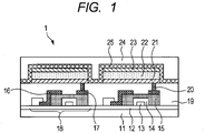
- FIG. 1 is a schematic sectional view of a display apparatus including an organic light-emitting device and a switching device connected to the organic light-emitting device.
- the organic light-emitting device of the present invention includes: an anode; a cathode; an emission layer placed between the anode and the cathode; and an organic compound layer placed between the anode and the emission layer.
- the organic compound layer contains the following compound A and compound B:
- specific constructions of the organic light-emitting device include at least the following constructions (A) to (C).
- the cathode constituting the organic light-emitting device is formed on the substrate as an electrode close to the substrate before the respective layers are formed.
- the organic compound layer incorporated into the organic light-emitting device as a layer different from the emission layer is a layer formed between the anode and the emission layer as described above.
- the layer construction of the organic compound layer is not limited to a single layer and may be a laminate formed of multiple layers.
- the organic compound layer in the organic light-emitting device is preferably a layer having a function of transporting a hole, and is specifically a hole injection layer, a hole transport layer, or a laminate obtained by laminating a hole injection layer and a hole transport layer.
- the SP 3 carbon atoms in the compound A are carbon atoms for forming a saturated carbon-carbon bond (C-C) and are carbon atoms constituting mainly an alkyl group bonded to the main skeleton of the aromatic hydrocarbon compound.
- the compound A is a compound represented by the following general formula [1] or [2].
- Z 1 represents an oxygen atom or a phenyl group that may have a fluorine atom or an alkyl group.
- Ar 1 represents an aliphatic condensed polycyclic group or an aryl group selected from the group consisting of a phenyl group, a fluorenyl group, a biphenyl group, or a naphthyl group, wherein the aliphatic condensed polycyclic group and the aryl group may further have an alkyl group, an alkoxy group, or a halogen atom.
- Ar 1 preferably represents a phenyl group having an alkyl group, a fluorenyl group having an alkyl group, a biphenyl group having an alkyl group, or a naphthyl group having an alkyl group.
- n represents an integer of 1 to 6, provided that when Z 1 represents an oxygen atom, n represents 1 or 2.
- Z 1 represents an oxygen atom
- n represents 1 or 2.
- structures Ar 1 's in parentheses may be identical to or different from each other.
- Ar 2 and Ar 3 each represent an aliphatic condensed polycyclic group or an aryl group selected from the group consisting of a phenyl group, a fluorenyl group, a biphenyl group, or a naphthyl group, wherein the aliphatic condensed polycyclic group and the aryl group may further have an alkyl group, an alkoxy group, or a halogen atom.
- the substituent represented by Ar 2 or Ar 3 in the general formula [2] is preferably a phenyl group having an alkyl group, a fluorenyl group having an alkyl group, a biphenyl group having an alkyl group, or a naphthyl group having an alkyl group.
- Examples of the aliphatic condensed polycyclic group represented by Z 1 include ring structures listed below. It should be noted that the substituent (aryl group or aliphatic condensed polycyclic group) represented by Ar 1, Ar 2 ,or Ar 3 may further have: an alkyl group such as a methyl group, an ethyl group, an n-propyl group, an isopropyl group, an n-butyl group, a tert-butyl group, a sec-butyl group, an octyl group, a 1-adamantyl group, a 2-adamantyl group, a cyclohexyl group, a cyclopentyl group, or a cyclohexylmethyl group; an alkoxy group such as a methoxy group, an ethoxy group, an isopropoxy group, an n-propoxy group, a sec-butoxy group, a tert-butoxy group, or an oc
- the alkyl group is preferably an alkyl group having 10 or less carbon atoms such as an isopropyl group, an n-propyl group, an n-butyl group, a sec-butyl group, a tert-butyl group, an isoamyl group, an adamantyl group, a cyclohexyl group, a cyclopentyl group, or a cyclohexylmethyl group.
- any such substituent promotes the lengthening of the lifetime of the organic light-emitting device because the substituent has good heat stability, plays a considerable role in preventing molecular association in a film, and suppresses the crystallization of the film.
- a branched alkyl group such as an isopropyl group, a tert-butyl group, an isoamyl group, an adamantyl group, a cyclohexyl group, a cyclopentyl group, or a cyclohexylmethyl group is more preferred.
- the presence of any such substituent improves the heat stability of the compound itself.
- the aryl group when the aryl group further has an alkoxy group, the aryl group is preferably substituted with an alkoxy group having 10 or less carbon atoms such as an isopropoxy group, an n-propoxy group, a sec-butoxy group, or a tert-butoxy group as the alkoxy group, and an alkoxy group having a branched alkyl group such as an isopropoxy group, a sec-butoxy group, or a tert-butoxy group is more preferred.
- the aryl group further has a halogen atom
- the halogen atom is preferably fluorine.
- the tertiary amine structure of the compound B refers to a structure formed of a nitrogen atom and three kinds of substituents except hydrogen bonded to the nitrogen atom.
- the compound B is a compound containing one or more tertiary amine structures of this type.
- the compound may be a low-molecular weight compound or may be a high-molecular weight compound.
- the compound having a tertiary amine structure serving as the compound B is, for example, a low-molecular weight compound, the compound is any one of the compounds listed in the following general formulae [11] to [17].
- Ar 21 to Ar 27 , Ar 30 to Ar 35 , Ar 38 to Ar 42 , Ar 46 to Ar 51, Ar 55 to Ar 60 , and Ar 61 to Ar 64 each represent a substituted or unsubstituted, monovalent aryl group, a substituted or unsubstituted, monovalent heterocyclic group, or a substituted or unsubstituted, monovalent alkyl group.
- m represents an integer of 1 to 5.
- the compound B is a high-molecular weight compound
- the compound is, for example, a polymer compound having any one of the general formulae [11] to [17] as a repeating unit.
- Examples of the monovalent aryl group include monovalent substituents such as a phenyl group, a naphthyl group, a pentalenyl group, an indenyl group, an azulenyl group, an anthryl group, a pyrenyl group, an indacenyl group, an acenaphthenyl group, a phenanthryl group, a phenalenyl group, a fluoranthenyl group, an acephenanthryl group, an aceanthryl group, a triphenylenyl group, a chrysenyl group, a naphthacenyl group, a perylenyl group, a pantacenyl group, a biphenyl group, a terphenyl group, and a fluorenyl group.
- monovalent substituents such as a phenyl group, a naphthyl group, a pentalenyl
- Examples of the monovalent heterocyclic group include monovalent substituents such as a thienyl group, a pyrrolyl group, a pyridyl group, an oxazolyl group, an oxadiazolyl group, a thiazolyl group, a thiadiazolyl group, a terthienyl group, a dibenzothiophenyl group, a dibenzofuryl group, and a phenanthryl group.
- monovalent substituents such as a thienyl group, a pyrrolyl group, a pyridyl group, an oxazolyl group, an oxadiazolyl group, a thiazolyl group, a thiadiazolyl group, a terthienyl group, a dibenzothiophenyl group, a dibenzofuryl group, and a phenanthryl group.
- Examples of the monovalent alkyl group include monovalent alkyl groups such as a methyl group, an ethyl group, an n-propyl group, an isopropyl group, an n-butyl group, a tert-butyl group, a sec-butyl group, an octyl group, a 1-adamantyl group, and a 2-adamantyl group.
- an alkyl group having 4 or less carbon atoms such as a methyl group, an ethyl group, an n-propyl group, an isopropyl group, an n-butyl group, a tert-butyl group, or a sec-butyl group is preferred.
- the monovalent aryl group, the monovalent heterocyclic group, or the monovalent alkyl group may have, there are given, for example: an alkyl group such as a methyl group, an ethyl group, an n-propyl group, an isopropyl group, an n-butyl group, a tert-butyl group, a sec-butyl group, an octyl group, a 1-adamantyl group, or a 2-adamantyl group; an aryl group such as a phenyl group, a naphthyl group, a pentalenyl group, an indenyl group, an azulenyl group, an anthryl group, a pyrenyl group, an indacenyl group, an acenaphthenyl group, a phenanthryl group, a phenalenyl group, a fluoranthenyl group, an alkyl group such as
- Ar 28 , Ar 29 , Ar 36 , Ar 37 , Ar 43 to Ar 45 , Ar 52 to Ar 54 , and Ar 65 to Ar 68 each represent a substituted or unsubstituted, divalent aryl group, a substituted or unsubstituted, divalent heterocyclic group, or a substituted or unsubstituted, divalent alkyl group.
- divalent aryl group examples include divalent substituents derived from a phenyl group, a naphthyl group, a pentalenyl group, an indenyl group, an azulenyl group, an anthryl group, a pyrenyl group, an indacenyl group, an acenaphthenyl group, a phenanthryl group, a phenalenyl group, a fluoranthenyl group, an acephenanthryl group, an aceanthryl group, a triphenylenyl group, a chrysenyl group, a naphthacenyl group, a perylenyl group, a pantacenyl group, a biphenyl group, a terphenyl group, and a fluorenyl group.
- divalent heterocyclic group examples include divalent substituents derived from a thienyl group, a pyrrolyl group, a pyridyl group, an oxazolyl group, an oxadiazolyl group, a thiazolyl group, a thiadiazolyl group, a terthienyl group, a dibenzothiophenyl group, a dibenzofuryl group, and a phenanthryl group.
- divalent alkyl group examples include divalent alkyl groups derived from a methyl group, an ethyl group, an n-propyl group, an isopropyl group, an n-butyl group, a tert-butyl group, a sec-butyl group, an octyl group, a 1-adamantyl group, and a 2-adamantyl group.
- a divalent substituent derived from an alkyl group having 4 or less carbon atoms such as a methyl group, an ethyl group, an n-propyl group, an isopropyl group, an n-butyl group, a tert-butyl group, or a sec-butyl group is preferred.
- the aryl group, the heterocyclic group, or the alkyl group may have, there are given, for example: an alkyl group such as a methyl group, an ethyl group, an n-propyl group, an isopropyl group, an n-butyl group, a tert-butyl group, a sec-butyl group, an octyl group, a 1-adamantyl group, or a 2-adamantyl group; an aryl group such as a phenyl group, a naphthyl group, a pentalenyl group, an indenyl group, an azulenyl group, an anthryl group, a pyrenyl group, an indacenyl group, an acenaphthenyl group, a phenanthryl group, a phenalenyl group, a fluoranthenyl group, an acephenanthryl group
- Ar 21 to Ar 23 may be identical to or different from one another.
- any one of the combinations of Ar 21 and Ar 22 , Ar 21 and Ar 23 , and Ar 22 and Ar 23 may wind in a ring (that is, for example, Ar 21 and Ar 22 may be bonded to turn into -Ar 21 -Ar 22 -, thereby forming a ring with N) to form a nitrogen-containing heterocyclic skeleton such as a carbazole skeleton.
- Ar 24 to Ar 27 may be identical to or different from one another.
- any one of the combinations of Ar 24 and Ar 25 , and Ar 26 and Ar 27 may wind in a ring to form a nitrogen-containing heterocyclic skeleton such as a carbazole skeleton.
- Ar 30 to Ar 35 may be identical to or different from one another.
- any one of the combinations of Ar 30 and Ar 31 , Ar 32 and Ar 33 , and Ar 34 and Ar 35 may wind in a ring to form a nitrogen-containing heterocyclic skeleton such as a carbazole skeleton.
- Ar 36 and Ar 37 may be identical to or different from each other.
- Ar 38 to Ar 42 may be identical to or different from one another.
- any one of the combinations of Ar 38 and Ar 39 , and Ar 40 and Ar 41 may wind in a ring to form a nitrogen-containing heterocyclic skeleton such as a carbazole skeleton.
- Ar 43 to Ar 45 may be identical to or different from one another.
- Ar 46 to Ar 51 may be identical to or different from one another.
- any one of the combinations of Ar 46 and Ar 47 , and Ar 49 and Ar 50 may wind in a ring to form a nitrogen-containing heterocyclic skeleton such as a carbazole skeleton.
- Ar 52 to Ar 54 may be identical to or different from one another.
- Ar 55 to Ar 60 may be identical to or different from one another.
- any one of the combinations of Ar 55 and Ar 56 , Ar 57 and Ar 58 , and Ar 59 and Ar 60 may wind in a ring to form a nitrogen-containing heterocyclic skeleton such as a carbazole skeleton.
- Ar 61 to Ar 63 may be identical to or different from one another.
- Ar 65 to Ar 68 may be identical to or different from one another.
- a compound according to the general formula [17] comprehends a polymer compound having a large number (m value) of repeating units.
- the organic light-emitting device of the present invention includes at least one organic compound layer (such as a hole transport layer or an electron-blocking layer) between the anode and the emission layer.
- the organic compound layer contains the compound A and the compound B.
- the organic light-emitting device of the present invention has good emission efficiency.
- the inventors of the present invention have produced an organic light-emitting device having a device construction shown in Table 1 below by using compounds shown below with a view to investigating the operation and effect of the incorporation of the compound A and the compound B into the organic compound layer formed between the anode and the emission layer. It should be noted that multiple compounds different from each other in SP 3 carbon atom content were prepared as compounds each serving as the compound A. Details about the foregoing are described below.
- the produced organic light-emitting device was evaluated for its emission efficiency, external quantum yield, and chromaticity coordinates when caused to emit light under the condition of 2,000 cd/m 2 .
- the relative ratio (%) of the SP 3 carbon atoms in the compound A can be determined from the following equation. It should be noted that the resultant value is rounded off to the nearest integer. [Number of SP 3 carbon atoms in compound A]/[number of SP 2 carbon atoms in compound A] ⁇ 100
- Table 2 shows the results of the evaluations of the emission efficiency, the external quantum yield, and the chromaticity coordinates.
- Table 2 Compound used as compound A SP 3 carbon atom [relative ratio, %] Emission efficiency [cd/A] External quantum yield [%] Chromaticity coordinates [x, y] AC-6 109 13.0 7.0 (0.15, 0.26) AA-1 92 11.7 6.5 (0.16, 0.26) AA-7 87 11.3 6.3 (0.16, 0.26) AA-9 65 11.1 6.2 (0.16, 0.26) AB-3 53 12.3 6.9 (0.16, 0.25) AB-7 44 11.5 6.6 (0.15, 0.25) AB-6 42 12.1 6.8 (0.15, 0.25) AZ-1 25 8.8 4.9 (0.16, 0.24) AZ-2 0 - [Note 1] AZ-3 0 7.8 4.3 (0.15, 0.25) (None) - 8.3 4.7 (0.15, 0.25) [Note 1] AZ-2
- the emission efficiency is improved by incorporating, into the organic compound layer formed between the anode and the emission layer, a compound having a relative ratio (%) of the SP 3 carbon atoms of 40% or more out of the organic compounds each used as the compound A together with the compound B as a hole transportable compound.
- SP 3 carbon atoms generally have the following features (1a-1) and (1a-2):
- SP 2 carbon atoms generally have the following features (1b-1) and (1b-2):
- the feature (1b-2) is a feature caused by the fact that a stacking interaction is strengthened by the presence of a large amount of electrons delocalized by n-electron systems on a rigid planar structure and SP 2 hybrid orbital.
- the feature (1b-2) becomes more significant as the number of n-electrons increases.
- the emission efficiency improves as an SP 3 carbon atom in an alkyl group or the like of an organic compound corresponding to the compound A is incorporated in a certain amount or more, in other words, the ratio of a substituent (such as an alkyl group) formed of an SP 3 carbon atom in a molecule increases.
- the improving effect on the emission efficiency appears when the relative ratio (%) of the SP 3 carbon atoms is 40% or more.
- the relative ratio (%) of the number of the SP 3 carbon atoms in the compound A to the number of the SP 2 carbon atoms in the compound A is 80% or more.
- the structure and substituent of the compound A are not particularly limited as long as the compound has a relative ratio (%) of the SP 3 carbon atoms of 80% or more.
- the compound is preferably of a structure free of a nitrogen atom and a metal atom because the difficulty with which the compound interacts with the compound B is preferably high.
- Ar 1 in the general formula [1], and Ar 2 and Ar 3 in the general formula [2] are each more preferably of a structure having a wide band gap.
- the structure contains a phenyl group, a fluorenyl group, a biphenyl group, or a naphthyl group. This is because the structure has suppressing effects on the movement of an exciton and the injection of an electron.
- a mixing ratio between the compound A and compound B in the organic compound layer is not particularly limited.
- a higher ratio of the compound A may improve the emission efficiency and a higher ratio of the compound B may reduce the driving voltage of the device.
- the ratio (mixing ratio, weight base) of the compound B in the organic compound layer is preferably 10wt% to 90wt%, more preferably 20wt% to 70wt% with reference to the total of the compound A and the compound B.
- an assist material that may promote carrier injection may be incorporated into the organic compound layer in addition to the compound A and the compound B.
- Exemplified Compounds AA-1 to AA-26 are each a compound having the following feature: the compound has a wide band gap and a high glass transition temperature.
- Exemplified Compounds AB-1 to AB-10 are a group of compounds in each of which Ar 1 represents, or Ar 2 and Ar 3 each represent, a biphenyl group.
- Ar 1 represents, or Ar 2 and Ar 3 each represent, a biphenyl group.
- Each compound belonging to the compound group has a wide band gap and a low sublimation temperature because the compound has a rotation axis in a biphenyl skeleton.
- Exemplified Compounds AC-1 to AC-17 are a group of compounds in each of which Ar 1 represents, or Ar 2 and Ar 3 each represent, a phenyl group.
- Ar 1 represents, or Ar 2 and Ar 3 each represent, a phenyl group.
- a compound having a wide band gap is easily designed because the band gap of a phenyl group is wide.
- the sublimation temperature of the compound can be reduced because its molecular weight can be reduced.
- Exemplified Compound AD-2 is a compound in which Ar 1 represents, or Ar 2 and Ar 3 each represent, a naphthyl group.
- the compound has the following feature: the compound has a wide band gap and a high glass transition temperature.
- the organic light-emitting device of the present invention in particular, the compound A (organic compound free of a nitrogen atom and a metal atom) and the compound B (compound having a tertiary amine structure) as main constituent materials have been described above.
- the constituent materials for the organic light-emitting device of the present invention are not limited to the compound A and the compound B. It should be noted that any other constituent material to be incorporated into the organic light-emitting device of the present invention is separately described.
- organic compound A of the present invention and organic compounds (Compounds C-1 to C-3) according to Patent Literatures 3 and 4 listed below are compared from the viewpoint of the first peak value of an absorption spectrum in a dilute solution.
- Compounds C-1 to C-3 above each have a fluoranthene skeleton or a benzofluoranthene skeleton in itself.
- fluoranthene and benzofluoranthene have narrow band gaps, and hence the first peak value of the absorption spectrum of each of the compounds in a dilute solution is 400 nm or more.
- the first peak value of Compound C-1 is 405 nm.
- the first peak value of the phosphorescence emission spectrum of fluorene, which is the mother skeleton of the organic compound of the present invention, in a low-temperature dilute solution is 429 nm.
- Table 4 shows an absorption first peak wavelength (first peak at longer wavelengths) in an absorption spectrum in a toluene dilute solution and a phosphorescence emission peak wavelength at 77 K in a toluene dilute solution.
- Table 4 Compound Absorption first peak wavelength (nm) T 1 (nm) Exemplified Compound AA-1 308 444 Exemplified Compound AA-20 303 443 Compound c-1 405 557 Compound c-11 336 435 Compound c-12 352 462 Compound c-13 303 429 Compound c-21 362 540 Compound c-22 405 566 (Note 1)
- the absorption first peak wavelength is defined from the peak wavelength of the toluene solution (1 ⁇ 10 -6 mol/l) at the longest wavelength.
- a spectrophotometer U-3010 manufactured by Hitachi, Ltd. is used in the measurement. (Note 2) The toluene solution (1 ⁇ 10 -4 mol/l) is cooled to 77 K, its phosphorescence emission component is measured at an excitation wavelength of 320 nm, and the peak wavelength at the shortest wavelength is defined as the T 1 . It should be noted that a spectrophotometer U-3010 manufactured by Hitachi, Ltd. is used in the measurement.
- organic light-emitting device of the present invention materials except the compound A (including a compound corresponding to the organic compound of the present invention) and the compound B
- conventionally known low-molecular weight and high-molecular weight materials can be used as required. More specifically, a hole injectable/transportable material, an emission assist material, an electron injectable/transportable material, or the like can be used.
- the hole injectable/transportable material examples include a triarylamine derivative, a phenylenediamine derivative, a stilbene derivative, a phthalocyanine derivative, a porphyrin derivative, poly(vinyl carbazole), poly(thiophene), and any other conductive polymer. It should be noted that the present invention is not limited to these materials.
- a fluorescent light-emitting material that emits blue, green, or red light such as a triarylamine derivative, a phenylene derivative, a condensed ring aromatic compound (e.g., a fluoranthene derivative, a benzofluoranthene derivative, a pyrene derivative, a chrysene derivative, or a derivative obtained by substitution thereof with a diarylamine), or a stilbene derivative; and a phosphorescent light-emitting material that emits blue, green, or red light such as an organic metal complex (e.g., an organic iridium complex, an organic platinum complex, or a rare earth metal complex).
- an organic metal complex e.g., an organic iridium complex, an organic platinum complex, or a rare earth metal complex
- the content of the guest is preferably 0.1 mass% or more and 30 mass% or less, more preferably 0.5 mass% or more and 10 mass% or less with reference to the total amount of the emission layer.
- the host in the emission layer is a material having the highest weight ratio in the emission layer.
- the host include, but of course not limited to, a triarylamine derivative, a phenylene derivative, a condensed ring aromatic compound (e.g., a naphthalene derivative, a phenanthrene derivative, a fluorene derivative, or a chrysene derivative), an organic metal complex (e.g., an organic aluminum complex such as tris(8-quinolinolato)aluminum, an organic beryllium complex, an organic iridium complex, or an organic platinum complex), and a polymer derivative such as a poly(phenylene vinylene) derivative, a poly(fluorene) derivative, a poly(phenylene) derivative, a poly(thienylene vinylene) derivative, or a poly(acetylene) derivative.
- More specific examples of the host include the group of compounds represented in Table 5.
- Table 5 H1 H2 H3 H4 H5 H6 H7 H8 H9 H10 H1 1 H12 H13 H14 H15 H16 H17 H18 H19 H20 H21 H22 H23 H24
- Examples of the host include, but of course not limited to: condensed ring compounds (such as a fluorene derivative, a naphthalene derivative, an anthracene derivative, a pyrene derivative, a carbazole derivative, a quinoxaline derivative, and a quinoline derivative); an organic aluminum complex such as tris(8-quinolinolato)aluminum; an organic zinc complex; a triphenylamine derivative; and polymer derivatives such as a poly(fluorene) derivative and a poly(phenylene) derivative in addition to the group of compounds represented in Table 5 above.
- condensed ring compounds such as a fluorene derivative, a naphthalene derivative, an anthracene derivative, a pyrene derivative, a carbazole derivative, a quinoxaline derivative, and a quinoline derivative
- an organic aluminum complex such as tris(8-quinolinolato)aluminum
- an organic zinc complex such as
- the electron injectable/transportable material can be arbitrarily selected from materials that allow electrons to be easily injected from the cathode and can transport the injected electrons to the emission layer in consideration of, for example, the balance with the hole mobility of the hole transportable material.
- Examples of the material having electroninjecting performance and electron-transporting performance include an oxadiazole derivative, an oxazole derivative, a pyrazine derivative, a triazole derivative, a triazine derivative, a quinoline derivative, a quinoxaline derivative, a phenanthroline derivative, and an organic aluminum complex.
- a constituent material for the anode desirably has as large a work function as possible.
- Examples thereof may include: metal simple substances such as gold, platinum, silver, copper, nickel, palladium, cobalt, selenium, vanadium, and tungsten or alloys obtained by combining these metal simple substances; metal oxides such as tin oxide, zinc oxide, indium oxide, indium tin oxide (ITO), and indium zinc oxide; and conductive polymers such as polyaniline, polypyrrole, and polythiophene.
- the anode may be of a single-layer construction or may be of a multilayer construction.
- a constituent material for the cathode desirably has as small a work function as possible.
- examples thereof include: metal simple substances such as alkali metals such as lithium; alkaline earth metals such as calcium; and aluminum, titanium, manganese, silver, lead, and chromium.
- alloys obtained by combining those metal simple substances can be used.
- a magnesium-silver alloy, an aluminum-lithium alloy, or an aluminum-magnesium alloy can be used.
- a metal oxide such as indium tin oxide (ITO) can also be utilized.
- ITO indium tin oxide
- the cathode may be of a single-layer construction or may be of a multilayer construction.
- the organic compound layer (such as the hole injection layer, the hole transport layer, the electron-blocking layer, the emission layer, the hole-blocking layer, the electron transport layer, or the electron injection layer) for forming the organic light-emitting device of the present invention is formed by the following method.
- a dry process such as a vacuum deposition method, an ionized vapor deposition method, sputtering, or a plasma process can be used for the formation of the organic compound layer for forming the organic light-emitting device of the present invention.
- a wet process involving dissolving the constituent materials in an appropriate solvent and forming a layer by a known application method (such as spin coating, dipping, a casting method, an LB method, or an ink jet method) can be used instead of the dry process.
- the layer when the layer is formed by the vacuum deposition method, the solution application method, or the like, the layer hardly undergoes crystallization or the like and is excellent in stability over time.
- the film when the layer is formed by the application method, the film can be formed in combination with an appropriate binder resin.
- binder resin examples include, but not limited to, a polyvinyl carbazole resin, a polycarbonate resin, a polyester resin, an ABS resin, an acrylic resin, a polyimide resin, a phenol resin, an epoxy resin, a silicone resin, and a urea resin.
- binder resins may be used alone as a homopolymer or a copolymer, or two or more kinds thereof may be used as a mixture.
- a known additive such as a plasticizer, an antioxidant, or a UV absorber may be used in combination as required.
- the organic light-emitting device of the present invention can be used as a constituent member for a display apparatus or lighting apparatus.
- the organic light-emitting device finds use in applications such as an exposure light source for an image-forming apparatus of an electrophotographic system, a backlight for a liquid crystal display apparatus, and a light-emitting apparatus including a white light source and a color filter.
- the color filter include filters that transmit light beams having three colors, i.e., red, green, and blue colors.
- a display apparatus of the present invention includes the organic light-emitting device of the present invention in its display portion. It should be noted that the display portion includes multiple pixels.
- the pixels each include the organic light-emitting device of the present invention and a transistor as an example of an active device (switching device) or amplifying device for controlling emission luminance, and the anode or cathode of the organic light-emitting device and the drain electrode or source electrode of the transistor are electrically connected to each other.
- the display apparatus can be used as an image display apparatus for a PC or the like.
- the transistor is, for example, a TFT device and the TFT device is provided on, for example, the insulating surface of a substrate.
- the TFT device preferably includes an electrode formed of a transparent oxide semiconductor.
- the display apparatus may be an image information processing apparatus that includes an image input portion for inputting image information from, for example, an area CCD, a linear CCD, or a memory card, and displays an input image on its display portion.
- an image information processing apparatus that includes an image input portion for inputting image information from, for example, an area CCD, a linear CCD, or a memory card, and displays an input image on its display portion.
- the display portion of an imaging apparatus or inkjet printer may have a touch panel function.
- the drive system of the touch panel function is not particularly limited.
- the display apparatus may be used in the display portion of a multifunction printer.
- a lighting apparatus is an apparatus for lighting, for example, the inside of a room.
- the lighting apparatus may emit light having any one of the following colors: a white color (having a color temperature of 4,200 K), a daylight color (having a color temperature of 5,000 K), and colors ranging from blue to red colors.
- a lighting apparatus of the present invention includes the organic light-emitting device of the present invention and an AC/DC converter circuit (circuit for converting an AC voltage into a DC voltage) connected to the organic light-emitting device and supplying a driving voltage to the organic light-emitting device. It should be noted that the lighting apparatus may further include a color filter.
- An image-forming apparatus of the present invention is an image-forming apparatus including: a photosensitive member; a charging portion for charging the surface of the photosensitive member; an exposure portion for exposing the photosensitive member to form an electrostatic latent image; and a developing unit for developing the electrostatic latent image formed on the surface of the photosensitive member.
- the exposing unit to be provided in the image-forming apparatus includes the organic light-emitting device of the present invention.
- the organic light-emitting device of the present invention can be used as a constituent member (light-emitting member) for an exposing machine for exposing a photosensitive member.
- An exposing machine including the organic light-emitting device of the present invention is, for example, an exposing machine in which a plurality of the organic light-emitting devices of the present invention are placed to form a line along a predetermined linear direction.
- FIG. 1 is a schematic sectional view illustrating an example of a display apparatus including an organic light-emitting device and a switching device connected to the organic light-emitting device. It should be noted that the organic light-emitting device of the present invention is used as the organic light-emitting device constituting a display apparatus 1 of FIG. 1 .
- the display apparatus 1 of FIG. 1 includes a substrate 11 made of glass or the like and a moisture-proof film 12 for protecting a TFT device 18 or organic compound layer as the switching device, the film being formed on the substrate.
- a metal gate electrode 13 is represented by reference numeral 13
- a gate insulating film 14 is represented by reference numeral 14
- a semiconductor layer is represented by reference numeral 15.
- the TFT device 18 includes the semiconductor layer 15, a drain electrode 16, and a source electrode 17.
- An insulating film 19 is formed on the TFT device 18.
- An anode 21 constituting the organic light-emitting device and the source electrode 17 are connected to each other through a contact hole 20.
- a system for the electrical connection between the electrode (anode or cathode) in the organic light-emitting device and the electrode (source electrode or drain electrode) in the TFT is not limited to the aspect illustrated in FIG. 1 .
- one of the anode and the cathode, and one of the source electrode and drain electrode of the TFT device have only to be electrically connected to each other.
- an organic compound layer 22 may be multiple layers.
- a first protective layer 24 and second protective layer 25 for suppressing the deterioration of the organic light-emitting device are formed on a cathode 23.
- an emission layer in the organic compound layer 22 in FIG. 1 may be a layer obtained by mixing a red light-emitting material, a green light-emitting material, and a blue light-emitting material.
- the layer may be a laminated emission layer obtained by laminating a layer formed of the red light-emitting material, a layer formed of the green light-emitting material, and a layer formed of the blue light-emitting material.
- the layer formed of the red light-emitting material, the layer formed of the green light-emitting material, and the layer formed of the blue light-emitting material are, for example, arranged side by side to form domains in one emission layer.
- an MIM device may be used instead of the transistor as the switching device.
- the transistor to be used in the display apparatus 1 of FIG. 1 is not limited to a transistor using a monocrystalline silicon wafer and may be a thin-film transistor including an active layer on the insulating surface of a substrate.
- a thin-film transistor using monocrystalline silicon as the active layer, a thin-film transistor using non-monocrystalline silicon such as amorphous silicon or microcrystalline silicon as the active layer, or a thin-film transistor using a non-monocrystalline oxide semiconductor such as an indium zinc oxide or an indium gallium zinc oxide as the active layer is also permitted.
- the thin-film transistor is also called a TFT device.
- the transistor in the display apparatus 1 of FIG. 1 may be formed in a substrate such as an Si substrate.
- a substrate such as an Si substrate.
- the phrase "formed in a substrate” means that the transistor is produced by processing the substrate itself such as an Si substrate.
- the presence of the transistor in the substrate can be regarded as follows: the substrate and the transistor are integrally formed.
- the transistor is provided in the substrate is selected depending on definition. In the case of, for example, a definition of about a QVGA per inch, the organic light-emitting device is preferably provided in the Si substrate.
- the driving of the display apparatus using the organic light-emitting device of the present invention enables display that has good image quality and is stable over a long time period.
- Mass spectrometry confirmed 611 as the M + of Exemplified Compound AA-1.
- 1 H-NMR measurement confirmed the structure of Exemplified Compound AA-1.
- Exemplified Compound AA-6 was synthesized according to the following synthesis scheme.
- Exemplified Compound AA-8 was synthesized according to the following synthesis scheme.
- Mass spectrometry confirmed 991 as the M + of Exemplified Compound AA-8.
- Exemplified Compound AA-9 was synthesized according to the following synthesis scheme.
- Mass spectrometry confirmed 737 as the M + of Exemplified Compound AA-9.
- 1 H-NMR measurement confirmed the structure of Exemplified Compound AA-9.
- Mass spectrometry confirmed 627 as the M + of Exemplified Compound AA-20.
- 1 H-NMR measurement confirmed the structure of Exemplified Compound AA-20.
- Exemplified Compound AA-2 was synthesized by the same method as that of Example 1 except that: Compound b-10 was synthesized by using Compound b-9 instead of Compound b-1 in the section (1) of Example 1; and Compound b-9 was used instead of Compound b-1 and Compound b-10 was used instead of Compound b-3 in the section (2) of Example 1.
- Mass spectrometry confirmed 923 as the M + of Exemplified Compound AA-2.
- Exemplified Compound AA-13 was synthesized by the same method as that of Example 1 except that Compound b-11 (1,4-dibromonaphthalene) was used instead of Compound b-1 in the section (2) of Example 1.
- Mass spectrometry confirmed 763 as the M + of Exemplified Compound AA-13.
- Exemplified Compound AA-28 was synthesized by the same method as that of Example 1 except that Compound b-12 was used instead of Compound b-1 in the section (2) of Example 1.
- Mass spectrometry confirmed 538 as the M + of Exemplified Compound AA-28.
- Exemplified Compound AA-35 was synthesized by the same method as that of Example 1 except that Compound b-13 (1,3,5-tribromobenzene) was used instead of Compound b-1 in the section (2) of Example 1.
- Mass spectrometry confirmed 1,141 as the M + of Exemplified Compound AA-35.
- Comparative Compound AZ-1 was synthesized by the same method as that of Example 4 except that Compound b-32 was used instead of 1,4-dibromonaphthalene and Compound b-31 was used instead of Compound b-3 in Example 4. Mass spectrometry confirmed 578 as the M + of Comparative Compound AZ-1.
- Exemplified Compound AB-3 was synthesized according to the following synthesis scheme.
- Mass spectrometry confirmed 607 as the M + of Exemplified Compound AB-3.
- Exemplified Compound AC-6 was synthesized according to the following synthesis scheme.
- Mass spectrometry confirmed 617 as the M + of Exemplified Compound AC-6.
- 1 H-NMR measurement confirmed the structure of Exemplified Compound AC-6.
- Exemplified Compound AB-7 was synthesized by the same method as that of Synthesis Example 1 except that Compound b-14 was used instead of 1,3-dibromobenzene in Synthesis Example 1.
- Mass spectrometry confirmed 683 as the M + of Exemplified Compound AB-7.
- Exemplified Compound AB-6 was synthesized according to the following synthesis scheme.
- Mass spectrometry confirmed 707 as the M + of Exemplified Compound AB-6.
- an organic light-emitting device in which an anode, a hole transport layer, an emission layer, a hole-blocking layer, an electron transport layer, and a cathode were formed in the stated order on a substrate was produced by a method described below.
- part of the compounds used in this example are listed below.
- ITO Indium tin oxide
- IPA isopropyl alcohol
- the dried product was subjected to UV/ozone washing, and the resultant was used as a transparent conductive supporting substrate in the following steps.
- Exemplified Compound AC-6 (hereinafter referred to as “compound A”) and chloroform were mixed to prepare a material solution A having a concentration of 0.25 wt%.
- compound A Exemplified Compound AC-6
- compound B Compound B
- chloroform was mixed to prepare a material solution B having a concentration of 0.25 wt%.
- a mixed liquid was prepared by mixing the material solution A and the material solution B so that their weight ratio became 2:1.
- the mixed liquid was dropped onto the anode (ITO electrode) and then a thin film was formed by spin coating at 500 RPM for 10 seconds and then at 1,000 RPM for 1 minute. After that, the solvent in the thin film was completely removed by drying the thin film in a vacuum oven at 80°C for 10 minutes. Thus, the hole transport layer was formed. At this time, the thickness of the hole transport layer was 30 nm.
- a current was passed through the resultant organic light-emitting device, and then its emission characteristics when its emission luminance was set to 2,000 cd/m 2 were measured and evaluated.
- the device had an emission efficiency (cd/A) of 13.0 cd/A and an external quantum yield of 7.5%.
- the device had CIE chromaticity coordinates of (0.16, 0.26) and was observed to emit blue light satisfactorily.
- Organic light-emitting devices were each produced by the same method as that of Example 11 except that the compound A and the compound B were changed to compounds shown in Table 7 below in Example 11. In addition, the resultant organic light-emitting devices were evaluated by the same method as that of Example 11. Table 7 shows the results.
- Organic light-emitting devices were each produced by the same method as that of Example 11 except that Exemplified Compound AA-1 was used as the compound A and the compound B was changed to a compound shown in Table 7 below in Example 11. In addition, the resultant organic light-emitting devices were evaluated by the same method as that of Example 11. Table 7 shows the results.
- Organic light-emitting devices were each produced by the same method as that of Example 11 except that the compound A and the compound B were changed to compounds shown in Table 8 below in Example 11. In addition, the resultant organic light-emitting devices were evaluated by the same method as that of Example 11. Table 8 shows the results.
- An organic light-emitting device was produced by the same method as that of Example 11 except that the hole transport layer was formed using only the material solution B in Example 11.
- the resultant organic light-emitting device was evaluated by the same method as that of Example 11. Table 8 shows the results.
- Organic light-emitting devices were each produced by the same method as that of Comparative Example 4 except that the compound B was changed to a compound shown in Table 8 below in Comparative Example 4. In addition, the resultant organic light-emitting devices were evaluated by the same method as that of Example 11. Table 8 shows the results. Table 8 Compound A Compound B Emission efficiency [cd/A] External quantum yield [%] Chromaticity coordinates [x, y] Comparative Example 1 AZ-1 BC-4 8.8 4.9 (0.16, 0.24) Comparative Example 2 AZ-2 BC-4 AZ-2 emitted light.
- Comparative Example 3 AZ-3 BC-4 7.8 4.3 (0.15, 0.25) Comparative Example 4 - BC-4 8.3 4.7 (0.15, 0.25) Comparative Example 5 - BB-4 3.2 1.8 (0.15, 0.25) Comparative Example 6 - BF-1 2.4 1.3 (0.15, 0.25) Comparative Example 7 - BF-2 2.2 1.2 (0.15, 0.25)
- an organic light-emitting device was produced.
- An organic light-emitting device in which an anode, a hole transport layer, an emission layer, a hole-blocking layer, an electron transport layer, and a cathode were formed in the stated order on a substrate was produced by a method described below.
- part of the compounds used in this example are listed below.
- a transparent conductive supporting substrate was produced by the same method as that of Example 11.
- a chloroform solution having a concentration of 0.25 wt% was prepared by mixing Exemplified Compound AA-1 and chloroform.
- the chloroform solution was dropped onto the anode (ITO electrode) and then a thin film was formed by spin coating at 500 RPM for 10 seconds and then at 1,000 RPM for 1 minute. After that, the solvent in the thin film was completely removed by drying the thin film in a vacuum oven at 80°C for 10 minutes. Thus, the hole transport layer was formed. At this time, the thickness of the hole transport layer was 30 nm.
- a current was passed through the resultant organic light-emitting device, and then its emission characteristics when its emission luminance was set to 2,000 cd/m 2 were measured and evaluated.
- the device had an emission efficiency (cd/A) of 7.2 cd/A and was observed to emit blue light satisfactorily.
- An organic light-emitting device was produced by the same method as that of Example 21 except that Exemplified Compound AA-20 was used instead of Exemplified Compound AA-1 in Example 21.
- the emission characteristics of the organic light-emitting device were measured and evaluated by the same method as that of Example 21. As a result, the device had an emission efficiency (cd/A) of 8.0 cd/A and was observed to emit blue light satisfactorily.
- An organic light-emitting device was produced by the same method as that of Example 21 except that Exemplified Compound AA-35 was used instead of Exemplified Compound AA-1 in Example 21.
- the emission characteristics of the organic light-emitting device were measured and evaluated by the same method as that of Example 21. As a result, the device had an emission efficiency (cd/A) of 7.1 cd/A and was observed to emit blue light satisfactorily.
- ITO Indium tin oxide
- IPA isopropyl alcohol
- a predetermined voltage was applied to the resultant organic light-emitting device while its ITO electrode was defined as a positive electrode and its Al electrode was defined as a negative electrode.
- the device was observed to emit blue light having CIE chromaticity coordinates of (0.21, 0.48).
- An organic light-emitting device was produced by the same method as that of Example 24 except that Exemplified Compound AA-20 was used instead of Exemplified Compound AA-1 in Example 24.
- the emission characteristics of the organic light-emitting device were measured and evaluated by the same method as that of Example 24. As a result, the device was observed to emit blue light having CIE chromaticity coordinates of (0.21, 0.48).
- TFT device 20: anode
- 21 organic compound layer
- 22 cathode
Landscapes
- Chemical & Material Sciences (AREA)
- Organic Chemistry (AREA)
- Engineering & Computer Science (AREA)
- Physics & Mathematics (AREA)
- Spectroscopy & Molecular Physics (AREA)
- Materials Engineering (AREA)
- General Physics & Mathematics (AREA)
- Theoretical Computer Science (AREA)
- General Engineering & Computer Science (AREA)
- Human Computer Interaction (AREA)
- Microelectronics & Electronic Packaging (AREA)
- Electroluminescent Light Sources (AREA)
- Organic Low-Molecular-Weight Compounds And Preparation Thereof (AREA)
Priority Applications (1)
| Application Number | Priority Date | Filing Date | Title |
|---|---|---|---|
| EP22171994.1A EP4075533B1 (en) | 2013-04-03 | 2014-04-03 | Organic compound and organic light-emitting device |
Applications Claiming Priority (3)
| Application Number | Priority Date | Filing Date | Title |
|---|---|---|---|
| JP2013077439 | 2013-04-03 | ||
| JP2014076287A JP6444046B2 (ja) | 2013-04-03 | 2014-04-02 | 有機化合物及び有機発光素子 |
| PCT/JP2014/060350 WO2014163211A1 (en) | 2013-04-03 | 2014-04-03 | Organic compound and organic light-emitting device |
Related Child Applications (1)
| Application Number | Title | Priority Date | Filing Date |
|---|---|---|---|
| EP22171994.1A Division EP4075533B1 (en) | 2013-04-03 | 2014-04-03 | Organic compound and organic light-emitting device |
Publications (3)
| Publication Number | Publication Date |
|---|---|
| EP2981993A1 EP2981993A1 (en) | 2016-02-10 |
| EP2981993A4 EP2981993A4 (en) | 2017-04-12 |
| EP2981993B1 true EP2981993B1 (en) | 2022-05-11 |
Family
ID=51658495
Family Applications (2)
| Application Number | Title | Priority Date | Filing Date |
|---|---|---|---|
| EP22171994.1A Active EP4075533B1 (en) | 2013-04-03 | 2014-04-03 | Organic compound and organic light-emitting device |
| EP14778819.4A Active EP2981993B1 (en) | 2013-04-03 | 2014-04-03 | Organic compound and organic light-emitting device |
Family Applications Before (1)
| Application Number | Title | Priority Date | Filing Date |
|---|---|---|---|
| EP22171994.1A Active EP4075533B1 (en) | 2013-04-03 | 2014-04-03 | Organic compound and organic light-emitting device |
Country Status (4)
| Country | Link |
|---|---|
| US (1) | US9911921B2 (enExample) |
| EP (2) | EP4075533B1 (enExample) |
| JP (1) | JP6444046B2 (enExample) |
| WO (1) | WO2014163211A1 (enExample) |
Families Citing this family (5)
| Publication number | Priority date | Publication date | Assignee | Title |
|---|---|---|---|---|
| JP6444046B2 (ja) | 2013-04-03 | 2018-12-26 | キヤノン株式会社 | 有機化合物及び有機発光素子 |
| JP6552201B2 (ja) | 2015-01-19 | 2019-07-31 | キヤノン株式会社 | 有機発光素子 |
| JP2018163975A (ja) * | 2017-03-24 | 2018-10-18 | 出光興産株式会社 | 組成物、有機エレクトロルミネッセンス素子用材料、組成物膜、有機エレクトロルミネッセンス素子、及び電子機器 |
| JP7224796B2 (ja) | 2018-07-03 | 2023-02-20 | キヤノン株式会社 | 白色有機発光素子 |
| KR20240048513A (ko) * | 2021-08-13 | 2024-04-15 | 이데미쓰 고산 가부시키가이샤 | 조성물, 유기 일렉트로루미네센스 소자, 및 전자 기기 |
Citations (1)
| Publication number | Priority date | Publication date | Assignee | Title |
|---|---|---|---|---|
| US5989737A (en) * | 1997-02-27 | 1999-11-23 | Xerox Corporation | Organic electroluminescent devices |
Family Cites Families (48)
| Publication number | Priority date | Publication date | Assignee | Title |
|---|---|---|---|---|
| JP3825725B2 (ja) | 1998-05-19 | 2006-09-27 | 三洋電機株式会社 | 有機エレクトロルミネッセンス素子 |
| JP2000068064A (ja) | 1998-08-26 | 2000-03-03 | Toray Ind Inc | 発光素子 |
| JP3848262B2 (ja) | 2002-03-27 | 2006-11-22 | キヤノン株式会社 | オリゴフルオレニレン化合物及び有機発光素子 |
| JP2003332074A (ja) | 2002-05-09 | 2003-11-21 | Canon Inc | 金属配位化合物を用いた発光素子 |
| JP4164317B2 (ja) | 2002-08-28 | 2008-10-15 | キヤノン株式会社 | 有機発光素子 |
| JP4311707B2 (ja) | 2002-08-28 | 2009-08-12 | キヤノン株式会社 | 有機発光素子 |
| JP4125076B2 (ja) | 2002-08-30 | 2008-07-23 | キヤノン株式会社 | モノアミノフルオレン化合物およびそれを使用した有機発光素子 |
| JP4261948B2 (ja) * | 2003-03-18 | 2009-05-13 | 三井化学株式会社 | フルオレン化合物、および該フルオレン化合物を含有する有機電界発光素子 |
| JP3848307B2 (ja) | 2003-06-27 | 2006-11-22 | キヤノン株式会社 | アミノアントリル誘導基置換化合物およびそれを使用した有機発光素子 |
| JP3840235B2 (ja) | 2003-06-27 | 2006-11-01 | キヤノン株式会社 | 有機発光素子 |
| JP4789475B2 (ja) * | 2004-03-10 | 2011-10-12 | 富士フイルム株式会社 | 発光素子 |
| US7662485B2 (en) * | 2004-03-16 | 2010-02-16 | Eastman Kodak Company | White organic light-emitting devices with improved performance |
| JP2005293992A (ja) * | 2004-03-31 | 2005-10-20 | Sanyo Electric Co Ltd | 有機エレクトロルミネッセンス素子の製造方法 |
| JP4599142B2 (ja) | 2004-11-26 | 2010-12-15 | キヤノン株式会社 | 有機発光素子 |
| JP4429149B2 (ja) | 2004-11-26 | 2010-03-10 | キヤノン株式会社 | フルオレン化合物及び有機発光素子 |
| JP4955971B2 (ja) | 2004-11-26 | 2012-06-20 | キヤノン株式会社 | アミノアントリル誘導基置換ピレン化合物および有機発光素子 |
| US7351999B2 (en) * | 2004-12-16 | 2008-04-01 | Au Optronics Corporation | Organic light-emitting device with improved layer structure |
| US8486487B2 (en) * | 2005-02-17 | 2013-07-16 | Konica Minolta Holdings, Inc. | Gas barrier film, gas barrier film manufacturing method, resin substrate for organic electroluminescent device using the aforesaid gas barrier film, and organic electroluminescent device using the aforementioned gas barrier film |
| JP4659695B2 (ja) | 2005-11-01 | 2011-03-30 | キヤノン株式会社 | フルオレン化合物及び有機発光素子 |
| JP4653061B2 (ja) | 2005-12-20 | 2011-03-16 | キヤノン株式会社 | アミン化合物および有機発光素子および青色有機発光素子 |
| JP5268247B2 (ja) | 2005-12-20 | 2013-08-21 | キヤノン株式会社 | 4−アミノフルオレン化合物及び有機発光素子 |
| JP4871613B2 (ja) | 2006-03-02 | 2012-02-08 | キヤノン株式会社 | 有機発光素子 |
| JP5164389B2 (ja) | 2006-03-28 | 2013-03-21 | キヤノン株式会社 | 有機発光素子用アミノ化合物およびそれを有する有機発光素子 |
| JP4785594B2 (ja) | 2006-03-31 | 2011-10-05 | キヤノン株式会社 | イリジウム錯体の製造方法、有機エレクトロルミネッセンス素子および表示装置 |
| JP4795268B2 (ja) | 2006-04-20 | 2011-10-19 | キヤノン株式会社 | 有機発光素子 |
| JP4818159B2 (ja) | 2006-04-27 | 2011-11-16 | キヤノン株式会社 | フルオランテン誘導体およびそれを有する有機発光素子 |
| JP4819655B2 (ja) | 2006-04-27 | 2011-11-24 | キヤノン株式会社 | 4−アリールフルオレン化合物及びそれを用いた有機発光素子 |
| JP5127206B2 (ja) | 2006-11-28 | 2013-01-23 | キヤノン株式会社 | 金属錯体化合物、有機発光素子及び表示装置 |
| JP2008137978A (ja) | 2006-12-05 | 2008-06-19 | Canon Inc | カルバゾール誘導体及びこれを用いた有機発光素子 |
| JP4939207B2 (ja) | 2006-12-27 | 2012-05-23 | キヤノン株式会社 | カルバゾール化合物及びそれを用いた有機発光素子 |
| JP2008308449A (ja) * | 2007-06-15 | 2008-12-25 | Canon Inc | 縮合環芳香族化合物及びそれを用いた有機発光素子 |
| JP2009040728A (ja) | 2007-08-09 | 2009-02-26 | Canon Inc | 有機金属錯体及びこれを用いた有機発光素子 |
| JP5574563B2 (ja) * | 2007-09-19 | 2014-08-20 | キヤノン株式会社 | フルオレン化合物及びそれを用いた有機電界発光素子並びに表示装置 |
| JP4980938B2 (ja) * | 2008-01-18 | 2012-07-18 | 三井化学株式会社 | 有機電界発光素子 |
| JP5243972B2 (ja) * | 2008-02-28 | 2013-07-24 | ユー・ディー・シー アイルランド リミテッド | 有機電界発光素子 |
| JP5424681B2 (ja) * | 2008-04-01 | 2014-02-26 | キヤノン株式会社 | 有機発光素子 |
| JP5495292B2 (ja) * | 2009-06-23 | 2014-05-21 | Necライティング株式会社 | 照明装置及びダクトレール |
| JP5600895B2 (ja) | 2009-06-26 | 2014-10-08 | 富士ゼロックス株式会社 | 有機電界発光素子、露光装置、プロセスカートリッジ、画像形成装置、表示装置、有機電界発光素子の駆動方法 |
| JP2011151116A (ja) | 2010-01-20 | 2011-08-04 | Canon Inc | 有機発光素子 |
| JP5669539B2 (ja) | 2010-12-01 | 2015-02-12 | キヤノン株式会社 | キノリノ[3,2,1−kl]フェノキサジン化合物及びこれを用いた有機発光素子 |
| JP5669550B2 (ja) | 2010-12-10 | 2015-02-12 | キヤノン株式会社 | インドロフェノキサジン化合物及びこれを用いた有機発光素子 |
| JP5858653B2 (ja) | 2011-06-08 | 2016-02-10 | キヤノン株式会社 | 6,12−ジナフチルクリセン誘導体及びこれを用いた有機発光素子 |
| JP2013077439A (ja) | 2011-09-30 | 2013-04-25 | Sumitomo Chemical Co Ltd | 導光板および面光源装置 |
| JP6228787B2 (ja) | 2012-09-24 | 2017-11-08 | 日本電産サンキョー株式会社 | 便座便蓋開閉用ギヤードモータユニット |
| JP6444046B2 (ja) | 2013-04-03 | 2018-12-26 | キヤノン株式会社 | 有機化合物及び有機発光素子 |
| JP6271853B2 (ja) | 2013-04-03 | 2018-01-31 | キヤノン株式会社 | 有機発光素子、表示装置、画像情報処理装置及び画像形成装置 |
| JP6335530B2 (ja) | 2014-01-29 | 2018-05-30 | キヤノン株式会社 | 有機発光素子 |
| JP6472246B2 (ja) | 2014-03-24 | 2019-02-20 | キヤノン株式会社 | 有機発光素子 |
-
2014
- 2014-04-02 JP JP2014076287A patent/JP6444046B2/ja active Active
- 2014-04-03 EP EP22171994.1A patent/EP4075533B1/en active Active
- 2014-04-03 EP EP14778819.4A patent/EP2981993B1/en active Active
- 2014-04-03 WO PCT/JP2014/060350 patent/WO2014163211A1/en not_active Ceased
- 2014-04-03 US US14/766,298 patent/US9911921B2/en active Active
Patent Citations (1)
| Publication number | Priority date | Publication date | Assignee | Title |
|---|---|---|---|---|
| US5989737A (en) * | 1997-02-27 | 1999-11-23 | Xerox Corporation | Organic electroluminescent devices |
Also Published As
| Publication number | Publication date |
|---|---|
| US9911921B2 (en) | 2018-03-06 |
| JP6444046B2 (ja) | 2018-12-26 |
| JP2014212315A (ja) | 2014-11-13 |
| WO2014163211A1 (en) | 2014-10-09 |
| EP2981993A1 (en) | 2016-02-10 |
| EP4075533A1 (en) | 2022-10-19 |
| EP4075533B1 (en) | 2024-07-03 |
| EP2981993A4 (en) | 2017-04-12 |
| US20150372238A1 (en) | 2015-12-24 |
Similar Documents
| Publication | Publication Date | Title |
|---|---|---|
| EP2939289B1 (en) | Organic light-emitting element | |
| EP3357912B1 (en) | Use of spiro compound and organic light emitting element comprising same | |
| EP3378864B1 (en) | Spiro compound and organic light-emitting element comprising same | |
| US20130175519A1 (en) | New condensed polycyclic compound and organic light-emitting element using the same | |
| CN111356689B (zh) | 化合物及包含其的有机发光器件 | |
| CN104703952B (zh) | 新型有机化合物和具有该有机化合物的有机发光器件和显示装置 | |
| JP4659695B2 (ja) | フルオレン化合物及び有機発光素子 | |
| CN105492413A (zh) | 蒽衍生物和使用该蒽衍生物的有机电致发光元件 | |
| EP3378865B1 (en) | Spiro compound and organic light-emitting element comprising same | |
| EP2981993B1 (en) | Organic compound and organic light-emitting device | |
| JP5479003B2 (ja) | 有機発光素子 | |
| JP6271853B2 (ja) | 有機発光素子、表示装置、画像情報処理装置及び画像形成装置 | |
| KR20240032784A (ko) | 화합물 및 이를 포함하는 유기 발광 소자 | |
| CN104684876A (zh) | 茚并[1, 2-b]菲化合物和包括该化合物的有机发光元件 | |
| US20120132901A1 (en) | Pyrene derivative and organic light-emitting device using the same | |
| EP4212535B1 (en) | Compound and organic light-emitting element comprising same | |
| KR102563303B1 (ko) | 헤테로 고리 화합물, 이를 포함하는 유기 발광 소자, 이의 제조방법 및 유기물층용 조성물 | |
| KR20180008337A (ko) | 헤테로고리 화합물 및 이를 포함하는 유기 발광 소자 | |
| CN116601137B (zh) | 胺系化合物及包含其的有机发光器件 | |
| JP6047116B2 (ja) | 新規なアントラセン化合物及びこれを用いた有機エレクトロルミネッセンス素子 | |
| EP4446316A1 (en) | Compound and organic light-emitting device comprising same | |
| WO2011138907A1 (en) | Novel organic compound | |
| JP2015153993A (ja) | 有機発光素子 | |
| WO2010053141A1 (en) | Dibenzo[c,g]fluorene compound and organic light-emitting device using same |
Legal Events
| Date | Code | Title | Description |
|---|---|---|---|
| PUAI | Public reference made under article 153(3) epc to a published international application that has entered the european phase |
Free format text: ORIGINAL CODE: 0009012 |
|
| 17P | Request for examination filed |
Effective date: 20151103 |
|
| AK | Designated contracting states |
Kind code of ref document: A1 Designated state(s): AL AT BE BG CH CY CZ DE DK EE ES FI FR GB GR HR HU IE IS IT LI LT LU LV MC MK MT NL NO PL PT RO RS SE SI SK SM TR |
|
| AX | Request for extension of the european patent |
Extension state: BA ME |
|
| DAX | Request for extension of the european patent (deleted) | ||
| REG | Reference to a national code |
Ref country code: DE Ref legal event code: R079 Ref document number: 602014083706 Country of ref document: DE Free format text: PREVIOUS MAIN CLASS: H01L0051500000 Ipc: H01L0051540000 |
|
| A4 | Supplementary search report drawn up and despatched |
Effective date: 20170315 |
|
| RIC1 | Information provided on ipc code assigned before grant |
Ipc: H01L 51/54 20060101AFI20170309BHEP Ipc: C07C 13/567 20060101ALI20170309BHEP Ipc: G09F 9/30 20060101ALI20170309BHEP Ipc: C07C 25/22 20060101ALI20170309BHEP Ipc: H01L 27/32 20060101ALI20170309BHEP Ipc: C07C 43/275 20060101ALI20170309BHEP |
|
| STAA | Information on the status of an ep patent application or granted ep patent |
Free format text: STATUS: EXAMINATION IS IN PROGRESS |
|
| 17Q | First examination report despatched |
Effective date: 20190626 |
|
| GRAP | Despatch of communication of intention to grant a patent |
Free format text: ORIGINAL CODE: EPIDOSNIGR1 |
|
| STAA | Information on the status of an ep patent application or granted ep patent |
Free format text: STATUS: GRANT OF PATENT IS INTENDED |
|
| INTG | Intention to grant announced |
Effective date: 20211118 |
|
| GRAS | Grant fee paid |
Free format text: ORIGINAL CODE: EPIDOSNIGR3 |
|
| GRAA | (expected) grant |
Free format text: ORIGINAL CODE: 0009210 |
|
| STAA | Information on the status of an ep patent application or granted ep patent |
Free format text: STATUS: THE PATENT HAS BEEN GRANTED |
|
| AK | Designated contracting states |
Kind code of ref document: B1 Designated state(s): AL AT BE BG CH CY CZ DE DK EE ES FI FR GB GR HR HU IE IS IT LI LT LU LV MC MK MT NL NO PL PT RO RS SE SI SK SM TR |
|
| REG | Reference to a national code |
Ref country code: GB Ref legal event code: FG4D |
|
| REG | Reference to a national code |
Ref country code: CH Ref legal event code: EP |
|
| REG | Reference to a national code |
Ref country code: AT Ref legal event code: REF Ref document number: 1492221 Country of ref document: AT Kind code of ref document: T Effective date: 20220515 |
|
| REG | Reference to a national code |
Ref country code: DE Ref legal event code: R096 Ref document number: 602014083706 Country of ref document: DE |
|
| REG | Reference to a national code |
Ref country code: IE Ref legal event code: FG4D |
|
| REG | Reference to a national code |
Ref country code: LT Ref legal event code: MG9D |
|
| REG | Reference to a national code |
Ref country code: NL Ref legal event code: MP Effective date: 20220511 |
|
| REG | Reference to a national code |
Ref country code: AT Ref legal event code: MK05 Ref document number: 1492221 Country of ref document: AT Kind code of ref document: T Effective date: 20220511 |
|
| PG25 | Lapsed in a contracting state [announced via postgrant information from national office to epo] |
Ref country code: SE Free format text: LAPSE BECAUSE OF FAILURE TO SUBMIT A TRANSLATION OF THE DESCRIPTION OR TO PAY THE FEE WITHIN THE PRESCRIBED TIME-LIMIT Effective date: 20220511 Ref country code: PT Free format text: LAPSE BECAUSE OF FAILURE TO SUBMIT A TRANSLATION OF THE DESCRIPTION OR TO PAY THE FEE WITHIN THE PRESCRIBED TIME-LIMIT Effective date: 20220912 Ref country code: NO Free format text: LAPSE BECAUSE OF FAILURE TO SUBMIT A TRANSLATION OF THE DESCRIPTION OR TO PAY THE FEE WITHIN THE PRESCRIBED TIME-LIMIT Effective date: 20220811 Ref country code: NL Free format text: LAPSE BECAUSE OF FAILURE TO SUBMIT A TRANSLATION OF THE DESCRIPTION OR TO PAY THE FEE WITHIN THE PRESCRIBED TIME-LIMIT Effective date: 20220511 Ref country code: LT Free format text: LAPSE BECAUSE OF FAILURE TO SUBMIT A TRANSLATION OF THE DESCRIPTION OR TO PAY THE FEE WITHIN THE PRESCRIBED TIME-LIMIT Effective date: 20220511 Ref country code: HR Free format text: LAPSE BECAUSE OF FAILURE TO SUBMIT A TRANSLATION OF THE DESCRIPTION OR TO PAY THE FEE WITHIN THE PRESCRIBED TIME-LIMIT Effective date: 20220511 Ref country code: GR Free format text: LAPSE BECAUSE OF FAILURE TO SUBMIT A TRANSLATION OF THE DESCRIPTION OR TO PAY THE FEE WITHIN THE PRESCRIBED TIME-LIMIT Effective date: 20220812 Ref country code: FI Free format text: LAPSE BECAUSE OF FAILURE TO SUBMIT A TRANSLATION OF THE DESCRIPTION OR TO PAY THE FEE WITHIN THE PRESCRIBED TIME-LIMIT Effective date: 20220511 Ref country code: ES Free format text: LAPSE BECAUSE OF FAILURE TO SUBMIT A TRANSLATION OF THE DESCRIPTION OR TO PAY THE FEE WITHIN THE PRESCRIBED TIME-LIMIT Effective date: 20220511 Ref country code: BG Free format text: LAPSE BECAUSE OF FAILURE TO SUBMIT A TRANSLATION OF THE DESCRIPTION OR TO PAY THE FEE WITHIN THE PRESCRIBED TIME-LIMIT Effective date: 20220811 Ref country code: AT Free format text: LAPSE BECAUSE OF FAILURE TO SUBMIT A TRANSLATION OF THE DESCRIPTION OR TO PAY THE FEE WITHIN THE PRESCRIBED TIME-LIMIT Effective date: 20220511 |
|
| REG | Reference to a national code |
Ref country code: DE Ref legal event code: R079 Ref document number: 602014083706 Country of ref document: DE Free format text: PREVIOUS MAIN CLASS: H01L0051540000 Ipc: H10K0085000000 |
|
| PG25 | Lapsed in a contracting state [announced via postgrant information from national office to epo] |
Ref country code: RS Free format text: LAPSE BECAUSE OF FAILURE TO SUBMIT A TRANSLATION OF THE DESCRIPTION OR TO PAY THE FEE WITHIN THE PRESCRIBED TIME-LIMIT Effective date: 20220511 Ref country code: PL Free format text: LAPSE BECAUSE OF FAILURE TO SUBMIT A TRANSLATION OF THE DESCRIPTION OR TO PAY THE FEE WITHIN THE PRESCRIBED TIME-LIMIT Effective date: 20220511 Ref country code: LV Free format text: LAPSE BECAUSE OF FAILURE TO SUBMIT A TRANSLATION OF THE DESCRIPTION OR TO PAY THE FEE WITHIN THE PRESCRIBED TIME-LIMIT Effective date: 20220511 Ref country code: IS Free format text: LAPSE BECAUSE OF FAILURE TO SUBMIT A TRANSLATION OF THE DESCRIPTION OR TO PAY THE FEE WITHIN THE PRESCRIBED TIME-LIMIT Effective date: 20220911 |
|
| PG25 | Lapsed in a contracting state [announced via postgrant information from national office to epo] |
Ref country code: SM Free format text: LAPSE BECAUSE OF FAILURE TO SUBMIT A TRANSLATION OF THE DESCRIPTION OR TO PAY THE FEE WITHIN THE PRESCRIBED TIME-LIMIT Effective date: 20220511 Ref country code: SK Free format text: LAPSE BECAUSE OF FAILURE TO SUBMIT A TRANSLATION OF THE DESCRIPTION OR TO PAY THE FEE WITHIN THE PRESCRIBED TIME-LIMIT Effective date: 20220511 Ref country code: RO Free format text: LAPSE BECAUSE OF FAILURE TO SUBMIT A TRANSLATION OF THE DESCRIPTION OR TO PAY THE FEE WITHIN THE PRESCRIBED TIME-LIMIT Effective date: 20220511 Ref country code: EE Free format text: LAPSE BECAUSE OF FAILURE TO SUBMIT A TRANSLATION OF THE DESCRIPTION OR TO PAY THE FEE WITHIN THE PRESCRIBED TIME-LIMIT Effective date: 20220511 Ref country code: DK Free format text: LAPSE BECAUSE OF FAILURE TO SUBMIT A TRANSLATION OF THE DESCRIPTION OR TO PAY THE FEE WITHIN THE PRESCRIBED TIME-LIMIT Effective date: 20220511 Ref country code: CZ Free format text: LAPSE BECAUSE OF FAILURE TO SUBMIT A TRANSLATION OF THE DESCRIPTION OR TO PAY THE FEE WITHIN THE PRESCRIBED TIME-LIMIT Effective date: 20220511 |
|
| REG | Reference to a national code |
Ref country code: DE Ref legal event code: R097 Ref document number: 602014083706 Country of ref document: DE |
|
| PLBE | No opposition filed within time limit |
Free format text: ORIGINAL CODE: 0009261 |
|
| STAA | Information on the status of an ep patent application or granted ep patent |
Free format text: STATUS: NO OPPOSITION FILED WITHIN TIME LIMIT |
|
| PG25 | Lapsed in a contracting state [announced via postgrant information from national office to epo] |
Ref country code: AL Free format text: LAPSE BECAUSE OF FAILURE TO SUBMIT A TRANSLATION OF THE DESCRIPTION OR TO PAY THE FEE WITHIN THE PRESCRIBED TIME-LIMIT Effective date: 20220511 |
|
| 26N | No opposition filed |
Effective date: 20230214 |
|
| PG25 | Lapsed in a contracting state [announced via postgrant information from national office to epo] |
Ref country code: SI Free format text: LAPSE BECAUSE OF FAILURE TO SUBMIT A TRANSLATION OF THE DESCRIPTION OR TO PAY THE FEE WITHIN THE PRESCRIBED TIME-LIMIT Effective date: 20220511 |
|
| REG | Reference to a national code |
Ref country code: CH Ref legal event code: PL |
|
| GBPC | Gb: european patent ceased through non-payment of renewal fee |
Effective date: 20230403 |
|
| PG25 | Lapsed in a contracting state [announced via postgrant information from national office to epo] |
Ref country code: LU Free format text: LAPSE BECAUSE OF NON-PAYMENT OF DUE FEES Effective date: 20230403 |
|
| REG | Reference to a national code |
Ref country code: BE Ref legal event code: MM Effective date: 20230430 |
|
| PG25 | Lapsed in a contracting state [announced via postgrant information from national office to epo] |
Ref country code: MC Free format text: LAPSE BECAUSE OF FAILURE TO SUBMIT A TRANSLATION OF THE DESCRIPTION OR TO PAY THE FEE WITHIN THE PRESCRIBED TIME-LIMIT Effective date: 20220511 |
|
| PG25 | Lapsed in a contracting state [announced via postgrant information from national office to epo] |
Ref country code: GB Free format text: LAPSE BECAUSE OF NON-PAYMENT OF DUE FEES Effective date: 20230403 |
|
| PG25 | Lapsed in a contracting state [announced via postgrant information from national office to epo] |
Ref country code: MC Free format text: LAPSE BECAUSE OF FAILURE TO SUBMIT A TRANSLATION OF THE DESCRIPTION OR TO PAY THE FEE WITHIN THE PRESCRIBED TIME-LIMIT Effective date: 20220511 Ref country code: LI Free format text: LAPSE BECAUSE OF NON-PAYMENT OF DUE FEES Effective date: 20230430 Ref country code: IT Free format text: LAPSE BECAUSE OF FAILURE TO SUBMIT A TRANSLATION OF THE DESCRIPTION OR TO PAY THE FEE WITHIN THE PRESCRIBED TIME-LIMIT Effective date: 20220511 Ref country code: GB Free format text: LAPSE BECAUSE OF NON-PAYMENT OF DUE FEES Effective date: 20230403 Ref country code: FR Free format text: LAPSE BECAUSE OF NON-PAYMENT OF DUE FEES Effective date: 20230430 Ref country code: CH Free format text: LAPSE BECAUSE OF NON-PAYMENT OF DUE FEES Effective date: 20230430 |
|
| REG | Reference to a national code |
Ref country code: IE Ref legal event code: MM4A |
|
| PG25 | Lapsed in a contracting state [announced via postgrant information from national office to epo] |
Ref country code: BE Free format text: LAPSE BECAUSE OF NON-PAYMENT OF DUE FEES Effective date: 20230430 |
|
| PG25 | Lapsed in a contracting state [announced via postgrant information from national office to epo] |
Ref country code: IE Free format text: LAPSE BECAUSE OF NON-PAYMENT OF DUE FEES Effective date: 20230403 |
|
| PG25 | Lapsed in a contracting state [announced via postgrant information from national office to epo] |
Ref country code: IE Free format text: LAPSE BECAUSE OF NON-PAYMENT OF DUE FEES Effective date: 20230403 |
|
| PG25 | Lapsed in a contracting state [announced via postgrant information from national office to epo] |
Ref country code: BG Free format text: LAPSE BECAUSE OF FAILURE TO SUBMIT A TRANSLATION OF THE DESCRIPTION OR TO PAY THE FEE WITHIN THE PRESCRIBED TIME-LIMIT Effective date: 20220511 |
|
| PG25 | Lapsed in a contracting state [announced via postgrant information from national office to epo] |
Ref country code: BG Free format text: LAPSE BECAUSE OF FAILURE TO SUBMIT A TRANSLATION OF THE DESCRIPTION OR TO PAY THE FEE WITHIN THE PRESCRIBED TIME-LIMIT Effective date: 20220511 |
|
| PGFP | Annual fee paid to national office [announced via postgrant information from national office to epo] |
Ref country code: DE Payment date: 20250319 Year of fee payment: 12 |
|
| PG25 | Lapsed in a contracting state [announced via postgrant information from national office to epo] |
Ref country code: CY Free format text: LAPSE BECAUSE OF FAILURE TO SUBMIT A TRANSLATION OF THE DESCRIPTION OR TO PAY THE FEE WITHIN THE PRESCRIBED TIME-LIMIT; INVALID AB INITIO Effective date: 20140403 |
|
| PG25 | Lapsed in a contracting state [announced via postgrant information from national office to epo] |
Ref country code: HU Free format text: LAPSE BECAUSE OF FAILURE TO SUBMIT A TRANSLATION OF THE DESCRIPTION OR TO PAY THE FEE WITHIN THE PRESCRIBED TIME-LIMIT; INVALID AB INITIO Effective date: 20140403 |
|
| PG25 | Lapsed in a contracting state [announced via postgrant information from national office to epo] |
Ref country code: TR Free format text: LAPSE BECAUSE OF FAILURE TO SUBMIT A TRANSLATION OF THE DESCRIPTION OR TO PAY THE FEE WITHIN THE PRESCRIBED TIME-LIMIT Effective date: 20220511 |