JP2005293992A - 有機エレクトロルミネッセンス素子の製造方法 - Google Patents
有機エレクトロルミネッセンス素子の製造方法 Download PDFInfo
- Publication number
- JP2005293992A JP2005293992A JP2004106377A JP2004106377A JP2005293992A JP 2005293992 A JP2005293992 A JP 2005293992A JP 2004106377 A JP2004106377 A JP 2004106377A JP 2004106377 A JP2004106377 A JP 2004106377A JP 2005293992 A JP2005293992 A JP 2005293992A
- Authority
- JP
- Japan
- Prior art keywords
- emitting layer
- light emitting
- hole transport
- layer
- transport layer
- Prior art date
- Legal status (The legal status is an assumption and is not a legal conclusion. Google has not performed a legal analysis and makes no representation as to the accuracy of the status listed.)
- Pending
Links
Images
Classifications
-
- H—ELECTRICITY
- H05—ELECTRIC TECHNIQUES NOT OTHERWISE PROVIDED FOR
- H05B—ELECTRIC HEATING; ELECTRIC LIGHT SOURCES NOT OTHERWISE PROVIDED FOR; CIRCUIT ARRANGEMENTS FOR ELECTRIC LIGHT SOURCES, IN GENERAL
- H05B33/00—Electroluminescent light sources
- H05B33/10—Apparatus or processes specially adapted to the manufacture of electroluminescent light sources
-
- C—CHEMISTRY; METALLURGY
- C09—DYES; PAINTS; POLISHES; NATURAL RESINS; ADHESIVES; COMPOSITIONS NOT OTHERWISE PROVIDED FOR; APPLICATIONS OF MATERIALS NOT OTHERWISE PROVIDED FOR
- C09K—MATERIALS FOR MISCELLANEOUS APPLICATIONS, NOT PROVIDED FOR ELSEWHERE
- C09K11/00—Luminescent materials, e.g. electroluminescent or chemiluminescent
- C09K11/06—Luminescent materials, e.g. electroluminescent or chemiluminescent containing organic luminescent materials
-
- H—ELECTRICITY
- H05—ELECTRIC TECHNIQUES NOT OTHERWISE PROVIDED FOR
- H05B—ELECTRIC HEATING; ELECTRIC LIGHT SOURCES NOT OTHERWISE PROVIDED FOR; CIRCUIT ARRANGEMENTS FOR ELECTRIC LIGHT SOURCES, IN GENERAL
- H05B33/00—Electroluminescent light sources
- H05B33/12—Light sources with substantially two-dimensional [2D] radiating surfaces
- H05B33/14—Light sources with substantially two-dimensional [2D] radiating surfaces characterised by the chemical or physical composition or the arrangement of the electroluminescent material, or by the simultaneous addition of the electroluminescent material in or onto the light source
-
- H—ELECTRICITY
- H10—SEMICONDUCTOR DEVICES; ELECTRIC SOLID-STATE DEVICES NOT OTHERWISE PROVIDED FOR
- H10K—ORGANIC ELECTRIC SOLID-STATE DEVICES
- H10K50/00—Organic light-emitting devices
- H10K50/10—OLEDs or polymer light-emitting diodes [PLED]
- H10K50/11—OLEDs or polymer light-emitting diodes [PLED] characterised by the electroluminescent [EL] layers
- H10K50/125—OLEDs or polymer light-emitting diodes [PLED] characterised by the electroluminescent [EL] layers specially adapted for multicolour light emission, e.g. for emitting white light
-
- H—ELECTRICITY
- H10—SEMICONDUCTOR DEVICES; ELECTRIC SOLID-STATE DEVICES NOT OTHERWISE PROVIDED FOR
- H10K—ORGANIC ELECTRIC SOLID-STATE DEVICES
- H10K71/00—Manufacture or treatment specially adapted for the organic devices covered by this subclass
- H10K71/10—Deposition of organic active material
- H10K71/16—Deposition of organic active material using physical vapour deposition [PVD], e.g. vacuum deposition or sputtering
- H10K71/164—Deposition of organic active material using physical vapour deposition [PVD], e.g. vacuum deposition or sputtering using vacuum deposition
-
- H—ELECTRICITY
- H10—SEMICONDUCTOR DEVICES; ELECTRIC SOLID-STATE DEVICES NOT OTHERWISE PROVIDED FOR
- H10K—ORGANIC ELECTRIC SOLID-STATE DEVICES
- H10K85/00—Organic materials used in the body or electrodes of devices covered by this subclass
- H10K85/60—Organic compounds having low molecular weight
- H10K85/615—Polycyclic condensed aromatic hydrocarbons, e.g. anthracene
- H10K85/622—Polycyclic condensed aromatic hydrocarbons, e.g. anthracene containing four rings, e.g. pyrene
-
- H—ELECTRICITY
- H10—SEMICONDUCTOR DEVICES; ELECTRIC SOLID-STATE DEVICES NOT OTHERWISE PROVIDED FOR
- H10K—ORGANIC ELECTRIC SOLID-STATE DEVICES
- H10K85/00—Organic materials used in the body or electrodes of devices covered by this subclass
- H10K85/60—Organic compounds having low molecular weight
- H10K85/649—Aromatic compounds comprising a hetero atom
- H10K85/657—Polycyclic condensed heteroaromatic hydrocarbons
-
- C—CHEMISTRY; METALLURGY
- C09—DYES; PAINTS; POLISHES; NATURAL RESINS; ADHESIVES; COMPOSITIONS NOT OTHERWISE PROVIDED FOR; APPLICATIONS OF MATERIALS NOT OTHERWISE PROVIDED FOR
- C09K—MATERIALS FOR MISCELLANEOUS APPLICATIONS, NOT PROVIDED FOR ELSEWHERE
- C09K2211/00—Chemical nature of organic luminescent or tenebrescent compounds
- C09K2211/10—Non-macromolecular compounds
- C09K2211/1003—Carbocyclic compounds
- C09K2211/1011—Condensed systems
-
- H—ELECTRICITY
- H10—SEMICONDUCTOR DEVICES; ELECTRIC SOLID-STATE DEVICES NOT OTHERWISE PROVIDED FOR
- H10K—ORGANIC ELECTRIC SOLID-STATE DEVICES
- H10K2102/00—Constructional details relating to the organic devices covered by this subclass
- H10K2102/10—Transparent electrodes, e.g. using graphene
- H10K2102/101—Transparent electrodes, e.g. using graphene comprising transparent conductive oxides [TCO]
- H10K2102/103—Transparent electrodes, e.g. using graphene comprising transparent conductive oxides [TCO] comprising indium oxides, e.g. ITO
-
- H—ELECTRICITY
- H10—SEMICONDUCTOR DEVICES; ELECTRIC SOLID-STATE DEVICES NOT OTHERWISE PROVIDED FOR
- H10K—ORGANIC ELECTRIC SOLID-STATE DEVICES
- H10K71/00—Manufacture or treatment specially adapted for the organic devices covered by this subclass
-
- H—ELECTRICITY
- H10—SEMICONDUCTOR DEVICES; ELECTRIC SOLID-STATE DEVICES NOT OTHERWISE PROVIDED FOR
- H10K—ORGANIC ELECTRIC SOLID-STATE DEVICES
- H10K85/00—Organic materials used in the body or electrodes of devices covered by this subclass
- H10K85/30—Coordination compounds
- H10K85/321—Metal complexes comprising a group IIIA element, e.g. Tris (8-hydroxyquinoline) gallium [Gaq3]
- H10K85/324—Metal complexes comprising a group IIIA element, e.g. Tris (8-hydroxyquinoline) gallium [Gaq3] comprising aluminium, e.g. Alq3
-
- H—ELECTRICITY
- H10—SEMICONDUCTOR DEVICES; ELECTRIC SOLID-STATE DEVICES NOT OTHERWISE PROVIDED FOR
- H10K—ORGANIC ELECTRIC SOLID-STATE DEVICES
- H10K85/00—Organic materials used in the body or electrodes of devices covered by this subclass
- H10K85/60—Organic compounds having low molecular weight
- H10K85/615—Polycyclic condensed aromatic hydrocarbons, e.g. anthracene
- H10K85/626—Polycyclic condensed aromatic hydrocarbons, e.g. anthracene containing more than one polycyclic condensed aromatic rings, e.g. bis-anthracene
-
- H—ELECTRICITY
- H10—SEMICONDUCTOR DEVICES; ELECTRIC SOLID-STATE DEVICES NOT OTHERWISE PROVIDED FOR
- H10K—ORGANIC ELECTRIC SOLID-STATE DEVICES
- H10K85/00—Organic materials used in the body or electrodes of devices covered by this subclass
- H10K85/60—Organic compounds having low molecular weight
- H10K85/631—Amine compounds having at least two aryl rest on at least one amine-nitrogen atom, e.g. triphenylamine
Landscapes
- Engineering & Computer Science (AREA)
- Chemical & Material Sciences (AREA)
- Physics & Mathematics (AREA)
- Materials Engineering (AREA)
- Manufacturing & Machinery (AREA)
- Spectroscopy & Molecular Physics (AREA)
- Organic Chemistry (AREA)
- Optics & Photonics (AREA)
- Electroluminescent Light Sources (AREA)
Abstract
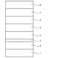
【解決手段】 1対の電極2,8の間に、ホール輸送層4、第1の発光層5、及び第2の発光層6が設けられており、第1の発光層5が少なくとも1つのドーパント材料とホスト材料を含み、ホスト材料として、ホール輸送層4のホール輸送性材料と同じ化合物が用いられている有機エレクトロルミネッセンス素子の製造方法において、ホール輸送層4と第1の発光層5を同一のチャンバー内で連続して形成することを特徴としている。
【選択図】 図1
Description
図1に示す構造を有する有機EL素子を作製した。図1を参照して、基板1の上には、ITOからなるホール注入電極が形成されており、ホール注入電極2の上には、NPBからなるホール輸送層4(厚み240nm)が設けられている。ホール輸送層4の上には、オレンジ色発光層5(厚み30nm)及び青色発光層6(厚み40nm)が設けられている。青色発光層6の上には、Alqからなる電子輸送層7(厚み30nm)が形成されている。電子輸送層7の上には、LiF(厚み1nm)とAl(厚み250nm)からなる電子注入電極8が設けられている。
表1に示すように、ホール輸送層及びオレンジ色発光層をチャンバーA内で連続して形成し、青色発光層及び電子輸送層をチャンバーB内で連続して形成した。
表1に示すように、ホール輸送層をチャンバーA内で形成し、オレンジ色発光層及び青色発光層をチャンバーB内で連続して形成し、電子輸送層をチャンバーC内で形成した。
表1に示すように、ホール輸送層をチャンバーA内で形成し、オレンジ色発光層をチャンバーB内で形成し、青色発光層及び電子輸送層をチャンバーC内で連続して形成した。
表1に示すように、ホール輸送層をチャンバーA内で形成し、オレンジ色発光層をチャンバーB内で形成し、青色発光層をチャンバーC内で形成し、電子輸送層をチャンバーD内で形成した。
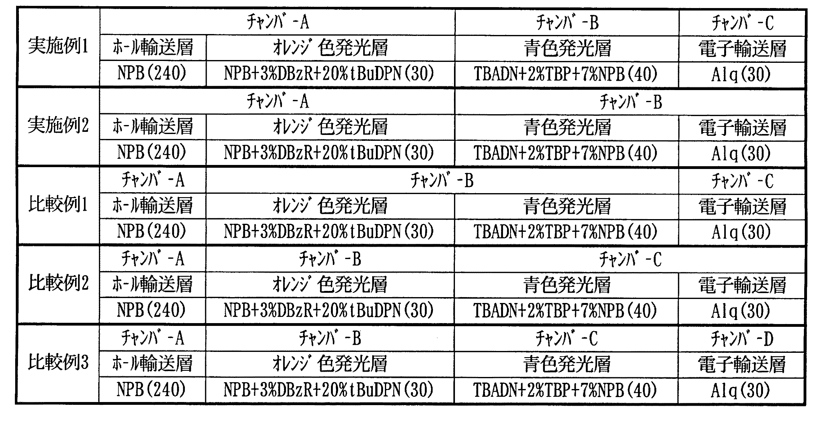
実施例1及び2並びに比較例1〜3の各有機EL素子について、発光効率、駆動電圧、及び寿命(半減期)を測定した。測定結果を表2に示す。
2…ホール注入電極
3…ホール注入層
4…ホール輸送層
5…オレンジ色発光層
6…青色発光層
7…電子輸送層
8…電子注入電極
Claims (4)
- 1対の電極の間に、ホール輸送層、第1の発光層、及び第2の発光層が設けられており、前記第1の発光層が少なくとも1つのドーパント材料とホスト材料を含み、該ホスト材料として、前記ホール輸送層のホール輸送性材料と同じ化合物が用いられている有機エレクトロルミネッセンス素子の製造方法において、
前記ホール輸送層と前記第1の発光層を同一チャンバー内で連続して形成することを特徴とする有機エレクトロルミネッセンス素子の製造方法。 - 前記第1の発光層がオレンジ色発光層であり、前記第2の発光層が青色発光層であることを特徴とする請求項1に記載の有機エレクトロルミネッセンス素子の製造方法。
- 前記ホール輸送層と前記第1の発光層を、真空蒸着法により蒸着源を変えることによって連続して形成することを特徴とする請求項1または2に記載の有機エレクトロルミネッセンス素子の製造方法。
- 前記ホール輸送性材料及び前記ホスト材料が、トリアリールアミン誘導体であることを特徴とする請求項1〜3のいずれか1項に記載の有機エレクトロルミネッセンス素子の製造方法。
Priority Applications (5)
| Application Number | Priority Date | Filing Date | Title |
|---|---|---|---|
| JP2004106377A JP2005293992A (ja) | 2004-03-31 | 2004-03-31 | 有機エレクトロルミネッセンス素子の製造方法 |
| TW094100015A TW200533235A (en) | 2004-03-31 | 2005-01-03 | Method for making organic electroluminescence element |
| KR1020050011835A KR20060041910A (ko) | 2004-03-31 | 2005-02-14 | 유기 전계 발광 소자의 제조 방법 |
| CNA2005100077659A CN1678142A (zh) | 2004-03-31 | 2005-02-16 | 有机电致发光元件的制造方法 |
| US11/085,233 US20060051497A1 (en) | 2004-03-31 | 2005-03-22 | Process for preparing organic electroluminescent device |
Applications Claiming Priority (1)
| Application Number | Priority Date | Filing Date | Title |
|---|---|---|---|
| JP2004106377A JP2005293992A (ja) | 2004-03-31 | 2004-03-31 | 有機エレクトロルミネッセンス素子の製造方法 |
Publications (1)
| Publication Number | Publication Date |
|---|---|
| JP2005293992A true JP2005293992A (ja) | 2005-10-20 |
Family
ID=35050384
Family Applications (1)
| Application Number | Title | Priority Date | Filing Date |
|---|---|---|---|
| JP2004106377A Pending JP2005293992A (ja) | 2004-03-31 | 2004-03-31 | 有機エレクトロルミネッセンス素子の製造方法 |
Country Status (5)
| Country | Link |
|---|---|
| US (1) | US20060051497A1 (ja) |
| JP (1) | JP2005293992A (ja) |
| KR (1) | KR20060041910A (ja) |
| CN (1) | CN1678142A (ja) |
| TW (1) | TW200533235A (ja) |
Cited By (3)
| Publication number | Priority date | Publication date | Assignee | Title |
|---|---|---|---|---|
| JP2007173779A (ja) * | 2005-12-20 | 2007-07-05 | Samsung Sdi Co Ltd | 有機電界発光表示素子およびその製造方法 |
| JP2007173780A (ja) * | 2005-12-20 | 2007-07-05 | Samsung Sdi Co Ltd | 有機発光表示素子及びその製造方法 |
| US7643750B2 (en) | 2005-10-20 | 2010-01-05 | Ricoh Company, Ltd. | Photographing apparatus with image-blur suppression mechanism |
Families Citing this family (7)
| Publication number | Priority date | Publication date | Assignee | Title |
|---|---|---|---|---|
| CN100484353C (zh) | 2008-01-29 | 2009-04-29 | 清华大学 | 有机电致发光器件 |
| KR101352116B1 (ko) | 2009-11-24 | 2014-01-14 | 엘지디스플레이 주식회사 | 백색 유기 발광 소자 |
| JP5703080B2 (ja) * | 2011-03-23 | 2015-04-15 | 株式会社東芝 | 有機電界発光素子、表示装置および照明装置 |
| JP6444046B2 (ja) * | 2013-04-03 | 2018-12-26 | キヤノン株式会社 | 有機化合物及び有機発光素子 |
| CN104505463A (zh) * | 2014-09-28 | 2015-04-08 | 桂林电子科技大学 | 一种双层发光层结构的白光oled器件 |
| CN105679957B (zh) * | 2016-04-20 | 2017-12-05 | 京东方科技集团股份有限公司 | 有机发光器件及其制备方法 |
| CN109599492A (zh) * | 2017-09-30 | 2019-04-09 | 昆山维信诺科技有限公司 | 发光器件 |
Family Cites Families (3)
| Publication number | Priority date | Publication date | Assignee | Title |
|---|---|---|---|---|
| US4234622A (en) * | 1979-04-11 | 1980-11-18 | The United States Of American As Represented By The Secretary Of The Army | Vacuum deposition method |
| US6501100B1 (en) * | 2000-05-15 | 2002-12-31 | General Electric Company | White light emitting phosphor blend for LED devices |
| US6929872B2 (en) * | 2000-10-05 | 2005-08-16 | Nippon Steel Chemical Co., Ltd. | Organic electroluminescent devices |
-
2004
- 2004-03-31 JP JP2004106377A patent/JP2005293992A/ja active Pending
-
2005
- 2005-01-03 TW TW094100015A patent/TW200533235A/zh unknown
- 2005-02-14 KR KR1020050011835A patent/KR20060041910A/ko not_active Withdrawn
- 2005-02-16 CN CNA2005100077659A patent/CN1678142A/zh active Pending
- 2005-03-22 US US11/085,233 patent/US20060051497A1/en not_active Abandoned
Cited By (3)
| Publication number | Priority date | Publication date | Assignee | Title |
|---|---|---|---|---|
| US7643750B2 (en) | 2005-10-20 | 2010-01-05 | Ricoh Company, Ltd. | Photographing apparatus with image-blur suppression mechanism |
| JP2007173779A (ja) * | 2005-12-20 | 2007-07-05 | Samsung Sdi Co Ltd | 有機電界発光表示素子およびその製造方法 |
| JP2007173780A (ja) * | 2005-12-20 | 2007-07-05 | Samsung Sdi Co Ltd | 有機発光表示素子及びその製造方法 |
Also Published As
| Publication number | Publication date |
|---|---|
| CN1678142A (zh) | 2005-10-05 |
| US20060051497A1 (en) | 2006-03-09 |
| TW200533235A (en) | 2005-10-01 |
| KR20060041910A (ko) | 2006-05-12 |
Similar Documents
| Publication | Publication Date | Title |
|---|---|---|
| JP4999291B2 (ja) | 有機エレクトロルミネッセンス素子およびそれを備える表示装置又は発光装置 | |
| TW546851B (en) | Organic light-emitting device having a color-neutral dopant in a hole-transport layer and/or in an electron-transport layer | |
| US6475648B1 (en) | Organic electroluminescent devices with improved stability and efficiency | |
| JP4011325B2 (ja) | 有機エレクトロルミネッセンス素子 | |
| JP4785386B2 (ja) | 有機エレクトロルミネッセント素子及び有機エレクトロルミネッセント表示装置 | |
| KR20030014119A (ko) | 방출층 및 정공 수송층 중에 색 중성 도펀트를 갖는 유기발광장치 | |
| JP2003115387A (ja) | 有機発光素子及びその製造方法 | |
| JP3577117B2 (ja) | 有機エレクトロルミネセンス素子の製法 | |
| TW200401584A (en) | White organic light-emitting devices using rubrene layer | |
| JP2016219853A (ja) | 発光素子 | |
| JP2012186467A (ja) | 発光体、発光層、発光素子および発光装置 | |
| WO2002099008A1 (en) | Organo-electroluminescence element, luminescent material and organic compound | |
| WO2002064700A1 (fr) | Dispositif d'electroluminescence organique, materiau luminescent, et compose organique | |
| JP4721668B2 (ja) | 有機エレクトロルミネッセンス素子 | |
| EP3451401B1 (en) | Oled device and method for manufacturing same, and oled display panel | |
| JP2005293992A (ja) | 有機エレクトロルミネッセンス素子の製造方法 | |
| JP2007179933A (ja) | 有機エレクトロルミネッセント素子及び有機エレクトロルミネッセント表示装置 | |
| JP3825725B2 (ja) | 有機エレクトロルミネッセンス素子 | |
| CN1914956A (zh) | 有机电致发光元件 | |
| Lee et al. | Host-free, yellow phosphorescent material in white organic light-emitting diodes | |
| JP2007318130A (ja) | 有機発光デバイス、発光層、およびその製造方法 | |
| JP4578215B2 (ja) | 有機エレクトロルミネッセント素子及び有機エレクトロルミネッセント表示装置 | |
| JP4214482B2 (ja) | 有機エレクトロルミネッセンス素子 | |
| JP2006073642A (ja) | 有機エレクトロルミネッセンス素子およびそれを備える有機エレクトロルミネッセンス装置 | |
| JP2006210747A (ja) | 有機エレクトロルミネッセンス素子 |
Legal Events
| Date | Code | Title | Description |
|---|---|---|---|
| A621 | Written request for application examination |
Free format text: JAPANESE INTERMEDIATE CODE: A621 Effective date: 20050719 |
|
| A977 | Report on retrieval |
Free format text: JAPANESE INTERMEDIATE CODE: A971007 Effective date: 20071011 |
|
| A131 | Notification of reasons for refusal |
Free format text: JAPANESE INTERMEDIATE CODE: A131 Effective date: 20071023 |
|
| A521 | Request for written amendment filed |
Free format text: JAPANESE INTERMEDIATE CODE: A523 Effective date: 20071225 |
|
| A131 | Notification of reasons for refusal |
Free format text: JAPANESE INTERMEDIATE CODE: A131 Effective date: 20080401 |
|
| A521 | Request for written amendment filed |
Free format text: JAPANESE INTERMEDIATE CODE: A523 Effective date: 20080602 |
|
| A02 | Decision of refusal |
Free format text: JAPANESE INTERMEDIATE CODE: A02 Effective date: 20080909 |