JP2005293992A - Manufacturing method of organic electroluminescent element - Google Patents
Manufacturing method of organic electroluminescent element Download PDFInfo
- Publication number
- JP2005293992A JP2005293992A JP2004106377A JP2004106377A JP2005293992A JP 2005293992 A JP2005293992 A JP 2005293992A JP 2004106377 A JP2004106377 A JP 2004106377A JP 2004106377 A JP2004106377 A JP 2004106377A JP 2005293992 A JP2005293992 A JP 2005293992A
- Authority
- JP
- Japan
- Prior art keywords
- emitting layer
- light emitting
- hole transport
- layer
- transport layer
- Prior art date
- Legal status (The legal status is an assumption and is not a legal conclusion. Google has not performed a legal analysis and makes no representation as to the accuracy of the status listed.)
- Pending
Links
- 238000004519 manufacturing process Methods 0.000 title claims abstract description 11
- 230000005525 hole transport Effects 0.000 claims abstract description 32
- 239000000463 material Substances 0.000 claims abstract description 31
- 239000002019 doping agent Substances 0.000 claims abstract description 9
- 150000001875 compounds Chemical class 0.000 claims abstract description 7
- 238000009751 slip forming Methods 0.000 claims description 7
- 238000005401 electroluminescence Methods 0.000 claims description 5
- 238000001771 vacuum deposition Methods 0.000 claims description 4
- 238000000151 deposition Methods 0.000 claims description 3
- 230000008021 deposition Effects 0.000 claims description 3
- 238000000034 method Methods 0.000 claims description 3
- 125000005259 triarylamine group Chemical group 0.000 claims description 3
- 238000002347 injection Methods 0.000 description 9
- 239000007924 injection Substances 0.000 description 9
- 230000000052 comparative effect Effects 0.000 description 6
- 239000011368 organic material Substances 0.000 description 6
- 230000015572 biosynthetic process Effects 0.000 description 4
- OBAJPWYDYFEBTF-UHFFFAOYSA-N 2-tert-butyl-9,10-dinaphthalen-2-ylanthracene Chemical compound C1=CC=CC2=CC(C3=C4C=CC=CC4=C(C=4C=C5C=CC=CC5=CC=4)C4=CC=C(C=C43)C(C)(C)C)=CC=C21 OBAJPWYDYFEBTF-UHFFFAOYSA-N 0.000 description 3
- QVGXLLKOCUKJST-UHFFFAOYSA-N atomic oxygen Chemical compound [O] QVGXLLKOCUKJST-UHFFFAOYSA-N 0.000 description 3
- 229910052760 oxygen Inorganic materials 0.000 description 3
- 239000001301 oxygen Substances 0.000 description 3
- XLYOFNOQVPJJNP-UHFFFAOYSA-N water Substances O XLYOFNOQVPJJNP-UHFFFAOYSA-N 0.000 description 3
- -1 arylamine compound Chemical class 0.000 description 2
- 230000005281 excited state Effects 0.000 description 2
- 239000000758 substrate Substances 0.000 description 2
- 238000007740 vapor deposition Methods 0.000 description 2
- BFTIPCRZWILUIY-UHFFFAOYSA-N 2,5,8,11-tetratert-butylperylene Chemical group CC(C)(C)C1=CC(C2=CC(C(C)(C)C)=CC=3C2=C2C=C(C=3)C(C)(C)C)=C3C2=CC(C(C)(C)C)=CC3=C1 BFTIPCRZWILUIY-UHFFFAOYSA-N 0.000 description 1
- ZVYVRXAIGFRABK-UHFFFAOYSA-N 5,12-bis(4-tert-butylphenyl)tetracene Chemical compound C1=CC(C(C)(C)C)=CC=C1C(C1=CC2=CC=CC=C2C=C11)=C(C=CC=C2)C2=C1C1=CC=C(C(C)(C)C)C=C1 ZVYVRXAIGFRABK-UHFFFAOYSA-N 0.000 description 1
- WTCSROCYPKJPDZ-UHFFFAOYSA-N 6-methyl-2-[4-[12-[4-(6-methyl-1,3-benzothiazol-2-yl)phenyl]-6,11-diphenyltetracen-5-yl]phenyl]-1,3-benzothiazole Chemical group S1C2=CC(C)=CC=C2N=C1C(C=C1)=CC=C1C(C1=C(C=2C=CC=CC=2)C2=CC=CC=C22)=C3C=CC=CC3=C(C=3C=CC(=CC=3)C=3SC4=CC(C)=CC=C4N=3)C1=C2C1=CC=CC=C1 WTCSROCYPKJPDZ-UHFFFAOYSA-N 0.000 description 1
- REDXJYDRNCIFBQ-UHFFFAOYSA-N aluminium(3+) Chemical compound [Al+3] REDXJYDRNCIFBQ-UHFFFAOYSA-N 0.000 description 1
- 238000006243 chemical reaction Methods 0.000 description 1
- 230000000694 effects Effects 0.000 description 1
- 238000011156 evaluation Methods 0.000 description 1
- 230000005284 excitation Effects 0.000 description 1
- 230000002349 favourable effect Effects 0.000 description 1
- 238000004020 luminiscence type Methods 0.000 description 1
- 238000005259 measurement Methods 0.000 description 1
- IBHBKWKFFTZAHE-UHFFFAOYSA-N n-[4-[4-(n-naphthalen-1-ylanilino)phenyl]phenyl]-n-phenylnaphthalen-1-amine Chemical group C1=CC=CC=C1N(C=1C2=CC=CC=C2C=CC=1)C1=CC=C(C=2C=CC(=CC=2)N(C=2C=CC=CC=2)C=2C3=CC=CC=C3C=CC=2)C=C1 IBHBKWKFFTZAHE-UHFFFAOYSA-N 0.000 description 1
- 238000005268 plasma chemical vapour deposition Methods 0.000 description 1
- 238000001179 sorption measurement Methods 0.000 description 1
- 238000007738 vacuum evaporation Methods 0.000 description 1
Images
Classifications
-
- H—ELECTRICITY
- H05—ELECTRIC TECHNIQUES NOT OTHERWISE PROVIDED FOR
- H05B—ELECTRIC HEATING; ELECTRIC LIGHT SOURCES NOT OTHERWISE PROVIDED FOR; CIRCUIT ARRANGEMENTS FOR ELECTRIC LIGHT SOURCES, IN GENERAL
- H05B33/00—Electroluminescent light sources
- H05B33/10—Apparatus or processes specially adapted to the manufacture of electroluminescent light sources
-
- C—CHEMISTRY; METALLURGY
- C09—DYES; PAINTS; POLISHES; NATURAL RESINS; ADHESIVES; COMPOSITIONS NOT OTHERWISE PROVIDED FOR; APPLICATIONS OF MATERIALS NOT OTHERWISE PROVIDED FOR
- C09K—MATERIALS FOR MISCELLANEOUS APPLICATIONS, NOT PROVIDED FOR ELSEWHERE
- C09K11/00—Luminescent, e.g. electroluminescent, chemiluminescent materials
- C09K11/06—Luminescent, e.g. electroluminescent, chemiluminescent materials containing organic luminescent materials
-
- H—ELECTRICITY
- H05—ELECTRIC TECHNIQUES NOT OTHERWISE PROVIDED FOR
- H05B—ELECTRIC HEATING; ELECTRIC LIGHT SOURCES NOT OTHERWISE PROVIDED FOR; CIRCUIT ARRANGEMENTS FOR ELECTRIC LIGHT SOURCES, IN GENERAL
- H05B33/00—Electroluminescent light sources
- H05B33/12—Light sources with substantially two-dimensional radiating surfaces
- H05B33/14—Light sources with substantially two-dimensional radiating surfaces characterised by the chemical or physical composition or the arrangement of the electroluminescent material, or by the simultaneous addition of the electroluminescent material in or onto the light source
-
- H—ELECTRICITY
- H10—SEMICONDUCTOR DEVICES; ELECTRIC SOLID-STATE DEVICES NOT OTHERWISE PROVIDED FOR
- H10K—ORGANIC ELECTRIC SOLID-STATE DEVICES
- H10K50/00—Organic light-emitting devices
- H10K50/10—OLEDs or polymer light-emitting diodes [PLED]
- H10K50/11—OLEDs or polymer light-emitting diodes [PLED] characterised by the electroluminescent [EL] layers
- H10K50/125—OLEDs or polymer light-emitting diodes [PLED] characterised by the electroluminescent [EL] layers specially adapted for multicolour light emission, e.g. for emitting white light
-
- H—ELECTRICITY
- H10—SEMICONDUCTOR DEVICES; ELECTRIC SOLID-STATE DEVICES NOT OTHERWISE PROVIDED FOR
- H10K—ORGANIC ELECTRIC SOLID-STATE DEVICES
- H10K71/00—Manufacture or treatment specially adapted for the organic devices covered by this subclass
- H10K71/10—Deposition of organic active material
- H10K71/16—Deposition of organic active material using physical vapour deposition [PVD], e.g. vacuum deposition or sputtering
-
- H—ELECTRICITY
- H10—SEMICONDUCTOR DEVICES; ELECTRIC SOLID-STATE DEVICES NOT OTHERWISE PROVIDED FOR
- H10K—ORGANIC ELECTRIC SOLID-STATE DEVICES
- H10K85/00—Organic materials used in the body or electrodes of devices covered by this subclass
- H10K85/60—Organic compounds having low molecular weight
- H10K85/615—Polycyclic condensed aromatic hydrocarbons, e.g. anthracene
- H10K85/622—Polycyclic condensed aromatic hydrocarbons, e.g. anthracene containing four rings, e.g. pyrene
-
- H—ELECTRICITY
- H10—SEMICONDUCTOR DEVICES; ELECTRIC SOLID-STATE DEVICES NOT OTHERWISE PROVIDED FOR
- H10K—ORGANIC ELECTRIC SOLID-STATE DEVICES
- H10K85/00—Organic materials used in the body or electrodes of devices covered by this subclass
- H10K85/60—Organic compounds having low molecular weight
- H10K85/649—Aromatic compounds comprising a hetero atom
- H10K85/657—Polycyclic condensed heteroaromatic hydrocarbons
-
- C—CHEMISTRY; METALLURGY
- C09—DYES; PAINTS; POLISHES; NATURAL RESINS; ADHESIVES; COMPOSITIONS NOT OTHERWISE PROVIDED FOR; APPLICATIONS OF MATERIALS NOT OTHERWISE PROVIDED FOR
- C09K—MATERIALS FOR MISCELLANEOUS APPLICATIONS, NOT PROVIDED FOR ELSEWHERE
- C09K2211/00—Chemical nature of organic luminescent or tenebrescent compounds
- C09K2211/10—Non-macromolecular compounds
- C09K2211/1003—Carbocyclic compounds
- C09K2211/1011—Condensed systems
-
- H—ELECTRICITY
- H10—SEMICONDUCTOR DEVICES; ELECTRIC SOLID-STATE DEVICES NOT OTHERWISE PROVIDED FOR
- H10K—ORGANIC ELECTRIC SOLID-STATE DEVICES
- H10K2102/00—Constructional details relating to the organic devices covered by this subclass
- H10K2102/10—Transparent electrodes, e.g. using graphene
- H10K2102/101—Transparent electrodes, e.g. using graphene comprising transparent conductive oxides [TCO]
- H10K2102/103—Transparent electrodes, e.g. using graphene comprising transparent conductive oxides [TCO] comprising indium oxides, e.g. ITO
-
- H—ELECTRICITY
- H10—SEMICONDUCTOR DEVICES; ELECTRIC SOLID-STATE DEVICES NOT OTHERWISE PROVIDED FOR
- H10K—ORGANIC ELECTRIC SOLID-STATE DEVICES
- H10K71/00—Manufacture or treatment specially adapted for the organic devices covered by this subclass
-
- H—ELECTRICITY
- H10—SEMICONDUCTOR DEVICES; ELECTRIC SOLID-STATE DEVICES NOT OTHERWISE PROVIDED FOR
- H10K—ORGANIC ELECTRIC SOLID-STATE DEVICES
- H10K85/00—Organic materials used in the body or electrodes of devices covered by this subclass
- H10K85/30—Coordination compounds
- H10K85/321—Metal complexes comprising a group IIIA element, e.g. Tris (8-hydroxyquinoline) gallium [Gaq3]
- H10K85/324—Metal complexes comprising a group IIIA element, e.g. Tris (8-hydroxyquinoline) gallium [Gaq3] comprising aluminium, e.g. Alq3
-
- H—ELECTRICITY
- H10—SEMICONDUCTOR DEVICES; ELECTRIC SOLID-STATE DEVICES NOT OTHERWISE PROVIDED FOR
- H10K—ORGANIC ELECTRIC SOLID-STATE DEVICES
- H10K85/00—Organic materials used in the body or electrodes of devices covered by this subclass
- H10K85/60—Organic compounds having low molecular weight
- H10K85/615—Polycyclic condensed aromatic hydrocarbons, e.g. anthracene
- H10K85/626—Polycyclic condensed aromatic hydrocarbons, e.g. anthracene containing more than one polycyclic condensed aromatic rings, e.g. bis-anthracene
-
- H—ELECTRICITY
- H10—SEMICONDUCTOR DEVICES; ELECTRIC SOLID-STATE DEVICES NOT OTHERWISE PROVIDED FOR
- H10K—ORGANIC ELECTRIC SOLID-STATE DEVICES
- H10K85/00—Organic materials used in the body or electrodes of devices covered by this subclass
- H10K85/60—Organic compounds having low molecular weight
- H10K85/631—Amine compounds having at least two aryl rest on at least one amine-nitrogen atom, e.g. triphenylamine
Abstract
Description
本発明は、有機エレクトロルミネッセンス素子の製造方法に関するものである。 The present invention relates to a method for manufacturing an organic electroluminescence element.
有機エレクトロルミネッセンス素子(有機EL素子)は、ディスプレイや照明への応用の観点から活発に開発が行われている。有機EL素子の駆動原理は、以下のようなものである。すなわち、ホール注入電極及び電子注入電極からそれぞれホールと電子が注入され、これらが有機材料からなるキャリア輸送層中などを輸送され、発光層において再結合しこれによって発光材料に励起状態が生じ、この励起状態から発光が得られる。 Organic electroluminescence elements (organic EL elements) have been actively developed from the viewpoint of application to displays and lighting. The driving principle of the organic EL element is as follows. That is, holes and electrons are injected from the hole injection electrode and the electron injection electrode, respectively, are transported in a carrier transport layer made of an organic material, and recombined in the light emitting layer, thereby generating an excited state in the light emitting material. Luminescence is obtained from the excited state.
発光層を、ホスト材料と発光性のドーパント材料から形成し、ホスト材料からの励起エネルギーを発光性ドーパントに効率良く移動させることにより、発光効率を高めた有機EL素子が提案されている(特許文献1など)。また、発光層として、青色発光層とオレンジ色発光層を配置し、白色発光の有機EL素子とすることも試みられている。 There has been proposed an organic EL element having a luminous efficiency enhanced by forming a light emitting layer from a host material and a light emitting dopant material and efficiently transferring excitation energy from the host material to the light emitting dopant (Patent Literature). 1). Further, an attempt has been made to arrange a blue light-emitting layer and an orange light-emitting layer as a light-emitting layer to obtain a white light-emitting organic EL element.
発光層及びキャリア輸送層などの有機材料層は、一般に真空蒸着法により形成されている。真空蒸着法による各層の形成は、一般にチャンバー内で行われているが、複数の層を同一チャンバー内で形成することや、どのような層を同一チャンバー内で形成することが好ましいかなどについて詳細には検討されていない。
本発明の目的は、寿命特性を著しく向上させることができる有機EL素子の製造方法を提供することにある。 The objective of this invention is providing the manufacturing method of the organic EL element which can improve a lifetime characteristic remarkably.
本発明は、1対の電極の間に、ホール輸送層、第1の発光層、及び第2の発光層が設けられており、該第1の発光層が少なくとも1つのドーパント材料とホスト材料を含み、該ホスト材料として、ホール輸送層のホール輸送性材料と同じ化合物が用いられている有機EL素子の製造方法であり、ホール輸送層と第1の発光層を同一チャンバー内で連続して形成することを特徴としている。 In the present invention, a hole transport layer, a first light-emitting layer, and a second light-emitting layer are provided between a pair of electrodes, and the first light-emitting layer includes at least one dopant material and a host material. And a method of manufacturing an organic EL device in which the same compound as the hole transporting material of the hole transporting layer is used as the host material, and the hole transporting layer and the first light emitting layer are continuously formed in the same chamber. It is characterized by doing.
本発明の有機EL素子においては、第1の発光層に含まれるホスト材料として、ホール輸送層のホール輸送性材料と同じ化合物が用いられている。本発明においては、このように同じ化合物が用いられているホール輸送層と第1の発光層とを同一のチャンバー内で連続して形成している。ホール輸送層と第1の発光層を同一のチャンバー内で連続して形成することにより、驚くべきことに、有機EL素子の発光寿命特性を著しく向上させることができる。 In the organic EL device of the present invention, the same compound as the hole transporting material of the hole transporting layer is used as the host material contained in the first light emitting layer. In the present invention, the hole transport layer and the first light emitting layer in which the same compound is used are continuously formed in the same chamber. By forming the hole transport layer and the first light emitting layer continuously in the same chamber, it is surprising that the light emission lifetime characteristics of the organic EL element can be remarkably improved.
本発明において、ホール輸送層と第1の発光層を同一チャンバー内で連続して形成することにより、良好な寿命特性が得られる理由について、詳細は明らかではないが、同一のチャンバー内で連続して形成することにより、ホール輸送層と第1の発光層の界面が良好な状態で形成されるため、発光層及びホール輸送層における有機材料の劣化が生じにくくなっているものと思われる。すなわち、本発明においては、トリアリールアミン系化合物であるNPBに代表されるアリールアミン系化合物などのホール輸送性材料がホール輸送層及び第1の発光層に含有されているが、これらのホール輸送性材料は表面に吸着する酸素や水等の影響を受けやすい。このため、ホール輸送層と第1の発光層の界面に酸素や水等が吸着すると、界面において相変化が生じやすく、このため化学反応により有機材料が変化してしまうおそれがある。本発明に従い、ホール輸送層と第1の発光層を同一チャンバー内で連続して形成することにより、このような界面における酸素や水等の吸着を防止することができるので、発光層及びホール輸送層における有機材料の劣化が生じにくくなるものと思われる。 In the present invention, the reason why good lifetime characteristics can be obtained by continuously forming the hole transport layer and the first light emitting layer in the same chamber is not clear in detail, but it is continuous in the same chamber. It is considered that since the interface between the hole transport layer and the first light emitting layer is formed in a favorable state, the organic material in the light emitting layer and the hole transport layer is hardly deteriorated. That is, in the present invention, a hole transporting material such as an arylamine compound represented by NPB, which is a triarylamine compound, is contained in the hole transport layer and the first light emitting layer. The material is easily affected by oxygen or water adsorbed on the surface. For this reason, when oxygen, water, or the like is adsorbed on the interface between the hole transport layer and the first light-emitting layer, a phase change is likely to occur at the interface, and the organic material may change due to a chemical reaction. According to the present invention, by continuously forming the hole transport layer and the first light emitting layer in the same chamber, it is possible to prevent adsorption of oxygen, water, and the like at such an interface. It seems that the organic material in the layer is less likely to deteriorate.
本発明においては、第1の発光層としてオレンジ色発光層を形成し、第2の発光層として青色発光層を形成することにより、白色発光の有機EL素子とすることができる。オレンジ色発光層においては、ホスト材料としてトリアリールアミン誘導体を用いることができ、このトリアリールアミン誘導体はホール輸送性材料であるので、これを用いてホール輸送層を形成することができる。 In the present invention, by forming an orange light emitting layer as the first light emitting layer and forming a blue light emitting layer as the second light emitting layer, a white light emitting organic EL element can be obtained. In the orange light emitting layer, a triarylamine derivative can be used as a host material, and since this triarylamine derivative is a hole transporting material, it can be used to form a hole transport layer.
本発明においては、ホール輸送層と第1の発光層が、同一のチャンバー内で連続して形成される。真空蒸着法によりこれらの層を形成する場合、チャンバー内での蒸着源の蓋の開閉により、蒸着源を変えて形成することができる。この場合、ホスト材料とホール輸送性材料は同じ化合物であるので、これらの化合物の蒸着源として、同一の蒸着源を用いてもよい。 In the present invention, the hole transport layer and the first light emitting layer are continuously formed in the same chamber. When these layers are formed by vacuum deposition, the deposition source can be changed by opening and closing the lid of the deposition source in the chamber. In this case, since the host material and the hole transport material are the same compound, the same vapor deposition source may be used as the vapor deposition source of these compounds.
本発明に従い、ホール輸送層と第1の発光層を同一チャンバー内で連続して形成することにより、寿命特性に優れた有機EL素子を製造することができる。 According to the present invention, by continuously forming the hole transport layer and the first light emitting layer in the same chamber, an organic EL device having excellent lifetime characteristics can be produced.
以下、本発明を実施例により具体的に説明するが、本発明は以下の実施例に限定されるものではない。 EXAMPLES Hereinafter, although an Example demonstrates this invention concretely, this invention is not limited to a following example.
(実施例1)
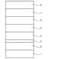
図1に示す構造を有する有機EL素子を作製した。図1を参照して、基板1の上には、ITOからなるホール注入電極が形成されており、ホール注入電極2の上には、NPBからなるホール輸送層4(厚み240nm)が設けられている。ホール輸送層4の上には、オレンジ色発光層5(厚み30nm)及び青色発光層6(厚み40nm)が設けられている。青色発光層6の上には、Alqからなる電子輸送層7(厚み30nm)が形成されている。電子輸送層7の上には、LiF(厚み1nm)とAl(厚み250nm)からなる電子注入電極8が設けられている。
(Example 1)
An organic EL element having the structure shown in FIG. 1 was produced. Referring to FIG. 1, a hole injection electrode made of ITO is formed on a substrate 1, and a hole transport layer 4 (thickness 240 nm) made of NPB is provided on
オレンジ色発光層5は、NPBをホスト材料として用い、3重量%のDBzRを発光性ドーパント材料として用い、20重量%のtBuDPNをキャリア輸送性ドーパントとして用いている。
The orange
青色発光層6は、TBADNをホスト材料として用い、2重量%のTBPを発光性ドーパント材料として用い、7重量%のNPBをキャリア輸送性ドーパント材料として用いている。
The blue
CFxからなるホール注入層3は、プラズマCVD法により形成した。それ以外の各層は、真空蒸着法により形成した。
The
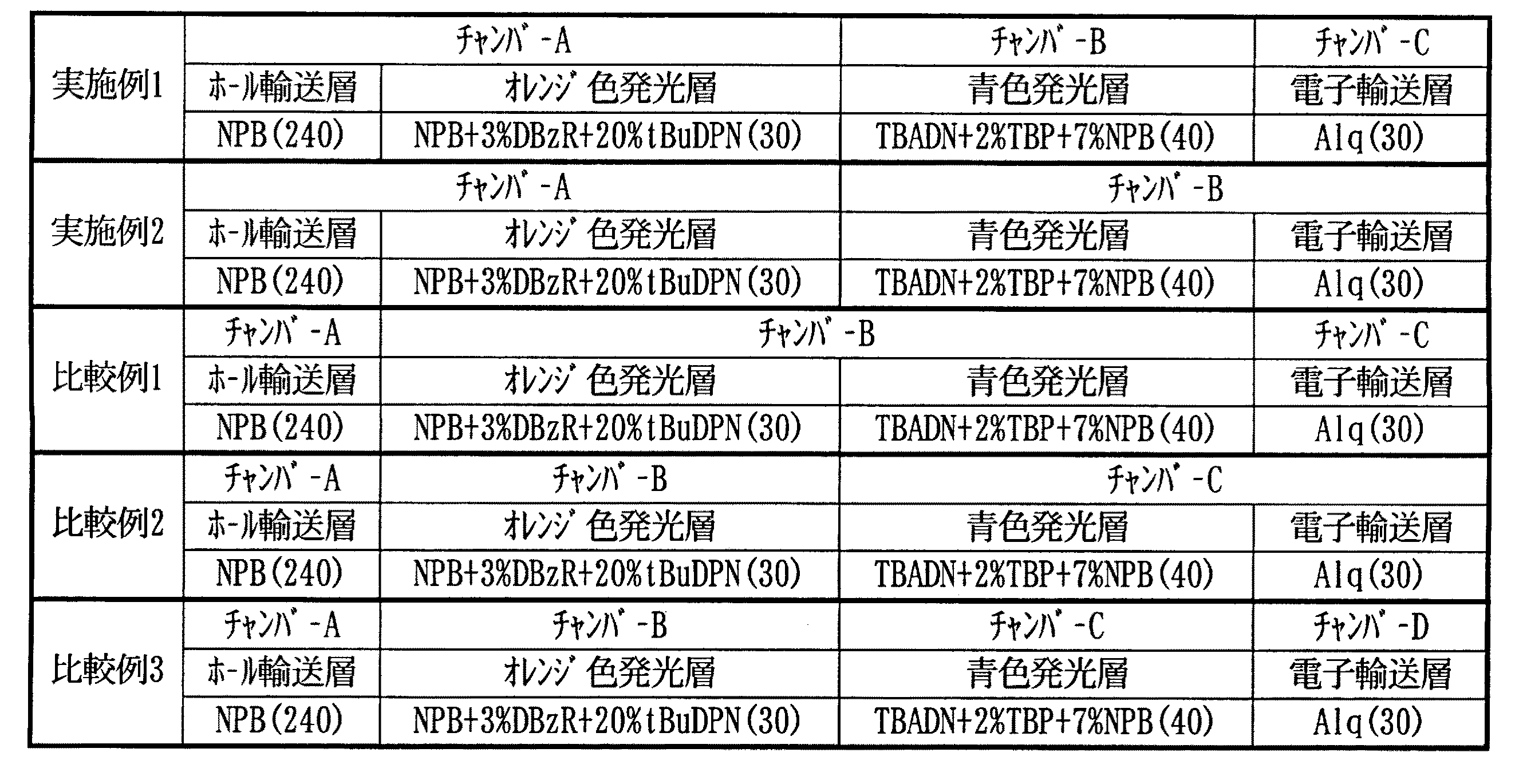
表1に示すように、ホール輸送層4及びオレンジ色発光層5は、チャンバーA内で連続して形成した。青色発光層6はチャンバーB内で形成し、電子輸送層7はチャンバーC内で形成した。
As shown in Table 1, the
(実施例2)
表1に示すように、ホール輸送層及びオレンジ色発光層をチャンバーA内で連続して形成し、青色発光層及び電子輸送層をチャンバーB内で連続して形成した。
(Example 2)
As shown in Table 1, a hole transport layer and an orange light emitting layer were formed continuously in the chamber A, and a blue light emitting layer and an electron transport layer were formed continuously in the chamber B.
(比較例1)
表1に示すように、ホール輸送層をチャンバーA内で形成し、オレンジ色発光層及び青色発光層をチャンバーB内で連続して形成し、電子輸送層をチャンバーC内で形成した。
(Comparative Example 1)
As shown in Table 1, a hole transport layer was formed in chamber A, an orange light-emitting layer and a blue light-emitting layer were formed continuously in chamber B, and an electron transport layer was formed in chamber C.
(比較例2)
表1に示すように、ホール輸送層をチャンバーA内で形成し、オレンジ色発光層をチャンバーB内で形成し、青色発光層及び電子輸送層をチャンバーC内で連続して形成した。
(Comparative Example 2)
As shown in Table 1, a hole transport layer was formed in chamber A, an orange light-emitting layer was formed in chamber B, and a blue light-emitting layer and an electron transport layer were formed continuously in chamber C.
(比較例3)
表1に示すように、ホール輸送層をチャンバーA内で形成し、オレンジ色発光層をチャンバーB内で形成し、青色発光層をチャンバーC内で形成し、電子輸送層をチャンバーD内で形成した。
(Comparative Example 3)
As shown in Table 1, a hole transport layer is formed in chamber A, an orange light emitting layer is formed in chamber B, a blue light emitting layer is formed in chamber C, and an electron transport layer is formed in chamber D. did.
各層の形成に用いた有機材料は、以下の通りである。 The organic materials used for forming each layer are as follows.
NPBは、N,N′−ジ(1−ナフチル)−N,N′−ジフェニルベンジジンであり、以下の構造を有している。 NPB is N, N′-di (1-naphthyl) -N, N′-diphenylbenzidine and has the following structure.
DBzRは、5,12−ビス{4−(6−メチルベンゾチアゾール−2−イル)フェニル}−6,11−ジフェニルナフタセンであり、以下の構造を有している。 DBzR is 5,12-bis {4- (6-methylbenzothiazol-2-yl) phenyl} -6,11-diphenylnaphthacene and has the following structure.
tBuDPNは、5,12−ビス(4−ターシャリー−ブチルフェニル)ナフタセンであり、以下の構造を有している。 tBuDPN is 5,12-bis (4-tertiary-butylphenyl) naphthacene and has the following structure.
TBADNは、2−ターシャリー−ブチル−9,10−ジ(2−ナフチル)アントラセンであり、以下の構造を有している。 TBADN is 2-tertiary-butyl-9,10-di (2-naphthyl) anthracene and has the following structure.
TBPは、2,5,8,11−テトラ−ターシャリー−ブチルペリレンであり、以下の構造を有している。 TBP is 2,5,8,11-tetra-tertiary-butylperylene and has the following structure.
Alqは、トリス−(8−キノリラト)アルミニウム(III)であり、以下の構造を有している。 Alq is tris- (8-quinolinato) aluminum (III) and has the following structure.
〔有機EL素子の評価〕
実施例1及び2並びに比較例1〜3の各有機EL素子について、発光効率、駆動電圧、及び寿命(半減期)を測定した。測定結果を表2に示す。
[Evaluation of organic EL elements]
About each organic EL element of Examples 1 and 2 and Comparative Examples 1-3, luminous efficiency, drive voltage, and lifetime (half-life) were measured. The measurement results are shown in Table 2.
表2に示す結果から明らかなように、本発明に従いホール輸送層及びオレンジ色発光層を同一チャンバーA内で連続して形成した実施例1及び2の有機EL素子は、比較例1〜3の有機EL素子に比べ、2倍以上長い寿命特性を示している。比較例1〜3との比較から明らかなように、オレンジ色発光層と青色発光層の連続形成や、青色発光層と電子輸送層の連続形成では、本発明の効果が得られておらず、ホール輸送層とオレンジ色発光層を連続形成した場合にのみ特異的に寿命特性が向上することがわかる。 As is clear from the results shown in Table 2, the organic EL devices of Examples 1 and 2 in which the hole transport layer and the orange light emitting layer were continuously formed in the same chamber A in accordance with the present invention were those of Comparative Examples 1 to 3. Compared to organic EL elements, it has a lifetime characteristic that is at least twice as long. As is clear from the comparison with Comparative Examples 1 to 3, the continuous formation of the orange light-emitting layer and the blue light-emitting layer, and the continuous formation of the blue light-emitting layer and the electron transport layer, the effect of the present invention has not been obtained, It can be seen that the lifetime characteristics are specifically improved only when the hole transport layer and the orange light emitting layer are continuously formed.
1…基板
2…ホール注入電極
3…ホール注入層
4…ホール輸送層
5…オレンジ色発光層
6…青色発光層
7…電子輸送層
8…電子注入電極
DESCRIPTION OF SYMBOLS 1 ...
Claims (4)
前記ホール輸送層と前記第1の発光層を同一チャンバー内で連続して形成することを特徴とする有機エレクトロルミネッセンス素子の製造方法。 A hole transport layer, a first light-emitting layer, and a second light-emitting layer are provided between the pair of electrodes, and the first light-emitting layer includes at least one dopant material and a host material, and the host In the method of manufacturing an organic electroluminescence device in which the same compound as the hole transport material of the hole transport layer is used as a material,
The method of manufacturing an organic electroluminescence element, wherein the hole transport layer and the first light emitting layer are continuously formed in the same chamber.
The method for producing an organic electroluminescent element according to claim 1, wherein the hole transporting material and the host material are triarylamine derivatives.
Priority Applications (5)
| Application Number | Priority Date | Filing Date | Title |
|---|---|---|---|
| JP2004106377A JP2005293992A (en) | 2004-03-31 | 2004-03-31 | Manufacturing method of organic electroluminescent element |
| TW094100015A TW200533235A (en) | 2004-03-31 | 2005-01-03 | Method for making organic electroluminescence element |
| KR1020050011835A KR20060041910A (en) | 2004-03-31 | 2005-02-14 | Fabrication method of organic electroluminescent device |
| CNA2005100077659A CN1678142A (en) | 2004-03-31 | 2005-02-16 | Organic electroluminescence element mfg. method |
| US11/085,233 US20060051497A1 (en) | 2004-03-31 | 2005-03-22 | Process for preparing organic electroluminescent device |
Applications Claiming Priority (1)
| Application Number | Priority Date | Filing Date | Title |
|---|---|---|---|
| JP2004106377A JP2005293992A (en) | 2004-03-31 | 2004-03-31 | Manufacturing method of organic electroluminescent element |
Publications (1)
| Publication Number | Publication Date |
|---|---|
| JP2005293992A true JP2005293992A (en) | 2005-10-20 |
Family
ID=35050384
Family Applications (1)
| Application Number | Title | Priority Date | Filing Date |
|---|---|---|---|
| JP2004106377A Pending JP2005293992A (en) | 2004-03-31 | 2004-03-31 | Manufacturing method of organic electroluminescent element |
Country Status (5)
| Country | Link |
|---|---|
| US (1) | US20060051497A1 (en) |
| JP (1) | JP2005293992A (en) |
| KR (1) | KR20060041910A (en) |
| CN (1) | CN1678142A (en) |
| TW (1) | TW200533235A (en) |
Cited By (3)
| Publication number | Priority date | Publication date | Assignee | Title |
|---|---|---|---|---|
| JP2007173779A (en) * | 2005-12-20 | 2007-07-05 | Samsung Sdi Co Ltd | Organic electroluminescent display element and manufacturing method thereof |
| JP2007173780A (en) * | 2005-12-20 | 2007-07-05 | Samsung Sdi Co Ltd | Organic electroluminescent display element and manufacturing method thereof |
| US7643750B2 (en) | 2005-10-20 | 2010-01-05 | Ricoh Company, Ltd. | Photographing apparatus with image-blur suppression mechanism |
Families Citing this family (7)
| Publication number | Priority date | Publication date | Assignee | Title |
|---|---|---|---|---|
| CN100484353C (en) | 2008-01-29 | 2009-04-29 | 清华大学 | Organic electroluminescent part |
| KR101352116B1 (en) * | 2009-11-24 | 2014-01-14 | 엘지디스플레이 주식회사 | White Organic Light Emitting Device |
| JP5703080B2 (en) * | 2011-03-23 | 2015-04-15 | 株式会社東芝 | Organic electroluminescent element, display device and lighting device |
| JP6444046B2 (en) * | 2013-04-03 | 2018-12-26 | キヤノン株式会社 | Organic compound and organic light emitting device |
| CN104505463A (en) * | 2014-09-28 | 2015-04-08 | 桂林电子科技大学 | White light OLED (organic light emitting diode) device with double-layer light emitting layer structure |
| CN105679957B (en) * | 2016-04-20 | 2017-12-05 | 京东方科技集团股份有限公司 | Organic luminescent device and preparation method thereof |
| CN109599492A (en) * | 2017-09-30 | 2019-04-09 | 昆山维信诺科技有限公司 | Luminescent device |
Family Cites Families (3)
| Publication number | Priority date | Publication date | Assignee | Title |
|---|---|---|---|---|
| US4234622A (en) * | 1979-04-11 | 1980-11-18 | The United States Of American As Represented By The Secretary Of The Army | Vacuum deposition method |
| US6501100B1 (en) * | 2000-05-15 | 2002-12-31 | General Electric Company | White light emitting phosphor blend for LED devices |
| KR100817380B1 (en) * | 2000-10-05 | 2008-03-27 | 신닛테츠가가쿠 가부시키가이샤 | Organic electroluminescent devices |
-
2004
- 2004-03-31 JP JP2004106377A patent/JP2005293992A/en active Pending
-
2005
- 2005-01-03 TW TW094100015A patent/TW200533235A/en unknown
- 2005-02-14 KR KR1020050011835A patent/KR20060041910A/en not_active Application Discontinuation
- 2005-02-16 CN CNA2005100077659A patent/CN1678142A/en active Pending
- 2005-03-22 US US11/085,233 patent/US20060051497A1/en not_active Abandoned
Cited By (4)
| Publication number | Priority date | Publication date | Assignee | Title |
|---|---|---|---|---|
| US7643750B2 (en) | 2005-10-20 | 2010-01-05 | Ricoh Company, Ltd. | Photographing apparatus with image-blur suppression mechanism |
| JP2007173779A (en) * | 2005-12-20 | 2007-07-05 | Samsung Sdi Co Ltd | Organic electroluminescent display element and manufacturing method thereof |
| JP2007173780A (en) * | 2005-12-20 | 2007-07-05 | Samsung Sdi Co Ltd | Organic electroluminescent display element and manufacturing method thereof |
| JP4673279B2 (en) * | 2005-12-20 | 2011-04-20 | 三星モバイルディスプレイ株式會社 | Organic light emitting display device and method for manufacturing the same |
Also Published As
| Publication number | Publication date |
|---|---|
| CN1678142A (en) | 2005-10-05 |
| KR20060041910A (en) | 2006-05-12 |
| TW200533235A (en) | 2005-10-01 |
| US20060051497A1 (en) | 2006-03-09 |
Similar Documents
| Publication | Publication Date | Title |
|---|---|---|
| JP4999291B2 (en) | ORGANIC ELECTROLUMINESCENCE ELEMENT AND DISPLAY DEVICE OR LIGHT EMITTING DEVICE INCLUDING THE SAME | |
| TW546851B (en) | Organic light-emitting device having a color-neutral dopant in a hole-transport layer and/or in an electron-transport layer | |
| JP4785386B2 (en) | Organic electroluminescent device and organic electroluminescent display device | |
| JP4581355B2 (en) | Organic electroluminescence device | |
| KR20030014119A (en) | Organic light-emitting device having a color-neutral dopant in an emission layer and in a hole-transport layer | |
| JP2003115387A (en) | Organic light emitting element and its manufacturing method | |
| JP2008288344A (en) | Organic el element | |
| TW200401584A (en) | White organic light-emitting devices using rubrene layer | |
| JP2004311420A (en) | Organic electroluminescent element | |
| KR20060041910A (en) | Fabrication method of organic electroluminescent device | |
| JP2012186467A (en) | Light-emitting body, light-emitting layer, light-emitting element, and light-emitting device | |
| WO2002099008A1 (en) | Organo-electroluminescence element, luminescent material and organic compound | |
| WO2002064700A1 (en) | Organic electroluminescence device, lumincescent material, and organic compound | |
| JP3577117B2 (en) | Manufacturing method of organic electroluminescence device | |
| KR20230141703A (en) | Efficient organic electroluminescent devices | |
| JP2006352072A (en) | Organic electroluminescence element | |
| JP2009283787A (en) | Organic el element | |
| JP2007158337A (en) | Organic light-emitting device | |
| JP4721668B2 (en) | Organic electroluminescence device | |
| EP3451401B1 (en) | Oled device and method for manufacturing same, and oled display panel | |
| JP3825725B2 (en) | Organic electroluminescence device | |
| US20070275265A1 (en) | Organic light emitting layer with a reduced phosphorescent dopant concentration and applications of same | |
| JP2006210747A (en) | Organic electroluminescent element | |
| JP2007258362A (en) | Organic electroluminescent element | |
| JP2004031211A (en) | Organic electroluminescent element |
Legal Events
| Date | Code | Title | Description |
|---|---|---|---|
| A621 | Written request for application examination |
Free format text: JAPANESE INTERMEDIATE CODE: A621 Effective date: 20050719 |
|
| A977 | Report on retrieval |
Free format text: JAPANESE INTERMEDIATE CODE: A971007 Effective date: 20071011 |
|
| A131 | Notification of reasons for refusal |
Free format text: JAPANESE INTERMEDIATE CODE: A131 Effective date: 20071023 |
|
| A521 | Request for written amendment filed |
Free format text: JAPANESE INTERMEDIATE CODE: A523 Effective date: 20071225 |
|
| A131 | Notification of reasons for refusal |
Free format text: JAPANESE INTERMEDIATE CODE: A131 Effective date: 20080401 |
|
| A521 | Request for written amendment filed |
Free format text: JAPANESE INTERMEDIATE CODE: A523 Effective date: 20080602 |
|
| A02 | Decision of refusal |
Free format text: JAPANESE INTERMEDIATE CODE: A02 Effective date: 20080909 |