EP2913706B1 - Flüssigkristallanzeigevorrichtung - Google Patents
Flüssigkristallanzeigevorrichtung Download PDFInfo
- Publication number
- EP2913706B1 EP2913706B1 EP15151878.4A EP15151878A EP2913706B1 EP 2913706 B1 EP2913706 B1 EP 2913706B1 EP 15151878 A EP15151878 A EP 15151878A EP 2913706 B1 EP2913706 B1 EP 2913706B1
- Authority
- EP
- European Patent Office
- Prior art keywords
- liquid crystal
- crystal panel
- bottom frame
- side surfaces
- light
- Prior art date
- Legal status (The legal status is an assumption and is not a legal conclusion. Google has not performed a legal analysis and makes no representation as to the accuracy of the status listed.)
- Active
Links
Images
Classifications
-
- G—PHYSICS
- G02—OPTICS
- G02F—OPTICAL DEVICES OR ARRANGEMENTS FOR THE CONTROL OF LIGHT BY MODIFICATION OF THE OPTICAL PROPERTIES OF THE MEDIA OF THE ELEMENTS INVOLVED THEREIN; NON-LINEAR OPTICS; FREQUENCY-CHANGING OF LIGHT; OPTICAL LOGIC ELEMENTS; OPTICAL ANALOGUE/DIGITAL CONVERTERS
- G02F1/00—Devices or arrangements for the control of the intensity, colour, phase, polarisation or direction of light arriving from an independent light source, e.g. switching, gating or modulating; Non-linear optics
- G02F1/01—Devices or arrangements for the control of the intensity, colour, phase, polarisation or direction of light arriving from an independent light source, e.g. switching, gating or modulating; Non-linear optics for the control of the intensity, phase, polarisation or colour
- G02F1/13—Devices or arrangements for the control of the intensity, colour, phase, polarisation or direction of light arriving from an independent light source, e.g. switching, gating or modulating; Non-linear optics for the control of the intensity, phase, polarisation or colour based on liquid crystals, e.g. single liquid crystal display cells
- G02F1/133—Constructional arrangements; Operation of liquid crystal cells; Circuit arrangements
- G02F1/1333—Constructional arrangements; Manufacturing methods
- G02F1/133308—Support structures for LCD panels, e.g. frames or bezels
-
- B—PERFORMING OPERATIONS; TRANSPORTING
- B32—LAYERED PRODUCTS
- B32B—LAYERED PRODUCTS, i.e. PRODUCTS BUILT-UP OF STRATA OF FLAT OR NON-FLAT, e.g. CELLULAR OR HONEYCOMB, FORM
- B32B7/00—Layered products characterised by the relation between layers; Layered products characterised by the relative orientation of features between layers, or by the relative values of a measurable parameter between layers, i.e. products comprising layers having different physical, chemical or physicochemical properties; Layered products characterised by the interconnection of layers
- B32B7/04—Interconnection of layers
- B32B7/12—Interconnection of layers using interposed adhesives or interposed materials with bonding properties
-
- G—PHYSICS
- G02—OPTICS
- G02B—OPTICAL ELEMENTS, SYSTEMS OR APPARATUS
- G02B6/00—Light guides; Structural details of arrangements comprising light guides and other optical elements, e.g. couplings
- G02B6/0001—Light guides; Structural details of arrangements comprising light guides and other optical elements, e.g. couplings specially adapted for lighting devices or systems
- G02B6/0011—Light guides; Structural details of arrangements comprising light guides and other optical elements, e.g. couplings specially adapted for lighting devices or systems the light guides being planar or of plate-like form
- G02B6/0033—Means for improving the coupling-out of light from the light guide
- G02B6/0035—Means for improving the coupling-out of light from the light guide provided on the surface of the light guide or in the bulk of it
- G02B6/0036—2-D arrangement of prisms, protrusions, indentations or roughened surfaces
-
- G—PHYSICS
- G02—OPTICS
- G02B—OPTICAL ELEMENTS, SYSTEMS OR APPARATUS
- G02B6/00—Light guides; Structural details of arrangements comprising light guides and other optical elements, e.g. couplings
- G02B6/0001—Light guides; Structural details of arrangements comprising light guides and other optical elements, e.g. couplings specially adapted for lighting devices or systems
- G02B6/0011—Light guides; Structural details of arrangements comprising light guides and other optical elements, e.g. couplings specially adapted for lighting devices or systems the light guides being planar or of plate-like form
- G02B6/0033—Means for improving the coupling-out of light from the light guide
- G02B6/005—Means for improving the coupling-out of light from the light guide provided by one optical element, or plurality thereof, placed on the light output side of the light guide
- G02B6/0051—Diffusing sheet or layer
-
- G—PHYSICS
- G02—OPTICS
- G02B—OPTICAL ELEMENTS, SYSTEMS OR APPARATUS
- G02B6/00—Light guides; Structural details of arrangements comprising light guides and other optical elements, e.g. couplings
- G02B6/0001—Light guides; Structural details of arrangements comprising light guides and other optical elements, e.g. couplings specially adapted for lighting devices or systems
- G02B6/0011—Light guides; Structural details of arrangements comprising light guides and other optical elements, e.g. couplings specially adapted for lighting devices or systems the light guides being planar or of plate-like form
- G02B6/0033—Means for improving the coupling-out of light from the light guide
- G02B6/005—Means for improving the coupling-out of light from the light guide provided by one optical element, or plurality thereof, placed on the light output side of the light guide
- G02B6/0055—Reflecting element, sheet or layer
-
- G—PHYSICS
- G02—OPTICS
- G02B—OPTICAL ELEMENTS, SYSTEMS OR APPARATUS
- G02B6/00—Light guides; Structural details of arrangements comprising light guides and other optical elements, e.g. couplings
- G02B6/0001—Light guides; Structural details of arrangements comprising light guides and other optical elements, e.g. couplings specially adapted for lighting devices or systems
- G02B6/0011—Light guides; Structural details of arrangements comprising light guides and other optical elements, e.g. couplings specially adapted for lighting devices or systems the light guides being planar or of plate-like form
- G02B6/0065—Manufacturing aspects; Material aspects
-
- G—PHYSICS
- G02—OPTICS
- G02B—OPTICAL ELEMENTS, SYSTEMS OR APPARATUS
- G02B6/00—Light guides; Structural details of arrangements comprising light guides and other optical elements, e.g. couplings
- G02B6/0001—Light guides; Structural details of arrangements comprising light guides and other optical elements, e.g. couplings specially adapted for lighting devices or systems
- G02B6/0011—Light guides; Structural details of arrangements comprising light guides and other optical elements, e.g. couplings specially adapted for lighting devices or systems the light guides being planar or of plate-like form
- G02B6/0066—Light guides; Structural details of arrangements comprising light guides and other optical elements, e.g. couplings specially adapted for lighting devices or systems the light guides being planar or of plate-like form characterised by the light source being coupled to the light guide
- G02B6/0068—Arrangements of plural sources, e.g. multi-colour light sources
-
- G—PHYSICS
- G02—OPTICS
- G02B—OPTICAL ELEMENTS, SYSTEMS OR APPARATUS
- G02B6/00—Light guides; Structural details of arrangements comprising light guides and other optical elements, e.g. couplings
- G02B6/0001—Light guides; Structural details of arrangements comprising light guides and other optical elements, e.g. couplings specially adapted for lighting devices or systems
- G02B6/0011—Light guides; Structural details of arrangements comprising light guides and other optical elements, e.g. couplings specially adapted for lighting devices or systems the light guides being planar or of plate-like form
- G02B6/0066—Light guides; Structural details of arrangements comprising light guides and other optical elements, e.g. couplings specially adapted for lighting devices or systems the light guides being planar or of plate-like form characterised by the light source being coupled to the light guide
- G02B6/0073—Light emitting diode [LED]
-
- G—PHYSICS
- G02—OPTICS
- G02B—OPTICAL ELEMENTS, SYSTEMS OR APPARATUS
- G02B6/00—Light guides; Structural details of arrangements comprising light guides and other optical elements, e.g. couplings
- G02B6/0001—Light guides; Structural details of arrangements comprising light guides and other optical elements, e.g. couplings specially adapted for lighting devices or systems
- G02B6/0011—Light guides; Structural details of arrangements comprising light guides and other optical elements, e.g. couplings specially adapted for lighting devices or systems the light guides being planar or of plate-like form
- G02B6/0081—Mechanical or electrical aspects of the light guide and light source in the lighting device peculiar to the adaptation to planar light guides, e.g. concerning packaging
- G02B6/0086—Positioning aspects
- G02B6/0088—Positioning aspects of the light guide or other optical sheets in the package
-
- G—PHYSICS
- G02—OPTICS
- G02B—OPTICAL ELEMENTS, SYSTEMS OR APPARATUS
- G02B6/00—Light guides; Structural details of arrangements comprising light guides and other optical elements, e.g. couplings
- G02B6/0001—Light guides; Structural details of arrangements comprising light guides and other optical elements, e.g. couplings specially adapted for lighting devices or systems
- G02B6/0011—Light guides; Structural details of arrangements comprising light guides and other optical elements, e.g. couplings specially adapted for lighting devices or systems the light guides being planar or of plate-like form
- G02B6/0081—Mechanical or electrical aspects of the light guide and light source in the lighting device peculiar to the adaptation to planar light guides, e.g. concerning packaging
- G02B6/0086—Positioning aspects
- G02B6/009—Positioning aspects of the light source in the package
-
- G—PHYSICS
- G02—OPTICS
- G02B—OPTICAL ELEMENTS, SYSTEMS OR APPARATUS
- G02B6/00—Light guides; Structural details of arrangements comprising light guides and other optical elements, e.g. couplings
- G02B6/0001—Light guides; Structural details of arrangements comprising light guides and other optical elements, e.g. couplings specially adapted for lighting devices or systems
- G02B6/0011—Light guides; Structural details of arrangements comprising light guides and other optical elements, e.g. couplings specially adapted for lighting devices or systems the light guides being planar or of plate-like form
- G02B6/0081—Mechanical or electrical aspects of the light guide and light source in the lighting device peculiar to the adaptation to planar light guides, e.g. concerning packaging
- G02B6/0086—Positioning aspects
- G02B6/0091—Positioning aspects of the light source relative to the light guide
-
- G—PHYSICS
- G02—OPTICS
- G02F—OPTICAL DEVICES OR ARRANGEMENTS FOR THE CONTROL OF LIGHT BY MODIFICATION OF THE OPTICAL PROPERTIES OF THE MEDIA OF THE ELEMENTS INVOLVED THEREIN; NON-LINEAR OPTICS; FREQUENCY-CHANGING OF LIGHT; OPTICAL LOGIC ELEMENTS; OPTICAL ANALOGUE/DIGITAL CONVERTERS
- G02F1/00—Devices or arrangements for the control of the intensity, colour, phase, polarisation or direction of light arriving from an independent light source, e.g. switching, gating or modulating; Non-linear optics
- G02F1/01—Devices or arrangements for the control of the intensity, colour, phase, polarisation or direction of light arriving from an independent light source, e.g. switching, gating or modulating; Non-linear optics for the control of the intensity, phase, polarisation or colour
- G02F1/13—Devices or arrangements for the control of the intensity, colour, phase, polarisation or direction of light arriving from an independent light source, e.g. switching, gating or modulating; Non-linear optics for the control of the intensity, phase, polarisation or colour based on liquid crystals, e.g. single liquid crystal display cells
- G02F1/133—Constructional arrangements; Operation of liquid crystal cells; Circuit arrangements
- G02F1/1333—Constructional arrangements; Manufacturing methods
- G02F1/1335—Structural association of cells with optical devices, e.g. polarisers or reflectors
- G02F1/133528—Polarisers
-
- G—PHYSICS
- G02—OPTICS
- G02F—OPTICAL DEVICES OR ARRANGEMENTS FOR THE CONTROL OF LIGHT BY MODIFICATION OF THE OPTICAL PROPERTIES OF THE MEDIA OF THE ELEMENTS INVOLVED THEREIN; NON-LINEAR OPTICS; FREQUENCY-CHANGING OF LIGHT; OPTICAL LOGIC ELEMENTS; OPTICAL ANALOGUE/DIGITAL CONVERTERS
- G02F1/00—Devices or arrangements for the control of the intensity, colour, phase, polarisation or direction of light arriving from an independent light source, e.g. switching, gating or modulating; Non-linear optics
- G02F1/01—Devices or arrangements for the control of the intensity, colour, phase, polarisation or direction of light arriving from an independent light source, e.g. switching, gating or modulating; Non-linear optics for the control of the intensity, phase, polarisation or colour
- G02F1/13—Devices or arrangements for the control of the intensity, colour, phase, polarisation or direction of light arriving from an independent light source, e.g. switching, gating or modulating; Non-linear optics for the control of the intensity, phase, polarisation or colour based on liquid crystals, e.g. single liquid crystal display cells
- G02F1/133—Constructional arrangements; Operation of liquid crystal cells; Circuit arrangements
- G02F1/1333—Constructional arrangements; Manufacturing methods
- G02F1/1335—Structural association of cells with optical devices, e.g. polarisers or reflectors
- G02F1/1336—Illuminating devices
- G02F1/133602—Direct backlight
- G02F1/133603—Direct backlight with LEDs
-
- G—PHYSICS
- G02—OPTICS
- G02F—OPTICAL DEVICES OR ARRANGEMENTS FOR THE CONTROL OF LIGHT BY MODIFICATION OF THE OPTICAL PROPERTIES OF THE MEDIA OF THE ELEMENTS INVOLVED THEREIN; NON-LINEAR OPTICS; FREQUENCY-CHANGING OF LIGHT; OPTICAL LOGIC ELEMENTS; OPTICAL ANALOGUE/DIGITAL CONVERTERS
- G02F1/00—Devices or arrangements for the control of the intensity, colour, phase, polarisation or direction of light arriving from an independent light source, e.g. switching, gating or modulating; Non-linear optics
- G02F1/01—Devices or arrangements for the control of the intensity, colour, phase, polarisation or direction of light arriving from an independent light source, e.g. switching, gating or modulating; Non-linear optics for the control of the intensity, phase, polarisation or colour
- G02F1/13—Devices or arrangements for the control of the intensity, colour, phase, polarisation or direction of light arriving from an independent light source, e.g. switching, gating or modulating; Non-linear optics for the control of the intensity, phase, polarisation or colour based on liquid crystals, e.g. single liquid crystal display cells
- G02F1/133—Constructional arrangements; Operation of liquid crystal cells; Circuit arrangements
- G02F1/1333—Constructional arrangements; Manufacturing methods
- G02F1/1335—Structural association of cells with optical devices, e.g. polarisers or reflectors
- G02F1/1336—Illuminating devices
- G02F1/133602—Direct backlight
- G02F1/133608—Direct backlight including particular frames or supporting means
-
- G—PHYSICS
- G02—OPTICS
- G02F—OPTICAL DEVICES OR ARRANGEMENTS FOR THE CONTROL OF LIGHT BY MODIFICATION OF THE OPTICAL PROPERTIES OF THE MEDIA OF THE ELEMENTS INVOLVED THEREIN; NON-LINEAR OPTICS; FREQUENCY-CHANGING OF LIGHT; OPTICAL LOGIC ELEMENTS; OPTICAL ANALOGUE/DIGITAL CONVERTERS
- G02F1/00—Devices or arrangements for the control of the intensity, colour, phase, polarisation or direction of light arriving from an independent light source, e.g. switching, gating or modulating; Non-linear optics
- G02F1/01—Devices or arrangements for the control of the intensity, colour, phase, polarisation or direction of light arriving from an independent light source, e.g. switching, gating or modulating; Non-linear optics for the control of the intensity, phase, polarisation or colour
- G02F1/13—Devices or arrangements for the control of the intensity, colour, phase, polarisation or direction of light arriving from an independent light source, e.g. switching, gating or modulating; Non-linear optics for the control of the intensity, phase, polarisation or colour based on liquid crystals, e.g. single liquid crystal display cells
- G02F1/133—Constructional arrangements; Operation of liquid crystal cells; Circuit arrangements
- G02F1/1333—Constructional arrangements; Manufacturing methods
- G02F1/1335—Structural association of cells with optical devices, e.g. polarisers or reflectors
- G02F1/1336—Illuminating devices
- G02F1/133615—Edge-illuminating devices, i.e. illuminating from the side
-
- G—PHYSICS
- G02—OPTICS
- G02F—OPTICAL DEVICES OR ARRANGEMENTS FOR THE CONTROL OF LIGHT BY MODIFICATION OF THE OPTICAL PROPERTIES OF THE MEDIA OF THE ELEMENTS INVOLVED THEREIN; NON-LINEAR OPTICS; FREQUENCY-CHANGING OF LIGHT; OPTICAL LOGIC ELEMENTS; OPTICAL ANALOGUE/DIGITAL CONVERTERS
- G02F1/00—Devices or arrangements for the control of the intensity, colour, phase, polarisation or direction of light arriving from an independent light source, e.g. switching, gating or modulating; Non-linear optics
- G02F1/01—Devices or arrangements for the control of the intensity, colour, phase, polarisation or direction of light arriving from an independent light source, e.g. switching, gating or modulating; Non-linear optics for the control of the intensity, phase, polarisation or colour
- G02F1/13—Devices or arrangements for the control of the intensity, colour, phase, polarisation or direction of light arriving from an independent light source, e.g. switching, gating or modulating; Non-linear optics for the control of the intensity, phase, polarisation or colour based on liquid crystals, e.g. single liquid crystal display cells
- G02F1/133—Constructional arrangements; Operation of liquid crystal cells; Circuit arrangements
- G02F1/1333—Constructional arrangements; Manufacturing methods
- G02F1/1343—Electrodes
- G02F1/134309—Electrodes characterised by their geometrical arrangement
- G02F1/134336—Matrix
-
- G—PHYSICS
- G02—OPTICS
- G02F—OPTICAL DEVICES OR ARRANGEMENTS FOR THE CONTROL OF LIGHT BY MODIFICATION OF THE OPTICAL PROPERTIES OF THE MEDIA OF THE ELEMENTS INVOLVED THEREIN; NON-LINEAR OPTICS; FREQUENCY-CHANGING OF LIGHT; OPTICAL LOGIC ELEMENTS; OPTICAL ANALOGUE/DIGITAL CONVERTERS
- G02F1/00—Devices or arrangements for the control of the intensity, colour, phase, polarisation or direction of light arriving from an independent light source, e.g. switching, gating or modulating; Non-linear optics
- G02F1/01—Devices or arrangements for the control of the intensity, colour, phase, polarisation or direction of light arriving from an independent light source, e.g. switching, gating or modulating; Non-linear optics for the control of the intensity, phase, polarisation or colour
- G02F1/13—Devices or arrangements for the control of the intensity, colour, phase, polarisation or direction of light arriving from an independent light source, e.g. switching, gating or modulating; Non-linear optics for the control of the intensity, phase, polarisation or colour based on liquid crystals, e.g. single liquid crystal display cells
- G02F1/133—Constructional arrangements; Operation of liquid crystal cells; Circuit arrangements
- G02F1/136—Liquid crystal cells structurally associated with a semi-conducting layer or substrate, e.g. cells forming part of an integrated circuit
- G02F1/1362—Active matrix addressed cells
- G02F1/136286—Wiring, e.g. gate line, drain line
-
- G—PHYSICS
- G02—OPTICS
- G02F—OPTICAL DEVICES OR ARRANGEMENTS FOR THE CONTROL OF LIGHT BY MODIFICATION OF THE OPTICAL PROPERTIES OF THE MEDIA OF THE ELEMENTS INVOLVED THEREIN; NON-LINEAR OPTICS; FREQUENCY-CHANGING OF LIGHT; OPTICAL LOGIC ELEMENTS; OPTICAL ANALOGUE/DIGITAL CONVERTERS
- G02F1/00—Devices or arrangements for the control of the intensity, colour, phase, polarisation or direction of light arriving from an independent light source, e.g. switching, gating or modulating; Non-linear optics
- G02F1/01—Devices or arrangements for the control of the intensity, colour, phase, polarisation or direction of light arriving from an independent light source, e.g. switching, gating or modulating; Non-linear optics for the control of the intensity, phase, polarisation or colour
- G02F1/13—Devices or arrangements for the control of the intensity, colour, phase, polarisation or direction of light arriving from an independent light source, e.g. switching, gating or modulating; Non-linear optics for the control of the intensity, phase, polarisation or colour based on liquid crystals, e.g. single liquid crystal display cells
- G02F1/133—Constructional arrangements; Operation of liquid crystal cells; Circuit arrangements
- G02F1/136—Liquid crystal cells structurally associated with a semi-conducting layer or substrate, e.g. cells forming part of an integrated circuit
- G02F1/1362—Active matrix addressed cells
- G02F1/1368—Active matrix addressed cells in which the switching element is a three-electrode device
-
- B—PERFORMING OPERATIONS; TRANSPORTING
- B32—LAYERED PRODUCTS
- B32B—LAYERED PRODUCTS, i.e. PRODUCTS BUILT-UP OF STRATA OF FLAT OR NON-FLAT, e.g. CELLULAR OR HONEYCOMB, FORM
- B32B2405/00—Adhesive articles, e.g. adhesive tapes
-
- G—PHYSICS
- G02—OPTICS
- G02F—OPTICAL DEVICES OR ARRANGEMENTS FOR THE CONTROL OF LIGHT BY MODIFICATION OF THE OPTICAL PROPERTIES OF THE MEDIA OF THE ELEMENTS INVOLVED THEREIN; NON-LINEAR OPTICS; FREQUENCY-CHANGING OF LIGHT; OPTICAL LOGIC ELEMENTS; OPTICAL ANALOGUE/DIGITAL CONVERTERS
- G02F1/00—Devices or arrangements for the control of the intensity, colour, phase, polarisation or direction of light arriving from an independent light source, e.g. switching, gating or modulating; Non-linear optics
- G02F1/01—Devices or arrangements for the control of the intensity, colour, phase, polarisation or direction of light arriving from an independent light source, e.g. switching, gating or modulating; Non-linear optics for the control of the intensity, phase, polarisation or colour
- G02F1/13—Devices or arrangements for the control of the intensity, colour, phase, polarisation or direction of light arriving from an independent light source, e.g. switching, gating or modulating; Non-linear optics for the control of the intensity, phase, polarisation or colour based on liquid crystals, e.g. single liquid crystal display cells
- G02F1/133—Constructional arrangements; Operation of liquid crystal cells; Circuit arrangements
- G02F1/1333—Constructional arrangements; Manufacturing methods
- G02F1/133308—Support structures for LCD panels, e.g. frames or bezels
- G02F1/133314—Back frames
-
- G—PHYSICS
- G02—OPTICS
- G02F—OPTICAL DEVICES OR ARRANGEMENTS FOR THE CONTROL OF LIGHT BY MODIFICATION OF THE OPTICAL PROPERTIES OF THE MEDIA OF THE ELEMENTS INVOLVED THEREIN; NON-LINEAR OPTICS; FREQUENCY-CHANGING OF LIGHT; OPTICAL LOGIC ELEMENTS; OPTICAL ANALOGUE/DIGITAL CONVERTERS
- G02F1/00—Devices or arrangements for the control of the intensity, colour, phase, polarisation or direction of light arriving from an independent light source, e.g. switching, gating or modulating; Non-linear optics
- G02F1/01—Devices or arrangements for the control of the intensity, colour, phase, polarisation or direction of light arriving from an independent light source, e.g. switching, gating or modulating; Non-linear optics for the control of the intensity, phase, polarisation or colour
- G02F1/13—Devices or arrangements for the control of the intensity, colour, phase, polarisation or direction of light arriving from an independent light source, e.g. switching, gating or modulating; Non-linear optics for the control of the intensity, phase, polarisation or colour based on liquid crystals, e.g. single liquid crystal display cells
- G02F1/133—Constructional arrangements; Operation of liquid crystal cells; Circuit arrangements
- G02F1/1333—Constructional arrangements; Manufacturing methods
- G02F1/133308—Support structures for LCD panels, e.g. frames or bezels
- G02F1/133317—Intermediate frames, e.g. between backlight housing and front frame
-
- G—PHYSICS
- G02—OPTICS
- G02F—OPTICAL DEVICES OR ARRANGEMENTS FOR THE CONTROL OF LIGHT BY MODIFICATION OF THE OPTICAL PROPERTIES OF THE MEDIA OF THE ELEMENTS INVOLVED THEREIN; NON-LINEAR OPTICS; FREQUENCY-CHANGING OF LIGHT; OPTICAL LOGIC ELEMENTS; OPTICAL ANALOGUE/DIGITAL CONVERTERS
- G02F1/00—Devices or arrangements for the control of the intensity, colour, phase, polarisation or direction of light arriving from an independent light source, e.g. switching, gating or modulating; Non-linear optics
- G02F1/01—Devices or arrangements for the control of the intensity, colour, phase, polarisation or direction of light arriving from an independent light source, e.g. switching, gating or modulating; Non-linear optics for the control of the intensity, phase, polarisation or colour
- G02F1/13—Devices or arrangements for the control of the intensity, colour, phase, polarisation or direction of light arriving from an independent light source, e.g. switching, gating or modulating; Non-linear optics for the control of the intensity, phase, polarisation or colour based on liquid crystals, e.g. single liquid crystal display cells
- G02F1/133—Constructional arrangements; Operation of liquid crystal cells; Circuit arrangements
- G02F1/1333—Constructional arrangements; Manufacturing methods
- G02F1/133308—Support structures for LCD panels, e.g. frames or bezels
- G02F1/133322—Mechanical guidance or alignment of LCD panel support components
-
- G—PHYSICS
- G02—OPTICS
- G02F—OPTICAL DEVICES OR ARRANGEMENTS FOR THE CONTROL OF LIGHT BY MODIFICATION OF THE OPTICAL PROPERTIES OF THE MEDIA OF THE ELEMENTS INVOLVED THEREIN; NON-LINEAR OPTICS; FREQUENCY-CHANGING OF LIGHT; OPTICAL LOGIC ELEMENTS; OPTICAL ANALOGUE/DIGITAL CONVERTERS
- G02F1/00—Devices or arrangements for the control of the intensity, colour, phase, polarisation or direction of light arriving from an independent light source, e.g. switching, gating or modulating; Non-linear optics
- G02F1/01—Devices or arrangements for the control of the intensity, colour, phase, polarisation or direction of light arriving from an independent light source, e.g. switching, gating or modulating; Non-linear optics for the control of the intensity, phase, polarisation or colour
- G02F1/13—Devices or arrangements for the control of the intensity, colour, phase, polarisation or direction of light arriving from an independent light source, e.g. switching, gating or modulating; Non-linear optics for the control of the intensity, phase, polarisation or colour based on liquid crystals, e.g. single liquid crystal display cells
- G02F1/133—Constructional arrangements; Operation of liquid crystal cells; Circuit arrangements
- G02F1/1333—Constructional arrangements; Manufacturing methods
- G02F1/1335—Structural association of cells with optical devices, e.g. polarisers or reflectors
- G02F1/133528—Polarisers
- G02F1/133531—Polarisers characterised by the arrangement of polariser or analyser axes
-
- G—PHYSICS
- G02—OPTICS
- G02F—OPTICAL DEVICES OR ARRANGEMENTS FOR THE CONTROL OF LIGHT BY MODIFICATION OF THE OPTICAL PROPERTIES OF THE MEDIA OF THE ELEMENTS INVOLVED THEREIN; NON-LINEAR OPTICS; FREQUENCY-CHANGING OF LIGHT; OPTICAL LOGIC ELEMENTS; OPTICAL ANALOGUE/DIGITAL CONVERTERS
- G02F2201/00—Constructional arrangements not provided for in groups G02F1/00 - G02F7/00
- G02F2201/08—Constructional arrangements not provided for in groups G02F1/00 - G02F7/00 light absorbing layer
-
- G—PHYSICS
- G02—OPTICS
- G02F—OPTICAL DEVICES OR ARRANGEMENTS FOR THE CONTROL OF LIGHT BY MODIFICATION OF THE OPTICAL PROPERTIES OF THE MEDIA OF THE ELEMENTS INVOLVED THEREIN; NON-LINEAR OPTICS; FREQUENCY-CHANGING OF LIGHT; OPTICAL LOGIC ELEMENTS; OPTICAL ANALOGUE/DIGITAL CONVERTERS
- G02F2201/00—Constructional arrangements not provided for in groups G02F1/00 - G02F7/00
- G02F2201/12—Constructional arrangements not provided for in groups G02F1/00 - G02F7/00 electrode
- G02F2201/123—Constructional arrangements not provided for in groups G02F1/00 - G02F7/00 electrode pixel
-
- G—PHYSICS
- G02—OPTICS
- G02F—OPTICAL DEVICES OR ARRANGEMENTS FOR THE CONTROL OF LIGHT BY MODIFICATION OF THE OPTICAL PROPERTIES OF THE MEDIA OF THE ELEMENTS INVOLVED THEREIN; NON-LINEAR OPTICS; FREQUENCY-CHANGING OF LIGHT; OPTICAL LOGIC ELEMENTS; OPTICAL ANALOGUE/DIGITAL CONVERTERS
- G02F2201/00—Constructional arrangements not provided for in groups G02F1/00 - G02F7/00
- G02F2201/46—Fixing elements
-
- G—PHYSICS
- G02—OPTICS
- G02F—OPTICAL DEVICES OR ARRANGEMENTS FOR THE CONTROL OF LIGHT BY MODIFICATION OF THE OPTICAL PROPERTIES OF THE MEDIA OF THE ELEMENTS INVOLVED THEREIN; NON-LINEAR OPTICS; FREQUENCY-CHANGING OF LIGHT; OPTICAL LOGIC ELEMENTS; OPTICAL ANALOGUE/DIGITAL CONVERTERS
- G02F2202/00—Materials and properties
- G02F2202/28—Adhesive materials or arrangements
-
- G—PHYSICS
- G06—COMPUTING OR CALCULATING; COUNTING
- G06F—ELECTRIC DIGITAL DATA PROCESSING
- G06F1/00—Details not covered by groups G06F3/00 - G06F13/00 and G06F21/00
- G06F1/16—Constructional details or arrangements
- G06F1/1601—Constructional details related to the housing of computer displays, e.g. of CRT monitors, of flat displays
Definitions
- the present invention relates to a liquid crystal display (LCD) device, and more particularly, to a low-weight LCD device having a thin profile and a narrow bezel.
- LCD liquid crystal display
- Display devices represent electrical signals as visual images.
- LCD devices and organic light emitting diode (OLED) display devices are flat panel display devices having characteristics of light weight, thin profile, and low power consumption relative to cathode-ray tube display devices.
- LCD devices display moving images with a high contrast ratio
- LCD devices have been widely used.
- An LCD device includes a liquid crystal panel. Two substrates with a liquid crystal layer therebetween are attached to form the liquid crystal panel. The alignment of the liquid crystal molecules is changed by an electric field generated in the liquid crystal panel such that images can be displayed by controlling light transmissivity.
- the LCD device since the liquid crystal panel does not include a light source, the LCD device includes a light source. As a result, a backlight unit including the light source is disposed under the liquid crystal panel.
- a main frame surrounds side surfaces of the liquid crystal panel and the backlight unit, and a top frame covers a front edge of the liquid crystal panel.
- a bottom frame covers a rear surface of the backlight unit. The main frame, the top frame, and the bottom frame are combined for assembly.
- the LCD device has been used as the monitor of desktop computers and portable computers as well as a wall-mounted television. It is beneficial to develop LCD devices having a large display area, low weight, and low volume.
- the many elements in the LCD device limit the device's lightness and slimness.
- the complex assembly process increases assembly time. Large display areas are limited, particularly in narrow-bezel-type LCD devices.
- EP 2551717 A2 describes a liquid crystal display device including a liquid crystal panel, a backlight unit, a main frame, and a bottom frame, wherein an adhesive having a black colour is formed among the main frame, the bottom frame, and the liquid crystal panel such that the liquid crystal panel is fixed to the main frame and the bottom frame by the adhesive.
- US 2014/0043558 A1 describes a liquid crystal display device including a liquid crystal panel, a backlight unit, a mold frame, a chassis, a first polarizing member, and a second polarizing member, wherein a lateral side of the outer side surface of the mold frame is vertically aligned with a lateral side of the liquid crystal panel.
- an adhesive member is disposed between the liquid crystal panel and the mold frame with a space from the second polarizing member, and the adhesive member is disposed on portions of side and bottom surfaces of the liquid crystal panel and portions of top and side surfaces of the mold frame.
- US 2013/0010411 A1 describes a display module including a first housing, a second housing, a backlight module, and a display panel, wherein the first housing is a back bezel and the second housing is a frame body. Therein, a metal sidewall of the frame body extends along an inner surface of the sidewall of the back bezel such that a first gap exists between the metal sidewall and the inner surface of the sidewall for accommodating a portion of glue.
- the display panel and the frame body altogether are disposed on the back bezel such that at least a portion of the side surface of the display panel faces the inner surface of the sidewall of the back bezel such that a second gap exists between the side surface and the inner surface of the sidewall, wherein the second gap communicates with the first gap, such that both gaps are provided for accommodating the glue.
- the present invention is directed to an LCD device that substantially obviates one or more of the problems due to limitations and disadvantages of the related art.
- the present invention provides an LCD device having a narrow bezel.
- the present invention also provides for more secure assembly of an LCD device.
- the present invention provides a liquid crystal display device according to claim 1. Further embodiments of the invention are described in the dependent claims.
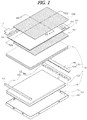
- FIG. 1 is an exploded perspective view of an LCD device according to a embodiment of the present invention.
- an LCD device includes a liquid crystal panel 110, a backlight unit 120, a main frame 130, and a bottom frame 150.
- the liquid crystal panel 110 includes first and second substrates 112 and 114 facing each other and a liquid crystal layer (not shown) therebetween.
- array elements for example, a gate line (not shown), a data line (not shown), a thin film transistor (not shown), and a pixel electrode (not shown), are formed on the first substrate 112.
- the gate and data lines cross each other to define a pixel region, and the thin film transistor is formed at a crossing point of the gate and data lines.
- the pixel electrode is disposed in the pixel region and is connected to the thin film transistor.
- a black matrix (not shown) corresponding to the gate line, the data line, and the thin film transistor to block light and a color filter layer (not shown) having red, green and blue colors are formed on the second substrate 114.
- a common electrode (not shown) is also formed on the second substrate 114 to generate an electric field with the pixel electrode on the first substrate 112.
- first and second polarizing plates 119a and 119b for selectively transmitting light are positioned on outer sides of the first and second substrates 112 and 114, respectively.
- the liquid crystal panel 110 is connected to a printed circuit board (PCB) 117 through a connection member 116, such as a flexible circuit board or a tape carrier package (TCP), and the printed circuit board 117 extends along a side surface of the main frame 130 or a rear surface of the bottom frame 150.
- PCB printed circuit board
- connection member 116 such as a flexible circuit board or a tape carrier package (TCP)
- TCP tape carrier package
- the backlight unit 120 provides light to the liquid crystal panel 110 and is disposed at a rear side of the liquid crystal panel 110.
- the backlight unit 110 includes a light emitting diode (LED) assembly 129 as a light source, a reflective sheet 125 of white or silver color, a light guide plate 123 on the reflective sheet 125 and an optical sheet 121 on or over the light guide plate 123.
- LED light emitting diode
- the LED assembly 129 is positioned at one side of the light guide plate 123 and includes at least one LED 129a and a printed circuit board (PCB) 129b where the LED 129a is disposed.
- PCB printed circuit board
- a direction of the light from the LEDs 129a is substantially parallel to a surface of the PCB 129b. This may be referred to as a side view type LED assembly.
- the LEDs 129a emit red, green and blue color light.
- the LEDs 129a are simultaneously turned on and off such that white light can be provided from the LEDs 129a by color mixture.
- an LED including a blue LED chip and a yellow fluorescent substance e.g., cesium-doped yttrium-aluminum-garnet (YAG:Ce), may be used.
- YAG:Ce cesium-doped yttrium-aluminum-garnet
- the blue light from the blue LED chip is mixed with the yellow light from the yellow fluorescent substance such that the white light is provided.
- the light emitted from the LED 129a is incident to the light guide plate 123 and refracted or reflected to be dispersed onto a wide region of the light guide plate 123.
- the light is processed into a planar light source and provided onto the liquid crystal panel 110.
- the light guide plate 123 is formed of a transparent material and has a flat surface.
- the light guide plate 123 may be formed of an acryl-based plastic material, e.g., polymethylmethacrylate (PMMA), or a polycarbonate-based material.
- PMMA polymethylmethacrylate
- the light guide plate 123 may include patterns on a rear side surface.
- the pattern on the rear side surface of the light guide plate 123 is an elliptical pattern, a polygonal pattern, or a hologram pattern.
- the reflective sheet 125 is disposed at a rear side of the light guide plate 123. The light passing through a rear side surface of the light guide plate 123 is reflected on the reflective sheet 125 such that light brightness provided into the liquid crystal panel 110 is improved.
- the optical sheet 121 includes a plurality of sheets, e.g., a diffusion sheet and at least one light-concentration sheet.
- the light dispersed through the light guide plate 123 is diffused and/or/ concentrated by the optical sheet 121 such that a uniform planar light source can be projected onto the liquid crystal panel 110.
- the diffusion sheet is disposed directly over the light guide plate 123 to diffuse the light from the light guide plate 123.
- the light is directed by the diffusion sheet toward the light-concentration sheet.
- the diffused light from the diffusion sheet is concentrated toward the liquid crystal panel 110 by the light-concentration sheet. Most of the light from the light-concentration sheet is substantially perpendicular to the liquid crystal panel 110.
- the optical sheet 121 may be a multi-functional optical sheet having both diffusing and light-concentration functions.
- the optical sheet 121 may have a laminated structure including the diffusion sheet and the light-concentration sheet.
- the multi-functional optical sheet may include a base substrate of a transparent material, a diffusion layer, which is disposed on the base layer, for light diffusion, and a light-concentration layer, which is disposed on the diffusion layer, for light concentration.
- the liquid crystal panel 110 and the backlight unit 120 are combined with the main frame 130 and the bottom frame 150 for assembly.
- the liquid crystal panel 110 and the backlight unit 120 are disposed on and over the bottom frame 150.
- the bottom frame 150 includes a horizontal surface 151 and a side surface 153 upwardly protruding from edges of the horizontal surface 151.
- the side surface 153 vertically protrudes.
- the rear side of the backlight unit 120 is covered by the horizontal surface 151 of the bottom frame 150.
- the main frame 130 surrounds side surfaces of the backlight unit 120.
- the liquid crystal panel 110 is attached and fixed to the main frame 130.
- the main frame 130 includes a first guide portion 130a and a second guide portion 130b facing and opposite to the first guide portion 130a.
- the LED assembly 129 is disposed in the first guide portion 130a.
- edges of the liquid crystal panel 110 are defined as first to fourth edges
- the LED assembly 129 corresponds to the first edge
- the second edge faces opposite to the first edge.
- the third and fourth edges are perpendicular to the first and second edges and face each other.
- the first and second guide portions 130a and 130b are separated from each other and correspond to the first and second edges, respectively.
- the first and second guide portions 130a and 130b each has a bar shape.
- the backlight unit 120 is disposed between the first and second guide portions 130a and 130b, and two opposite side surfaces of the backlight unit 120 are covered by the first and second guide portions 130a and 130b.
- the liquid crystal panel 110 is attached on and fixed to the first and second guide portions 130a and 130b.
- a narrow bezel structure may minimize the non-display area of the LCD device.
- the bottom edge surfaces of the liquid crystal panel 110 in the third and fourth edges are fixed to the side surface 153 of the bottom frame 150 using an adhesive such as glue, as described further with respect to FIG. 3B . Accordingly, the liquid crystal panel 110 is securely assembled with the bottom frame 150 without a main frame along the third and fourth edges.
- the main frame 130 may be referred to as a guide panel, a main support, or a mold frame
- the bottom frame 150 may be referred to as a cover bottom, a bottom cover, or a lower cover.
- the LCD device of the present invention does not require a top frame covering front edges of the liquid crystal panel 110, which reduces the thickness and weight of the LCD device and simplifies the assembly process. In addition, the production costs of the LCD device are reduced.
- the display area of the LCD device is increased and the bezel (which is a non-display area of the LCD device) is decreased by eliminating the top frame.
- the LCD device is a narrow bezel LCD device.
- the main frame 130 includes separated first and second guide portions 130a and 130b corresponding to the first and second edges of the liquid crystal panel 110 without portions corresponding to the third and fourth edges of the liquid crystal panel 110. As a result, the bezel of the LCD device is further narrowed.
- the LCD device is securely assembled.
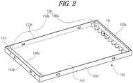
- FIG. 2 is a schematic perspective view of a main frame with a bottom frame.
- the bottom frame 150 includes the horizontal surface 151 and first to fourth side surfaces 153a to 153d vertically protruding form the horizontal surface 151.
- the first to fourth side surfaces 153a to 153d of the bottom frame 150 correspond to the first to fourth edges of the liquid crystal panel 110, respectively.
- the LED assembly 129 (of FIG. 1 ) is positioned to correspond to the first side surface 153a and the first edge of the liquid crystal panel 110.
- the first guide portion 130a of the main frame 130 is positioned on an inner side of the first side surface 153a
- the second guide portion 130b of the main frame is positioned on an inner side of the second side surface 153b.
- the first guide portion 130a has a length corresponding to a length of the first side surface 153a of the bottom frame 150 and includes an LED guide groove 131 for the LED 129a (of FIG. 1 ). Each LED 129a is inserted into each LED guide groove 131 such that three sides of the LED 129a are surrounded by the first guide portion 130a.
- the LED assembly 129 is attached on and fixed to the first guide portion 130a.
- the LED 129 is arranged and mounted on a surface of the PCB 129b (of FIG. 1 ) and is inserted into the LED groove 131 of the first guide portion 130a.
- the surface of the PCB 129b, where the LED 129 is arranged, is attached on and fixed to an upper surface of the first guide portion 130a.
- the LED assembly 129 has a fixed position in the LCD device by the first guide portion 130a.
- the second guide portion 130b has a length corresponding to a length of the second side surface 153b of the bottom frame 150, and a protrusion 133, which vertically protrudes from an upper surface of the second guide portion 130b, is positioned at both ends of the second guide portion 130b.
- the liquid crystal panel 110 is disposed on and supported by the protrusion 133.
- the protrusion 133 has substantially the same thickness as the PCB 129b of the LED assembly 129.
- the LED assembly 129 is attached to the first guide portion 130a by attaching the surface of the PCB 129b, where the LED 129a is arranged, to the upper surface of the first guide portion 130a, and the first edge of the liquid crystal panel 110 is attached to an opposite surface of the PCB 129b and supported by the LED assembly 129.
- the second edge of the liquid crystal panel 110 is attached to and supported by the protrusion 133 of the second guide portion 130b.
- the opposite surface (i.e., an upper surface) of the PCB 129b and the protrusion 133 have substantially the same height from the horizontal surface 151 of the bottom frame 150.
- first to fourth side surfaces 153a to 153d of the bottom frame 150 have substantially the same height from the horizontal surface 151 of the bottom frame 150 as the protrusion 133 and the PCB 129b.
- the liquid crystal panel 110 is securely attached and fixed to the PCB 129b and the protrusion 133 without an inclination or a gap.
- the opposite surface of the PCB 129b and the protrusion 133 form one horizontal plane.
- the first and second guide portions 130a and 130b which are separated from each other and respectively positioned at the first and second side surfaces 153a and 153b of the bottom frame 150, form the main frame 130 without portions at the third and fourth side surfaces 153c and 153c of the bottom frame 150. Accordingly, the non-display region at the third and fourth edges of the liquid crystal panel is minimized to provide a narrow bezel LCD device.
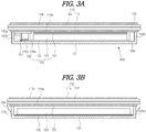
- FIGs. 3A and 3B are cross-sectional views along the lines III-III and III'-III' in FIG. 1 , respectively, whereby fig.3B corresponds to a sectional view of a not claimed first comparative example.
- the reflective sheet 125, the light guide plate 123, the LED assembly 129, which includes the LED 129a and the PCB 129b and is positioned at one side of the light guide plate 123, and the optical sheet 121 on the light guide plate 123 constitute the backlight unit 120.
- the liquid crystal panel 110 which includes the first and second substrates 112 and 114 and the liquid crystal layer (not shown) therebetween, is disposed over the backlight unit 120.
- the first and second polarizing plates 119a and 119b for selectively transmitting light are positioned on respective outer sides of the first and second substrates 112 and 114.
- the sides of the backlight unit 120 and the liquid crystal panel 110 are surrounded by the main frame 130, which includes the first and second guide portions 130a and 130b, and the bottom frame 150, which covers a rear side of the backlight unit 120 and is attached to the main frame 130.
- the LED 129a of the LED assembly 129 is inserted into the guide groove 131 formed in the first guide portion 130a of the main frame 130 such that the light from the LED 129a is incident toward the light guide plate 123.
- the PCB 129b is attached and fixed to the upper surface of the first guide portion 130a using an adhesive material such as double-faced tape.
- the liquid crystal panel 110 is attached to and supported by the PCB 129b, the protrusion 133 of the second guide portion 130b, and an upper surface of each of the first to fourth side surfaces 153a to 153d.
- the other two opposite sides of the backlight unit 120 are surrounded by the third and fourth side surfaces 153c and 153d of the bottom frame 150 without the main frame 130.
- the first side of the light guide plate 123 faces the LED 129a or the first guide portion 130a of the main frame 130, and the second side of the light guide plate 123 faces the second guide portion 130b of the main frame 130.
- the third and fourth sides of the light guide plate 123 face the third and fourth side surfaces 153c and 153d of the bottom frame 150, respectively.
- the liquid crystal panel 110 which is attached and fixed to the PCB 129b, the protrusion 133 of the second guide portion 130b, and the upper surface of each of the first to fourth side surfaces 153a to 153d, has a size larger than the bottom frame 150 such that edges of the liquid crystal panel 110 protrude beyond the bottom frame 150. Namely, the edges of the liquid crystal panel 110 protrude beyond the first to fourth side surfaces 153a to 153d.
- the rear edges of the liquid crystal panel 110 and an outer side of the side surfaces of the bottom frame 150 are attached by an adhesive 200 such as glue.
- the adhesive 200 may be formed at the third and fourth side surfaces 153c and 153d but not at the first and second side surfaces 153a and 153b because there is no main frame 130 in the third and fourth side surfaces 153c and 153d.
- the assembly of the LCD device is secured and the bezel of the LCD device is decreased.
- the positioning and/or coverage of the adhesive 200 in the third and fourth edges of the liquid crystal panel 110 are explained with respect to a second comparative example and an embodiments.
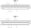
- FIG. 4 is a cross-sectional view along the line III'-III' in FIG. 1 of an LCD device according to a second comparative example.
- the reflective sheet 125, the light guide plate 123, the LED assembly 129, which includes the LED 129a and the PCB 129b and is positioned at one side of the light guide plate 123, and the optical sheet 121 on the light guide plate 123 constitute the backlight unit 120.
- the liquid crystal panel 110 which includes the first and second substrates 112 and 114 and the liquid crystal layer (not shown) therebetween, is disposed over the backlight unit 120.
- the first and second polarizing plates 119a and 119b for selectively transmitting light are positioned on outer sides of the first and second substrates 112 and 114.
- the sides of the backlight unit 120 and the liquid crystal panel 110 are surrounded by the main frame 130 (of FIG. 2 ), which includes the first and second guide portions 130a and 130b, and the bottom frame 150, which covers a rear side of the backlight unit 120 and is attached to the main frame 130.
- the liquid crystal panel 110 has a size larger than the bottom frame 150 such that edges of the liquid crystal panel 110 protrude beyond the bottom frame 150.
- the protruding edges of the liquid crystal panel 110 and an outer side of the third and fourth side surfaces 153c and 153d of the bottom frame 150 are attached with an adhesive 200 such as glue. Namely, the protruding edges liquid crystal panel 110 are attached and fixed to the third and fourth side surfaces 153c and 153d of the bottom frame 150 by the adhesive 200.
- the adhesive 200 covers sides of the liquid crystal panel 110.
- the adhesive 200 is formed to cover the side surface of the first and second substrates 112 and 114 of the liquid crystal panel 110, the exposed rear edge of the first substrate 112, the exposed rear edge of the first polarizing plate 119a, the side surface of the first polarizing plate 119a, and the outer side of the third and fourth side surfaces 153c and 153d of the bottom frame 150.
- the adhesive 200 has a black color and covers the side surfaces of the liquid crystal panel 110 such that light leakage from the side surfaces of the liquid crystal panel 110 is prevented or reduced due to the adhesive 200.
- the adhesive 200 is formed of a material that is highly light absorbing.
- the adhesion of the adhesive 200 is improved to more securely attach the liquid crystal panel 110 to the bottom frame 150.
- the thickness of the adhesive 200 at the side surfaces of the liquid crystal panel 110 is less than about 0.1mm such that the resulting increase in the bezel of the LCD device is minimized without light leakage (and while maintaining secure assembly).
- FIG. 5 is a cross-sectional view along the line III'-III' in FIG. 1 of an LCD device according to an embodiment of the present invention.
- the reflective sheet 125, the light guide plate 123, the LED assembly 129, which includes the LED 129a and the PCB 129b and is positioned at one side of the light guide plate 123, and the optical sheet 121 on the light guide plate 123 constitute the backlight unit 120.
- the liquid crystal panel 110 which includes the first and second substrates 112 and 114 and the liquid crystal layer (not shown) therebetween, is disposed over the backlight unit 120.
- the first and second polarizing plates 119a and 119b for selectively transmitting light are positioned on outer sides of the first and second substrates 112 and 114.
- the sides of the backlight unit 120 and the liquid crystal panel 110 are surrounded by the main frame 130 (of FIG. 2 ), which includes the first and second guide portions 130a and 130b, and the bottom frame 150, which covers a rear side of the backlight unit 120 and is attached to the main frame 130.
- the liquid crystal panel 110 has a size larger than the bottom frame 150 such that edges of the liquid crystal panel 110 protrude beyond the bottom frame 150.
- the protruding edges of the liquid crystal panel 110 and an outer side of the third and fourth side surfaces 153c and 153d of the bottom frame 150 are attached with an adhesive 200 such as glue. Namely, the protruding edges liquid crystal panel 110 are attached and fixed to the third and fourth side surfaces 153c and 153d of the bottom frame 150 by the adhesive 200.
- the second polarizing plate 119b at an outer side of the second substrate 114 of the liquid crystal panel 110 has a size larger than the liquid crystal panel 110. Namely, a rear edge of the second polarizing plate 119b protrudes beyond the liquid crystal panel 110.
- the sides of the second polarizing plate 119b corresponding to the third and fourth side surfaces 153c and 153d of the bottom frame 150 protrude beyond the liquid crystal panel 110, while the sides of the second polarizing plate 119b corresponding to the first and second side surfaces 153a and 153b of the bottom frame 150 may not protrude beyond the liquid crystal panel 110.
- ends of the second polarizing plate 119b corresponding to the first and second side surfaces 153a and 153b of the bottom frame 150 may be positioned inside the area of the liquid crystal panel 110.
- the adhesive 200 covers from the rear edge of the second polarizing plate 119b to the outer side of the third and fourth side surfaces 153c and 153d of the bottom frame 150.
- the adhesive 200 is formed to cover the rear edge of the second polarizing plate 119b, the side surface of the first and second substrates 112 and 114 of the liquid crystal panel 110, the exposed rear edge of the first substrate 112, the exposed rear edge of the first polarizing plate 119a, the side surface of the first polarizing plate 119a, and the outer side of the third and fourth side surfaces 153c and 153d of the bottom frame 150.
- the adhesive 200 has a black color and covers the side surface of the liquid crystal panel 110 such that light leakage from the side surface of the liquid crystal panel 110 is prevented or reduced due to the adhesive 200.
- the liquid crystal panel 110 is more securely attached to the bottom frame 150.
- the exposed edge of the second polarizing plate 119b serves as a dam in the process of coating a liquid phase material for the adhesive 200, the process efficiency for applying the adhesive 200 is improved.
- the second polarizing plate 119b has the larger size than the liquid crystal panel 110, the end of the second polarizing plate 119b is not positioned in the display area of the liquid crystal panel 110. Namely, the top frame covering front edges of the liquid crystal panel 110 and the front edges of the second polarizing plate 119b is unnecessary. As a result, the LCD device is a clear borderless type LCD device without a border between the image display screen and the frame.
- the LCD device of the present invention does not require the top frame, a thin and light-weight LCD device is provided and the assembly process is simplified. Production costs are also reduced.
- the display area is increased and the non-display area is decreased such that a narrow bezel LCD device is provided.
- the main frame 130 includes separated first and second guide portions 130a and 130b corresponding to the first and second edges of the liquid crystal panel 110 without portions corresponding to the third and fourth edges of the liquid crystal panel 110.
- the bezel of the LCD device is further narrowed.
- the third and fourth edges of the liquid crystal panel 110 without the portions of the main frame 130 are attached and fixed to the third and fourth side surfaces 153c and 153d of the bottom frame 150 by the adhesive 200 for secure assembly of the LCD device.
- the adhesive 200 has a black color and covers the side surface of the liquid crystal panel 110 such that light leakage from the side surface of the liquid crystal panel 110 is prevented or reduced due to the adhesive 200. Since the second polarizing plate 119b has a larger size than the liquid crystal panel 110, the process efficiency for applying the adhesive 200 is improved and a clear borderless type LCD device is provided.
Landscapes
- Physics & Mathematics (AREA)
- Nonlinear Science (AREA)
- General Physics & Mathematics (AREA)
- Optics & Photonics (AREA)
- Mathematical Physics (AREA)
- Chemical & Material Sciences (AREA)
- Crystallography & Structural Chemistry (AREA)
- Engineering & Computer Science (AREA)
- Microelectronics & Electronic Packaging (AREA)
- Manufacturing & Machinery (AREA)
- Geometry (AREA)
- Liquid Crystal (AREA)
Claims (8)
- Eine Flüssigkristall-Anzeigevorrichtung aufweisend:ein Flüssigkristall-Panel (110), das ein erstes und ein zweites Substrat (112, 114) und eine Flüssigkristall-Schicht zwischen dem ersten und dem zweiten Substrat (112, 114) aufweist;eine Hintergrundbeleuchtungseinheit (120) unter dem Flüssigkristall-Panel (110) und aufweisend eine Lichtleitplatte (123) und eine Lichtemittierende-Diode (LED)-Anordnung (129);einen Unterseitenrahmen (150), welcher eine horizontale Fläche (151) und eine erste, eine zweite, eine dritte und eine vierte Seitenfläche (153a, 153b, 153c, 153d) aufweist, wobei die erste Seitenfläche (153a) mit einem ersten Rand des Flüssigkristall-Panels (110) korrespondiert und gegenüber der zweiten Seitenfläche (153b) angeordnet ist, wobei das Flüssigkristall-Panel (110) eine Größe hat, die größer ist als der Unterseitenrahmen (150), sodass alle vier Seiten des Flüssigkristall-Panels (110) über die erste bis vierte Seitenfläche (153c, 153d) des Unterseitenrahmen (150) vorstehen;einen Hauptrahmen (130), welcher einen ersten Führungsabschnitt (130a) aufweist, der mit dem ersten Rand korrespondiert, und einen zweiten Führungsabschnitt (130b), der mit einem dem ersten Rand gegenüberliegenden zweiten Rand des Flüssigkristall-Panels (110) korrespondiert, wobei die Lichtleitplatte (123) und die LED-Anordnung (129) von dem ersten und dem zweiten Führungsabschnitt (130a, 130b) geführt werden, wobei der erste und der zweite Führungsabschnitt (130a, 130b) den Hauptrahmen (130) bilden, ohne Abschnitte an der dritten und vierten Seitenfläche (153c, 153d) des Unterseitenrahmens (150),wobei der erste Führungsabschnitt (130a) des Hauptrahmens (130) an einer Innenseite der ersten Seitenfläche (153a) angeordnet ist und der zweite Führungsabschnitt (130b) des Hauptrahmens (130) an einer Innenseite der zweiten Seitenfläche (153b) des Unterseitenrahmens (150) angeordnet ist;eine erste Polarisationsplatte (119a) an einer Außenseite des ersten Substrats (112), die zwischen dem Flüssigkristall-Panel (110) und der Hintergrundbeleuchtungseinheit (120) angeordnet ist;eine zweite Polarisationsplatte (119b) an einer Außenseite des zweiten Substrats (114), wobei zwei einander gegenüberliegende Seiten der zweiten Polarisationsplatte (119b), die mit der dritten und vierten Seitenfläche (153c, 153d) des Unterseitenrahmens (150) korrespondieren, über das Flüssigkristall-Panel (110) hinaus vorstehen, undeinen Klebstoff (200), der Seiten des Flüssigkristall-Panels (110) und eine Außenseite der dritten und vierten Seitenfläche (153c, 153d) bedeckt, wobei der Klebstoff (200) aus einem Material mit hohem Lichtabsorptionsgrad gebildet ist, wobei der Klebstoff (200) eine Rückseitenfläche der zwei einander gegenüberliegenden Seiten der zweiten Polarisationsplatte (119b), die Seiten des Flüssigkristall-Panels (110) und eine freiliegende Rückseitenfläche des Flüssigkristall-Panels (110), die mit der dritten und vierten Seitenfläche (153c, 153d) korrespondiert, sowie die dritte und vierte Seitenfläche (153c, 153d) des Unterseitenrahmens (150) bedeckt.
- Die Vorrichtung gemäß Anspruch 1, wobei die Seiten der zweiten Polarisationsplatte (119b), die mit der ersten und der zweiten Seitenfläche (153a, 153b) des Unterseitenrahmens (150) korrespondieren, nicht über das Flüssigkristall-Panel (110) hinaus vorstehen.
- Die Vorrichtung gemäß Anspruch 2,
wobei der Klebstoff (200) an den Seiten des Flüssigkristall-Panels (110) eine Dicke von weniger als 0,1 mm hat. - Die Vorrichtung gemäß irgendeinem der Ansprüche 1 bis 3,
wobei die LED-Anordnung (129) mit dem ersten Rand des Flüssigkristall-Panels (110) korrespondiert und eine Leiterplatte (PCB) (129b) und eine auf der Leiterplatte (129b) angeordnete LED (129a) aufweist, und wobei der erste Führungsabschnitt (130a) eine Führungsnut (131) aufweist, und die LED (129a) in die Führungsnut (131) eingeführt ist. - Die Vorrichtung gemäß Anspruch 4, ferner aufweisend ein vorstehendes Teil (133) an einer oberen Fläche des zweiten Führungsabschnitts (130b), wobei das vorstehende Teil (133) an einem Ende des zweiten Führungsabschnitts (130b) angeordnet ist, wobei die Leiterplatte (129b) an einer oberen Fläche des ersten Führungsabschnitts (130a) befestigt ist und von der horizontalen Fläche (151) eine im Wesentlichen gleiche Höhe hat wie das vorstehende Teil (133) von der horizontalen Fläche (151) hat.
- Die Vorrichtung gemäß Anspruch 5, wobei das Flüssigkristall-Panel (110) an der Leiterplatte (129b) und dem vorstehenden Teil (133) befestigt ist.
- Die Vorrichtung gemäß Anspruch 6,
wobei die erste, zweite, dritte und vierte Seitenfläche (153a, 153b, 153c, 153d) von der horizontalen Fläche (151) im Wesentlichen die gleiche Höhe haben wie das vorstehende Teil (133) von der horizontalen Fläche (151) hat. - Die Vorrichtung gemäß irgendeinem der Ansprüche 4 bis 7,
wobei die Hintergrundbeleuchtungseinheit (120) ferner aufweist:eine reflektierende Folie (125) an der horizontalen Fläche (151) und unter der Lichtleitplatte (123); undeine optische Folie (121) auf der Lichtleitplatte (123),wobei die LED-Anordnung (129) an einer ersten Seitenfläche der Lichtleitplatte (123) angeordnet ist.
Applications Claiming Priority (1)
| Application Number | Priority Date | Filing Date | Title |
|---|---|---|---|
| KR1020140023470A KR101541352B1 (ko) | 2014-02-27 | 2014-02-27 | 액정표시장치 |
Publications (2)
| Publication Number | Publication Date |
|---|---|
| EP2913706A1 EP2913706A1 (de) | 2015-09-02 |
| EP2913706B1 true EP2913706B1 (de) | 2018-03-14 |
Family
ID=52354851
Family Applications (1)
| Application Number | Title | Priority Date | Filing Date |
|---|---|---|---|
| EP15151878.4A Active EP2913706B1 (de) | 2014-02-27 | 2015-01-21 | Flüssigkristallanzeigevorrichtung |
Country Status (4)
| Country | Link |
|---|---|
| US (2) | US9395568B2 (de) |
| EP (1) | EP2913706B1 (de) |
| KR (1) | KR101541352B1 (de) |
| CN (2) | CN108333822B (de) |
Families Citing this family (38)
| Publication number | Priority date | Publication date | Assignee | Title |
|---|---|---|---|---|
| CN104360528B (zh) * | 2014-11-18 | 2017-06-06 | 深圳市华星光电技术有限公司 | 一种显示模组 |
| KR20160095291A (ko) * | 2015-02-02 | 2016-08-11 | 삼성디스플레이 주식회사 | 백라이트 유닛 및 이를 포함하는 표시 장치 |
| KR102359607B1 (ko) * | 2015-09-22 | 2022-02-08 | 삼성디스플레이 주식회사 | 표시 장치 |
| CN105242451A (zh) * | 2015-09-30 | 2016-01-13 | 深圳天珑无线科技有限公司 | 一种窄边框的显示装置及其制造方法 |
| KR102497471B1 (ko) * | 2015-10-30 | 2023-02-07 | 엘지디스플레이 주식회사 | 점착 레진을 포함하는 액정표시장치 및 이의 제조 방법 |
| KR102430070B1 (ko) * | 2015-10-30 | 2022-08-04 | 엘지디스플레이 주식회사 | 점착 레진을 포함하는 액정표시장치 및 이의 제조 방법 |
| CN105301840A (zh) * | 2015-11-18 | 2016-02-03 | 武汉华星光电技术有限公司 | 背光模组及液晶显示装置 |
| US10180534B2 (en) * | 2015-12-30 | 2019-01-15 | Lg Display Co., Ltd. | Borderless display device including display module |
| CN105607328A (zh) * | 2016-03-31 | 2016-05-25 | 京东方(河北)移动显示技术有限公司 | 一种显示装置及其制备方法 |
| JP2017198854A (ja) * | 2016-04-27 | 2017-11-02 | 株式会社ジャパンディスプレイ | 照明装置及び液晶表示装置 |
| JP2018004727A (ja) * | 2016-06-28 | 2018-01-11 | 株式会社ジャパンディスプレイ | 表示装置 |
| JP2018004728A (ja) * | 2016-06-28 | 2018-01-11 | 株式会社ジャパンディスプレイ | 表示装置および接着方法 |
| JP2018005074A (ja) | 2016-07-06 | 2018-01-11 | 株式会社ジャパンディスプレイ | 表示装置 |
| JP2018072515A (ja) | 2016-10-27 | 2018-05-10 | 株式会社ジャパンディスプレイ | 表示装置 |
| KR102545158B1 (ko) * | 2016-10-31 | 2023-06-20 | 엘지디스플레이 주식회사 | 디스플레이 장치 |
| CN106444154A (zh) * | 2016-11-16 | 2017-02-22 | 武汉华星光电技术有限公司 | 背光模组及液晶显示装置 |
| CN108089365A (zh) * | 2016-11-22 | 2018-05-29 | 群创光电股份有限公司 | 显示装置 |
| KR101846822B1 (ko) | 2016-11-30 | 2018-04-17 | (주)토비스 | 내로우 베젤을 갖는 액정표시장치 |
| CN106842695A (zh) * | 2016-12-19 | 2017-06-13 | 武汉华星光电技术有限公司 | 一种胶框、背光模组及液晶显示器 |
| JP6876553B2 (ja) | 2017-07-11 | 2021-05-26 | 株式会社ジャパンディスプレイ | 表示装置 |
| CN107238964B (zh) * | 2017-08-02 | 2020-05-05 | 深圳市华星光电技术有限公司 | 一种无边框液晶面板及其制作方法以及液晶模组 |
| US10288968B2 (en) | 2017-09-11 | 2019-05-14 | Visteon Global Technologies, Inc. | Electronic display with multiple polarizer layers |
| KR101846825B1 (ko) | 2017-09-25 | 2018-05-31 | (주)토비스 | 내로우 베젤을 갖는 액정표시장치 |
| JP2019082523A (ja) | 2017-10-30 | 2019-05-30 | 株式会社ジャパンディスプレイ | 液晶表示装置 |
| CN107966845A (zh) * | 2018-01-18 | 2018-04-27 | 广东欧珀移动通信有限公司 | 显示屏及电子设备 |
| CN108169946A (zh) * | 2018-01-18 | 2018-06-15 | 广东欧珀移动通信有限公司 | 显示屏组件及电子设备 |
| CN110161733A (zh) * | 2018-02-14 | 2019-08-23 | 群创光电股份有限公司 | 显示设备及其制造方法 |
| CN108924300A (zh) * | 2018-07-03 | 2018-11-30 | 京东方科技集团股份有限公司 | 背光模组及显示装置 |
| CN109188785A (zh) * | 2018-09-25 | 2019-01-11 | 南京中电熊猫平板显示科技有限公司 | 一种液晶模组及其制造方法 |
| CN111352262A (zh) * | 2018-12-21 | 2020-06-30 | 群创光电股份有限公司 | 电子装置 |
| US11324128B2 (en) | 2019-02-07 | 2022-05-03 | Microsoft Technology Licensing, Llc | Display device and mounting bracket for bezel |
| CN111722424A (zh) | 2019-03-19 | 2020-09-29 | 鸿富锦精密工业(深圳)有限公司 | 显示设备及其显示模组 |
| KR102187028B1 (ko) | 2019-07-24 | 2020-12-04 | 주식회사 토비스 | 곡면 커버렌즈와 액정디스플레이의 합착방법 |
| KR102187026B1 (ko) | 2019-07-24 | 2020-12-04 | 주식회사 토비스 | 굴곡마스크를 이용한 곡면 커버렌즈의 레진 도포 방법 |
| KR102187025B1 (ko) | 2019-07-24 | 2020-12-04 | 주식회사 토비스 | 디스플레이 제조용 굴곡마스크 |
| US11536996B2 (en) * | 2019-10-08 | 2022-12-27 | Innolux Corporation | Display device |
| KR102671717B1 (ko) | 2019-10-25 | 2024-06-04 | 삼성전자주식회사 | 디스플레이 장치 |
| KR102821517B1 (ko) * | 2019-12-31 | 2025-06-16 | 엘지디스플레이 주식회사 | 표시모듈 및 이를 구비한 타일링 표시장치 |
Family Cites Families (20)
| Publication number | Priority date | Publication date | Assignee | Title |
|---|---|---|---|---|
| KR20060019654A (ko) | 2004-08-28 | 2006-03-06 | 삼성전자주식회사 | 백라이트 어셈블리 및 이를 갖는 액정표시장치 |
| CN201083925Y (zh) | 2007-07-04 | 2008-07-09 | 群康科技(深圳)有限公司 | 背光模组与液晶显示装置 |
| JP4575486B2 (ja) * | 2007-10-24 | 2010-11-04 | セイコーインスツル株式会社 | 表示装置 |
| KR101306136B1 (ko) * | 2008-06-16 | 2013-09-09 | 엘지디스플레이 주식회사 | 액정표시장치 |
| KR101117638B1 (ko) | 2010-02-01 | 2012-03-06 | 삼성모바일디스플레이주식회사 | 평판표시장치 및 이를 이용한 모바일 기기 |
| JP5433465B2 (ja) * | 2010-03-16 | 2014-03-05 | 株式会社ジャパンディスプレイ | 表示装置 |
| TWI410719B (zh) | 2010-03-25 | 2013-10-01 | Au Optronics Corp | 具強化結構之面板顯示模組及其製造方法 |
| KR101327743B1 (ko) * | 2010-04-27 | 2013-11-11 | 엘지디스플레이 주식회사 | 디스플레이 장치 |
| TWI462067B (zh) * | 2010-04-27 | 2014-11-21 | Lg Display Co Ltd | 顯示設備 |
| KR20120117073A (ko) * | 2011-04-14 | 2012-10-24 | 장경원 | 물 절약형 변기의 형성, 제조 방법. |
| KR101383207B1 (ko) * | 2011-05-02 | 2014-04-10 | 엘지디스플레이 주식회사 | 디스플레이 장치 |
| TWI431366B (zh) * | 2011-07-08 | 2014-03-21 | Au Optronics Corp | 顯示模組及其製造方法 |
| EP2804046B1 (de) * | 2011-07-27 | 2016-10-19 | LG Display Co., Ltd. | Anzeigevorrichtung und Herstellungsverfahren dafür |
| KR101930298B1 (ko) | 2011-09-22 | 2018-12-18 | 엘지디스플레이 주식회사 | 입체 영상 표시 장치 |
| KR101942983B1 (ko) | 2011-12-23 | 2019-01-29 | 엘지디스플레이 주식회사 | 액정표시장치 |
| KR101436806B1 (ko) * | 2012-03-08 | 2014-09-03 | 엘지디스플레이 주식회사 | 디스플레이 장치 및 그의 제조 방법 |
| TW201341894A (zh) * | 2012-04-06 | 2013-10-16 | Au Optronics Corp | 顯示裝置及其組裝方法 |
| KR20140020157A (ko) | 2012-08-08 | 2014-02-18 | 삼성디스플레이 주식회사 | 액정 표시 장치 및 그 제법 |
| KR102076503B1 (ko) * | 2013-01-24 | 2020-02-13 | 엘지디스플레이 주식회사 | 디스플레이 패널 및 이를 포함하는 디스플레이 장치 |
| CN203241655U (zh) * | 2013-03-27 | 2013-10-16 | 北京京东方光电科技有限公司 | 一种显示装置 |
-
2014
- 2014-02-27 KR KR1020140023470A patent/KR101541352B1/ko active Active
- 2014-08-05 US US14/451,720 patent/US9395568B2/en active Active
-
2015
- 2015-01-21 EP EP15151878.4A patent/EP2913706B1/de active Active
- 2015-02-15 CN CN201810229832.9A patent/CN108333822B/zh active Active
- 2015-02-15 CN CN201510082696.1A patent/CN104880839B/zh active Active
-
2016
- 2016-06-22 US US15/189,727 patent/US9715135B2/en active Active
Non-Patent Citations (1)
| Title |
|---|
| None * |
Also Published As
| Publication number | Publication date |
|---|---|
| EP2913706A1 (de) | 2015-09-02 |
| KR101541352B1 (ko) | 2015-08-03 |
| CN104880839A (zh) | 2015-09-02 |
| US20150241731A1 (en) | 2015-08-27 |
| CN108333822B (zh) | 2021-01-22 |
| US20160306219A1 (en) | 2016-10-20 |
| US9395568B2 (en) | 2016-07-19 |
| CN104880839B (zh) | 2018-07-24 |
| CN108333822A (zh) | 2018-07-27 |
| US9715135B2 (en) | 2017-07-25 |
Similar Documents
| Publication | Publication Date | Title |
|---|---|---|
| EP2913706B1 (de) | Flüssigkristallanzeigevorrichtung | |
| KR102395088B1 (ko) | 백라이트 유닛 및 이를 포함하는 액정 표시 장치 | |
| EP2821842B1 (de) | Rückbeleuchtungseinheit und Flüssigkristallanzeige damit | |
| EP2696234B1 (de) | Hintergrundbeleuchtungsvorrichtung | |
| CN107357063A (zh) | 显示装置与包括该显示装置的拼接显示设备 | |
| TWI463222B (zh) | 背光單元及包含背光單元之液晶顯示器 | |
| KR102033481B1 (ko) | 액정표시장치 | |
| KR102460231B1 (ko) | 백라이트 유닛 및 이를 포함하는 액정 표시 장치 | |
| WO2011152133A1 (ja) | 照明装置、表示装置及びテレビ受信装置 | |
| US9304345B2 (en) | Liquid crystal display device | |
| WO2012128193A1 (ja) | 照明装置及び表示装置 | |
| KR20140022154A (ko) | 액정표시장치 | |
| KR20090128693A (ko) | 액정표시장치 | |
| KR101961721B1 (ko) | 액정표시장치 | |
| KR20160147110A (ko) | 표시 장치 | |
| KR20120116290A (ko) | 액정표시장치 | |
| US20170315290A1 (en) | Display apparatus | |
| KR102831847B1 (ko) | 표시 장치 | |
| KR102002458B1 (ko) | 액정표시장치 | |
| KR20120075115A (ko) | 도광판, 이를 구비한 백라이트 유닛 및 이들을 포함하는 액정표시장치 | |
| KR102565594B1 (ko) | 바텀커버 및 이를 포함하는 표시장치 | |
| KR20170079244A (ko) | 액정 표시 장치 | |
| KR20150068628A (ko) | 액정표시장치 | |
| KR101832309B1 (ko) | 디스플레이 장치 | |
| KR20110134067A (ko) | 액정표시장치 및 그 조립방법 |
Legal Events
| Date | Code | Title | Description |
|---|---|---|---|
| PUAI | Public reference made under article 153(3) epc to a published international application that has entered the european phase |
Free format text: ORIGINAL CODE: 0009012 |
|
| 17P | Request for examination filed |
Effective date: 20150121 |
|
| AK | Designated contracting states |
Kind code of ref document: A1 Designated state(s): AL AT BE BG CH CY CZ DE DK EE ES FI FR GB GR HR HU IE IS IT LI LT LU LV MC MK MT NL NO PL PT RO RS SE SI SK SM TR |
|
| AX | Request for extension of the european patent |
Extension state: BA ME |
|
| RBV | Designated contracting states (corrected) |
Designated state(s): AL AT BE BG CH CY CZ DE DK EE ES FI FR GB GR HR HU IE IS IT LI LT LU LV MC MK MT NL NO PL PT RO RS SE SI SK SM TR |
|
| GRAP | Despatch of communication of intention to grant a patent |
Free format text: ORIGINAL CODE: EPIDOSNIGR1 |
|
| STAA | Information on the status of an ep patent application or granted ep patent |
Free format text: STATUS: GRANT OF PATENT IS INTENDED |
|
| INTG | Intention to grant announced |
Effective date: 20170928 |
|
| RIN1 | Information on inventor provided before grant (corrected) |
Inventor name: LEE, KWANG-MIN Inventor name: KIM, MIN-WOO Inventor name: YANG, SEUNG-HOON Inventor name: JEONG, HAE-HYEON Inventor name: KIM, MI-RA Inventor name: KIM, WON-TAE |
|
| GRAS | Grant fee paid |
Free format text: ORIGINAL CODE: EPIDOSNIGR3 |
|
| GRAA | (expected) grant |
Free format text: ORIGINAL CODE: 0009210 |
|
| STAA | Information on the status of an ep patent application or granted ep patent |
Free format text: STATUS: THE PATENT HAS BEEN GRANTED |
|
| AK | Designated contracting states |
Kind code of ref document: B1 Designated state(s): AL AT BE BG CH CY CZ DE DK EE ES FI FR GB GR HR HU IE IS IT LI LT LU LV MC MK MT NL NO PL PT RO RS SE SI SK SM TR |
|
| REG | Reference to a national code |
Ref country code: GB Ref legal event code: FG4D |
|
| REG | Reference to a national code |
Ref country code: CH Ref legal event code: EP Ref country code: AT Ref legal event code: REF Ref document number: 979446 Country of ref document: AT Kind code of ref document: T Effective date: 20180315 |
|
| REG | Reference to a national code |
Ref country code: IE Ref legal event code: FG4D |
|
| REG | Reference to a national code |
Ref country code: DE Ref legal event code: R096 Ref document number: 602015008634 Country of ref document: DE |
|
| REG | Reference to a national code |
Ref country code: NL Ref legal event code: MP Effective date: 20180314 |
|
| REG | Reference to a national code |
Ref country code: LT Ref legal event code: MG4D |
|
| PG25 | Lapsed in a contracting state [announced via postgrant information from national office to epo] |
Ref country code: HR Free format text: LAPSE BECAUSE OF FAILURE TO SUBMIT A TRANSLATION OF THE DESCRIPTION OR TO PAY THE FEE WITHIN THE PRESCRIBED TIME-LIMIT Effective date: 20180314 Ref country code: LT Free format text: LAPSE BECAUSE OF FAILURE TO SUBMIT A TRANSLATION OF THE DESCRIPTION OR TO PAY THE FEE WITHIN THE PRESCRIBED TIME-LIMIT Effective date: 20180314 Ref country code: CY Free format text: LAPSE BECAUSE OF FAILURE TO SUBMIT A TRANSLATION OF THE DESCRIPTION OR TO PAY THE FEE WITHIN THE PRESCRIBED TIME-LIMIT Effective date: 20180314 Ref country code: NO Free format text: LAPSE BECAUSE OF FAILURE TO SUBMIT A TRANSLATION OF THE DESCRIPTION OR TO PAY THE FEE WITHIN THE PRESCRIBED TIME-LIMIT Effective date: 20180614 Ref country code: FI Free format text: LAPSE BECAUSE OF FAILURE TO SUBMIT A TRANSLATION OF THE DESCRIPTION OR TO PAY THE FEE WITHIN THE PRESCRIBED TIME-LIMIT Effective date: 20180314 |
|
| REG | Reference to a national code |
Ref country code: AT Ref legal event code: MK05 Ref document number: 979446 Country of ref document: AT Kind code of ref document: T Effective date: 20180314 |
|
| PG25 | Lapsed in a contracting state [announced via postgrant information from national office to epo] |
Ref country code: SE Free format text: LAPSE BECAUSE OF FAILURE TO SUBMIT A TRANSLATION OF THE DESCRIPTION OR TO PAY THE FEE WITHIN THE PRESCRIBED TIME-LIMIT Effective date: 20180314 Ref country code: LV Free format text: LAPSE BECAUSE OF FAILURE TO SUBMIT A TRANSLATION OF THE DESCRIPTION OR TO PAY THE FEE WITHIN THE PRESCRIBED TIME-LIMIT Effective date: 20180314 Ref country code: RS Free format text: LAPSE BECAUSE OF FAILURE TO SUBMIT A TRANSLATION OF THE DESCRIPTION OR TO PAY THE FEE WITHIN THE PRESCRIBED TIME-LIMIT Effective date: 20180314 Ref country code: GR Free format text: LAPSE BECAUSE OF FAILURE TO SUBMIT A TRANSLATION OF THE DESCRIPTION OR TO PAY THE FEE WITHIN THE PRESCRIBED TIME-LIMIT Effective date: 20180615 Ref country code: BG Free format text: LAPSE BECAUSE OF FAILURE TO SUBMIT A TRANSLATION OF THE DESCRIPTION OR TO PAY THE FEE WITHIN THE PRESCRIBED TIME-LIMIT Effective date: 20180614 |
|
| PG25 | Lapsed in a contracting state [announced via postgrant information from national office to epo] |
Ref country code: AL Free format text: LAPSE BECAUSE OF FAILURE TO SUBMIT A TRANSLATION OF THE DESCRIPTION OR TO PAY THE FEE WITHIN THE PRESCRIBED TIME-LIMIT Effective date: 20180314 Ref country code: ES Free format text: LAPSE BECAUSE OF FAILURE TO SUBMIT A TRANSLATION OF THE DESCRIPTION OR TO PAY THE FEE WITHIN THE PRESCRIBED TIME-LIMIT Effective date: 20180314 Ref country code: PL Free format text: LAPSE BECAUSE OF FAILURE TO SUBMIT A TRANSLATION OF THE DESCRIPTION OR TO PAY THE FEE WITHIN THE PRESCRIBED TIME-LIMIT Effective date: 20180314 Ref country code: EE Free format text: LAPSE BECAUSE OF FAILURE TO SUBMIT A TRANSLATION OF THE DESCRIPTION OR TO PAY THE FEE WITHIN THE PRESCRIBED TIME-LIMIT Effective date: 20180314 Ref country code: NL Free format text: LAPSE BECAUSE OF FAILURE TO SUBMIT A TRANSLATION OF THE DESCRIPTION OR TO PAY THE FEE WITHIN THE PRESCRIBED TIME-LIMIT Effective date: 20180314 Ref country code: RO Free format text: LAPSE BECAUSE OF FAILURE TO SUBMIT A TRANSLATION OF THE DESCRIPTION OR TO PAY THE FEE WITHIN THE PRESCRIBED TIME-LIMIT Effective date: 20180314 |
|
| PG25 | Lapsed in a contracting state [announced via postgrant information from national office to epo] |
Ref country code: SK Free format text: LAPSE BECAUSE OF FAILURE TO SUBMIT A TRANSLATION OF THE DESCRIPTION OR TO PAY THE FEE WITHIN THE PRESCRIBED TIME-LIMIT Effective date: 20180314 Ref country code: SM Free format text: LAPSE BECAUSE OF FAILURE TO SUBMIT A TRANSLATION OF THE DESCRIPTION OR TO PAY THE FEE WITHIN THE PRESCRIBED TIME-LIMIT Effective date: 20180314 Ref country code: CZ Free format text: LAPSE BECAUSE OF FAILURE TO SUBMIT A TRANSLATION OF THE DESCRIPTION OR TO PAY THE FEE WITHIN THE PRESCRIBED TIME-LIMIT Effective date: 20180314 Ref country code: AT Free format text: LAPSE BECAUSE OF FAILURE TO SUBMIT A TRANSLATION OF THE DESCRIPTION OR TO PAY THE FEE WITHIN THE PRESCRIBED TIME-LIMIT Effective date: 20180314 |
|
| REG | Reference to a national code |
Ref country code: DE Ref legal event code: R097 Ref document number: 602015008634 Country of ref document: DE |
|
| PG25 | Lapsed in a contracting state [announced via postgrant information from national office to epo] |
Ref country code: PT Free format text: LAPSE BECAUSE OF FAILURE TO SUBMIT A TRANSLATION OF THE DESCRIPTION OR TO PAY THE FEE WITHIN THE PRESCRIBED TIME-LIMIT Effective date: 20180716 |
|
| PLBE | No opposition filed within time limit |
Free format text: ORIGINAL CODE: 0009261 |
|
| STAA | Information on the status of an ep patent application or granted ep patent |
Free format text: STATUS: NO OPPOSITION FILED WITHIN TIME LIMIT |
|
| PG25 | Lapsed in a contracting state [announced via postgrant information from national office to epo] |
Ref country code: DK Free format text: LAPSE BECAUSE OF FAILURE TO SUBMIT A TRANSLATION OF THE DESCRIPTION OR TO PAY THE FEE WITHIN THE PRESCRIBED TIME-LIMIT Effective date: 20180314 |
|
| 26N | No opposition filed |
Effective date: 20181217 |
|
| PG25 | Lapsed in a contracting state [announced via postgrant information from national office to epo] |
Ref country code: IT Free format text: LAPSE BECAUSE OF FAILURE TO SUBMIT A TRANSLATION OF THE DESCRIPTION OR TO PAY THE FEE WITHIN THE PRESCRIBED TIME-LIMIT Effective date: 20180314 Ref country code: SI Free format text: LAPSE BECAUSE OF FAILURE TO SUBMIT A TRANSLATION OF THE DESCRIPTION OR TO PAY THE FEE WITHIN THE PRESCRIBED TIME-LIMIT Effective date: 20180314 |
|
| PG25 | Lapsed in a contracting state [announced via postgrant information from national office to epo] |
Ref country code: MC Free format text: LAPSE BECAUSE OF FAILURE TO SUBMIT A TRANSLATION OF THE DESCRIPTION OR TO PAY THE FEE WITHIN THE PRESCRIBED TIME-LIMIT Effective date: 20180314 |
|
| REG | Reference to a national code |
Ref country code: CH Ref legal event code: PL |
|
| PG25 | Lapsed in a contracting state [announced via postgrant information from national office to epo] |
Ref country code: LU Free format text: LAPSE BECAUSE OF NON-PAYMENT OF DUE FEES Effective date: 20190121 |
|
| REG | Reference to a national code |
Ref country code: BE Ref legal event code: MM Effective date: 20190131 |
|
| REG | Reference to a national code |
Ref country code: IE Ref legal event code: MM4A |
|
| PG25 | Lapsed in a contracting state [announced via postgrant information from national office to epo] |
Ref country code: BE Free format text: LAPSE BECAUSE OF NON-PAYMENT OF DUE FEES Effective date: 20190131 |
|
| PG25 | Lapsed in a contracting state [announced via postgrant information from national office to epo] |
Ref country code: CH Free format text: LAPSE BECAUSE OF NON-PAYMENT OF DUE FEES Effective date: 20190131 Ref country code: LI Free format text: LAPSE BECAUSE OF NON-PAYMENT OF DUE FEES Effective date: 20190131 |
|
| PG25 | Lapsed in a contracting state [announced via postgrant information from national office to epo] |
Ref country code: IE Free format text: LAPSE BECAUSE OF NON-PAYMENT OF DUE FEES Effective date: 20190121 |
|
| PG25 | Lapsed in a contracting state [announced via postgrant information from national office to epo] |
Ref country code: TR Free format text: LAPSE BECAUSE OF FAILURE TO SUBMIT A TRANSLATION OF THE DESCRIPTION OR TO PAY THE FEE WITHIN THE PRESCRIBED TIME-LIMIT Effective date: 20180314 |
|
| PG25 | Lapsed in a contracting state [announced via postgrant information from national office to epo] |
Ref country code: MT Free format text: LAPSE BECAUSE OF NON-PAYMENT OF DUE FEES Effective date: 20190121 |
|
| PG25 | Lapsed in a contracting state [announced via postgrant information from national office to epo] |
Ref country code: IS Free format text: LAPSE BECAUSE OF FAILURE TO SUBMIT A TRANSLATION OF THE DESCRIPTION OR TO PAY THE FEE WITHIN THE PRESCRIBED TIME-LIMIT Effective date: 20180714 |
|
| PG25 | Lapsed in a contracting state [announced via postgrant information from national office to epo] |
Ref country code: HU Free format text: LAPSE BECAUSE OF FAILURE TO SUBMIT A TRANSLATION OF THE DESCRIPTION OR TO PAY THE FEE WITHIN THE PRESCRIBED TIME-LIMIT; INVALID AB INITIO Effective date: 20150121 |
|
| PG25 | Lapsed in a contracting state [announced via postgrant information from national office to epo] |
Ref country code: MK Free format text: LAPSE BECAUSE OF FAILURE TO SUBMIT A TRANSLATION OF THE DESCRIPTION OR TO PAY THE FEE WITHIN THE PRESCRIBED TIME-LIMIT Effective date: 20180314 |
|
| PGFP | Annual fee paid to national office [announced via postgrant information from national office to epo] |
Ref country code: DE Payment date: 20241121 Year of fee payment: 11 |
|
| PGFP | Annual fee paid to national office [announced via postgrant information from national office to epo] |
Ref country code: GB Payment date: 20251120 Year of fee payment: 12 |
|
| PGFP | Annual fee paid to national office [announced via postgrant information from national office to epo] |
Ref country code: FR Payment date: 20251125 Year of fee payment: 12 |