EP2858129A2 - Lichtemittierendes Halbleiterbauelement und Herstellungsverfahren - Google Patents
Lichtemittierendes Halbleiterbauelement und Herstellungsverfahren Download PDFInfo
- Publication number
- EP2858129A2 EP2858129A2 EP20140177043 EP14177043A EP2858129A2 EP 2858129 A2 EP2858129 A2 EP 2858129A2 EP 20140177043 EP20140177043 EP 20140177043 EP 14177043 A EP14177043 A EP 14177043A EP 2858129 A2 EP2858129 A2 EP 2858129A2
- Authority
- EP
- European Patent Office
- Prior art keywords
- semiconductor layer
- layer
- sealing member
- light emitting
- emitting device
- Prior art date
- Legal status (The legal status is an assumption and is not a legal conclusion. Google has not performed a legal analysis and makes no representation as to the accuracy of the status listed.)
- Granted
Links
Images








Classifications
-
- H—ELECTRICITY
- H10—SEMICONDUCTOR DEVICES; ELECTRIC SOLID-STATE DEVICES NOT OTHERWISE PROVIDED FOR
- H10H—INORGANIC LIGHT-EMITTING SEMICONDUCTOR DEVICES HAVING POTENTIAL BARRIERS
- H10H20/00—Individual inorganic light-emitting semiconductor devices having potential barriers, e.g. light-emitting diodes [LED]
- H10H20/80—Constructional details
- H10H20/85—Packages
- H10H20/852—Encapsulations
- H10H20/853—Encapsulations characterised by their shape
-
- H—ELECTRICITY
- H10—SEMICONDUCTOR DEVICES; ELECTRIC SOLID-STATE DEVICES NOT OTHERWISE PROVIDED FOR
- H10H—INORGANIC LIGHT-EMITTING SEMICONDUCTOR DEVICES HAVING POTENTIAL BARRIERS
- H10H20/00—Individual inorganic light-emitting semiconductor devices having potential barriers, e.g. light-emitting diodes [LED]
- H10H20/80—Constructional details
- H10H20/85—Packages
- H10H20/851—Wavelength conversion means
-
- H—ELECTRICITY
- H10—SEMICONDUCTOR DEVICES; ELECTRIC SOLID-STATE DEVICES NOT OTHERWISE PROVIDED FOR
- H10H—INORGANIC LIGHT-EMITTING SEMICONDUCTOR DEVICES HAVING POTENTIAL BARRIERS
- H10H20/00—Individual inorganic light-emitting semiconductor devices having potential barriers, e.g. light-emitting diodes [LED]
- H10H20/01—Manufacture or treatment
- H10H20/011—Manufacture or treatment of bodies, e.g. forming semiconductor layers
- H10H20/018—Bonding of wafers
-
- H—ELECTRICITY
- H10—SEMICONDUCTOR DEVICES; ELECTRIC SOLID-STATE DEVICES NOT OTHERWISE PROVIDED FOR
- H10H—INORGANIC LIGHT-EMITTING SEMICONDUCTOR DEVICES HAVING POTENTIAL BARRIERS
- H10H20/00—Individual inorganic light-emitting semiconductor devices having potential barriers, e.g. light-emitting diodes [LED]
- H10H20/01—Manufacture or treatment
- H10H20/034—Manufacture or treatment of coatings
-
- H—ELECTRICITY
- H10—SEMICONDUCTOR DEVICES; ELECTRIC SOLID-STATE DEVICES NOT OTHERWISE PROVIDED FOR
- H10H—INORGANIC LIGHT-EMITTING SEMICONDUCTOR DEVICES HAVING POTENTIAL BARRIERS
- H10H20/00—Individual inorganic light-emitting semiconductor devices having potential barriers, e.g. light-emitting diodes [LED]
- H10H20/01—Manufacture or treatment
- H10H20/036—Manufacture or treatment of packages
- H10H20/0362—Manufacture or treatment of packages of encapsulations
-
- H—ELECTRICITY
- H10—SEMICONDUCTOR DEVICES; ELECTRIC SOLID-STATE DEVICES NOT OTHERWISE PROVIDED FOR
- H10H—INORGANIC LIGHT-EMITTING SEMICONDUCTOR DEVICES HAVING POTENTIAL BARRIERS
- H10H20/00—Individual inorganic light-emitting semiconductor devices having potential barriers, e.g. light-emitting diodes [LED]
- H10H20/80—Constructional details
- H10H20/84—Coatings, e.g. passivation layers or antireflective coatings
- H10H20/841—Reflective coatings, e.g. dielectric Bragg reflectors
-
- H—ELECTRICITY
- H10—SEMICONDUCTOR DEVICES; ELECTRIC SOLID-STATE DEVICES NOT OTHERWISE PROVIDED FOR
- H10H—INORGANIC LIGHT-EMITTING SEMICONDUCTOR DEVICES HAVING POTENTIAL BARRIERS
- H10H20/00—Individual inorganic light-emitting semiconductor devices having potential barriers, e.g. light-emitting diodes [LED]
- H10H20/80—Constructional details
- H10H20/85—Packages
- H10H20/851—Wavelength conversion means
- H10H20/8514—Wavelength conversion means characterised by their shape, e.g. plate or foil
-
- H—ELECTRICITY
- H10—SEMICONDUCTOR DEVICES; ELECTRIC SOLID-STATE DEVICES NOT OTHERWISE PROVIDED FOR
- H10H—INORGANIC LIGHT-EMITTING SEMICONDUCTOR DEVICES HAVING POTENTIAL BARRIERS
- H10H20/00—Individual inorganic light-emitting semiconductor devices having potential barriers, e.g. light-emitting diodes [LED]
- H10H20/80—Constructional details
- H10H20/85—Packages
- H10H20/855—Optical field-shaping means, e.g. lenses
- H10H20/856—Reflecting means
Definitions
- Embodiments described herein relate generally to a semiconductor light emitting device and a method for manufacturing the same.
- a method for manufacturing a semiconductor light emitting device in which a semiconductor layer is grown by crystal growth on a wafer; electrodes are formed on the semiconductor layer; sealing with a resin body is performed; subsequently, the wafer is removed; a fluorescer layer is formed on the exposed surface of the semiconductor layer; and dicing is performed. According to such a method, fine structural bodies that are formed on the wafer can be packaged as-is; and fine semiconductor light emitting devices can be efficiently manufactured.
- a semiconductor light emitting device includes a semiconductor layer, a sealing member configured to cover a lower surface of the semiconductor layer and a side surface of the semiconductor layer to protrude to be higher than an upper surface of the semiconductor layer at a side of the semiconductor layer, a fluorescer layer provided above the semiconductor layer and the sealing member, and an insulating film provided between the sealing member and the semiconductor layer and between the sealing member and the fluorescer layer.
- a corner of a protruding portion of the sealing member is rounded.
- a semiconductor light emitting device includes a semiconductor layer, an electrode connected to the semiconductor layer, a sealing member configured to cover a lower surface and a side surface of a structural body made of the semiconductor layer and the electrode, a fluorescer layer provided above the semiconductor layer and the sealing member, and an insulating film provided between the semiconductor layer and the sealing member and between the fluorescer layer and the sealing member.
- the sealing member includes the metal portion and the resin portion. An end portion of the metal portion extends onto an end portion of the electrode with the insulating film interposed.
- a method for manufacturing a semiconductor light emitting device includes growing a semiconductor layer on a substrate.
- the method includes dividing the semiconductor layer into a plurality of portions by selectively removing the semiconductor layer, and making a trench in a region of the substrate corresponding to a space between the plurality of portions.
- the method includes rounding a corner of the trench.
- the method includes forming an insulating film to cover the substrate, the semiconductor layer, and the corner.
- the method includes forming a sealing member on the insulating film.
- the method includes removing the substrate.
- the method includes forming a fluorescer layer to cover a surface that was opposing the substrate, the surface being formed of the semiconductor layer and the insulating film.
- FIG. 1A is a cross-sectional view showing a semiconductor light emitting device according to the embodiment; and FIG. 1B is a bottom view of FIG. 1A .
- FIG. 2A is a partially-enlarged cross-sectional view showing region A of FIG. 1A ; and FIG. 2B is a partially-enlarged cross-sectional view showing region B.
- FIG. 2B only a semiconductor layer 10, an n-side electrode 11n, a p-side electrode 11p, and an interconnect layer 13 are shown for easier viewing of the drawing. Further, the edge lines illustrating the configurations of these members are not shown.
- the configuration of the entire semiconductor light emitting device 1 is a rectangular parallelepiped.
- a semiconductor layer 10 is provided in the semiconductor light emitting device 1.
- the semiconductor layer 10 is formed of a compound semiconductor including, for example, gallium nitride (GaN) and is an LED (Light Emitting Diode) layer in which a p-type clad layer, an active layer, and an n-type clad layer are stacked in order from the lower layer side.
- GaN gallium nitride
- LED Light Emitting Diode
- the configuration of the semiconductor layer 10 is a rectangle, e.g., a square; and at the four corners of the rectangle, the p-type clad layer and the active layer are removed and the n-type clad layer is exposed. Also, a fine unevenness that has a period that is about the same as the wavelength of the light emitted by the semiconductor layer 10 is formed in an upper surface 10a of the semiconductor layer 10.
- the n-type clad layer, the active layer, and the p-type clad layer are portions of the semiconductor layer 10 but are not discriminated in the illustration of FIGS. 1A and 1B . This is similar for other drawings described below.
- n-side electrode 11n and a p-side electrode 11p are provided on the lower surface of the semiconductor layer 10.
- the n-side electrode 11n is connected to the n-type clad layer of the semiconductor layer 10; and the p-side electrode 11p is connected to the p-type clad layer of the semiconductor layer 10.
- an aluminum (Al) layer is provided on the semiconductor layer 10 side; and a gold (Au) layer is stacked on the aluminum layer.
- the p-side electrode 11p is formed of, for example, silver (Ag).
- the vertical direction is independent of the direction of gravity.
- the notation of up and down in the description of the configuration of the semiconductor light emitting device 1 referring to FIGS. 1A and 1B and FIGS. 2A and 2B matches the drawings, the notation of up and down is modified appropriately in the description of the manufacturing methods described below for convenience of description.
- a sealing member 12 is provided to cover the lower surface and the side surface of a structural body that is made of the semiconductor layer 10, the n-side electrode 11n, and the p-side electrode 11p.
- “covering” is a concept including both the case where the covering object contacts the covered object and the case where the covering object does not contact the covered object.
- the sealing member 12 includes an interconnect layer 13, an n-side pillar 14n, a p-side pillar 14p, and a black resin portion 15.
- the interconnect layer 13, the n-side pillar 14n, and the p-side pillar 14p of the sealing member 12 are metal portions made of a conductive material, e.g., copper (Cu); and the black resin portion 15 is a resin portion made of an opaque resin, e.g., a black resin.
- the sealing member 12 protrudes to be higher than the upper surface 10a of the semiconductor layer 10 at the semiconductor layer 10 side.
- An adhesion layer 17 that is made of, for example, silicon oxide (SiO) is provided on the upper surface 10a of the semiconductor layer 10.
- a fluorescer layer 18 is provided above the adhesion layer 17 and the sealing member 12. In the fluorescer layer 18, many fluorescer particles (not shown) are dispersed in a main material made of a transparent resin. The fluorescer layer 18 is included in the upper portion of the semiconductor light emitting device 1.
- a passivation film 19 is provided as an insulating film between the sealing member 12 and the structural body that is made of the semiconductor layer 10, the n-side electrode 11n, the p-side electrode 11p, the adhesion layer 17, and the fluorescer layer 18.
- the passivation film 19 is formed of an insulating material, e.g., silicon oxide (SiO) or silicon nitride (SiN).
- a hole 19n is made in the portion of the passivation film 19 interposed between the n-side electrode 11n and the interconnect layer 13; and a portion 13n of the interconnect layer 13 is connected to the n-side electrode 11n via the hole 19n.
- a hole 19p is made in the portion of the passivation film 19 interposed between the p-side electrode 11p and the interconnect layer 13; and a portion 13p of the interconnect layer 13 is connected to the p-side electrode 11p via the hole 19p.
- the portion 13n and the portion 13p of the interconnect layer 13 are separated and insulated from each other.
- one other portion 13s of the interconnect layer 13 covers the side surface of the semiconductor layer 10 continuing from the upper surface 10a of the semiconductor layer 10 and extends to be higher than the upper surface 10a of the semiconductor layer 10 to form a portion of the uppermost portion of the sealing member 12.
- the portion 13s functions as a light-shielding film.
- the portion 13s is formed integrally with the portion 13n and is formed to cover the entire circumference of the side surface of the semiconductor layer 10 in a ring configuration (an 0-shape).
- the configurations of the n-side pillar 14n and the p-side pillar 14p are, for example, quadrilateral columns that extend in the vertical direction.
- the n-side pillar 14n is disposed in the region directly under the portion 13n of the interconnect layer 13 and is connected to the portion 13n.
- the p-side pillar 14p is disposed in a region directly under the portion 13p of the interconnect layer 13 and is connected to the portion 13p.
- the black resin portion 15 is included in the lower portion of the semiconductor light emitting device 1 and covers the side surface and lower surface of the semiconductor layer 10 with the interconnect layer 13 and the passivation film 19 interposed. Also, the black resin portion 15 covers the entire interconnect layer 13, the n-side pillar 14n side surface, and the p-side pillar 14p side surface. On the other hand, the lower surface of the n-side pillar 14n and the lower surface of the p-side pillar 14p are exposed at a lower surface 15a of the black resin portion 15.
- the curvature radius r is, for example, 1 ⁇ m (micron) or more.
- the thickness of the semiconductor layer 10 is 4 to 5 ⁇ m; and the protruding height of the protruding portion 12a with respect to the upper surface 10a of the semiconductor layer 10 is 3 to 5 ⁇ m.
- the protruding portion 12a of the sealing member 12 includes the metal portion of the sealing member 12, specifically, the portion 13s of the interconnect layer 13. Further, a side surface 12c of the protruding portion 12a that opposes the semiconductor layer 10 is tilted, with respect to a perpendicular surface, in a direction upward and away from the semiconductor layer 10.
- the end portion of the interconnect layer 13 extends onto the end portion of the n-side electrode 11n with the passivation film 19 interposed; and the end portion of the interconnect layer 13 overlaps the end portion of the n-side electrode 11n as viewed from below.
- an overlap amount L between the end portion of the interconnect layer 13 and the end portion of the n-side electrode 11n is within a positive range.
- the region that divides the portion 13p and the portion 13n of the interconnect layer 13 is positioned in the region directly under the p-side electrode 11p.
- the end portion of the portion 13p and the end portion of the portion 13n overlap the p-side electrode 11p with the passivation film 19 interposed as viewed from below. Accordingly, the entire semiconductor layer 10 or a greater part of the semiconductor layer 10 is covered with the interconnect layer 13, the n-side electrode 11n, and the p-side electrode 11p as viewed from below.
- the portion 13s of the interconnect layer 13 is disposed on the side surface of the semiconductor layer 10; and the entire semiconductor layer 10 or a greater part of the semiconductor layer 10 is covered with the portion 13s as viewed from the side.
- the protruding portion 12a of the sealing member 12 includes the portion 13s of the interconnect layer 13 and because the protruding portion 12a protrudes to be higher than the upper surface 10a of the semiconductor layer 10, the portion 13s covers up to the upper end of the semiconductor layer 10 as viewed from the side.
- the entire semiconductor layer 10 or a greater part of the semiconductor layer 10 is covered with the n-side electrode 11n, the p-side electrode 11p, and the interconnect layer 13 as viewed from all side directions and from below.
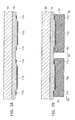
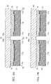
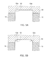
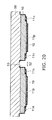
- FIGS. 3A and 3B to FIGS. 11A and 11B are cross-sectional views of processes, showing the method for manufacturing the semiconductor light emitting device according to the embodiment.
- a substrate 50 for the crystal growth is prepared.
- the substrate 50 includes, for example, a silicon wafer.
- the semiconductor layer 10 in which the n-type clad layer, the active layer, and the p-type clad layer are stacked in this order is formed on the entire surface of the upper surface of the substrate 50 by epitaxial growth of, for example, gallium nitride (GaN).
- the thickness of the semiconductor layer 10 is set to be, for example, 4 to 5 ⁇ m.
- n-side electrode 11n is formed on the region of the upper surface of the semiconductor layer 10 where the n-type clad layer is exposed; and the p-side electrode 11p is formed on the region of the upper surface of the semiconductor layer 10 where the p-type clad layer remains.
- a resist pattern 51 is formed on the semiconductor layer 10.
- the resist pattern 51 is divided into multiple portions for each region where the semiconductor light emitting device 1 is to be formed such that the portions are arranged, for example, in a matrix configuration.
- a region 52 that is not covered with the portions of the resist pattern 51 has, for example, a lattice configuration and includes a region to be used as a dicing line in a subsequent process.
- the semiconductor layer 10 and the substrate 50 are selectively removed by performing dry etching such as RIE (reactive ion etching), etc., using the resist pattern 51 as a mask.
- dry etching such as RIE (reactive ion etching), etc.
- the semiconductor layer 10 is divided into multiple portions; and a trench 53 is made in the upper surface of the substrate 50.
- the trench 53 is made in the region 52; and the depth of the trench 53, i.e., the distance from the interface between the substrate 50 and the semiconductor layer 10 to the bottom surface of the trench 53, is, for example, 3 to 5 ⁇ m.
- Each of the portions of the semiconductor layer 10 is patterned into a rectangle as viewed from above; and the n-type clad layer is exposed at the four corners.
- the semiconductor layer 10 is patterned into a high mesa.
- corners 53a of the trench 53 are sharp.
- the side surface of the trench 53 may be tilted such that the width of the trench 53 becomes narrower downward by adjusting the conditions of the dry etching.
- wet etching is performed using the resist pattern 51 as a mask.
- the corners 53a of the trench 53 are rounded.
- the curvature radii r of the corners 53a are set to be 1 ⁇ m or more.
- the resist pattern 51 (referring to FIG. 4B ) is removed.
- the passivation film 19 is formed on the entire surface by depositing an insulating material, e.g., silicon oxide or silicon nitride.
- the passivation film 19 also is formed on the inner surface of the trench 53 of the substrate 50.
- the passivation film 19 is patterned to make the hole 19n that communicates with the n-side electrode 11n and the hole 19p that communicates with the p-side electrode 11p.
- a seed layer (not shown) of copper is formed on the entire surface.
- a resist pattern 54 is formed in the region where the interconnect layer 13 is not to be formed in a subsequent process.
- the resist pattern 54 is disposed inside the outer edge of the n-side electrode 11n or inside the outer edge of the p-side electrode 11p as viewed from below.
- copper is deposited by, for example, electroplating. Thereby, the interconnect layer 13 is formed in the region where the resist pattern 54 is not disposed.
- the portion 13n of the interconnect layer 13 is connected to the n-side electrode 11n via the hole 19n; and the portion 13p is connected to the p-side electrode 11p via the hole 19p. Also, the portion 13s is formed on the side surface of the semiconductor layer 10 to cover the corner 53a of the trench 53.
- the resist pattern 54 By disposing the resist pattern 54 inside the outer edge of the n-side electrode 11n or inside the outer edge of the p-side electrode 11p as viewed from below, the end portion of the interconnect layer 13 overlaps the end portion of the n-side electrode 11n and the end portion of the p-side electrode 11p. Subsequently, the resist pattern 54 is removed.
- the n-side pillar 14n and the p-side pillar 14p are formed by selectively depositing, for example, copper.
- the n-side pillar 14n is connected to the portion 13n of the interconnect layer 13; and the p-side pillar 14p is connected to the portion 13p of the interconnect layer 13.
- the seed layer is removed by performing etching of the entire surface.
- the interconnect layer 13 is divided into multiple portions; and the portion 13n and the portion 13p are insulated from each other.
- a black resin is coated onto the entire surface of the substrate 50 to cover the n-side pillar 14n and the p-side pillar 14p. Thereby, the black resin portion 15 is formed.
- the sealing member 12 is formed of the interconnect layer 13, the n-side pillar 14n, the p-side pillar 14p, and the black resin portion 15.
- the substrate 50 (referring to FIG. 8B ) is removed. Thereby, the surface of the semiconductor layer 10 that contacted the substrate 50 is exposed.
- the notation of up and down is reversed to match the drawings.
- an unevenness is formed in the exposed surface of the semiconductor layer 10, i.e., the upper surface 10a.
- the adhesion layer 17 is formed by depositing silicon oxide on the entire surface on the upper surface of the sealing member 12 that opposed the substrate 50 and on the upper surface 10a of the semiconductor layer 10.
- the fluorescer layer 18 is formed on the adhesion layer 17. At this time, the fluorescer layer 18 is heated to, for example, about 170 °C.
- dicing is performed along the dicing line set inside the region 52.
- a dicing blade 55 passes through the trench 53.
- the fluorescer layer 18 and the black resin portion 15 are singulated for each semiconductor layer 10; and multiple semiconductor light emitting devices 1 (referring to FIGS. 1A and 1B ) are manufactured collectively.
- FIG. 12 is a plan view showing a method for manufacturing a semiconductor light emitting device according to a comparative example.
- FIG. 12 corresponds to the process shown in FIG. 10B .
- FIG. 12 shows the state directly after the fluorescer layer 18 is formed.
- the fluorescer layer 18 is not shown in FIG. 12 .
- FIG. 4B and FIG. 5B are omitted from the method for manufacturing the semiconductor light emitting device according to the comparative example.
- the corners 53a of the trench 53 of the substrate 50 are not rounded; and accordingly, the corners 12b of the protruding portion 12a of the sealing member 12 are not rounded.
- the corners 12b of the protruding portion 12a are rounded as shown in FIG. 2A by rounding the corners 53a of the trench 53 in the processes shown in FIG. 4B and FIG. 5B .
- the stress applied to the passivation film 19 from the sealing member 12 does not concentrate easily at the corners 12b; and the occurrence of the cracks 60 having the corners 12b as starting points can be suppressed.
- the reliability of the semiconductor light emitting device 1 can be improved.
- the semiconductor light emitting device 1 was modeled to simulate the internal stress distribution of the passivation film 19.
- FIG. 13A shows the model of the semiconductor light emitting device assumed in the simulation
- FIG. 13B shows the simulation result using the model of FIG. 13A .
- FIG. 14A is a partially-enlarged view of FIG. 13A ; and FIG. 14B is a partially-enlarged view of FIG. 13B .
- the semiconductor layer 10 was formed of gallium nitride (GaN); the resin portion (the black resin portion 15) of the sealing member 12 was formed of a black resin; the metal portion (the interconnect layer 13, the n-side pillar 14n, and the p-side pillar 14p) of the sealing member 12 was formed of copper (Cu); and the passivation film 19 was formed of silicon nitride (SiN).
- the width of the protruding portion 12a of the sealing member 12 was 80 ⁇ m; the height of the protruding portion 12a using the upper surface 10a of the semiconductor layer 10 as a reference was 3 ⁇ m; the tilt angle of the protruding portion 12a side surface 12c using the upper surface 10a as a reference was 75 degrees; and the thickness of the passivation film 19 was 400 nm.
- the corner 12b of the protruding portion 12a was formed of a black resin. The corner 12b was not rounded. In other words, the curvature radius r of the corner 12b was 0.
- the stress distribution of the passivation film 19 had peaks at the vicinity of the corner 12b of the protruding portion 12a and at the vicinity of the boundary between the resin portion and the metal portion of the sealing member 12; and the maximum stress at the corner 12b vicinity was 115 MPa.
- FIG. 15A shows a model of the semiconductor light emitting device assumed in the simulation
- FIG. 15B shows the simulation result using the model of FIG. 15A .
- the model assumed in the simulation differs from the first simulation described above in that the corner 12b of the protruding portion 12a was formed of copper. According to the simulation, it is possible to substantially simulate the case where a light-shielding film, i.e., the portion 13s of the interconnect layer 13, is disposed at the corner 12b of the protruding portion 12a.
- the stress distribution of the passivation film 19 was concentrated at the corner 12b vicinity in the case where the corner 12b was not rounded. Therefore, it is considered that the cracks 60 occur in the passivation film 19 with the corner 12b vicinity as a starting point.
- the end portion of the interconnect layer 13 extends onto the end portion of the n-side electrode 11n with the passivation film 19 interposed.
- the interconnect layer 13, the n-side electrode 11n, and the p-side electrode 11p are set to overlap, the light that is emitted from the semiconductor layer 10 and the fluorescer layer 18 toward the black resin portion 15 is reflected and extracted outside the semiconductor light emitting device 1. Thereby, the output of the light can be increased because the light that originally would be absorbed by the black resin portion 15 can be utilized effectively.
- the portion 13s is formed integrally with the portion 13n.
- the portion 13s can be formed to cover the entire circumference of the side surface of the semiconductor layer 10 in a ring configuration (an 0-shape). Thereby, gaps that leak the light emitted from the semiconductor layer 10 are favorably reduced.
- portion 13s is formed integrally with the portion 13n, the portion 13s that is used as the light-shielding film is connected to the outside via the portion 13n and the n-side pillar 14n. Thereby, the heat dissipation path of (portion 13s ⁇ portion 13n ⁇ n-side pillar 14n) is formed; and the heat dissipation of the semiconductor layer 10 improves.
- the portion 13n, the portion 13p, and the portion 13s of the interconnect layer 13 may be separated from each other. In such a case as well, the gaps are favorably reduced because the portion 13s can cover the entire circumference of the side surface of the semiconductor layer 10 in the ring configuration (the O-shape).
- Part of the portion 13s may be formed integrally with the portion 13n; and the remainder of the portion 13s may be formed integrally with the portion 13p and insulated from the part of the portion 13s.
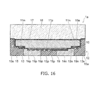
- FIG. 16 is a cross-sectional view showing a semiconductor light emitting device according to the modification.
- the portion 13s of the interconnect layer 13 is separated from the portion 13n.
- the portion 13n that functions as the light-shielding film is insulated from both the n-side electrode 11n and the p-side electrode 11p.
- the configuration, the manufacturing method, and the effects of the modification are similar to those of the first embodiment described above.
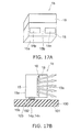
- FIG. 17A is a perspective view showing a semiconductor light emitting device according to the modification; and FIG. 17B is a side view showing the state in which the semiconductor light emitting device is mounted to a mounting substrate.
- the n-side pillar 14n and the p-side pillar 14p are exposed not at the lower surface 15a of the black resin portion 15 but at a side surface 15b of the black resin portion 15.
- the side surface 15b of the black resin portion 15 is a surface included in the same plane as the side surface of the fluorescer layer 18.
- the semiconductor light emitting device 1b When the semiconductor light emitting device 1b is mounted to a mounting substrate 100 as shown in FIG. 17B , the n-side pillar 14n and the p-side pillar 14p that are exposed at the side surface 15b of the black resin portion 15 of the semiconductor light emitting device 1b are connected by solder 103 to two electrode pads 102 provided in a mounting surface 101 of the mounting substrate 100. Thereby, the light emitting surface of the semiconductor light emitting device 1b, i.e., the upper surface of the fluorescer layer 18, is substantially perpendicular to the mounting surface 101 of the mounting substrate 100. As a result, the semiconductor light emitting device 1b can emit light mainly in a direction parallel to the mounting surface 101. Otherwise, the configuration, the manufacturing method, and the effects of the modification are similar to those of the first embodiment described above.
- FIG. 18 is a process plan view showing a method for manufacturing a semiconductor light emitting device according to the embodiment.
- FIG. 18 corresponds to the process shown in FIG. 4A .
- the components other than the substrate 50 and the semiconductor layer 10 are not shown.
- the corners of the portions are rounded when the semiconductor layer 10 is divided by patterning.
- the configuration of the semiconductor layer 10 included in one semiconductor light emitting device is a rectangle that has rounded corners as viewed from above.
- the corners of the semiconductor layer 10 may be rounded in the first embodiment described above as well. Thereby, the occurrence of the cracks of the passivation film 19 can be more effectively suppressed. As a result, the reliability of the semiconductor light emitting device can be improved even more.
- FIG. 19A is a cross-sectional view showing a semiconductor light emitting device according to the embodiment.
- FIG. 19B is a partially-enlarged cross-sectional view showing region C of FIG. 19A .
- the passivation film 19 is not provided; and the black resin portion 15 contacts the fluorescer layer 18.
- the semiconductor light emitting device 3 differs from the semiconductor light emitting device 1 in that the corner 12b of the protruding portion 12a of the sealing member 12 is not rounded. Also, the side surface 12c of the protruding portion 12a of the sealing member 12 opposing the semiconductor layer 10 is perpendicular to the upper surface 10a of the semiconductor layer 10.
- FIG. 20 is a cross-sectional view of a process, showing the method for manufacturing the semiconductor light emitting device according to the embodiment.
- FIG. 3A, FIG. 3B , and FIG. 4A are implemented. However, the wet etching process shown in FIG. 4B is omitted. Then, the n-side electrode 11n, the p-side electrode 11p, and the passivation film 19 are formed by implementing the processes shown in FIGS. 6A and 6B .
- RIE is performed to remove the passivation film 19 from the region 52 where the dicing line is to be set. Thereby, the passivation film 19 is divided for every semiconductor layer 10.
- the passivation film 19 is divided for every semiconductor layer 10 in the process shown in FIG. 20 .
- the internal stress of the passivation film 19 can be relaxed; and the warp of the silicon wafer used to form the substrate 50 for crystal growth or the resin wafer used to form the sealing member 12 can be reduced.
- the thermal stress between the passivation film 19 and the substrate 50 and the thermal stress between the passivation film 19 and the sealing member 12 can be reduced from an amount corresponding to the wafer size to an amount corresponding to the chip size; and the warp that is due to the thermal stress can be reduced.
- the manufacturing processes easy but also the stress remaining in the semiconductor light emitting device 3 after completion decreases; and the occurrence of the cracks 60 (referring to FIG. 12 ) can be suppressed.
- the embodiment may be combined with other embodiments and modifications of other embodiments.
- the corner 12b of the protruding portion 12a of the sealing member 12 (referring to FIG. 2A ) may be rounded.
- the side surface 12c of the protruding portion 12a may be tilted with respect to the perpendicular surface.
- FIG. 21A is a cross-sectional view showing a semiconductor light emitting device according to the embodiment.
- FIG. 21B is a bottom view of FIG. 21A .
- FIG. 22A is a partially-enlarged cross-sectional view showing region D of FIG. 21A ; and FIG. 22B is a partially-enlarged plan view showing region E of FIG. 21B .
- FIG. 21B and FIG. 22B only the semiconductor layer 10, the n-side electrode 11n, the p-side electrode 11p, and the interconnect layer 13 are shown for easier viewing of the drawing. Also, the edge lines that illustrate the configurations of these members are not shown.
- the end portion of the interconnect layer 13 extends to partially overlap the n-side electrode 11n and the p-side electrode 11p with the passivation film 19 interposed. Therefore, substantially the entire semiconductor layer 10 is covered with the n-side electrode 11n, the p-side electrode 11p, and the interconnect layer 13 as viewed from below and from the side.
- the semiconductor light emitting device 4 differs from the semiconductor light emitting device 1 in that the corner 12b of the protruding portion 12a of the sealing member 12 (referring to FIG. 2A ) is not rounded. Such a configuration is formed by omitting the wet etching process shown in FIG. 4B . Also, the portion 13n, the portion 13p, and the portion 13s of the interconnect layer 13 are separated from each other in the semiconductor light emitting device 4.
- the light emitted from the semiconductor layer 10 and the fluorescer layer 18 that is incident on the black resin portion 15 can be suppressed; and the degradation of the black resin portion 15 can be suppressed. Also, because the light can be extracted efficiently, the output of the light can be increased.
- the portion 13n, the portion 13p, and the portion 13s of the interconnect layer 13 are separated from each other.
- the portion 13s can be formed in a ring configuration (an O-shape) to continuously cover the entire circumference of the side surface of the semiconductor layer 10. Thereby, the gaps that leak the light emitted from the semiconductor layer 10 can be reduced effectively.
- the portion 13s may be formed integrally with the portion 13p or the portion 13n. By such a method as well, the portion 13s can be formed in a ring configuration. Further, part of the portion 13s may be formed integrally with the portion 13n; and the remainder of the portion 13s may be formed integrally with the portion 13p and insulated from the part of the portion 13s.
- the manufacturing cost can be reduced because the wet etching process shown in FIG. 4B is omitted. Otherwise, the configuration and the manufacturing method of the embodiment are similar to those of the first embodiment described above.
- the black resin portion 15 is not limited thereto and may be formed of resins of other colors.
- a white resin may be used.
- a semiconductor light emitting device and a method for manufacturing the semiconductor light emitting device having high reliability can be realized.
Landscapes
- Led Device Packages (AREA)
- Led Devices (AREA)
Applications Claiming Priority (2)
| Application Number | Priority Date | Filing Date | Title |
|---|---|---|---|
| JP2013188558 | 2013-09-11 | ||
| JP2014064515A JP2015079929A (ja) | 2013-09-11 | 2014-03-26 | 半導体発光装置及びその製造方法 |
Publications (3)
| Publication Number | Publication Date |
|---|---|
| EP2858129A2 true EP2858129A2 (de) | 2015-04-08 |
| EP2858129A3 EP2858129A3 (de) | 2015-06-17 |
| EP2858129B1 EP2858129B1 (de) | 2018-12-12 |
Family
ID=51176269
Family Applications (1)
| Application Number | Title | Priority Date | Filing Date |
|---|---|---|---|
| EP14177043.8A Active EP2858129B1 (de) | 2013-09-11 | 2014-07-15 | Lichtemittierendes Halbleiterbauelement |
Country Status (6)
| Country | Link |
|---|---|
| US (1) | US9887328B2 (de) |
| EP (1) | EP2858129B1 (de) |
| JP (1) | JP2015079929A (de) |
| KR (1) | KR101662384B1 (de) |
| HK (1) | HK1207471A1 (de) |
| TW (1) | TWI542044B (de) |
Cited By (1)
| Publication number | Priority date | Publication date | Assignee | Title |
|---|---|---|---|---|
| WO2021028233A1 (de) * | 2019-08-12 | 2021-02-18 | Osram Opto Semiconductors Gmbh | Halbleiterbauelement und dessen herstellungsverfahren |
Families Citing this family (3)
| Publication number | Priority date | Publication date | Assignee | Title |
|---|---|---|---|---|
| JP2015079929A (ja) * | 2013-09-11 | 2015-04-23 | 株式会社東芝 | 半導体発光装置及びその製造方法 |
| KR102652087B1 (ko) * | 2016-12-16 | 2024-03-28 | 삼성전자주식회사 | 반도체 발광소자 |
| WO2019164449A1 (en) * | 2018-02-22 | 2019-08-29 | Massachusetts Institute Of Technology | Method of reducing semiconductor substrate surface unevenness |
Family Cites Families (23)
| Publication number | Priority date | Publication date | Assignee | Title |
|---|---|---|---|---|
| JP2699517B2 (ja) | 1988-02-24 | 1998-01-19 | モトローラ・インコーポレーテッド | 丸形またはテーパ状エッジおよびコーナーを有する半導体デバイス |
| JP3496925B2 (ja) | 1998-02-04 | 2004-02-16 | キヤノン株式会社 | 半導体基板とその製造方法 |
| JP3946107B2 (ja) | 2002-07-03 | 2007-07-18 | 株式会社リコー | 半導体装置の製造装置及び半導体装置の製造方法 |
| JP4285079B2 (ja) | 2003-05-22 | 2009-06-24 | カシオ計算機株式会社 | 半導体装置の製造方法 |
| JP4238666B2 (ja) | 2003-07-17 | 2009-03-18 | 豊田合成株式会社 | 発光装置の製造方法 |
| JP4474892B2 (ja) | 2003-10-14 | 2010-06-09 | 日亜化学工業株式会社 | フリップチップ型led |
| JP4103888B2 (ja) | 2004-12-03 | 2008-06-18 | ヤマハ株式会社 | 半導体装置 |
| JP4724222B2 (ja) | 2008-12-12 | 2011-07-13 | 株式会社東芝 | 発光装置の製造方法 |
| JP2011071272A (ja) | 2009-09-25 | 2011-04-07 | Toshiba Corp | 半導体発光装置及びその製造方法 |
| JP2011071444A (ja) | 2009-09-28 | 2011-04-07 | Toyoda Gosei Co Ltd | 発光素子 |
| WO2011102411A1 (ja) * | 2010-02-19 | 2011-08-25 | シャープ株式会社 | 窒化物半導体発光素子および窒化物半導体発光素子の製造方法 |
| JP5343040B2 (ja) * | 2010-06-07 | 2013-11-13 | 株式会社東芝 | 半導体発光装置 |
| KR20120066973A (ko) | 2010-12-15 | 2012-06-25 | 삼성엘이디 주식회사 | 발광 디바이스 및 그 제조방법 |
| JP5603813B2 (ja) * | 2011-03-15 | 2014-10-08 | 株式会社東芝 | 半導体発光装置及び発光装置 |
| JP4865101B2 (ja) | 2011-04-05 | 2012-02-01 | 株式会社東芝 | 半導体発光装置 |
| JP2013021175A (ja) | 2011-07-12 | 2013-01-31 | Toshiba Corp | 半導体発光素子 |
| JP5662277B2 (ja) * | 2011-08-08 | 2015-01-28 | 株式会社東芝 | 半導体発光装置及び発光モジュール |
| JP2013084889A (ja) | 2011-09-30 | 2013-05-09 | Toshiba Corp | 半導体発光装置及びその製造方法 |
| WO2013097046A1 (zh) | 2011-12-26 | 2013-07-04 | 璩泽明 | 电极共平面的发光二极管元件、封装结构及光反射结构 |
| JP2013042191A (ja) | 2012-11-30 | 2013-02-28 | Toshiba Corp | 半導体発光装置 |
| JP2015079929A (ja) * | 2013-09-11 | 2015-04-23 | 株式会社東芝 | 半導体発光装置及びその製造方法 |
| JP6219177B2 (ja) * | 2014-01-17 | 2017-10-25 | スタンレー電気株式会社 | 半導体発光装置 |
| TWI550909B (zh) * | 2014-03-21 | 2016-09-21 | 茂邦電子有限公司 | A flip chip type light emitting diode and a method for manufacturing the same, and a flip chip type structure thereof |
-
2014
- 2014-03-26 JP JP2014064515A patent/JP2015079929A/ja active Pending
- 2014-06-27 TW TW103122269A patent/TWI542044B/zh active
- 2014-07-10 US US14/328,048 patent/US9887328B2/en active Active
- 2014-07-15 EP EP14177043.8A patent/EP2858129B1/de active Active
- 2014-07-15 KR KR1020140089032A patent/KR101662384B1/ko active Active
-
2015
- 2015-08-17 HK HK15107904.3A patent/HK1207471A1/en unknown
Non-Patent Citations (1)
| Title |
|---|
| None |
Cited By (2)
| Publication number | Priority date | Publication date | Assignee | Title |
|---|---|---|---|---|
| WO2021028233A1 (de) * | 2019-08-12 | 2021-02-18 | Osram Opto Semiconductors Gmbh | Halbleiterbauelement und dessen herstellungsverfahren |
| US12453227B2 (en) | 2019-08-12 | 2025-10-21 | Osram Opto Semiconductors Gmbh | Semiconductor component and method for producing the same |
Also Published As
| Publication number | Publication date |
|---|---|
| KR101662384B1 (ko) | 2016-10-04 |
| US20150069437A1 (en) | 2015-03-12 |
| US9887328B2 (en) | 2018-02-06 |
| TWI542044B (zh) | 2016-07-11 |
| HK1207471A1 (en) | 2016-01-29 |
| EP2858129A3 (de) | 2015-06-17 |
| TW201519478A (zh) | 2015-05-16 |
| EP2858129B1 (de) | 2018-12-12 |
| KR20150030145A (ko) | 2015-03-19 |
| JP2015079929A (ja) | 2015-04-23 |
Similar Documents
| Publication | Publication Date | Title |
|---|---|---|
| US20230155072A1 (en) | Light emitting diode package and method of manufacturing the same | |
| TWI682558B (zh) | 半導體發光裝置 | |
| US9502627B2 (en) | Wafer level photonic devices dies structure and method of making the same | |
| JP5197654B2 (ja) | 半導体発光装置及びその製造方法 | |
| US10283685B2 (en) | Light emitting device and method of fabricating the same | |
| US20180309029A1 (en) | Light emitting device and method of fabricating the same | |
| KR20160113042A (ko) | 발광 다이오드를 포함하는 광전자 디바이스 | |
| JP2017055093A (ja) | 半導体発光装置 | |
| EP2858129B1 (de) | Lichtemittierendes Halbleiterbauelement | |
| KR20150069228A (ko) | 파장변환층을 갖는 발광 다이오드 및 그것을 제조하는 방법 | |
| US10553758B2 (en) | Semiconductor light emitting device | |
| US20170069792A1 (en) | Semiconductor light emitting device | |
| CN204792904U (zh) | 发光二极管芯片及发光装置 | |
| US20160211417A1 (en) | Semiconductor light-emitting element, light emitting device, and method of manufacturing semiconductor light-emitting element | |
| US9054288B2 (en) | Light emitting diode with high light extraction efficiency and method for manufacturing the same | |
| JP2015188039A (ja) | 半導体発光装置およびその製造方法 | |
| KR102217128B1 (ko) | 발광 다이오드 및 그 제조 방법 | |
| JP5426788B2 (ja) | 半導体発光装置 | |
| KR20130142581A (ko) | 개선된 광 추출 효율을 갖는 발광 소자 및 그것을 제조하는 방법 | |
| KR102001663B1 (ko) | 발광 다이오드 패키지 | |
| KR20150037215A (ko) | 넓은 지향각을 갖는 발광 소자 및 그 제조 방법 | |
| KR20120111391A (ko) | 발광 다이오드 칩 및 그의 제조 방법 | |
| KR20150112236A (ko) | 발광 다이오드 및 그 제조 방법 | |
| KR20130122158A (ko) | 발광 소자 패키지 및 그 제조방법 |
Legal Events
| Date | Code | Title | Description |
|---|---|---|---|
| PUAI | Public reference made under article 153(3) epc to a published international application that has entered the european phase |
Free format text: ORIGINAL CODE: 0009012 |
|
| 17P | Request for examination filed |
Effective date: 20140715 |
|
| AK | Designated contracting states |
Kind code of ref document: A2 Designated state(s): AL AT BE BG CH CY CZ DE DK EE ES FI FR GB GR HR HU IE IS IT LI LT LU LV MC MK MT NL NO PL PT RO RS SE SI SK SM TR |
|
| AX | Request for extension of the european patent |
Extension state: BA ME |
|
| PUAL | Search report despatched |
Free format text: ORIGINAL CODE: 0009013 |
|
| AK | Designated contracting states |
Kind code of ref document: A3 Designated state(s): AL AT BE BG CH CY CZ DE DK EE ES FI FR GB GR HR HU IE IS IT LI LT LU LV MC MK MT NL NO PL PT RO RS SE SI SK SM TR |
|
| AX | Request for extension of the european patent |
Extension state: BA ME |
|
| RIC1 | Information provided on ipc code assigned before grant |
Ipc: H01L 33/46 20100101AFI20150508BHEP Ipc: H01L 33/54 20100101ALI20150508BHEP Ipc: H01L 33/60 20100101ALN20150508BHEP Ipc: H01L 33/50 20100101ALN20150508BHEP Ipc: H01L 33/00 20100101ALN20150508BHEP |
|
| REG | Reference to a national code |
Ref country code: HK Ref legal event code: DE Ref document number: 1207471 Country of ref document: HK |
|
| STAA | Information on the status of an ep patent application or granted ep patent |
Free format text: STATUS: EXAMINATION IS IN PROGRESS |
|
| 17Q | First examination report despatched |
Effective date: 20180329 |
|
| GRAP | Despatch of communication of intention to grant a patent |
Free format text: ORIGINAL CODE: EPIDOSNIGR1 |
|
| STAA | Information on the status of an ep patent application or granted ep patent |
Free format text: STATUS: GRANT OF PATENT IS INTENDED |
|
| RAP1 | Party data changed (applicant data changed or rights of an application transferred) |
Owner name: TOSHIBA ELECTRONIC DEVICES & STORAGE CORPORATION |
|
| RIC1 | Information provided on ipc code assigned before grant |
Ipc: H01L 33/54 20100101ALI20180629BHEP Ipc: H01L 33/46 20100101AFI20180629BHEP Ipc: H01L 33/60 20100101ALN20180629BHEP Ipc: H01L 33/50 20100101ALN20180629BHEP Ipc: H01L 33/00 20100101ALN20180629BHEP |
|
| INTG | Intention to grant announced |
Effective date: 20180719 |
|
| RAP1 | Party data changed (applicant data changed or rights of an application transferred) |
Owner name: SAMSUNG ELECTRONICS CO., LTD. |
|
| GRAS | Grant fee paid |
Free format text: ORIGINAL CODE: EPIDOSNIGR3 |
|
| GRAA | (expected) grant |
Free format text: ORIGINAL CODE: 0009210 |
|
| STAA | Information on the status of an ep patent application or granted ep patent |
Free format text: STATUS: THE PATENT HAS BEEN GRANTED |
|
| AK | Designated contracting states |
Kind code of ref document: B1 Designated state(s): AL AT BE BG CH CY CZ DE DK EE ES FI FR GB GR HR HU IE IS IT LI LT LU LV MC MK MT NL NO PL PT RO RS SE SI SK SM TR |
|
| REG | Reference to a national code |
Ref country code: GB Ref legal event code: FG4D |
|
| REG | Reference to a national code |
Ref country code: CH Ref legal event code: EP |
|
| REG | Reference to a national code |
Ref country code: AT Ref legal event code: REF Ref document number: 1077138 Country of ref document: AT Kind code of ref document: T Effective date: 20181215 |
|
| REG | Reference to a national code |
Ref country code: DE Ref legal event code: R096 Ref document number: 602014037730 Country of ref document: DE |
|
| REG | Reference to a national code |
Ref country code: IE Ref legal event code: FG4D |
|
| REG | Reference to a national code |
Ref country code: NL Ref legal event code: FP |
|
| REG | Reference to a national code |
Ref country code: LT Ref legal event code: MG4D |
|
| PG25 | Lapsed in a contracting state [announced via postgrant information from national office to epo] |
Ref country code: LV Free format text: LAPSE BECAUSE OF FAILURE TO SUBMIT A TRANSLATION OF THE DESCRIPTION OR TO PAY THE FEE WITHIN THE PRESCRIBED TIME-LIMIT Effective date: 20181212 Ref country code: ES Free format text: LAPSE BECAUSE OF FAILURE TO SUBMIT A TRANSLATION OF THE DESCRIPTION OR TO PAY THE FEE WITHIN THE PRESCRIBED TIME-LIMIT Effective date: 20181212 Ref country code: LT Free format text: LAPSE BECAUSE OF FAILURE TO SUBMIT A TRANSLATION OF THE DESCRIPTION OR TO PAY THE FEE WITHIN THE PRESCRIBED TIME-LIMIT Effective date: 20181212 Ref country code: NO Free format text: LAPSE BECAUSE OF FAILURE TO SUBMIT A TRANSLATION OF THE DESCRIPTION OR TO PAY THE FEE WITHIN THE PRESCRIBED TIME-LIMIT Effective date: 20190312 Ref country code: FI Free format text: LAPSE BECAUSE OF FAILURE TO SUBMIT A TRANSLATION OF THE DESCRIPTION OR TO PAY THE FEE WITHIN THE PRESCRIBED TIME-LIMIT Effective date: 20181212 Ref country code: BG Free format text: LAPSE BECAUSE OF FAILURE TO SUBMIT A TRANSLATION OF THE DESCRIPTION OR TO PAY THE FEE WITHIN THE PRESCRIBED TIME-LIMIT Effective date: 20190312 Ref country code: HR Free format text: LAPSE BECAUSE OF FAILURE TO SUBMIT A TRANSLATION OF THE DESCRIPTION OR TO PAY THE FEE WITHIN THE PRESCRIBED TIME-LIMIT Effective date: 20181212 |
|
| REG | Reference to a national code |
Ref country code: AT Ref legal event code: MK05 Ref document number: 1077138 Country of ref document: AT Kind code of ref document: T Effective date: 20181212 |
|
| PG25 | Lapsed in a contracting state [announced via postgrant information from national office to epo] |
Ref country code: GR Free format text: LAPSE BECAUSE OF FAILURE TO SUBMIT A TRANSLATION OF THE DESCRIPTION OR TO PAY THE FEE WITHIN THE PRESCRIBED TIME-LIMIT Effective date: 20190313 Ref country code: RS Free format text: LAPSE BECAUSE OF FAILURE TO SUBMIT A TRANSLATION OF THE DESCRIPTION OR TO PAY THE FEE WITHIN THE PRESCRIBED TIME-LIMIT Effective date: 20181212 Ref country code: SE Free format text: LAPSE BECAUSE OF FAILURE TO SUBMIT A TRANSLATION OF THE DESCRIPTION OR TO PAY THE FEE WITHIN THE PRESCRIBED TIME-LIMIT Effective date: 20181212 Ref country code: AL Free format text: LAPSE BECAUSE OF FAILURE TO SUBMIT A TRANSLATION OF THE DESCRIPTION OR TO PAY THE FEE WITHIN THE PRESCRIBED TIME-LIMIT Effective date: 20181212 |
|
| PG25 | Lapsed in a contracting state [announced via postgrant information from national office to epo] |
Ref country code: PL Free format text: LAPSE BECAUSE OF FAILURE TO SUBMIT A TRANSLATION OF THE DESCRIPTION OR TO PAY THE FEE WITHIN THE PRESCRIBED TIME-LIMIT Effective date: 20181212 Ref country code: IT Free format text: LAPSE BECAUSE OF FAILURE TO SUBMIT A TRANSLATION OF THE DESCRIPTION OR TO PAY THE FEE WITHIN THE PRESCRIBED TIME-LIMIT Effective date: 20181212 Ref country code: CZ Free format text: LAPSE BECAUSE OF FAILURE TO SUBMIT A TRANSLATION OF THE DESCRIPTION OR TO PAY THE FEE WITHIN THE PRESCRIBED TIME-LIMIT Effective date: 20181212 Ref country code: PT Free format text: LAPSE BECAUSE OF FAILURE TO SUBMIT A TRANSLATION OF THE DESCRIPTION OR TO PAY THE FEE WITHIN THE PRESCRIBED TIME-LIMIT Effective date: 20190412 |
|
| PG25 | Lapsed in a contracting state [announced via postgrant information from national office to epo] |
Ref country code: RO Free format text: LAPSE BECAUSE OF FAILURE TO SUBMIT A TRANSLATION OF THE DESCRIPTION OR TO PAY THE FEE WITHIN THE PRESCRIBED TIME-LIMIT Effective date: 20181212 Ref country code: IS Free format text: LAPSE BECAUSE OF FAILURE TO SUBMIT A TRANSLATION OF THE DESCRIPTION OR TO PAY THE FEE WITHIN THE PRESCRIBED TIME-LIMIT Effective date: 20190412 Ref country code: EE Free format text: LAPSE BECAUSE OF FAILURE TO SUBMIT A TRANSLATION OF THE DESCRIPTION OR TO PAY THE FEE WITHIN THE PRESCRIBED TIME-LIMIT Effective date: 20181212 Ref country code: SM Free format text: LAPSE BECAUSE OF FAILURE TO SUBMIT A TRANSLATION OF THE DESCRIPTION OR TO PAY THE FEE WITHIN THE PRESCRIBED TIME-LIMIT Effective date: 20181212 Ref country code: SK Free format text: LAPSE BECAUSE OF FAILURE TO SUBMIT A TRANSLATION OF THE DESCRIPTION OR TO PAY THE FEE WITHIN THE PRESCRIBED TIME-LIMIT Effective date: 20181212 |
|
| REG | Reference to a national code |
Ref country code: DE Ref legal event code: R097 Ref document number: 602014037730 Country of ref document: DE |
|
| PLBE | No opposition filed within time limit |
Free format text: ORIGINAL CODE: 0009261 |
|
| STAA | Information on the status of an ep patent application or granted ep patent |
Free format text: STATUS: NO OPPOSITION FILED WITHIN TIME LIMIT |
|
| PG25 | Lapsed in a contracting state [announced via postgrant information from national office to epo] |
Ref country code: DK Free format text: LAPSE BECAUSE OF FAILURE TO SUBMIT A TRANSLATION OF THE DESCRIPTION OR TO PAY THE FEE WITHIN THE PRESCRIBED TIME-LIMIT Effective date: 20181212 Ref country code: AT Free format text: LAPSE BECAUSE OF FAILURE TO SUBMIT A TRANSLATION OF THE DESCRIPTION OR TO PAY THE FEE WITHIN THE PRESCRIBED TIME-LIMIT Effective date: 20181212 Ref country code: SI Free format text: LAPSE BECAUSE OF FAILURE TO SUBMIT A TRANSLATION OF THE DESCRIPTION OR TO PAY THE FEE WITHIN THE PRESCRIBED TIME-LIMIT Effective date: 20181212 |
|
| 26N | No opposition filed |
Effective date: 20190913 |
|
| PG25 | Lapsed in a contracting state [announced via postgrant information from national office to epo] |
Ref country code: MC Free format text: LAPSE BECAUSE OF FAILURE TO SUBMIT A TRANSLATION OF THE DESCRIPTION OR TO PAY THE FEE WITHIN THE PRESCRIBED TIME-LIMIT Effective date: 20181212 |
|
| REG | Reference to a national code |
Ref country code: CH Ref legal event code: PL |
|
| PG25 | Lapsed in a contracting state [announced via postgrant information from national office to epo] |
Ref country code: TR Free format text: LAPSE BECAUSE OF FAILURE TO SUBMIT A TRANSLATION OF THE DESCRIPTION OR TO PAY THE FEE WITHIN THE PRESCRIBED TIME-LIMIT Effective date: 20181212 |
|
| REG | Reference to a national code |
Ref country code: BE Ref legal event code: MM Effective date: 20190731 |
|
| PG25 | Lapsed in a contracting state [announced via postgrant information from national office to epo] |
Ref country code: CH Free format text: LAPSE BECAUSE OF NON-PAYMENT OF DUE FEES Effective date: 20190731 Ref country code: BE Free format text: LAPSE BECAUSE OF NON-PAYMENT OF DUE FEES Effective date: 20190731 Ref country code: LI Free format text: LAPSE BECAUSE OF NON-PAYMENT OF DUE FEES Effective date: 20190731 Ref country code: LU Free format text: LAPSE BECAUSE OF NON-PAYMENT OF DUE FEES Effective date: 20190715 |
|
| PG25 | Lapsed in a contracting state [announced via postgrant information from national office to epo] |
Ref country code: IE Free format text: LAPSE BECAUSE OF NON-PAYMENT OF DUE FEES Effective date: 20190715 |
|
| PG25 | Lapsed in a contracting state [announced via postgrant information from national office to epo] |
Ref country code: CY Free format text: LAPSE BECAUSE OF FAILURE TO SUBMIT A TRANSLATION OF THE DESCRIPTION OR TO PAY THE FEE WITHIN THE PRESCRIBED TIME-LIMIT Effective date: 20181212 |
|
| PG25 | Lapsed in a contracting state [announced via postgrant information from national office to epo] |
Ref country code: MT Free format text: LAPSE BECAUSE OF FAILURE TO SUBMIT A TRANSLATION OF THE DESCRIPTION OR TO PAY THE FEE WITHIN THE PRESCRIBED TIME-LIMIT Effective date: 20181212 Ref country code: HU Free format text: LAPSE BECAUSE OF FAILURE TO SUBMIT A TRANSLATION OF THE DESCRIPTION OR TO PAY THE FEE WITHIN THE PRESCRIBED TIME-LIMIT; INVALID AB INITIO Effective date: 20140715 |
|
| REG | Reference to a national code |
Ref country code: HK Ref legal event code: WD Ref document number: 1207471 Country of ref document: HK |
|
| PG25 | Lapsed in a contracting state [announced via postgrant information from national office to epo] |
Ref country code: MK Free format text: LAPSE BECAUSE OF FAILURE TO SUBMIT A TRANSLATION OF THE DESCRIPTION OR TO PAY THE FEE WITHIN THE PRESCRIBED TIME-LIMIT Effective date: 20181212 |
|
| P01 | Opt-out of the competence of the unified patent court (upc) registered |
Effective date: 20230520 |
|
| REG | Reference to a national code |
Ref country code: DE Ref legal event code: R079 Ref document number: 602014037730 Country of ref document: DE Free format text: PREVIOUS MAIN CLASS: H01L0033460000 Ipc: H10H0020841000 |
|
| PGFP | Annual fee paid to national office [announced via postgrant information from national office to epo] |
Ref country code: NL Payment date: 20250526 Year of fee payment: 12 |
|
| PGFP | Annual fee paid to national office [announced via postgrant information from national office to epo] |
Ref country code: GB Payment date: 20250522 Year of fee payment: 12 |
|
| PGFP | Annual fee paid to national office [announced via postgrant information from national office to epo] |
Ref country code: FR Payment date: 20250523 Year of fee payment: 12 |
|
| PGFP | Annual fee paid to national office [announced via postgrant information from national office to epo] |
Ref country code: DE Payment date: 20250528 Year of fee payment: 12 |