EP2851965B1 - Solarzellen mit mehreren Anschlüssen - Google Patents
Solarzellen mit mehreren Anschlüssen Download PDFInfo
- Publication number
- EP2851965B1 EP2851965B1 EP14182810.3A EP14182810A EP2851965B1 EP 2851965 B1 EP2851965 B1 EP 2851965B1 EP 14182810 A EP14182810 A EP 14182810A EP 2851965 B1 EP2851965 B1 EP 2851965B1
- Authority
- EP
- European Patent Office
- Prior art keywords
- solar cell
- photoelectric conversion
- conversion devices
- layer
- regions
- Prior art date
- Legal status (The legal status is an assumption and is not a legal conclusion. Google has not performed a legal analysis and makes no representation as to the accuracy of the status listed.)
- Active
Links
Images







Classifications
-
- H—ELECTRICITY
- H10—SEMICONDUCTOR DEVICES; ELECTRIC SOLID-STATE DEVICES NOT OTHERWISE PROVIDED FOR
- H10F—INORGANIC SEMICONDUCTOR DEVICES SENSITIVE TO INFRARED RADIATION, LIGHT, ELECTROMAGNETIC RADIATION OF SHORTER WAVELENGTH OR CORPUSCULAR RADIATION
- H10F10/00—Individual photovoltaic cells, e.g. solar cells
- H10F10/10—Individual photovoltaic cells, e.g. solar cells having potential barriers
- H10F10/16—Photovoltaic cells having only PN heterojunction potential barriers
- H10F10/161—Photovoltaic cells having only PN heterojunction potential barriers comprising multiple PN heterojunctions, e.g. tandem cells
-
- H—ELECTRICITY
- H10—SEMICONDUCTOR DEVICES; ELECTRIC SOLID-STATE DEVICES NOT OTHERWISE PROVIDED FOR
- H10F—INORGANIC SEMICONDUCTOR DEVICES SENSITIVE TO INFRARED RADIATION, LIGHT, ELECTROMAGNETIC RADIATION OF SHORTER WAVELENGTH OR CORPUSCULAR RADIATION
- H10F10/00—Individual photovoltaic cells, e.g. solar cells
- H10F10/10—Individual photovoltaic cells, e.g. solar cells having potential barriers
- H10F10/14—Photovoltaic cells having only PN homojunction potential barriers
- H10F10/146—Back-junction photovoltaic cells, e.g. having interdigitated base-emitter regions on the back side
-
- H—ELECTRICITY
- H10—SEMICONDUCTOR DEVICES; ELECTRIC SOLID-STATE DEVICES NOT OTHERWISE PROVIDED FOR
- H10F—INORGANIC SEMICONDUCTOR DEVICES SENSITIVE TO INFRARED RADIATION, LIGHT, ELECTROMAGNETIC RADIATION OF SHORTER WAVELENGTH OR CORPUSCULAR RADIATION
- H10F19/00—Integrated devices, or assemblies of multiple devices, comprising at least one photovoltaic cell covered by group H10F10/00, e.g. photovoltaic modules
-
- H—ELECTRICITY
- H10—SEMICONDUCTOR DEVICES; ELECTRIC SOLID-STATE DEVICES NOT OTHERWISE PROVIDED FOR
- H10F—INORGANIC SEMICONDUCTOR DEVICES SENSITIVE TO INFRARED RADIATION, LIGHT, ELECTROMAGNETIC RADIATION OF SHORTER WAVELENGTH OR CORPUSCULAR RADIATION
- H10F19/00—Integrated devices, or assemblies of multiple devices, comprising at least one photovoltaic cell covered by group H10F10/00, e.g. photovoltaic modules
- H10F19/40—Integrated devices, or assemblies of multiple devices, comprising at least one photovoltaic cell covered by group H10F10/00, e.g. photovoltaic modules comprising photovoltaic cells in a mechanically stacked configuration
-
- Y—GENERAL TAGGING OF NEW TECHNOLOGICAL DEVELOPMENTS; GENERAL TAGGING OF CROSS-SECTIONAL TECHNOLOGIES SPANNING OVER SEVERAL SECTIONS OF THE IPC; TECHNICAL SUBJECTS COVERED BY FORMER USPC CROSS-REFERENCE ART COLLECTIONS [XRACs] AND DIGESTS
- Y02—TECHNOLOGIES OR APPLICATIONS FOR MITIGATION OR ADAPTATION AGAINST CLIMATE CHANGE
- Y02E—REDUCTION OF GREENHOUSE GAS [GHG] EMISSIONS, RELATED TO ENERGY GENERATION, TRANSMISSION OR DISTRIBUTION
- Y02E10/00—Energy generation through renewable energy sources
- Y02E10/50—Photovoltaic [PV] energy
- Y02E10/547—Monocrystalline silicon PV cells
Definitions
- Embodiments described herein relate to a multi-junction solar cell.
- High-efficiency solar cells include multi-junction (tandem type) solar cells. While the multi-junction solar cells are expected to be higher in efficiency than single-junction solar cells, the difference in the number of photons absorbed by each layer will produce a difference in current value to limit the conversion efficiency to that of the layer with the lowest value. This limit is unavoidable as long as a series junction is adopted. On the other hand, this limit can be avoided by extracting a terminal from each layer, while more than one power converter or the like will be required.
- EP 1 962 331 A2 discloses a thin-film solar cell comprising a first solar cell layer, a second solar cell layer and an electrode connector connecting the first solar cell layer with the second solar cell layer in parallel.
- a plurality of unit cells including a photoelectric conversion layer are connected in series.
- the first solar cell layer and the second solar cell layer are electrically separated from each other by an insulating layer therebetween.
- US 4,295,002 A discloses a solar cell with V-grooves which are series connected, but electrically isolated, indirect bandgap solar cells which are responsive to different light frequencies on both sides of a semi-insulating optically transparent substrate.
- the device has a very high conversion efficiency of approximately 40% and high open circuit voltage and low series resistance.
- An exemplary structure in accordance with the disclosure has a series of silicon V-groove cells on one side and another series of GaAlAs V-groove cells on the other side.
- the cells are of generally trapezoidal cross-section. The difference between the characteristics of the Si cell and the GaAlAs cell is matched by control of the number of V-grooves.
- the present invention is defined in independent claim 1.
- a multi-junction solar cell according to the present invention has the features of claim 1.
- a multi-junction solar cell has, as shown in FIG. 1 , a first solar cell A, an insulating layer C, and a second solar cell B.
- the insulating layer C is situated between the first solar cell A and the second solar cell B.
- a two-junction solar cell is adopted, but a three or more-junction solar cell may be adopted.
- the first solar cell A and the second solar cell B are connected in parallel.
- the lower electrodes 101 which are electrodes of the photoelectric conversion devices 100A to 100C, are conductive films formed on the insulating layer C.
- a conductive film integrally formed on the insulating layer C is divided by, for example, scribing into the lower electrodes 101 depending on the number of photoelectric conversion devices.
- Conductive and transparent films can be used as the lower electrodes 101.
- an ITO (Indium Tin Oxide ((In,Sn)O ⁇ , 1 ⁇ ⁇ ⁇ 3): Indium Tin Oxide) film as a transparent conductive film is desirably used for the lower electrodes 101.
- the lower electrodes 101 typically have a thickness of 100 nm to 1000 nm.
- the lower electrode 101 is connected to the adjacent upper electrode 103.
- the upper electrode 103 of the photoelectric conversion device 100A is connected to the lower electrode 101 of the photoelectric conversion device 100B, and the upper electrode 103 of the photoelectric conversion device B is connected to the lower electrode 101 of the photoelectric conversion device 100C.
- These connections between the lower electrodes 101 and the upper electrode 103 connect the three photoelectric conversion devices 100 in series. When the devices are not connected in series, these connections are not adopted. In the case of connections in parallel, the desired lower electrodes 101 may be connected to each other, whereas the desired upper electrodes 103 may be connected to each other.
- compound semiconductor layers which have wider gaps than photoelectric conversions of the second solar cells B can be used for the photoelectric conversion layers 102 of the first photoelectric conversion devices 100.
- CdS, etc. can be used as the n-type buffer layer.
- the chemical formulas which represent the compounds for the photoelectric conversion layers 102 include Cu(Al w In x Ga 1-w-x ) (S y Se z Te 1-y-z ) 2 and Cu 2 ZnSn(S y Se 1-y ) 4 .
- the w, x, y, and z respectively meet 0 ⁇ w ⁇ 1, 0 ⁇ x ⁇ 1, 0 ⁇ y ⁇ 1, 0 ⁇ z ⁇ 1, w + x ⁇ 1 and y + z ⁇ 1.
- the composition of the photoelectric conversion layer 102 can be measured by inductively-coupled plasma (ICP: Inductively Coupled Plasma) mass spectrometry.
- ICP Inductively Coupled Plasma
- the interlayer (not shown) is a compound thin film layer provided between the photoelectric conversion layer 102 and the upper electrode 103, or between the photoelectric conversion layer 102 and the window layer.
- photoelectric conversion devices are preferred include the interlayer, but the interlayer may be omitted.
- the interlayer may have the form of covering only some of the surfaces of the n-type compound semiconductor layers on the upper electrodes 103. For example, the interlayer only has to cover 50% of the surfaces of the n-type compound semiconductor layers on the upper electrodes 103. From the perspective of environmental issues, it is preferable to use a compound containing no Cd for the interlayer.
- the interlayer volume resistivity 1 ⁇ cm or more has the advantage of making it possible to suppress leakage current derived from low-resistance components which can be present in the p-type compound semiconductor layer. Further, the formation of an interlayer containing S can dope the n-type compound semiconductor layer with the S contained in the interlayer.
- the film growth time may be shortened depending on the thickness.
- the reaction time may be adapted to 35 seconds in the case of forming an interlayer of, for example, 5 nm.
- a rectifying device may be connected in series with the first solar cell A.
- the diode connected in series has an anode connected to the lower electrode 101 which serves as a positive electrode of the first solar cell, or has a cathode connected to the upper electrode 103 which serves as a negative electrode of the first solar cell A.
- the diode connected in series with the first solar cell has the function of preventing backward flow of electricity when the open circuit voltage of the first solar cell A is lower than the open circuit voltage of the second solar cell B.
- a series-connected diode may be also connected to the second solar cell B.
- the device isolation may be formed to account for 40% or more the cross-sectional areas between the second photoelectric conversion devices 200A to 200F connected in series.
- the devices are isolated in the same way as the isolation of the devices connected in series.
- the cross-sectional areas between the second photoelectric conversion devices 200A to 200F connected in series refer to the areas of cross sections perpendicular to imaginary lines connecting, with the shortest distance, the p electrodes and n electrodes connecting, in series, the second photoelectric conversion devices 200A to 200F adjacent to each other, and perpendicular to the back contact surfaces of the silicon layers 201.
- the device isolation regions 207 also exist in a part of the insulating layer C. More specifically, the device isolation regions 207 which are deeper than the film thickness of the silicon layers 201 are formed in the multi-junction solar cell. When the insulating layer C has the device isolation regions 207, light is preferably scattered by a diffraction effect to increase the amount of light into the photoelectric conversion layers, and thus improve the conversion efficiency.
- the device isolation includes interference with conductivity, such as cutting of the silicon layers 201, groove formation in the silicon layers 201, and a decrease in mobility due to partially amorphous silicon single crystal.
- the cutting and groove formation include cutting with a dicer or the like and etching.
- the decrease in mobility can be achieved with ion beams.
- the gaps or grooves produced by cutting for the device isolation may be filled with an insulator.
- the step of carrying out the device isolation can be carried out before or after joining the first solar cell A and the second solar cell B with the insulating layer C. In the case of forming the device isolation regions 207 into the insulating layer C, from the perspective of joining precision, it is preferable to join the first solar cell A and the second solar cell B before forming the device isolation regions 207.
- the increased device isolation regions 207 increase the number of the second photoelectric conversion devices which can be connected in series, and can increase the voltage generated by the cell. Through the adjustment of the voltage generated by the second solar cell B and the voltage matching between the first solar cell A and the second solar cell B, the multi-junction solar cell generates electricity corresponding to the product of the voltage and current values for each solar cell. However, the excessively increased device isolation regions 207 will decrease the volume of the silicon layers 201, and decrease the amount of light received by the silicon layers 201 to decrease the electricity (current) generated. Accordingly, the area of the device isolation regions 207 at the back contact surfaces is preferably 1% or less of the area of the back contact surfaces of the silicon layers 201.
- the silicon layer 201 are p-type or n-type single-crystal silicon layers.
- the silicon layers 201 typically have a film thickness of 50 ⁇ m to 400 ⁇ m.
- the silicon layers 201 have the p+ regions 202 and the n+ regions 203.
- the silicon layers 201 contain dopants such as B, Al, N, P, and As.
- the silicon layers 201 form pn junctions with the p+ regions 202 or n+ regions 203 to serve as photoelectric conversion layers.
- An anti-reflection film may be provided between the silicon layers 201 and the insulating layer C.
- the p+ regions 202 and the n+ regions 203 are regions obtained by making the silicon layers 201 n-type (n+) and p-type (p+) through, for example, an ion implantation or thermal diffusion method, and formed at the rear surfaces of the silicon layers 201 which are opposite to the insulating layer C.
- the p+ regions 202 and the n+ regions 203 each have a similar shape such as a U-shaped or comb-shaped form.
- the p+ regions 202 and the n+ regions 203 are arranged so as to engage with each other. There are preferably regions of the silicon layers 201 between the p+ regions 202 and the n+ regions 203 which have no contact with each other.
- the p+ regions 202 and n+ regions 203 respectively have p electrodes 204 and n electrodes 205.
- the p electrodes 204 and n electrodes 205 serve as back contact electrodes of the second solar cell B.
- the p electrodes 204 and n electrodes 205 serve as electrodes for connecting the photoelectric conversion devices 200 in parallel or in series, and in the case of providing a bypass diode, the p electrodes 204 and n electrodes 205 are connected to the diode.
- the electrodes are, for example, Cu or Al films on the order of 1 ⁇ m in thickness, which are deposited with the use of a mask.
- bypass diode it is preferable to provide a bypass diode in order to alleviate the influence on the solar cell or solar cell panel when any one of the photoelectric conversion devices 200A to 200F is broken in the second solar cell B.
- the provision of a bypass diode connected in parallel to the respective photoelectric conversion devices 200 can alleviate the influence on the solar cell, even when any of the photoelectric conversion devices 200A to 200F is broken.
- a diode may be formed by ion implantation into the silicon layer 201, or a diode may be externally attached.
- the forms of device isolation, and multi-junction solar cells therein will be described with reference to FIGS. 2 through 6 .
- the first solar cell A may have one device, or multiple devices connected in series.
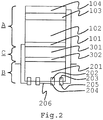
- FIG. 2 shows a conceptual diagram of a multi-junction solar cell in the form in which two photoelectric conversion devices for the second solar cell B are not isolated.
- the multi-junction solar cell in FIG. 2 has the first solar cell A, an insulating layer C, and the second solar cell B.
- the second solar cell B has two photoelectric conversion devices connected in series. Because the two photoelectric conversion devices are not isolated, a back electromotive force relative to the photoelectric conversion devices is generated between the two photoelectric conversion devices. Because the back electromotive force partially cancels out electricity generated by the photoelectric conversion devices, the second solar cell B is low in conversion efficiency, furthermore, voltage matching is not achieved well between the first solar cell A and the second solar cell B, and thus, the multi-junction solar cell is also low in conversion efficiency.
- FIG. 3 shows a conceptual diagram of a multi-junction solar cell in the form in which two photoelectric conversion devices for the second solar cell B are isolated.
- the multi-junction solar cell in FIG. 3 is adapted in the same fashion as the multi-junction solar cell in FIG. 2 , except for cutting between the second photoelectric conversion devices (for example, between devices 200A and 200B in FIG. 1 ) and the cut region filled with an insulator.
- the multi-junction solar cell in FIG. 3 has a device isolation region formed so as to achieve complete isolation between the photoelectric conversion devices of the second solar cell B, and thus generates no electromotive force between the photoelectric conversion devices.
- This form increases the open circuit voltage of the second solar cell B, and facilitates voltage matching between the first solar cell A and the second solar cell B.
- the second solar cell B from the perspective of positioning accuracy, it is preferable to attach the first solar cell A, the insulating layer C, and the second solar cell B before the device isolation.
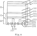
- FIG. 4 shows a conceptual diagram of a multi-junction solar cell in the form in which three photoelectric conversion devices 200 for the second solar cell B are isolated.
- the multi-junction solar cell in FIG. 4 has incomplete cutting between the second photoelectric conversion devices (for example, between the respective devices 200A to 200C in FIG. 1 ), and the cut regions filled with an insulator to isolate the second photoelectric conversion devices.
- the device isolations in the two regions differ in depth. While the device isolations preferably have the form of completely separating the silicon layers 201, voltage leakage between the second photoelectric conversion devices can be reduced even in the case of the incomplete separations.
- FIG. 4 shows a conceptual diagram of a multi-junction solar cell in the form in which three photoelectric conversion devices 200 for the second solar cell B are isolated.
- the multi-junction solar cell in FIG. 4 has incomplete cutting between the second photoelectric conversion devices (for example, between the respective devices 200A to 200C in FIG. 1 ), and the cut regions filled with an insulator to isolate the second photoelectric conversion devices
- the device isolation region on the left-hand side is deeper than that on the right-hand side, and the left region between the photoelectric conversion devices is thus more effective for reducing voltage/current leakage.
- This form increases the open circuit voltage of the second solar cell B, and facilitates voltage matching between the first solar cell A and the second solar cell B. It is also possible to adjust the open circuit voltage of the second solar cell B, depending on the depth of the device isolation. For the second solar cell B in this form, the device isolation is incompletely achieved, and it is thus also preferable to attach the first solar cell A, the insulating layer C, and the second solar cell B after the device isolation.
- FIG. 5 shows a conceptual diagram of a multi-junction solar cell in the form in which three photoelectric conversion devices for the second solar cell B are isolated, and a rectifying device (diode) is provided between a p electrode 204 and an n electrode 205 for each photoelectric conversion device .
- the multi-junction solar cell in FIG. 5 has the form of the three photoelectric conversion devices respectively provided with bypass diodes, unlike the multi-junction solar cell in FIG. 4 .
- the solar cell configured in this way is able to generate electricity as the second solar cell B, even when any of the photoelectric conversion devices is broken to turn into an insulated condition, because of the flow of electricity through the bypass diodes.
- FIG. 6 shows a conceptual diagram of a multi-junction solar cell in the form in which three photoelectric conversion devices for the second solar cell B are isolated by carrying out device isolation of making single-crystal silicon amorphous with the use of ion beams.
- the multi-junction solar cell in FIG. 6 has the form of mobility decreased by irradiating silicon layers between the photoelectric conversion devices with ion beams to make the silicon layers 201 between the photoelectric conversion devices amorphous, instead of insulating regions formed between the photoelectric conversion devices, unlike the multi-junction solar cell in FIG. 4 .
- the second solar cell B achieves on the order of 10% of current in the case of complete device isolation, but the conversion efficiency of the multi-junction solar cell can be increased as compared with the form without device isolation, because voltage matching can be achieved between the first solar cell A and the second solar cell B.
- an insulating film is preferably provided on the silicon layers 201 to reduce leakage.
- the insulating film is typically SiO 2 formed with the use of a mask.
- the wiring parts 206 connect the p electrodes 204 and n electrodes 205 of adjacent photoelectric conversion devices to connect the photoelectric conversion devices in series.
- a metal film such as, for example, Cu and Al can be thus used in the same manner as the p electrodes 204 and n electrodes 205.
- the series wiring and device isolation according to the embodiment can be applied for front contacts in the case of a multi-junction solar cell with the second solar cell B as a top cell.
- the second solar cell is adopted as a top cell, it is preferable to use a transparent member for the electrodes and wirings of the second solar cell B.
- the insulating layer C is an insulating layer for joining the first solar cell A and the second solar cell B.
- the insulating layer C is, for example, soda-lime glass, quartz, glass, a resin layer (including an adhesive layer), or a laminated body with the use of these members.
- the insulating layer C of the multi-junction solar cell in FIG. 1 includes blue sheet glass 301 and an acrylic resin adhesive layer 302.
- the insulating layer C connects the first solar cell A and the second solar cell B, and transmits light passing through the first solar cell A to guide the light to the second solar cell B.
- acrylic binders can be used as the adhesive.
- the device isolation regions 207 of the second solar cell B may be formed in the insulating layer C in some cases.
- a multi-junction solar cell according to an embodiment will be more specifically described below with reference to examples.
- Example 1 a multi-junction solar cell is prepared in the form shown in the conceptual diagram of FIG. 3 .
- a first solar cell is prepared on soda-lime glass to serve as a part of the insulating layer.
- soda-lime glass of 1 cm ⁇ 1 cm with an ITO film of 200 nm in thickness formed thereon
- a Cu 0.85 (In 0.12 Ga 0.59 Al 0.29 ) (S 0.1 Se 0.9 ) 2 thin film to serve as a photoelectric conversion layer is deposited by a deposition method (three-step method).
- the substrate temperature is increased to 300°C, and Al, In, Ga, S, and Se are deposited (first step).
- the substrate temperature is increased to 500°C, and Cu, S, and Se are deposited.
- the initiation of an endothermic reaction is confirmed, and the deposition of Cu is stopped once on reaching a composition with excessive Cu (second step).
- Al, In, Ga, S, and Se are again deposited (third step) to provide a composition with slightly excessive Group IIIb element such as Al, In, or Ga.
- the photoelectric conversion layer has a film thickness on the order of approximately 2000 nm.
- the member after the deposition of the photoelectric conversion layer is immersed in a 25% ammonia solution with 0.08 mM cadmium sulfate dissolved therein, and reacted at room temperature (25°C) for 22 minutes.
- an n-type semiconductor layer doped with Cd is formed in a region of the photoelectric conversion layer on the order of 100 nm in depth on the side on which an upper electrode is to be formed.
- a CdS contact layer and an i-ZnO thin film as a semi-insulating layer are deposited by spin coating.
- deposition on the order of 300 nm is carried out by sputtering with the use of a ZnO : Al target containing 2 wt% of alumina (Al 2 O 3 ) to serve as an upper electrode.
- MgF 2 on the order of 105 nm is deposited by an electron beam evaporation method to prepare the first solar cell on the soda-lime glass.
- a second solar cell is prepared.
- One surface of an n-type single-crystal silicon layer of 200 ⁇ m in thickness is partially made p+ type and n+ type by partial ion implantation with a B element and a P element respectively into separate regions so as to have a concentration of 2.0 ⁇ 10 -19 cm -3 , a depth of 0.2 ⁇ m, and a width of 300 ⁇ m.
- the p+ type and n+ type are imparted to form two p+ regions and two n+ regions in the order of p+, n+, p+, and n+ at the back contact side of the silicon layer.
- two photoelectric conversion devices are formed.
- the surface of the silicon layer of the second solar cell which is opposite to the surface with the n+ regions and p+ regions, is joined to the surface of the soda-lime glass with the first solar cell, which is opposite to the surface with the first solar cell.
- the adhesive layer has a thickness on the order of 50 ⁇ m.
- a region between the two photoelectric conversion devices is cut with the use of a dicer in a direction from the back contact side of the silicon layer to the first solar cell over the silicon layer length of 1 cm from end to end to isolate the photoelectric conversion devices of the silicon layer.
- the cutting depth is 200 ⁇ m, which is equal to the thickness of the silicon layer, and the cutting width is 15 ⁇ m.
- the gap produced by cutting the silicon layer is filled with an acrylic resin.
- the ITO electrode, upper electrode, p+ region, and n+ region of the first solar cell are connected to a semiconductor parameter analyzer to measure each of the open circuit voltage (Voc), short-circuit current density (Jsc), and conversion efficiency ( ⁇ ) for the first solar cell alone, the second solar cell alone with the first solar cell formed, and further the multi-junction solar cell of the first solar cell and second solar cell connected in parallel under quasi-sunlight irradiation of AM1. 5 through a solar simulator.
- the measured results are shown in Table 1.
- a multi-junction solar cell is prepared in the same way as in Example 1.
- the open circuit voltage, short-circuit current density, and conversion efficiency are also measured in the same way as in Example 1. The measured results are shown in Table 1.
- a multi-junction solar cell is prepared in the same way as in Example 1.
- the open circuit voltage, short-circuit current density, and conversion efficiency are also measured in the same way as in Example 1. The measured results are shown in Table 1.
- a multi-junction solar cell is prepared in the same way as in Example 1.
- the length of the region with the silicon layer left without being cut accounts for 10% in total, i.e., 5% of the cutting length in Example 1 for each of the two regions.
- the open circuit voltage, short-circuit current density, and conversion efficiency are also measured in the same way as in Example 1. The measured results are shown in Table 1.
- Example 1 Except that the device isolation is not carried out, a multi-junction solar cell is prepared in the same way as in Example 1. On the multi-junction solar cell according to Comparative Example 1, the open circuit voltage, short-circuit current density, and conversion efficiency are also measured in the same way as in Example 1. The measured results are shown in Table 1.
- Example 1 indicates intended performance of an almost twofold increase in the voltage of the second solar cell and a decrease in current value to almost one-half, with respect to the voltage a cell without serial connection. It can be understood that Example 2 causes losses in both voltage and current, due to the presence of the leakage component. It can be understood that incomplete device isolation interferes with the improvement in efficiency in Example 3. Examples 4 and 5 have current values slightly increased as compared with Example 1. This is believed to be due to the fact that light that is not absorbed by the cut section is diffusely reflected and absorbed by the surrounding cell.
- the cut section formed in the adhesive may deviate from the cut section of the underlayer solar cell in some cases, but the increase in current can be expected as long as the sections are partially overlapped.
- the form is considered effective as long as the portion is not a significant source of leakage. (for example, when the cutting depth is 90% only at a point of the cut section)
- Comparative Example 1 has achieved almost no improvement in the voltage of the second solar cell. This is due to the fact that any series structure is not achieved because of carrying out no device isolation. Because the shape of the lower electrode differs in pattern from the shape without series connection, some of photons absorbed are recombined to also fail to earn the current value, thereby resulting in the low efficiency. When the results are compared between each example and Comparative Example 1, it can be understood that voltage matching is unable to be achieved without device isolation, and halfway device isolation is unlikely to achieve the effect of increasing the efficiency, due to the leakage component.
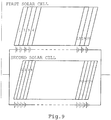
- FIG. 9 shows a conceptual diagram of and a circuit of the prepared multi-junction solar cell.
- the numerical numbers in FIG. 9 refers to numbers for the photoelectric conversion devices.
- a photoelectric conversion layer is formed which is divided into twenty equal parts by scribing. Thereafter, an upper electrode is formed so as to connect ten photoelectric conversion devices in series, i.e., photoelectric conversion devices 1 to 10 in series and photoelectric conversion devices 11 to 20 in series. In this case, the photoelectric conversion devices 10 and 11 are not connected in series or in parallel. Furthermore, an anti-reflection film is formed. The two sets of ten photoelectric conversion devices connected in series are connected in parallel to prepare the first solar cell.
- FIG. 10 shows a conceptual diagram of and a circuit of the prepared multi-junction solar cell.
- the open circuit voltage, short-circuit current density, and conversion efficiency are also measured in the same way as in Example 1. The measured results are shown in Table 2.
- an ITO electrode is divided by scribing into parts for twenty devices, and a photoelectric conversion layer is deposited on the ITO electrode.
- the photoelectric conversion layer is subjected to scribing so as to be divided into twenty equal parts for photoelectric conversion devices, an upper electrode is formed so as to connect the twenty photoelectric conversion devices in series, and an anti-reflection film is further formed to prepare the first solar cell with the twenty photoelectric conversion devices connected in series.
- a silicon layer of 12 cm ⁇ 5.5 cm is subjected to ion implantation to form nineteen regions for each of p+ and n+.
- the silicon layer subjected to the ion implantation is bonded to the substrate with the first solar cell formed.
- FIG. 11 shows a conceptual diagram of and a circuit of the prepared multi-junction solar cell.
- the open circuit voltage, short-circuit current density, and conversion efficiency are also measured in the same way as in Example 1. The measured results are shown in Table 2.
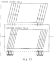
- Example 9 provides a multi-junction solar cell where the second photoelectric conversion devices according to Example 6 are provided with bypass diodes. Cathodes of the diodes are connected to p electrodes of the second photoelectric conversion devices, whereas anodes thereof are connected to n electrodes of the second photoelectric conversion devices.
- the bypass diodes are diodes externally attached, rather than formed in the silicon layers of the second photoelectric conversion devices.
- FIG. 12 shows a conceptual diagram of the prepared multi-junction solar cell according to Example 9. On the prepared multi-junction solar cell, the open circuit voltage, short-circuit current density, and conversion efficiency are measured in the same way as in Example 1. The measured results are shown in Table 2.
- FIG. 13 shows a conceptual diagram of and a circuit of the prepared multi-junction solar cell.
- the blacked region with a white letter refers to a region without any photoelectric conversion device.
- the open circuit voltage, short-circuit current density, and conversion efficiency are measured in the same way as in Example 1. The measured results are shown in Table 2.
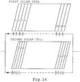
- Example 10 provides a multi-junction solar cell where the first solar cell and second solar cell according to Example 6 are each connected in series with a diode.
- FIG. 14 shows a conceptual diagram of and a circuit of the prepared multi-junction solar cell according to Example 10.
- the open circuit voltage, short-circuit current density, and conversion efficiency are measured in the same way as in Example 1. The measured results are shown in Table 2.
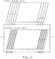
- Example 11 except that an acrylic resin is poured into grooves formed through the device isolation by cutting with a dicer in the preparation of the thirty-eight second photoelectric conversion devices which are equal in area to each other in Example 6, a multi-junction solar cell is prepared in the same way as in Example 6.
- FIG. 15 shows a conceptual diagram of and a circuit of the prepared multi-junction solar cell according to Example 11.
- the open circuit voltage, short-circuit current density, and conversion efficiency are also measured in the same way as in Example 1. The measured results are shown in Table 2.
- Example 6 achieves, due to the increased number of series connections and a reduced voltage difference between the first and second solar cells, a higher efficiency solar cell than Examples 1 to 5, which shows effectiveness.
- Example 7 it can be understood that it is possible to reduce the number of cuts in the lower single-crystal silicon solar cell by lowering the open circuit voltage with the parallel-connected upper solar cell. This means that dead area near the cut sections can be reduced so that it is possible to improve the efficiency.
- the number of parallel connections can be selected freely, which thus becomes an important approach for the increase in efficiency in the creation of large panels. From Example 8, it can be understood that it is possible to prepare respective wafers and connect the wafers in series in the creation of solar cell panels.
- Example 13 except for the use of CuAl 0.59 Ga 0.41 Se 2 for the p layers in the photoelectric conversion layer of the first solar cell in Example 6 and the change of the division number by scribing from 38 to 46, a multi-junction solar cell is prepared in the same way as in Example 6. On the multi-junction solar cell according to Example 13, the open circuit voltage, short-circuit current density, and conversion efficiency are also measured in the same way as in Example 1. The measured results are shown in Table 3.
- Example 12 produces almost no change in the bandgap of the first solar cell, and thus shows almost no difference from Example 6.
- Example 13 produces a substantial change in the bandgap of the first solar cell, and thus undergoes a change in the amount of light absorbed by the second solar cell, while Example 13 improves the efficiency with the configuration.
- Comparative Examples 3 and 4 fail to achieve the effect of the multi-junction configuration of the first and second solar cells, and adversely undergo characteristic degradation. The loss is believed to be increased because of substantial differences in both voltage and current. From Comparative Examples 3 and 4, it can be understood that the multi-junction effect with the first solar cell is not achieved, unless series connections are made in the second solar cell.
- the advantageous effect of the present disclosure can be expected even when Cu(In,Al)Se 2 or Cu(Ga,Al)Se 2 is used for the p layers of the first solar cell. From the foregoing, it can be understood that a similar effect will be achieved even in the case of Cu(In,Al) (S,Se) 2 or Cu(Ga,Al) (S,Se) 2 , besides the examples previously described. Furthermore, a similar effect can be expected even in the case of Ag(In,Ga,Al) (S,Se) 2 with Ag in place of Cu.
Landscapes
- Photovoltaic Devices (AREA)
- Life Sciences & Earth Sciences (AREA)
- Engineering & Computer Science (AREA)
- Sustainable Development (AREA)
- Sustainable Energy (AREA)
Claims (10)
- Solarzelle mit mehreren Anschlüssen, umfassend:eine erste Solarzelle (A), die eine erste photoelektrische Umwandlungsvorrichtung (100) umfasst;eine zweite Solarzelle (B), die eine Vielzahl von in Reihe geschalteten zweiten photoelektrischen Umwandlungsvorrichtungen (200) umfasst, wobei jede der zweiten photoelektrischen Umwandlungsvorrichtungen (200) eine n-Typ- oder eine p-Typ-Siliziumschicht (201) und Rückseitenkontakte (204, 205) aufweist; undeine Isolierschicht (C) zwischen der ersten Solarzelle (A) und der zweiten Solarzelle (B),wobei jede aus der Vielzahl der zweiten photoelektrischen Umwandlungsvorrichtungen (200) sowohl einen n+-Bereich (203), der an der der Isolierschicht (C) gegenüberliegenden Oberfläche der Siliziumschicht (201) freiliegt, als auch einen p+-Bereich (202) aufweist, der an der der Isolierschicht (C) gegenüberliegenden Oberfläche der Siliziumschicht (201) freiliegt, wobei die Rückseitenkontakte (204, 205) mit den Bereichen (202, 203) verbunden sind,wobei zwischen den in Reihe geschalteten zweiten photoelektrischen Umwandlungsvorrichtungen (200) Vorrichtungsisolierbereiche (207) bereitgestellt sind, unddie Vorrichtungsisolierbereiche (207) in einem Teil der Isolierschicht (C) vorhanden sind.
- Solarzelle nach Anspruch 1, wobei der Vorrichtungsisolierbereich (207) ein Bereich ist, der durch Isolieren von 40% oder mehr einer Querschnittsfläche zwischen den zweiten photoelektrischen Umwandlungsvorrichtungen (200) erhalten wird, wobei die Querschnittsfläche die zweiten photoelektrischen Umwandlungsvorrichtungen (200) in Reihe schaltet.
- Solarzelle nach einem der vorstehenden Ansprüche, wobei die erste photoelektrische Umwandlungsvorrichtung (100) eine photoelektrische Umwandlungsschicht (102) umfasst, die eines aus einem Verbindungshalbleiter vom Chalkopyrit-Typ, einem Verbindungshalbleiter vom Stannit-Typ und einem Verbindungshalbleiter vom Kesterit-Typ enthält.
- Solarzelle nach einem der vorstehenden Ansprüche, wobei die zweiten photoelektrischen Umwandlungsvorrichtungen (200) eine photoelektrische Umwandlungsschicht (201) umfassen, die einkristallines Silizium enthält.
- Solarzelle nach einem der vorstehenden Ansprüche, wobei der Vorrichtungsisolierbereich (207) ein amorpher Bereich ist, der 40 % oder mehr einer Querschnittsfläche zwischen den zweiten photoelektrischen Umwandlungsvorrichtungen (200) ausmacht, wobei die Querschnittsfläche die zweiten photoelektrischen Umwandlungsvorrichtungen (200) in Reihe schaltet.
- Solarzelle nach einem der vorstehenden Ansprüche, weiter eine Gleichrichtervorrichtung umfassend, die mit mindestens einem aus der ersten photoelektrischen Umwandlungsvorrichtung (100) und den zweiten photoelektrischen Umwandlungsvorrichtungen (200) parallelgeschaltet ist.
- Solarzelle nach einem der vorstehenden Ansprüche, weiter eine Gleichrichtervorrichtung umfassend, die mit mindestens einer aus der ersten Solarzelle (A) und der zweiten Solarzelle (B) in Reihe geschaltet ist.
- Solarzelle nach einem der vorstehenden Ansprüche, wobei die erste Solarzelle (A) und die zweite Solarzelle (B) parallelgeschaltet sind.
- Solarzelle nach einem der vorstehenden Ansprüche, wobei jede der zweiten photoelektrischen Umwandlungsvorrichtungen (200) eine p-Typ-Elektrode (204) und eine n-Typ-Elektrode (205) aufweist, und
die p-Typ-Elektrode (204) und die n-Typ-Elektrode (205) jeder der zweiten photoelektrischen Umwandlungsvorrichtungen (200) auf der Rückseitenkontaktfläche liegen, die der Isolierschicht gegenüberliegt. - Solarzelle nach Anspruch 9, wobei die p-Typ-Elektrode (204) einer zweiten photoelektrischen Umwandlungsvorrichtung (200) mit der n-Typ-Elektrode (205) einer anderen zweiten photoelektrischen Umwandlungsvorrichtung (200) verbunden ist, die an die eine zweite photoelektrische Umwandlungsvorrichtung (200) angrenzt.
Applications Claiming Priority (1)
| Application Number | Priority Date | Filing Date | Title |
|---|---|---|---|
| JP2013197610A JP6366914B2 (ja) | 2013-09-24 | 2013-09-24 | 多接合型太陽電池 |
Publications (3)
| Publication Number | Publication Date |
|---|---|
| EP2851965A2 EP2851965A2 (de) | 2015-03-25 |
| EP2851965A3 EP2851965A3 (de) | 2015-06-03 |
| EP2851965B1 true EP2851965B1 (de) | 2020-03-25 |
Family
ID=51421950
Family Applications (1)
| Application Number | Title | Priority Date | Filing Date |
|---|---|---|---|
| EP14182810.3A Active EP2851965B1 (de) | 2013-09-24 | 2014-08-29 | Solarzellen mit mehreren Anschlüssen |
Country Status (5)
| Country | Link |
|---|---|
| US (2) | US20150083186A1 (de) |
| EP (1) | EP2851965B1 (de) |
| JP (1) | JP6366914B2 (de) |
| CN (1) | CN104465845A (de) |
| TW (1) | TW201533924A (de) |
Families Citing this family (8)
| Publication number | Priority date | Publication date | Assignee | Title |
|---|---|---|---|---|
| TWI538230B (zh) * | 2015-03-23 | 2016-06-11 | 茂迪股份有限公司 | 背接觸太陽能電池組及其製造方法 |
| JP6829673B2 (ja) | 2017-09-19 | 2021-02-10 | 株式会社東芝 | 太陽電池システム及び太陽電池システムの制御方法 |
| WO2019180854A1 (ja) * | 2018-03-20 | 2019-09-26 | 株式会社 東芝 | 多接合型太陽電池モジュール及び太陽光発電システム |
| US11145774B2 (en) | 2018-05-30 | 2021-10-12 | Solar Inventions Llc | Configurable solar cells |
| US20240266454A1 (en) * | 2018-12-27 | 2024-08-08 | Solarpaint Ltd. | Flexible and Rollable Self-Floating and Self-Buoyant Solar Panels and Photovoltaic Devices |
| KR102224624B1 (ko) * | 2019-02-27 | 2021-03-08 | 한국과학기술연구원 | 다중접합 태양전지 및 이의 제조방법 |
| US10899728B2 (en) * | 2019-04-01 | 2021-01-26 | Delta Separations, Llc | System, method and apparatus for cannabinoid mixture separation and solvent recovery |
| US11107942B2 (en) * | 2019-04-30 | 2021-08-31 | Utica Leaseco, Llc | Sputtered then evaporated back metal process for increased throughput |
Citations (1)
| Publication number | Priority date | Publication date | Assignee | Title |
|---|---|---|---|---|
| US4295002A (en) * | 1980-06-23 | 1981-10-13 | International Business Machines Corporation | Heterojunction V-groove multijunction solar cell |
Family Cites Families (45)
| Publication number | Priority date | Publication date | Assignee | Title |
|---|---|---|---|---|
| US4110122A (en) * | 1976-05-26 | 1978-08-29 | Massachusetts Institute Of Technology | High-intensity, solid-state-solar cell device |
| US4200472A (en) * | 1978-06-05 | 1980-04-29 | The Regents Of The University Of California | Solar power system and high efficiency photovoltaic cells used therein |
| DE3135591A1 (de) * | 1981-09-09 | 1983-04-21 | Bogner, Udo, Dr., 8400 Regensburg | Spannungsabhaengiges optisches bauelement, insbesondere mit der funktion eines spannungsmemory und zur verbindung bzw. kopplung von elektrischen und/oder elektronischen teilen von anlagen miteinander |
| US4477721A (en) * | 1982-01-22 | 1984-10-16 | International Business Machines Corporation | Electro-optic signal conversion |
| US4461922A (en) * | 1983-02-14 | 1984-07-24 | Atlantic Richfield Company | Solar cell module |
| JPS6175567A (ja) | 1984-09-20 | 1986-04-17 | Sanyo Electric Co Ltd | 光起電力装置 |
| US5164019A (en) * | 1991-07-31 | 1992-11-17 | Sunpower Corporation | Monolithic series-connected solar cells having improved cell isolation and method of making same |
| US6166320A (en) * | 1998-03-19 | 2000-12-26 | Toyota Jidosha Kabushiki Kaisha | Tandem solar cell |
| JP4502445B2 (ja) * | 2000-03-16 | 2010-07-14 | 大日本印刷株式会社 | 反射防止フィルムの製造方法 |
| US7095050B2 (en) | 2002-02-28 | 2006-08-22 | Midwest Research Institute | Voltage-matched, monolithic, multi-band-gap devices |
| US20060162768A1 (en) * | 2002-05-21 | 2006-07-27 | Wanlass Mark W | Low bandgap, monolithic, multi-bandgap, optoelectronic devices |
| US20050150542A1 (en) | 2004-01-13 | 2005-07-14 | Arun Madan | Stable Three-Terminal and Four-Terminal Solar Cells and Solar Cell Panels Using Thin-Film Silicon Technology |
| JP4754801B2 (ja) | 2004-10-13 | 2011-08-24 | 浜松ホトニクス株式会社 | レーザ加工方法 |
| JP4703274B2 (ja) * | 2005-06-08 | 2011-06-15 | シャープ株式会社 | 太陽電池および太陽電池の製造方法 |
| JP4809632B2 (ja) | 2005-06-01 | 2011-11-09 | ルネサスエレクトロニクス株式会社 | 半導体装置の製造方法 |
| GB0519599D0 (en) * | 2005-09-26 | 2005-11-02 | Imp College Innovations Ltd | Photovoltaic cells |
| KR20070101917A (ko) | 2006-04-12 | 2007-10-18 | 엘지전자 주식회사 | 박막형 태양전지와 그의 제조방법 |
| KR20080079058A (ko) * | 2007-02-26 | 2008-08-29 | 엘지전자 주식회사 | 박막형 태양전지 모듈과 그의 제조방법 |
| JP2011526737A (ja) | 2008-07-03 | 2011-10-13 | アイメック | 多重接合太陽電池モジュールおよびそのプロセス |
| KR20100028729A (ko) * | 2008-09-05 | 2010-03-15 | 삼성전자주식회사 | 복층 구조의 태양 전지 및 그 제조 방법 |
| US8138410B2 (en) | 2008-10-01 | 2012-03-20 | International Business Machines Corporation | Optical tandem photovoltaic cell panels |
| US8835748B2 (en) * | 2009-01-06 | 2014-09-16 | Sunlight Photonics Inc. | Multi-junction PV module |
| WO2010087312A1 (ja) * | 2009-01-28 | 2010-08-05 | 三菱電機株式会社 | 薄膜光電変換装置およびその製造方法 |
| IT1392995B1 (it) * | 2009-02-12 | 2012-04-02 | St Microelectronics Srl | Pannello solare con due moduli fotovoltaici multicellulari monolitici di diversa tecnologia |
| JP5379845B2 (ja) | 2009-03-02 | 2013-12-25 | 株式会社カネカ | 薄膜太陽電池モジュール |
| CN102356470B (zh) * | 2009-03-18 | 2014-07-02 | 三菱电机株式会社 | 光电转换装置 |
| US20100263713A1 (en) * | 2009-04-16 | 2010-10-21 | Solfocus, Inc. | Four Terminal Monolithic Multijunction Solar Cell |
| CN102460721B (zh) * | 2009-06-05 | 2015-07-01 | 株式会社半导体能源研究所 | 光电转换装置及其制造方法 |
| WO2010140539A1 (en) * | 2009-06-05 | 2010-12-09 | Semiconductor Energy Laboratory Co., Ltd. | Photoelectric conversion device and method for manufacturing the same |
| CN101924156A (zh) * | 2009-06-11 | 2010-12-22 | 亚洲太阳科技有限公司 | 复合式串联或并联的薄膜太阳能电池及其制作方法 |
| US20110088744A1 (en) | 2009-10-21 | 2011-04-21 | Bp Corporation North America Inc. | Photovoltaic Module Failure Detection Devices and Methods |
| US20110155230A1 (en) * | 2009-12-28 | 2011-06-30 | Du Pont Apollo Limited | Multi-bandgap solar cell and method producing the same |
| NL2004065C2 (en) * | 2010-01-06 | 2011-07-07 | Stichting Energie | Solar panel module and method for manufacturing such a solar panel module. |
| US8704083B2 (en) * | 2010-02-11 | 2014-04-22 | Semiconductor Energy Laboratory Co., Ltd. | Photoelectric conversion device and fabrication method thereof |
| EP2556542A1 (de) * | 2010-04-09 | 2013-02-13 | Platzer-Björkman, Charlotte | Photovoltaische dünnschichtsolarzellen |
| US20120204939A1 (en) * | 2010-08-23 | 2012-08-16 | Stion Corporation | Structure and Method for High Efficiency CIS/CIGS-based Tandem Photovoltaic Module |
| US8409906B2 (en) * | 2010-10-25 | 2013-04-02 | Imra America, Inc. | Non-vacuum method for fabrication of a photovoltaic absorber layer |
| JP2012138556A (ja) | 2010-12-27 | 2012-07-19 | Fumimasa Yo | 多接合型太陽電池 |
| US20120180854A1 (en) * | 2011-01-18 | 2012-07-19 | Bellanger Mathieu | Mechanical stacking structure for multi-junction photovoltaic devices and method of making |
| JP2012195416A (ja) | 2011-03-16 | 2012-10-11 | Fujifilm Corp | 光電変換素子の製造方法 |
| KR20120111657A (ko) | 2011-04-01 | 2012-10-10 | 삼성전자주식회사 | 태양 전지 |
| US8530263B2 (en) | 2011-08-10 | 2013-09-10 | Taiwan Semiconductor Manufacturing Co., Ltd. | Superstrate solar cell |
| CN102956650A (zh) * | 2011-08-26 | 2013-03-06 | 刘莹 | 一种新型叠层薄膜太阳能电池 |
| US20150340528A1 (en) * | 2012-12-10 | 2015-11-26 | Alliance For Sustainable Energy, Llc | Monolithic tandem voltage-matched multijuntion solar cells |
| JP5708695B2 (ja) * | 2013-04-12 | 2015-04-30 | トヨタ自動車株式会社 | 太陽電池セル |
-
2013
- 2013-09-24 JP JP2013197610A patent/JP6366914B2/ja active Active
-
2014
- 2014-08-20 TW TW103128641A patent/TW201533924A/zh unknown
- 2014-08-29 EP EP14182810.3A patent/EP2851965B1/de active Active
- 2014-09-01 CN CN201410440200.9A patent/CN104465845A/zh active Pending
- 2014-09-05 US US14/478,252 patent/US20150083186A1/en not_active Abandoned
-
2018
- 2018-01-23 US US15/878,000 patent/US11398577B2/en active Active
Patent Citations (1)
| Publication number | Priority date | Publication date | Assignee | Title |
|---|---|---|---|---|
| US4295002A (en) * | 1980-06-23 | 1981-10-13 | International Business Machines Corporation | Heterojunction V-groove multijunction solar cell |
Also Published As
| Publication number | Publication date |
|---|---|
| JP2015065249A (ja) | 2015-04-09 |
| US11398577B2 (en) | 2022-07-26 |
| EP2851965A3 (de) | 2015-06-03 |
| US20150083186A1 (en) | 2015-03-26 |
| US20180151771A1 (en) | 2018-05-31 |
| EP2851965A2 (de) | 2015-03-25 |
| JP6366914B2 (ja) | 2018-08-01 |
| CN104465845A (zh) | 2015-03-25 |
| TW201533924A (zh) | 2015-09-01 |
Similar Documents
| Publication | Publication Date | Title |
|---|---|---|
| EP2851965B1 (de) | Solarzellen mit mehreren Anschlüssen | |
| US11205732B2 (en) | Multi-junction solar cell | |
| US8916767B2 (en) | Solar cell and method of fabricating the same | |
| US8658890B2 (en) | Solar cell and method of manufacturing solar cell | |
| US20130206219A1 (en) | Cooperative photovoltaic networks and photovoltaic cell adaptations for use therein | |
| JP5901773B2 (ja) | 直列接続部を含む薄膜ソーラーモジュール、及び、複数の薄膜ソーラーセルを直列接続する方法 | |
| US20120186643A1 (en) | Compound semiconductor solar cells and methods of fabricating the same | |
| US9935211B2 (en) | Back contact structure for photovoltaic devices such as copper-indium-diselenide solar cells | |
| EP2485272A2 (de) | Vorrichtung zur solarstromerzeugung sowie verfahren zu ihrer herstellung | |
| US20170243999A1 (en) | Solar cell | |
| US20110214708A1 (en) | Solar cell module and solar cell device | |
| CN102576758A (zh) | 太阳能电池设备及其制造方法 | |
| EP2768030A2 (de) | Solarzelle und Verfahren zu ihrer Herstellung | |
| KR101114169B1 (ko) | 태양광 발전장치 | |
| KR101428146B1 (ko) | 태양전지 모듈 및 이의 제조방법 | |
| JP2011077149A (ja) | 太陽電池モジュール | |
| CN103718307A (zh) | 具有减小的功率损耗的太阳能模块及其制造方法 | |
| JP6133691B2 (ja) | 太陽電池 | |
| US20170077327A1 (en) | Photoelectric conversion element, solar cell, solar cell module, and solar power generating system | |
| Prathapani et al. | A comprehensive perspective on the fabrication of CuGaSe2/Si tandem solar cells | |
| KR20130086003A (ko) | 태양전지 및 그 제조 방법 | |
| WO2012153640A1 (ja) | 光電変換素子および太陽電池 | |
| KR101162162B1 (ko) | 태양전지용 전극 페이스트, 이를 이용한 태양전지, 및 태양전지의 제조방법 | |
| KR20110045181A (ko) | 태양전지 및 이의 제조방법 | |
| KR20150109223A (ko) | 태양 전지 및 그 제조 방법 |
Legal Events
| Date | Code | Title | Description |
|---|---|---|---|
| PUAI | Public reference made under article 153(3) epc to a published international application that has entered the european phase |
Free format text: ORIGINAL CODE: 0009012 |
|
| 17P | Request for examination filed |
Effective date: 20140829 |
|
| AK | Designated contracting states |
Kind code of ref document: A2 Designated state(s): AL AT BE BG CH CY CZ DE DK EE ES FI FR GB GR HR HU IE IS IT LI LT LU LV MC MK MT NL NO PL PT RO RS SE SI SK SM TR |
|
| AX | Request for extension of the european patent |
Extension state: BA ME |
|
| REG | Reference to a national code |
Ref country code: DE Ref legal event code: R079 Ref document number: 602014062760 Country of ref document: DE Free format text: PREVIOUS MAIN CLASS: H01L0031068700 Ipc: H01L0031043000 |
|
| PUAL | Search report despatched |
Free format text: ORIGINAL CODE: 0009013 |
|
| AK | Designated contracting states |
Kind code of ref document: A3 Designated state(s): AL AT BE BG CH CY CZ DE DK EE ES FI FR GB GR HR HU IE IS IT LI LT LU LV MC MK MT NL NO PL PT RO RS SE SI SK SM TR |
|
| AX | Request for extension of the european patent |
Extension state: BA ME |
|
| RIC1 | Information provided on ipc code assigned before grant |
Ipc: H01L 31/043 20140101AFI20150428BHEP |
|
| STAA | Information on the status of an ep patent application or granted ep patent |
Free format text: STATUS: EXAMINATION IS IN PROGRESS |
|
| 17Q | First examination report despatched |
Effective date: 20190510 |
|
| GRAP | Despatch of communication of intention to grant a patent |
Free format text: ORIGINAL CODE: EPIDOSNIGR1 |
|
| STAA | Information on the status of an ep patent application or granted ep patent |
Free format text: STATUS: GRANT OF PATENT IS INTENDED |
|
| INTG | Intention to grant announced |
Effective date: 20191129 |
|
| GRAS | Grant fee paid |
Free format text: ORIGINAL CODE: EPIDOSNIGR3 |
|
| GRAA | (expected) grant |
Free format text: ORIGINAL CODE: 0009210 |
|
| STAA | Information on the status of an ep patent application or granted ep patent |
Free format text: STATUS: THE PATENT HAS BEEN GRANTED |
|
| AK | Designated contracting states |
Kind code of ref document: B1 Designated state(s): AL AT BE BG CH CY CZ DE DK EE ES FI FR GB GR HR HU IE IS IT LI LT LU LV MC MK MT NL NO PL PT RO RS SE SI SK SM TR |
|
| REG | Reference to a national code |
Ref country code: GB Ref legal event code: FG4D |
|
| REG | Reference to a national code |
Ref country code: AT Ref legal event code: REF Ref document number: 1249589 Country of ref document: AT Kind code of ref document: T Effective date: 20200415 Ref country code: IE Ref legal event code: FG4D |
|
| REG | Reference to a national code |
Ref country code: DE Ref legal event code: R096 Ref document number: 602014062760 Country of ref document: DE |
|
| PG25 | Lapsed in a contracting state [announced via postgrant information from national office to epo] |
Ref country code: RS Free format text: LAPSE BECAUSE OF FAILURE TO SUBMIT A TRANSLATION OF THE DESCRIPTION OR TO PAY THE FEE WITHIN THE PRESCRIBED TIME-LIMIT Effective date: 20200325 Ref country code: FI Free format text: LAPSE BECAUSE OF FAILURE TO SUBMIT A TRANSLATION OF THE DESCRIPTION OR TO PAY THE FEE WITHIN THE PRESCRIBED TIME-LIMIT Effective date: 20200325 Ref country code: NO Free format text: LAPSE BECAUSE OF FAILURE TO SUBMIT A TRANSLATION OF THE DESCRIPTION OR TO PAY THE FEE WITHIN THE PRESCRIBED TIME-LIMIT Effective date: 20200625 |
|
| PG25 | Lapsed in a contracting state [announced via postgrant information from national office to epo] |
Ref country code: BG Free format text: LAPSE BECAUSE OF FAILURE TO SUBMIT A TRANSLATION OF THE DESCRIPTION OR TO PAY THE FEE WITHIN THE PRESCRIBED TIME-LIMIT Effective date: 20200625 Ref country code: HR Free format text: LAPSE BECAUSE OF FAILURE TO SUBMIT A TRANSLATION OF THE DESCRIPTION OR TO PAY THE FEE WITHIN THE PRESCRIBED TIME-LIMIT Effective date: 20200325 Ref country code: GR Free format text: LAPSE BECAUSE OF FAILURE TO SUBMIT A TRANSLATION OF THE DESCRIPTION OR TO PAY THE FEE WITHIN THE PRESCRIBED TIME-LIMIT Effective date: 20200626 Ref country code: LV Free format text: LAPSE BECAUSE OF FAILURE TO SUBMIT A TRANSLATION OF THE DESCRIPTION OR TO PAY THE FEE WITHIN THE PRESCRIBED TIME-LIMIT Effective date: 20200325 Ref country code: SE Free format text: LAPSE BECAUSE OF FAILURE TO SUBMIT A TRANSLATION OF THE DESCRIPTION OR TO PAY THE FEE WITHIN THE PRESCRIBED TIME-LIMIT Effective date: 20200325 |
|
| REG | Reference to a national code |
Ref country code: NL Ref legal event code: MP Effective date: 20200325 |
|
| REG | Reference to a national code |
Ref country code: LT Ref legal event code: MG4D |
|
| PG25 | Lapsed in a contracting state [announced via postgrant information from national office to epo] |
Ref country code: NL Free format text: LAPSE BECAUSE OF FAILURE TO SUBMIT A TRANSLATION OF THE DESCRIPTION OR TO PAY THE FEE WITHIN THE PRESCRIBED TIME-LIMIT Effective date: 20200325 |
|
| PG25 | Lapsed in a contracting state [announced via postgrant information from national office to epo] |
Ref country code: PT Free format text: LAPSE BECAUSE OF FAILURE TO SUBMIT A TRANSLATION OF THE DESCRIPTION OR TO PAY THE FEE WITHIN THE PRESCRIBED TIME-LIMIT Effective date: 20200818 Ref country code: EE Free format text: LAPSE BECAUSE OF FAILURE TO SUBMIT A TRANSLATION OF THE DESCRIPTION OR TO PAY THE FEE WITHIN THE PRESCRIBED TIME-LIMIT Effective date: 20200325 Ref country code: SM Free format text: LAPSE BECAUSE OF FAILURE TO SUBMIT A TRANSLATION OF THE DESCRIPTION OR TO PAY THE FEE WITHIN THE PRESCRIBED TIME-LIMIT Effective date: 20200325 Ref country code: RO Free format text: LAPSE BECAUSE OF FAILURE TO SUBMIT A TRANSLATION OF THE DESCRIPTION OR TO PAY THE FEE WITHIN THE PRESCRIBED TIME-LIMIT Effective date: 20200325 Ref country code: IS Free format text: LAPSE BECAUSE OF FAILURE TO SUBMIT A TRANSLATION OF THE DESCRIPTION OR TO PAY THE FEE WITHIN THE PRESCRIBED TIME-LIMIT Effective date: 20200725 Ref country code: SK Free format text: LAPSE BECAUSE OF FAILURE TO SUBMIT A TRANSLATION OF THE DESCRIPTION OR TO PAY THE FEE WITHIN THE PRESCRIBED TIME-LIMIT Effective date: 20200325 Ref country code: CZ Free format text: LAPSE BECAUSE OF FAILURE TO SUBMIT A TRANSLATION OF THE DESCRIPTION OR TO PAY THE FEE WITHIN THE PRESCRIBED TIME-LIMIT Effective date: 20200325 Ref country code: LT Free format text: LAPSE BECAUSE OF FAILURE TO SUBMIT A TRANSLATION OF THE DESCRIPTION OR TO PAY THE FEE WITHIN THE PRESCRIBED TIME-LIMIT Effective date: 20200325 |
|
| REG | Reference to a national code |
Ref country code: AT Ref legal event code: MK05 Ref document number: 1249589 Country of ref document: AT Kind code of ref document: T Effective date: 20200325 |
|
| REG | Reference to a national code |
Ref country code: DE Ref legal event code: R097 Ref document number: 602014062760 Country of ref document: DE |
|
| PG25 | Lapsed in a contracting state [announced via postgrant information from national office to epo] |
Ref country code: AT Free format text: LAPSE BECAUSE OF FAILURE TO SUBMIT A TRANSLATION OF THE DESCRIPTION OR TO PAY THE FEE WITHIN THE PRESCRIBED TIME-LIMIT Effective date: 20200325 Ref country code: ES Free format text: LAPSE BECAUSE OF FAILURE TO SUBMIT A TRANSLATION OF THE DESCRIPTION OR TO PAY THE FEE WITHIN THE PRESCRIBED TIME-LIMIT Effective date: 20200325 Ref country code: DK Free format text: LAPSE BECAUSE OF FAILURE TO SUBMIT A TRANSLATION OF THE DESCRIPTION OR TO PAY THE FEE WITHIN THE PRESCRIBED TIME-LIMIT Effective date: 20200325 |
|
| PLBE | No opposition filed within time limit |
Free format text: ORIGINAL CODE: 0009261 |
|
| STAA | Information on the status of an ep patent application or granted ep patent |
Free format text: STATUS: NO OPPOSITION FILED WITHIN TIME LIMIT |
|
| PG25 | Lapsed in a contracting state [announced via postgrant information from national office to epo] |
Ref country code: PL Free format text: LAPSE BECAUSE OF FAILURE TO SUBMIT A TRANSLATION OF THE DESCRIPTION OR TO PAY THE FEE WITHIN THE PRESCRIBED TIME-LIMIT Effective date: 20200325 |
|
| 26N | No opposition filed |
Effective date: 20210112 |
|
| PG25 | Lapsed in a contracting state [announced via postgrant information from national office to epo] |
Ref country code: MC Free format text: LAPSE BECAUSE OF FAILURE TO SUBMIT A TRANSLATION OF THE DESCRIPTION OR TO PAY THE FEE WITHIN THE PRESCRIBED TIME-LIMIT Effective date: 20200325 |
|
| REG | Reference to a national code |
Ref country code: CH Ref legal event code: PL |
|
| GBPC | Gb: european patent ceased through non-payment of renewal fee |
Effective date: 20200829 |
|
| PG25 | Lapsed in a contracting state [announced via postgrant information from national office to epo] |
Ref country code: LU Free format text: LAPSE BECAUSE OF NON-PAYMENT OF DUE FEES Effective date: 20200829 Ref country code: CH Free format text: LAPSE BECAUSE OF NON-PAYMENT OF DUE FEES Effective date: 20200831 Ref country code: LI Free format text: LAPSE BECAUSE OF NON-PAYMENT OF DUE FEES Effective date: 20200831 |
|
| REG | Reference to a national code |
Ref country code: BE Ref legal event code: MM Effective date: 20200831 |
|
| PG25 | Lapsed in a contracting state [announced via postgrant information from national office to epo] |
Ref country code: SI Free format text: LAPSE BECAUSE OF FAILURE TO SUBMIT A TRANSLATION OF THE DESCRIPTION OR TO PAY THE FEE WITHIN THE PRESCRIBED TIME-LIMIT Effective date: 20200325 |
|
| PG25 | Lapsed in a contracting state [announced via postgrant information from national office to epo] |
Ref country code: GB Free format text: LAPSE BECAUSE OF NON-PAYMENT OF DUE FEES Effective date: 20200829 Ref country code: IE Free format text: LAPSE BECAUSE OF NON-PAYMENT OF DUE FEES Effective date: 20200829 Ref country code: BE Free format text: LAPSE BECAUSE OF NON-PAYMENT OF DUE FEES Effective date: 20200831 |
|
| PG25 | Lapsed in a contracting state [announced via postgrant information from national office to epo] |
Ref country code: TR Free format text: LAPSE BECAUSE OF FAILURE TO SUBMIT A TRANSLATION OF THE DESCRIPTION OR TO PAY THE FEE WITHIN THE PRESCRIBED TIME-LIMIT Effective date: 20200325 Ref country code: MT Free format text: LAPSE BECAUSE OF FAILURE TO SUBMIT A TRANSLATION OF THE DESCRIPTION OR TO PAY THE FEE WITHIN THE PRESCRIBED TIME-LIMIT Effective date: 20200325 Ref country code: CY Free format text: LAPSE BECAUSE OF FAILURE TO SUBMIT A TRANSLATION OF THE DESCRIPTION OR TO PAY THE FEE WITHIN THE PRESCRIBED TIME-LIMIT Effective date: 20200325 |
|
| PG25 | Lapsed in a contracting state [announced via postgrant information from national office to epo] |
Ref country code: MK Free format text: LAPSE BECAUSE OF FAILURE TO SUBMIT A TRANSLATION OF THE DESCRIPTION OR TO PAY THE FEE WITHIN THE PRESCRIBED TIME-LIMIT Effective date: 20200325 Ref country code: AL Free format text: LAPSE BECAUSE OF FAILURE TO SUBMIT A TRANSLATION OF THE DESCRIPTION OR TO PAY THE FEE WITHIN THE PRESCRIBED TIME-LIMIT Effective date: 20200325 |
|
| REG | Reference to a national code |
Ref country code: DE Ref legal event code: R079 Ref document number: 602014062760 Country of ref document: DE Free format text: PREVIOUS MAIN CLASS: H01L0031043000 Ipc: H10F0019400000 |
|
| PGFP | Annual fee paid to national office [announced via postgrant information from national office to epo] |
Ref country code: DE Payment date: 20250702 Year of fee payment: 12 |
|
| PGFP | Annual fee paid to national office [announced via postgrant information from national office to epo] |
Ref country code: IT Payment date: 20250722 Year of fee payment: 12 |
|
| PGFP | Annual fee paid to national office [announced via postgrant information from national office to epo] |
Ref country code: FR Payment date: 20250703 Year of fee payment: 12 |