EP2849226B1 - Semiconductor package - Google Patents
Semiconductor package Download PDFInfo
- Publication number
- EP2849226B1 EP2849226B1 EP14184685.7A EP14184685A EP2849226B1 EP 2849226 B1 EP2849226 B1 EP 2849226B1 EP 14184685 A EP14184685 A EP 14184685A EP 2849226 B1 EP2849226 B1 EP 2849226B1
- Authority
- EP
- European Patent Office
- Prior art keywords
- package
- solder
- metal post
- seed pattern
- pattern portion
- Prior art date
- Legal status (The legal status is an assumption and is not a legal conclusion. Google has not performed a legal analysis and makes no representation as to the accuracy of the status listed.)
- Active
Links
Images


Classifications
-
- H—ELECTRICITY
- H10—SEMICONDUCTOR DEVICES; ELECTRIC SOLID-STATE DEVICES NOT OTHERWISE PROVIDED FOR
- H10W—GENERIC PACKAGES, INTERCONNECTIONS, CONNECTORS OR OTHER CONSTRUCTIONAL DETAILS OF DEVICES COVERED BY CLASS H10
- H10W72/00—Interconnections or connectors in packages
- H10W72/20—Bump connectors, e.g. solder bumps or copper pillars; Dummy bumps; Thermal bumps
-
- H—ELECTRICITY
- H10—SEMICONDUCTOR DEVICES; ELECTRIC SOLID-STATE DEVICES NOT OTHERWISE PROVIDED FOR
- H10W—GENERIC PACKAGES, INTERCONNECTIONS, CONNECTORS OR OTHER CONSTRUCTIONAL DETAILS OF DEVICES COVERED BY CLASS H10
- H10W70/00—Package substrates; Interposers; Redistribution layers [RDL]
- H10W70/60—Insulating or insulated package substrates; Interposers; Redistribution layers
- H10W70/611—Insulating or insulated package substrates; Interposers; Redistribution layers for connecting multiple chips together
- H10W70/614—Insulating or insulated package substrates; Interposers; Redistribution layers for connecting multiple chips together the multiple chips being integrally enclosed
-
- H—ELECTRICITY
- H10—SEMICONDUCTOR DEVICES; ELECTRIC SOLID-STATE DEVICES NOT OTHERWISE PROVIDED FOR
- H10W—GENERIC PACKAGES, INTERCONNECTIONS, CONNECTORS OR OTHER CONSTRUCTIONAL DETAILS OF DEVICES COVERED BY CLASS H10
- H10W70/00—Package substrates; Interposers; Redistribution layers [RDL]
- H10W70/60—Insulating or insulated package substrates; Interposers; Redistribution layers
- H10W70/67—Insulating or insulated package substrates; Interposers; Redistribution layers characterised by their insulating layers or insulating parts
- H10W70/68—Shapes or dispositions thereof
- H10W70/685—Shapes or dispositions thereof comprising multiple insulating layers
-
- H—ELECTRICITY
- H10—SEMICONDUCTOR DEVICES; ELECTRIC SOLID-STATE DEVICES NOT OTHERWISE PROVIDED FOR
- H10W—GENERIC PACKAGES, INTERCONNECTIONS, CONNECTORS OR OTHER CONSTRUCTIONAL DETAILS OF DEVICES COVERED BY CLASS H10
- H10W90/00—Package configurations
-
- H—ELECTRICITY
- H10—SEMICONDUCTOR DEVICES; ELECTRIC SOLID-STATE DEVICES NOT OTHERWISE PROVIDED FOR
- H10W—GENERIC PACKAGES, INTERCONNECTIONS, CONNECTORS OR OTHER CONSTRUCTIONAL DETAILS OF DEVICES COVERED BY CLASS H10
- H10W70/00—Package substrates; Interposers; Redistribution layers [RDL]
- H10W70/60—Insulating or insulated package substrates; Interposers; Redistribution layers
-
- H—ELECTRICITY
- H10—SEMICONDUCTOR DEVICES; ELECTRIC SOLID-STATE DEVICES NOT OTHERWISE PROVIDED FOR
- H10W—GENERIC PACKAGES, INTERCONNECTIONS, CONNECTORS OR OTHER CONSTRUCTIONAL DETAILS OF DEVICES COVERED BY CLASS H10
- H10W72/00—Interconnections or connectors in packages
- H10W72/20—Bump connectors, e.g. solder bumps or copper pillars; Dummy bumps; Thermal bumps
- H10W72/29—Bond pads specially adapted therefor
-
- H—ELECTRICITY
- H10—SEMICONDUCTOR DEVICES; ELECTRIC SOLID-STATE DEVICES NOT OTHERWISE PROVIDED FOR
- H10W—GENERIC PACKAGES, INTERCONNECTIONS, CONNECTORS OR OTHER CONSTRUCTIONAL DETAILS OF DEVICES COVERED BY CLASS H10
- H10W72/00—Interconnections or connectors in packages
- H10W72/50—Bond wires
- H10W72/59—Bond pads specially adapted therefor
-
- H—ELECTRICITY
- H10—SEMICONDUCTOR DEVICES; ELECTRIC SOLID-STATE DEVICES NOT OTHERWISE PROVIDED FOR
- H10W—GENERIC PACKAGES, INTERCONNECTIONS, CONNECTORS OR OTHER CONSTRUCTIONAL DETAILS OF DEVICES COVERED BY CLASS H10
- H10W72/00—Interconnections or connectors in packages
- H10W72/851—Dispositions of multiple connectors or interconnections
- H10W72/874—On different surfaces
- H10W72/884—Die-attach connectors and bond wires
-
- H—ELECTRICITY
- H10—SEMICONDUCTOR DEVICES; ELECTRIC SOLID-STATE DEVICES NOT OTHERWISE PROVIDED FOR
- H10W—GENERIC PACKAGES, INTERCONNECTIONS, CONNECTORS OR OTHER CONSTRUCTIONAL DETAILS OF DEVICES COVERED BY CLASS H10
- H10W90/00—Package configurations
- H10W90/20—Configurations of stacked chips
- H10W90/28—Configurations of stacked chips the stacked chips having different sizes, e.g. chip stacks having a pyramidal shape
-
- H—ELECTRICITY
- H10—SEMICONDUCTOR DEVICES; ELECTRIC SOLID-STATE DEVICES NOT OTHERWISE PROVIDED FOR
- H10W—GENERIC PACKAGES, INTERCONNECTIONS, CONNECTORS OR OTHER CONSTRUCTIONAL DETAILS OF DEVICES COVERED BY CLASS H10
- H10W90/00—Package configurations
- H10W90/701—Package configurations characterised by the relative positions of pads or connectors relative to package parts
- H10W90/721—Package configurations characterised by the relative positions of pads or connectors relative to package parts of bump connectors
- H10W90/722—Package configurations characterised by the relative positions of pads or connectors relative to package parts of bump connectors between stacked chips
-
- H—ELECTRICITY
- H10—SEMICONDUCTOR DEVICES; ELECTRIC SOLID-STATE DEVICES NOT OTHERWISE PROVIDED FOR
- H10W—GENERIC PACKAGES, INTERCONNECTIONS, CONNECTORS OR OTHER CONSTRUCTIONAL DETAILS OF DEVICES COVERED BY CLASS H10
- H10W90/00—Package configurations
- H10W90/701—Package configurations characterised by the relative positions of pads or connectors relative to package parts
- H10W90/721—Package configurations characterised by the relative positions of pads or connectors relative to package parts of bump connectors
- H10W90/724—Package configurations characterised by the relative positions of pads or connectors relative to package parts of bump connectors between a chip and a stacked insulating package substrate, interposer or RDL
-
- H—ELECTRICITY
- H10—SEMICONDUCTOR DEVICES; ELECTRIC SOLID-STATE DEVICES NOT OTHERWISE PROVIDED FOR
- H10W—GENERIC PACKAGES, INTERCONNECTIONS, CONNECTORS OR OTHER CONSTRUCTIONAL DETAILS OF DEVICES COVERED BY CLASS H10
- H10W90/00—Package configurations
- H10W90/701—Package configurations characterised by the relative positions of pads or connectors relative to package parts
- H10W90/731—Package configurations characterised by the relative positions of pads or connectors relative to package parts of die-attach connectors
- H10W90/732—Package configurations characterised by the relative positions of pads or connectors relative to package parts of die-attach connectors between stacked chips
-
- H—ELECTRICITY
- H10—SEMICONDUCTOR DEVICES; ELECTRIC SOLID-STATE DEVICES NOT OTHERWISE PROVIDED FOR
- H10W—GENERIC PACKAGES, INTERCONNECTIONS, CONNECTORS OR OTHER CONSTRUCTIONAL DETAILS OF DEVICES COVERED BY CLASS H10
- H10W90/00—Package configurations
- H10W90/701—Package configurations characterised by the relative positions of pads or connectors relative to package parts
- H10W90/731—Package configurations characterised by the relative positions of pads or connectors relative to package parts of die-attach connectors
- H10W90/734—Package configurations characterised by the relative positions of pads or connectors relative to package parts of die-attach connectors between a chip and a stacked insulating package substrate, interposer or RDL
-
- H—ELECTRICITY
- H10—SEMICONDUCTOR DEVICES; ELECTRIC SOLID-STATE DEVICES NOT OTHERWISE PROVIDED FOR
- H10W—GENERIC PACKAGES, INTERCONNECTIONS, CONNECTORS OR OTHER CONSTRUCTIONAL DETAILS OF DEVICES COVERED BY CLASS H10
- H10W90/00—Package configurations
- H10W90/701—Package configurations characterised by the relative positions of pads or connectors relative to package parts
- H10W90/751—Package configurations characterised by the relative positions of pads or connectors relative to package parts of bond wires
- H10W90/754—Package configurations characterised by the relative positions of pads or connectors relative to package parts of bond wires between a chip and a stacked insulating package substrate, interposer or RDL
Definitions
- Embodiments of the present invention relate to a semiconductor package.
- the multi-chip package is advantageous in terms of a package size or weight and a mounting process, and in particular, the multi-chip package is mainly applied to portable communication terminals for which miniaturization and weight lightening are required.
- PoP package on package
- the conventional package on package applies a method of connecting two packages using a solder ball printing process and a reflow process or connecting an upper package, having memory dies mounted by forming vias up to a PoP pad of a lower package (through molded via method) by performing a laser drilling process with respect to a molding portion after molding the lower package and printing a solder ball in the vias, to the lower package using a reflow process.
- the conventional semiconductor package is problematic in that cracks or collapse is generated from a solder ball when a size or a height of the solder ball is increased in order to increase a distance between the packages.
- the present invention has been made to solve the above problem, and an aspect of the present invention is to provide a semiconductor package having high density realized by increasing a distance between an upper package and a lower package to increase the number of chips mounted, and excellent bonding reliability between the upper package and the lower package.
- the metal post may be formed such that the width of the one end is 50% to 90% of the width of the other end.
- the metal post may be formed such that a surface in a longitudinal direction is inclined at an angle of 5° to 45° with respect to a surface of a substrate of the lower package.
- the solder portion may be configured so as to have a melting point of 230 °C to 250 °C.
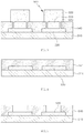
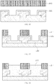
- FIG. 1 is a cross-sectional view of a semiconductor package according to an embodiment of the present invention.
- a semiconductor package according to an embodiment of the present invention may be configured in a package in a package on package (POP) type in which an upper package 400 is laminated on a lower package 300 so that the upper and lower packages can be electrically connected to each other.
- POP package on package
- the semiconductor package includes the lower package 300, the upper package 400 and a metal post 500.
- At least one lower element 370 is mounted to a lower package substrate 310
- at least one upper element 430 is mounted to an upper package substrate 410.
- the element 430 may be composed of a semiconductor.
- At this time, at least any one of the lower package substrate 310 and the upper package substrate 410 may be composed of a printed circuit board (PCB).
- PCB printed circuit board
- the lower package 300 may include the lower package substrate 310 and the lower element 370 mounted to the lower package substrate.
- the plurality of lower elements 370 may be laminated by interposing an insulating material layer therebetween.
- External terminals 350 in a solder ball form which electrically connect the semiconductor package to an external device, may be provided on a lower surface of the lower package substrate 310.
- the upper package 400 may include the upper package substrate 410 and the upper element 430 mounted to an upper surface of the upper package substrate 410.
- the upper elements 430 may be laminated by interposing an insulating material layer therebetween.
- the upper element 430 and the upper package substrate 410 may be electrically connected to each other via a plurality of bonding wires 442.
- the metal post 500 is connected to the lower package 300 which is configured as above.
- a first seed pattern portion 530 is formed on the substrate of the lower package 300, and the metal post 500 is formed on the first seed pattern portion 530.
- the metal post 500 includes at least one metal material portion 520, and at this time, the metal post is composed of a solder portion 510 of a first metal material and a metal material portion of a second metal material 520.
- the solder portion 510 is made of Sn so as to be made of a high melting point-solder material having a melting point of 230 °C to 250 °C, and the metal material portion 520 is made of a copper material.
- the general solder material When a general solder material is used, the general solder material has a melting point of 210 °C to 220 °C.
- the solder portion 510 when the solder portion 510 is made of a high melting point-solder material having a melting point of 230 °C to 250 °C, excellent bonding reliability can be obtained, and thus upon laminating the upper package 400, a stable yield rate of the process can be secured.
- the solder portion 510 is configured such that an upper surface protrudes upwardly higher than a solder resist 540 of the lower package 300.
- the metal post 500 which is configured as above is connected to the upper package 400 via a solder ball 501.
- the metal post 500 including the solder portion 510 of the high melting point-solder material is configured, a stable yield rate of the process upon limiting the upper package 400 can be ensured, and by increasing a distance between the upper package 400 and the lower package 300, high density-based lamination of the semiconductor chips may be performed, and the semiconductor package having improve reliability and stability may be formed.
- the metal post 500 is configured such that a width of an end of the metal post connected to a side of the lower package 300 is formed larger than that of an end of the metal post connected to a side of the upper package 400.
- the metal post 500 is configured such that a width of one end of the metal post connected to the solder ball 501 is formed smaller than a width of another end opposed to the one end, and at this time, the width of the metal post 500 is configured to reduce gradually from the other end to the one end.
- the metal post 500 is configured such that a width of an upper part reduces gradually from a width of the side connected to the lower package substrate 310.
- the width of the one end of the metal post 500 is formed in a size of 50% or less of that of the other end of the metal post 500, or the metal post 500 is configured to be inclined at an angle of 45° or less from the surface of the lower package substrate 310, with regard to bonding reliability with the solder ball 501, a problem is generated.
- the metal post 500 is configured such that the width of the one end is 50 to 90% of the width of the other end, or a surface in a longitudinal direction is inclined at an angle of 5° to 45° in a vertical direction in a surface of a substrate of the lower package, so that bonding reliability of the metal post 500 and the solder ball 50 can be secured.
- the metal post 500 which is formed as above, is connected to the upper package 400 via the solder ball 501 in such a manner that at least a part of an upper end of the metal post 500 is inserted into the solder ball 501.
- the metal post 500 is formed on a surface corresponding to the vertical direction in the surface of the lower package substrate 310 so as not to have a stepped cone, it is advantageous in that an electrical property can be uniformly maintained, and bonding strength with the upper package 400 can be improved with only the solder ball 501 which is smaller in the amount.
- the metal post is configured such that the width (a) of the one end of the metal post is 50% to 90% of the width (b) of the other end, the surface in a longitudinal direction is inclined at an angle of 5° to 45° in the vertical direction in the surface of a substrate of the lower package, an amount of the solder ball 501 formed on the substrate 410 of the upper package 400 can be reduced, and as bonding in a form in which the metal post 500 is surrounded by the solder ball 501 is performed, bonding reliability can be further improved.
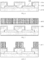
- FIG. 2 is a simplified cross-sectional view of the metal post of the semiconductor package according to the embodiment of the present invention, and the embodiment of FIG. 2 shows a structure in which the solder portion 510 of the metal post 500 protrudes upwardly higher than a solder resist pattern 540.
- FIG 2 should be understood as comprising the limitations of claim 1.
- the first seed pattern portion 530 is formed on the substrate 310, and the solder resist pattern 540 is formed on a peripheral part of the first seed pattern portion 530.
- a second seed pattern portion 535 connected to the first seed pattern portion 530 is formed on the solder resist pattern 540.
- the metal post 500 is formed on the second seed pattern portion 535.
- the metal post 500 includes the solder portion 510 and the metal material portion 520 is formed at the upper end of the metal post 510.
- the metal post 500 protrudes upwardly higher than the solder resist pattern 540.
- FIG. 3 is a simplified cross-sectional view of a metal post of a semiconductor package according to another embodiment of the present invention, and the embodiment of FIG. 3 shows a structure in which the solder portion 510 of the metal post is configured in the same plane height as the solder resist pattern 540.
- FIG 3 should be understood as comprising the limitations of claim 1.
- the first seed pattern portion 530 is formed on the substrate 310, and the solder resist pattern 540 is formed at the peripheral part of the first seed pattern portion 530.
- the second seed pattern portion 535 connected to the first seed pattern portion 530 is formed on the solder resist pattern 540, and at this time, the second seed pattern portion 535 is formed at a side except for an upper surface of the solder resist pattern 540.
- the metal post 500 is formed on the second seed pattern portion 535, and at this time, the metal post 500 includes the solder portion 510 and the metal material portion, and the solder portion 510 is configured in the same plane height as the solder resist pattern 540.
- the solder portion 510 may be made of a high welting point solder material having a melting point of 230 °C to 250 °C, such as an alloy material of Sn and Cu or an alloy material of Sn and Ag, and the metal material portion 520 is made of a copper material.
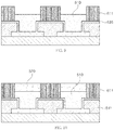
- FIGS. 4 to 12 are simplified views for explaining a method of manufacturing the metal post of the semiconductor package according to the embodiment of the present invention, namely, views for explaining the method of manufacturing the metal post of the semiconductor package according to the embodiment of FIG. 2 . These views should be understood as comprising the limitations of claim 1.
- the first seed pattern portion 530 is formed on the substrate 310, and the solder resist layer 541 is formed on the first seed pattern portion 530 which is formed as above.
- the solder resist pattern 540 is formed by patterning the solder resist layer formed on the first seed pattern portion 530.
- the second seed pattern portion 535 is formed on the solder resist pattern 540 which is formed as above.
- a photo resist layer 610 is formed on the second seed pattern portion 535, and as illustrated in FIG. 8 , a photo resist pattern 611 is formed by laminating, exposing and developing the photo resist layer 610.
- the photo resist layer 610 and the photo resist patterns 611 may be made of a dry film photo resist (DFR).
- DFR dry film photo resist
- solder portion 510 may be formed on the second seed pattern portion 535 between the photo resist pattern 611
- the adjacent photo resist pattern using a high melting point-solder material or the metal material portion 510 may be formed.
- the solder portion 510 is made of a high melting point-solder material having a melting point of 230 °C to 250 °C, such as Sn.
- the metal material portion 520 is formed by performing plating on the solder portion 510 using a metal material. At this time, the metal material portion 520 is made of a copper material.
- the metal post 500 is completed.
- a distance between the upper package and the lower package is increased by the metal post which is configured as above so that high density-based lamination of the semiconductor chips can be performed and the semiconductor package having improved reliability and stability can be provided.
- FIGS. 13 to 21 are simplified views for explaining a method of manufacturing the metal post of the semiconductor package according to another embodiment of the present invention, namely, views for explaining the metal post of the semiconductor package according to the embodiment of FIG. 3 . These views should be understood as comprising the limitations of claim 1.
- the first seed pattern portion 530 is formed on the substrate 310
- the solder resist layer 541 is formed on the first seed pattern portion 530
- the solder resist pattern 540 is formed by patterning the solder resist layer 541 formed on the first seed pattern portion 530.
- the second seed pattern portion 535 is formed on the solder resist pattern 540 which is formed as above, and as illustrated in FIG. 16 , the photo resist layer 610 is formed on the second seed pattern portion 535, and as illustrated in FIG. 17 , the photo resist patterns 611 are formed by laminating, exposing and developing the photo resist layer 610.
- the photo resist layer 610 and the photo resist pattern 611 may be formed of DFR (Dry Film PhotoResist).
- the metal post 510 is formed by filling the first pattern portion 530 and the second seed pattern portion 535 between the photo resist pattern 611 and the adjacent resist pattern with a metal material, and Cu may be used as a metal material for forming the metal post 510.
- the second seed pattern portion 535 is exposed by removing the photo resist patterns 611, and as illustrated in FIG. 20 , the metal post is formed by removing the exposed second seed pattern portion 535.
- the surface treatment layer 520 may be formed on the upper surface and the side of the metal post 510.
- the number of mounted chips is increased so that high density can be realized, and the semiconductor package having bonding reliability between the upper package and the lower package can be provided.
Landscapes
- Wire Bonding (AREA)
Applications Claiming Priority (3)
| Application Number | Priority Date | Filing Date | Title |
|---|---|---|---|
| KR1020130110974A KR102109042B1 (ko) | 2013-09-16 | 2013-09-16 | 반도체 패키지 |
| KR1020130115332A KR102093927B1 (ko) | 2013-09-27 | 2013-09-27 | 반도체 패키지 |
| KR1020130115333A KR102091619B1 (ko) | 2013-09-27 | 2013-09-27 | 반도체 패키지 |
Publications (3)
| Publication Number | Publication Date |
|---|---|
| EP2849226A2 EP2849226A2 (en) | 2015-03-18 |
| EP2849226A3 EP2849226A3 (en) | 2015-04-29 |
| EP2849226B1 true EP2849226B1 (en) | 2018-08-22 |
Family
ID=51518709
Family Applications (1)
| Application Number | Title | Priority Date | Filing Date |
|---|---|---|---|
| EP14184685.7A Active EP2849226B1 (en) | 2013-09-16 | 2014-09-12 | Semiconductor package |
Country Status (5)
| Country | Link |
|---|---|
| US (1) | US9252112B2 (https=) |
| EP (1) | EP2849226B1 (https=) |
| JP (1) | JP6419500B2 (https=) |
| CN (1) | CN104465580B (https=) |
| TW (1) | TWI646639B (https=) |
Families Citing this family (4)
| Publication number | Priority date | Publication date | Assignee | Title |
|---|---|---|---|---|
| TWI517269B (zh) * | 2013-09-27 | 2016-01-11 | 矽品精密工業股份有限公司 | 層疊式封裝結構及其製法 |
| KR102152865B1 (ko) * | 2014-02-06 | 2020-09-07 | 엘지이노텍 주식회사 | 인쇄회로기판, 이를 포함하는 패키지 기판 및 이의 제조 방법 |
| JP2016171190A (ja) * | 2015-03-12 | 2016-09-23 | イビデン株式会社 | パッケージ−オン−パッケージ用プリント配線板 |
| KR102446861B1 (ko) | 2017-09-21 | 2022-09-23 | 삼성전자주식회사 | 적층 패키지 및 그의 제조 방법 |
Family Cites Families (17)
| Publication number | Priority date | Publication date | Assignee | Title |
|---|---|---|---|---|
| JPH11145327A (ja) * | 1997-11-07 | 1999-05-28 | Shinko Electric Ind Co Ltd | 半導体装置および該半導体装置の実装構造 |
| US6818545B2 (en) * | 2001-03-05 | 2004-11-16 | Megic Corporation | Low fabrication cost, fine pitch and high reliability solder bump |
| JP2007194436A (ja) * | 2006-01-19 | 2007-08-02 | Elpida Memory Inc | 半導体パッケージ、導電性ポスト付き基板、積層型半導体装置、半導体パッケージの製造方法及び積層型半導体装置の製造方法 |
| JP4917874B2 (ja) * | 2006-12-13 | 2012-04-18 | 新光電気工業株式会社 | 積層型パッケージ及びその製造方法 |
| JP5003260B2 (ja) * | 2007-04-13 | 2012-08-15 | 日本電気株式会社 | 半導体装置およびその製造方法 |
| JP5217043B2 (ja) * | 2007-07-11 | 2013-06-19 | ルネサスエレクトロニクス株式会社 | 半導体装置の製造方法 |
| JP5056718B2 (ja) * | 2008-10-16 | 2012-10-24 | 株式会社デンソー | 電子装置の製造方法 |
| JP5193898B2 (ja) * | 2009-02-12 | 2013-05-08 | 新光電気工業株式会社 | 半導体装置及び電子装置 |
| KR20100121231A (ko) * | 2009-05-08 | 2010-11-17 | 삼성전자주식회사 | 회로패턴 들뜸 현상을 억제하는 패키지 온 패키지 및 그 제조방법 |
| US20110024899A1 (en) * | 2009-07-28 | 2011-02-03 | Kenji Masumoto | Substrate structure for cavity package |
| US8482111B2 (en) * | 2010-07-19 | 2013-07-09 | Tessera, Inc. | Stackable molded microelectronic packages |
| JP5599276B2 (ja) * | 2010-09-24 | 2014-10-01 | 新光電気工業株式会社 | 半導体素子、半導体素子実装体及び半導体素子の製造方法 |
| JP5462777B2 (ja) * | 2010-12-09 | 2014-04-02 | 日本特殊陶業株式会社 | 多層配線基板の製造方法 |
| US8531021B2 (en) * | 2011-01-27 | 2013-09-10 | Unimicron Technology Corporation | Package stack device and fabrication method thereof |
| KR101167805B1 (ko) * | 2011-04-25 | 2012-07-25 | 삼성전기주식회사 | 패키지 기판 및 이의 제조방법 |
| JP5906812B2 (ja) * | 2012-02-29 | 2016-04-20 | 富士通株式会社 | 配線構造、半導体装置及び配線構造の製造方法 |
| US9368438B2 (en) * | 2012-12-28 | 2016-06-14 | Taiwan Semiconductor Manufacturing Company, Ltd. | Package on package (PoP) bonding structures |
-
2014
- 2014-09-12 TW TW103131554A patent/TWI646639B/zh active
- 2014-09-12 EP EP14184685.7A patent/EP2849226B1/en active Active
- 2014-09-16 CN CN201410471924.XA patent/CN104465580B/zh active Active
- 2014-09-16 JP JP2014187826A patent/JP6419500B2/ja active Active
- 2014-09-16 US US14/487,793 patent/US9252112B2/en active Active
Non-Patent Citations (1)
| Title |
|---|
| None * |
Also Published As
| Publication number | Publication date |
|---|---|
| US20150076691A1 (en) | 2015-03-19 |
| JP6419500B2 (ja) | 2018-11-07 |
| TWI646639B (zh) | 2019-01-01 |
| TW201517222A (zh) | 2015-05-01 |
| US9252112B2 (en) | 2016-02-02 |
| CN104465580A (zh) | 2015-03-25 |
| EP2849226A3 (en) | 2015-04-29 |
| CN104465580B (zh) | 2017-08-04 |
| EP2849226A2 (en) | 2015-03-18 |
| JP2015057827A (ja) | 2015-03-26 |
Similar Documents
| Publication | Publication Date | Title |
|---|---|---|
| US20220051973A1 (en) | Semiconductor package and manufacturing method thereof | |
| US8399992B2 (en) | Package-on-package type semiconductor package | |
| EP2227076A1 (en) | Multilayer circuit board and production method thereof and communication device | |
| CN111933590B (zh) | 封装结构和封装结构制作方法 | |
| KR20140075357A (ko) | 칩 내장형 인쇄회로기판과 그를 이용한 반도체 패키지 및 칩 내장형 인쇄회로기판의 제조방법 | |
| KR20120007839A (ko) | 적층형 반도체 패키지의 제조방법 | |
| KR20150009826A (ko) | 소자 내장형 패키지 기판 및 이를 포함하는 반도체 패키지 | |
| US10483194B2 (en) | Interposer substrate and method of fabricating the same | |
| EP2849226B1 (en) | Semiconductor package | |
| CN105009279B (zh) | 半导体器件及制造半导体器件的方法 | |
| KR102093927B1 (ko) | 반도체 패키지 | |
| KR20220045128A (ko) | 반도체 패키지 | |
| KR102472045B1 (ko) | 반도체 패키지 | |
| KR20140078198A (ko) | 패키지 온 패키지형 반도체 패키지 및 그 제조 방법 | |
| KR102026227B1 (ko) | 패키지 온 패키지형 반도체 패키지 및 그 제조방법 | |
| KR102091619B1 (ko) | 반도체 패키지 | |
| KR102109042B1 (ko) | 반도체 패키지 | |
| KR101432488B1 (ko) | 적층형 반도체 패키지 및 그 제조방법 | |
| KR20140077360A (ko) | 패키지 온 패키지형 반도체 패키지 및 그 제조 방법 | |
| KR20140076089A (ko) | 반도체 기판 및 그 제조 방법, 그리고 반도체 패키지 |
Legal Events
| Date | Code | Title | Description |
|---|---|---|---|
| PUAI | Public reference made under article 153(3) epc to a published international application that has entered the european phase |
Free format text: ORIGINAL CODE: 0009012 |
|
| 17P | Request for examination filed |
Effective date: 20140912 |
|
| AK | Designated contracting states |
Kind code of ref document: A2 Designated state(s): AL AT BE BG CH CY CZ DE DK EE ES FI FR GB GR HR HU IE IS IT LI LT LU LV MC MK MT NL NO PL PT RO RS SE SI SK SM TR |
|
| AX | Request for extension of the european patent |
Extension state: BA ME |
|
| PUAL | Search report despatched |
Free format text: ORIGINAL CODE: 0009013 |
|
| AK | Designated contracting states |
Kind code of ref document: A3 Designated state(s): AL AT BE BG CH CY CZ DE DK EE ES FI FR GB GR HR HU IE IS IT LI LT LU LV MC MK MT NL NO PL PT RO RS SE SI SK SM TR |
|
| AX | Request for extension of the european patent |
Extension state: BA ME |
|
| RIC1 | Information provided on ipc code assigned before grant |
Ipc: H01L 23/498 20060101AFI20150326BHEP Ipc: H01L 25/10 20060101ALI20150326BHEP |
|
| R17P | Request for examination filed (corrected) |
Effective date: 20151028 |
|
| RBV | Designated contracting states (corrected) |
Designated state(s): AL AT BE BG CH CY CZ DE DK EE ES FI FR GB GR HR HU IE IS IT LI LT LU LV MC MK MT NL NO PL PT RO RS SE SI SK SM TR |
|
| STAA | Information on the status of an ep patent application or granted ep patent |
Free format text: STATUS: EXAMINATION IS IN PROGRESS |
|
| 17Q | First examination report despatched |
Effective date: 20170127 |
|
| RAP1 | Party data changed (applicant data changed or rights of an application transferred) |
Owner name: LG INNOTEK CO., LTD. |
|
| GRAP | Despatch of communication of intention to grant a patent |
Free format text: ORIGINAL CODE: EPIDOSNIGR1 |
|
| STAA | Information on the status of an ep patent application or granted ep patent |
Free format text: STATUS: GRANT OF PATENT IS INTENDED |
|
| INTG | Intention to grant announced |
Effective date: 20180322 |
|
| GRAS | Grant fee paid |
Free format text: ORIGINAL CODE: EPIDOSNIGR3 |
|
| GRAA | (expected) grant |
Free format text: ORIGINAL CODE: 0009210 |
|
| STAA | Information on the status of an ep patent application or granted ep patent |
Free format text: STATUS: THE PATENT HAS BEEN GRANTED |
|
| AK | Designated contracting states |
Kind code of ref document: B1 Designated state(s): AL AT BE BG CH CY CZ DE DK EE ES FI FR GB GR HR HU IE IS IT LI LT LU LV MC MK MT NL NO PL PT RO RS SE SI SK SM TR |
|
| REG | Reference to a national code |
Ref country code: GB Ref legal event code: FG4D |
|
| REG | Reference to a national code |
Ref country code: CH Ref legal event code: EP |
|
| REG | Reference to a national code |
Ref country code: AT Ref legal event code: REF Ref document number: 1033436 Country of ref document: AT Kind code of ref document: T Effective date: 20180915 |
|
| REG | Reference to a national code |
Ref country code: IE Ref legal event code: FG4D |
|
| REG | Reference to a national code |
Ref country code: DE Ref legal event code: R096 Ref document number: 602014030757 Country of ref document: DE |
|
| REG | Reference to a national code |
Ref country code: NL Ref legal event code: MP Effective date: 20180822 |
|
| REG | Reference to a national code |
Ref country code: LT Ref legal event code: MG4D |
|
| PG25 | Lapsed in a contracting state [announced via postgrant information from national office to epo] |
Ref country code: IS Free format text: LAPSE BECAUSE OF FAILURE TO SUBMIT A TRANSLATION OF THE DESCRIPTION OR TO PAY THE FEE WITHIN THE PRESCRIBED TIME-LIMIT Effective date: 20181222 Ref country code: BG Free format text: LAPSE BECAUSE OF FAILURE TO SUBMIT A TRANSLATION OF THE DESCRIPTION OR TO PAY THE FEE WITHIN THE PRESCRIBED TIME-LIMIT Effective date: 20181122 Ref country code: NL Free format text: LAPSE BECAUSE OF FAILURE TO SUBMIT A TRANSLATION OF THE DESCRIPTION OR TO PAY THE FEE WITHIN THE PRESCRIBED TIME-LIMIT Effective date: 20180822 Ref country code: LT Free format text: LAPSE BECAUSE OF FAILURE TO SUBMIT A TRANSLATION OF THE DESCRIPTION OR TO PAY THE FEE WITHIN THE PRESCRIBED TIME-LIMIT Effective date: 20180822 Ref country code: GR Free format text: LAPSE BECAUSE OF FAILURE TO SUBMIT A TRANSLATION OF THE DESCRIPTION OR TO PAY THE FEE WITHIN THE PRESCRIBED TIME-LIMIT Effective date: 20181123 Ref country code: NO Free format text: LAPSE BECAUSE OF FAILURE TO SUBMIT A TRANSLATION OF THE DESCRIPTION OR TO PAY THE FEE WITHIN THE PRESCRIBED TIME-LIMIT Effective date: 20181122 Ref country code: SE Free format text: LAPSE BECAUSE OF FAILURE TO SUBMIT A TRANSLATION OF THE DESCRIPTION OR TO PAY THE FEE WITHIN THE PRESCRIBED TIME-LIMIT Effective date: 20180822 Ref country code: RS Free format text: LAPSE BECAUSE OF FAILURE TO SUBMIT A TRANSLATION OF THE DESCRIPTION OR TO PAY THE FEE WITHIN THE PRESCRIBED TIME-LIMIT Effective date: 20180822 Ref country code: FI Free format text: LAPSE BECAUSE OF FAILURE TO SUBMIT A TRANSLATION OF THE DESCRIPTION OR TO PAY THE FEE WITHIN THE PRESCRIBED TIME-LIMIT Effective date: 20180822 |
|
| REG | Reference to a national code |
Ref country code: AT Ref legal event code: MK05 Ref document number: 1033436 Country of ref document: AT Kind code of ref document: T Effective date: 20180822 |
|
| PG25 | Lapsed in a contracting state [announced via postgrant information from national office to epo] |
Ref country code: HR Free format text: LAPSE BECAUSE OF FAILURE TO SUBMIT A TRANSLATION OF THE DESCRIPTION OR TO PAY THE FEE WITHIN THE PRESCRIBED TIME-LIMIT Effective date: 20180822 Ref country code: AL Free format text: LAPSE BECAUSE OF FAILURE TO SUBMIT A TRANSLATION OF THE DESCRIPTION OR TO PAY THE FEE WITHIN THE PRESCRIBED TIME-LIMIT Effective date: 20180822 Ref country code: LV Free format text: LAPSE BECAUSE OF FAILURE TO SUBMIT A TRANSLATION OF THE DESCRIPTION OR TO PAY THE FEE WITHIN THE PRESCRIBED TIME-LIMIT Effective date: 20180822 |
|
| PG25 | Lapsed in a contracting state [announced via postgrant information from national office to epo] |
Ref country code: CZ Free format text: LAPSE BECAUSE OF FAILURE TO SUBMIT A TRANSLATION OF THE DESCRIPTION OR TO PAY THE FEE WITHIN THE PRESCRIBED TIME-LIMIT Effective date: 20180822 Ref country code: IT Free format text: LAPSE BECAUSE OF FAILURE TO SUBMIT A TRANSLATION OF THE DESCRIPTION OR TO PAY THE FEE WITHIN THE PRESCRIBED TIME-LIMIT Effective date: 20180822 Ref country code: RO Free format text: LAPSE BECAUSE OF FAILURE TO SUBMIT A TRANSLATION OF THE DESCRIPTION OR TO PAY THE FEE WITHIN THE PRESCRIBED TIME-LIMIT Effective date: 20180822 Ref country code: PL Free format text: LAPSE BECAUSE OF FAILURE TO SUBMIT A TRANSLATION OF THE DESCRIPTION OR TO PAY THE FEE WITHIN THE PRESCRIBED TIME-LIMIT Effective date: 20180822 Ref country code: AT Free format text: LAPSE BECAUSE OF FAILURE TO SUBMIT A TRANSLATION OF THE DESCRIPTION OR TO PAY THE FEE WITHIN THE PRESCRIBED TIME-LIMIT Effective date: 20180822 Ref country code: EE Free format text: LAPSE BECAUSE OF FAILURE TO SUBMIT A TRANSLATION OF THE DESCRIPTION OR TO PAY THE FEE WITHIN THE PRESCRIBED TIME-LIMIT Effective date: 20180822 Ref country code: ES Free format text: LAPSE BECAUSE OF FAILURE TO SUBMIT A TRANSLATION OF THE DESCRIPTION OR TO PAY THE FEE WITHIN THE PRESCRIBED TIME-LIMIT Effective date: 20180822 |
|
| REG | Reference to a national code |
Ref country code: CH Ref legal event code: PL |
|
| REG | Reference to a national code |
Ref country code: DE Ref legal event code: R097 Ref document number: 602014030757 Country of ref document: DE |
|
| PG25 | Lapsed in a contracting state [announced via postgrant information from national office to epo] |
Ref country code: SM Free format text: LAPSE BECAUSE OF FAILURE TO SUBMIT A TRANSLATION OF THE DESCRIPTION OR TO PAY THE FEE WITHIN THE PRESCRIBED TIME-LIMIT Effective date: 20180822 Ref country code: SK Free format text: LAPSE BECAUSE OF FAILURE TO SUBMIT A TRANSLATION OF THE DESCRIPTION OR TO PAY THE FEE WITHIN THE PRESCRIBED TIME-LIMIT Effective date: 20180822 Ref country code: DK Free format text: LAPSE BECAUSE OF FAILURE TO SUBMIT A TRANSLATION OF THE DESCRIPTION OR TO PAY THE FEE WITHIN THE PRESCRIBED TIME-LIMIT Effective date: 20180822 |
|
| REG | Reference to a national code |
Ref country code: BE Ref legal event code: MM Effective date: 20180930 |
|
| REG | Reference to a national code |
Ref country code: IE Ref legal event code: MM4A |
|
| PG25 | Lapsed in a contracting state [announced via postgrant information from national office to epo] |
Ref country code: LU Free format text: LAPSE BECAUSE OF NON-PAYMENT OF DUE FEES Effective date: 20180912 Ref country code: MC Free format text: LAPSE BECAUSE OF FAILURE TO SUBMIT A TRANSLATION OF THE DESCRIPTION OR TO PAY THE FEE WITHIN THE PRESCRIBED TIME-LIMIT Effective date: 20180822 |
|
| PLBE | No opposition filed within time limit |
Free format text: ORIGINAL CODE: 0009261 |
|
| STAA | Information on the status of an ep patent application or granted ep patent |
Free format text: STATUS: NO OPPOSITION FILED WITHIN TIME LIMIT |
|
| GBPC | Gb: european patent ceased through non-payment of renewal fee |
Effective date: 20181122 |
|
| 26N | No opposition filed |
Effective date: 20190523 |
|
| PG25 | Lapsed in a contracting state [announced via postgrant information from national office to epo] |
Ref country code: IE Free format text: LAPSE BECAUSE OF NON-PAYMENT OF DUE FEES Effective date: 20180912 |
|
| PG25 | Lapsed in a contracting state [announced via postgrant information from national office to epo] |
Ref country code: BE Free format text: LAPSE BECAUSE OF NON-PAYMENT OF DUE FEES Effective date: 20180930 Ref country code: SI Free format text: LAPSE BECAUSE OF FAILURE TO SUBMIT A TRANSLATION OF THE DESCRIPTION OR TO PAY THE FEE WITHIN THE PRESCRIBED TIME-LIMIT Effective date: 20180822 Ref country code: LI Free format text: LAPSE BECAUSE OF NON-PAYMENT OF DUE FEES Effective date: 20180930 Ref country code: FR Free format text: LAPSE BECAUSE OF NON-PAYMENT OF DUE FEES Effective date: 20181022 Ref country code: CH Free format text: LAPSE BECAUSE OF NON-PAYMENT OF DUE FEES Effective date: 20180930 |
|
| PG25 | Lapsed in a contracting state [announced via postgrant information from national office to epo] |
Ref country code: GB Free format text: LAPSE BECAUSE OF NON-PAYMENT OF DUE FEES Effective date: 20181122 |
|
| PG25 | Lapsed in a contracting state [announced via postgrant information from national office to epo] |
Ref country code: MT Free format text: LAPSE BECAUSE OF NON-PAYMENT OF DUE FEES Effective date: 20180912 |
|
| PG25 | Lapsed in a contracting state [announced via postgrant information from national office to epo] |
Ref country code: TR Free format text: LAPSE BECAUSE OF FAILURE TO SUBMIT A TRANSLATION OF THE DESCRIPTION OR TO PAY THE FEE WITHIN THE PRESCRIBED TIME-LIMIT Effective date: 20180822 |
|
| PG25 | Lapsed in a contracting state [announced via postgrant information from national office to epo] |
Ref country code: PT Free format text: LAPSE BECAUSE OF FAILURE TO SUBMIT A TRANSLATION OF THE DESCRIPTION OR TO PAY THE FEE WITHIN THE PRESCRIBED TIME-LIMIT Effective date: 20180822 Ref country code: HU Free format text: LAPSE BECAUSE OF FAILURE TO SUBMIT A TRANSLATION OF THE DESCRIPTION OR TO PAY THE FEE WITHIN THE PRESCRIBED TIME-LIMIT; INVALID AB INITIO Effective date: 20140912 |
|
| PG25 | Lapsed in a contracting state [announced via postgrant information from national office to epo] |
Ref country code: MK Free format text: LAPSE BECAUSE OF NON-PAYMENT OF DUE FEES Effective date: 20180822 Ref country code: CY Free format text: LAPSE BECAUSE OF FAILURE TO SUBMIT A TRANSLATION OF THE DESCRIPTION OR TO PAY THE FEE WITHIN THE PRESCRIBED TIME-LIMIT Effective date: 20180822 |
|
| PGFP | Annual fee paid to national office [announced via postgrant information from national office to epo] |
Ref country code: DE Payment date: 20250820 Year of fee payment: 12 |
|
| REG | Reference to a national code |
Ref country code: DE Ref legal event code: R079 Ref document number: 602014030757 Country of ref document: DE Free format text: PREVIOUS MAIN CLASS: H01L0023498000 Ipc: H10W0070620000 |