EP2831694B1 - A pulse clock generation logic with built-in level shifter and programmable rising edge and pulse width - Google Patents
A pulse clock generation logic with built-in level shifter and programmable rising edge and pulse width Download PDFInfo
- Publication number
- EP2831694B1 EP2831694B1 EP13715579.2A EP13715579A EP2831694B1 EP 2831694 B1 EP2831694 B1 EP 2831694B1 EP 13715579 A EP13715579 A EP 13715579A EP 2831694 B1 EP2831694 B1 EP 2831694B1
- Authority
- EP
- European Patent Office
- Prior art keywords
- pulse clock
- pulse
- delay
- logic
- clock generation
- Prior art date
- Legal status (The legal status is an assumption and is not a legal conclusion. Google has not performed a legal analysis and makes no representation as to the accuracy of the status listed.)
- Not-in-force
Links
Images

Classifications
-
- G—PHYSICS
- G06—COMPUTING OR CALCULATING; COUNTING
- G06F—ELECTRIC DIGITAL DATA PROCESSING
- G06F1/00—Details not covered by groups G06F3/00 - G06F13/00 and G06F21/00
- G06F1/04—Generating or distributing clock signals or signals derived directly therefrom
-
- G—PHYSICS
- G11—INFORMATION STORAGE
- G11C—STATIC STORES
- G11C11/00—Digital stores characterised by the use of particular electric or magnetic storage elements; Storage elements therefor
- G11C11/21—Digital stores characterised by the use of particular electric or magnetic storage elements; Storage elements therefor using electric elements
- G11C11/34—Digital stores characterised by the use of particular electric or magnetic storage elements; Storage elements therefor using electric elements using semiconductor devices
- G11C11/40—Digital stores characterised by the use of particular electric or magnetic storage elements; Storage elements therefor using electric elements using semiconductor devices using transistors
- G11C11/41—Digital stores characterised by the use of particular electric or magnetic storage elements; Storage elements therefor using electric elements using semiconductor devices using transistors forming static cells with positive feedback, i.e. cells not needing refreshing or charge regeneration, e.g. bistable multivibrator or Schmitt trigger
- G11C11/413—Auxiliary circuits, e.g. for addressing, decoding, driving, writing, sensing, timing or power reduction
- G11C11/417—Auxiliary circuits, e.g. for addressing, decoding, driving, writing, sensing, timing or power reduction for memory cells of the field-effect type
- G11C11/418—Address circuits
-
- G—PHYSICS
- G11—INFORMATION STORAGE
- G11C—STATIC STORES
- G11C11/00—Digital stores characterised by the use of particular electric or magnetic storage elements; Storage elements therefor
- G11C11/21—Digital stores characterised by the use of particular electric or magnetic storage elements; Storage elements therefor using electric elements
- G11C11/34—Digital stores characterised by the use of particular electric or magnetic storage elements; Storage elements therefor using electric elements using semiconductor devices
- G11C11/40—Digital stores characterised by the use of particular electric or magnetic storage elements; Storage elements therefor using electric elements using semiconductor devices using transistors
- G11C11/41—Digital stores characterised by the use of particular electric or magnetic storage elements; Storage elements therefor using electric elements using semiconductor devices using transistors forming static cells with positive feedback, i.e. cells not needing refreshing or charge regeneration, e.g. bistable multivibrator or Schmitt trigger
- G11C11/413—Auxiliary circuits, e.g. for addressing, decoding, driving, writing, sensing, timing or power reduction
- G11C11/417—Auxiliary circuits, e.g. for addressing, decoding, driving, writing, sensing, timing or power reduction for memory cells of the field-effect type
- G11C11/419—Read-write [R-W] circuits
-
- G—PHYSICS
- G11—INFORMATION STORAGE
- G11C—STATIC STORES
- G11C7/00—Arrangements for writing information into, or reading information out from, a digital store
- G11C7/22—Read-write [R-W] timing or clocking circuits; Read-write [R-W] control signal generators or management
- G11C7/222—Clock generating, synchronizing or distributing circuits within memory device
Definitions
- Disclosed embodiments generally relate to pulse clock generation. More particularly, exemplary embodiments are directed to generating pulse clocks with programmable edges and pulse widths configured for varying requirements of different memory access operations.
- T-SRAM 6 Transistor Static Random Access Memory
- 6T-SRAM 6 Transistor Static Random Access Memory
- a common solution involves the use of multiple voltage domains, such that memory cells may be operated at a relatively high voltage level while other on-chip logic may be operated at lower voltages.
- level shifters are commonly used to convert low voltage to high voltage and vice versa as needed.
- level shifters introduce latency, which may be undesirable in timing critical paths.
- Document US6850460 discloses a SRAM array local clock generator having variable delay settings that are programmable via level scan bits. Program bits from the level scan operation are decoded and used to adjust the number of delay elements in the local clock generator path.
- pulse clocks are often utilized to overcome the effects of device variations (e.g. due to process variations). These pulse clocks may be subjected to conflicting needs for different memory access operations. For example, during a memory read operation it may be desirable for the rising edge of the pulse clock to arrive as fast as possible at memory cells of the memory array being accessed, in order to enable quick read access. Moreover, during the memory read operation it may be desirable for the pulse width of the pulse clock to be narrow, in order to reduce power consumption by disallowing full voltage swings on bit lines.
- memory write operations are usually not timing critical, and thus can tolerate higher arrival delays in the rising edge of the pulse clock.
- memory write operations may benefit from delays in the pulse clock so as to allow sufficient set-up time for the data written.
- the pulse width of the pulse clock may be wider to allow for sufficient write time in order to guarantee successful completion of the write operations, especially at lower supply voltage levels.
- Conventional pulse clock implementations are not well suited to meet these conflicting needs for read and write operations on memory cells.
- Exemplary embodiments of the invention are directed to circuits and methods for generating pulse clocks with programmable edges and pulse widths configured for varying requirements of different memory access operations.
- an exemplary embodiment is directed to a method for generating a pulse clock comprising: configuring a programmable rising edge delay of the pulse clock; configuring a programmable pulse width of the pulse clock; configuring a level shifter for shifting a voltage level of the pulse clock; and generating the pulse clock in accordance with the programmed rising edge delay, programmed pulse width, and shifted voltage level.
- Another exemplary embodiment is directed to a pulse clock generation circuit comprising: a selective delay logic to provide a programmable rising edge delay of the pulse clock; a selective pulse width widening logic to provide a programmable pulse width of the pulse clock; a built-in level shifter configured to shift a voltage level of the pulse clock; and logic configured to generate the pulse clock in accordance with the programmed rising edge delay, programmed pulse width, and shifted voltage level.
- Yet another exemplary embodiment is directed to non-transitory computer-readable storage medium comprising code, which, when executed by a processor, causes the processor to perform operations for programming a pulse clock generator, the non-transitory computer-readable storage medium comprising: code for configuring a programmable rising edge delay of the pulse clock; code for configuring a programmable pulse width of the pulse clock; code for configuring a level shifter for shifting a voltage level of the pulse clock; and code for generating the pulse clock in accordance with the programmed rising edge delay, programmed pulse width, and shifted voltage level.
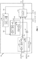
- Exemplary embodiments are directed to self-timed pulse clock generation circuits configured for programmable pulse width and rising edge delays in order to meet conflicting requirements of read and write operations. Further, exemplary embodiments may include a built-in level shifter configured to convert a raw clock in a low voltage domain to pulse clocks for read and write operations in high voltage domain without introducing additional delays from a separate voltage level shifter, while also preventing glitches and charge sharing problems which may occur in conventional implementations.
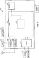
- Raw clock 122 may be input to self-timed pulse clock generation circuit 100, and may serve as a base clock for generating customized clock pulses for read and write operations.
- Raw clock 122 may be generated by known techniques such as by the use of piezoelectric crystals, etc.
- Raw clock 122 may be made available at a low voltage level or may be derived from a low voltage domain.
- Raw clock 122 may first enter selective delay logic 102, wherein raw clock 122 may be delayed selectively for write operations.
- Programmable delay logic 104, read/write control 126 and selector 106 may be configured as shown for selectively delaying raw clock 122. In one example, if a read operation is indicated by read/write control 126, then raw clock 122 may be selected by selector 106 to form the selectively delayed output clock clk_d1 116. On the other hand, if read/write control 126 indicates a write operation, then programmable delay logic 104 may delay raw clock 122 by a desired amount and generate a delayed clock 124, which may then be selected by selector 106 to form the selectively delayed output clock clk_d1 116.
- Programmable delay logic 104 may be implemented by known techniques, such as, by controlling a number of inverters or buffer elements to be coupled in series. Effective sizes of these inverters or buffer elements may also be controlled to adjust the delay amount. Skilled persons will recognize suitable implementations for programmable delay logic 104.
- Pulse clock generation logic 112 may ultimately output pulse clock 114 which meets above-noted requirements for read and write operations in exemplary embodiments.
- Pulse clock generation logic 112 may include logic for voltage level shifting, such that output pulse clock 114 is made available at a high voltage level without introducing unwanted latency from a separate voltage level shifter. Further, pulse clock generation logic 112 may be configured to eliminate glitches in output pulse clock 114.
- Feedback path 118 from output pulse clock 114 back to pulse clock generation logic 112 through reset 121 may include read delay mimic logic 108 and selective pulse width widening logic 110 as shown. Feedback path 118 may provide a self-resetting and thus self-timing functionality to pulse clock generation logic 112. Pulse clock generation logic 112, read delay mimic logic 108, and selective pulse width widening logic 110 will now be described in further detail.
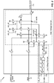
- pulse clock generation logic 112 includes a transistor-level schematic.
- Enable 130 and power-up reset 128 are input to clock generation logic 112 from an external source (not shown) to enable or reset the output pulse clock 114.
- An exemplary operation of pulse clock generation logic 112 will now be described. Initially, power-up reset 128 is driven high, thus causing the output of inverter i6 to be driven low and triggering pull-up transistor p3 to pull up lat_node 142 and thereby driving output pulse clock 114 low via inverter i5. It will be observed that pull-up transistor p3 is in the high voltage domain, as indicated in FIG. 2 . Thus, output pulse clock 114 is derived in the high voltage domain.
- a first instance of a rising edge of raw clock 122 will now be considered. It will be recalled that the selectively delayed output clock clk_d1 116 is a selectively delayed version of raw clock 122. Both raw clock 122 and selectively delayed output clock clk_d1 116 may be in the low voltage domain. Thus, a rising edge of raw clock 122 may cause a rising edge of selectively delayed output clock clk_d1 116 after a delay, and then turn on pull-down transistor n1. At this instance in time pull-down transistor n3 will remain turned off. It will be noticed from FIG.
- pull-up transistors p5 and p6 will be partially turned off, because the source voltages of pull-up transistors p5 and p6 are in the high voltage domain and their gate voltages are in the low voltage domain; and all four pull-down transistors n0, n1, n2, and n4 will be turned on at this instance. Therefore, both nodes int_node 144 and lat_node 142 will be pulled down and inverter i5 will drive output pulse clock 114 high.
- pull-down transistor n3 will be turned on, which will provide additional current source to speed up the pull down process of lat_node 142 and int_node 144 .
- output pulse clock 114 is already in the high voltage domain. Accordingly, the rising edge of raw clock 122 in the low voltage domain creates a rising edge of output pulse clock 114 in the high voltage domain without requiring additional voltage level shifting logic. While pull-up transistors p5 and p6 being turned off halfway may incur minor delay and power consumption costs, these costs may be offset by the additional pull-down path provided by pull-down transistors n3 and n4.
- lat_node 142 will remain in the low state and pulse clock 114 will remain in the high state due to the latch created by inverter i4 and the combination of pull-up transistors p4, p6 and pull-down transistors n3, n4, until a reset mechanism returns lat_node 142 to high state, thus driving output pulse clock 114 low.
- Reset 121 which will be described in further detail below, can control the falling edge of output pulse clock 114. It will be recognized that controlling the time period between the rising edge of output pulse clock 114 and the falling edge of output pulse clock 114 will determine the width of the clock pulse derived at output pulse clock 114.
- selective pulse width widening logic 110 may be employed to selectively expand the pulse width between rising and falling edges of output pulse clock 114. Similar to selective delay logic 102, selective pulse width widening logic 110 may employ multiplexor 107 to choose between the input signal without added delays and a delayed version of the input signal, based on read/write control 126. The timing of read/write control 126 may be appropriately adjusted by buffer 127 to account for delays in reaching selective pulse width widening block 110 after passing through selective delay block 102 which was previously discussed. Accordingly, depending on whether the operation is a read or a write, the delay path through selective pulse width widening logic may be controlled, such that the pulse width for write operations is made wider.
- output 120 of read delay mimic logic 108 may be selectively delayed to cause the width of the output of selective pulse width widening logic 110, reset 121 to change. This will control the time it takes for reset 121 to rise from a low to high level and then fall back to the low level.
- a next rising edge of output pulse clock 114 may be generated by repeating the above process.
- the next falling edge may be suitably delayed for read operations by read delay mimic logic 108.
- read delay mimic logic 108 is configured to ultimately delay the falling edge of output pulse clock 114, thus controlling the pulse width.
- the rising edge of output pulse clock 114 is controlled by selective delay logic 102.
- feedback path 118 from output pulse clock 114 to reset 121 will now be described. As shown in FIG. 1 , this path comprises read delay mimic logic 108 and selective pulse width widening logic 110.
- Read delay mimic logic 108 may be included to control the delay in the falling edge of output pulse clock 114 from the rising edge of output pulse clock 114 in order to account for memory array access delays encountered during a read operation.
- read delay mimic logic 108 may be configured to provide a delay corresponding to the delay which may be incurred in accessing a memory cell in the memory array.
- Read delay mimic logic may comprise a programmable delay element to match an expected read access delay. Thus, the rising edge of output pulse clock 114 will be delayed by read delay mimic logic 108 to form the rising edge of output 120.
- selective pulse width widening logic 110 will select the input without any delay added and the rising edge of output 120 will essentially appear as the rising edge of reset 121, which is inverted by inverter i7 in pulse clock generation logic 112.
- the inverter formed by pull-up transistor p0 and pull-down transistor n0 will reset lat_node 142 to a high state.
- the feedback loop including read mimic delay logic 108 of FIG. 1 will essentially ensure that the falling edge of output pulse clock 114 is made available at a delayed time in the high voltage domain in the case of read operations.
- node clk_d2 140 will fall after the rising edge of selectively delayed output clock clk_d1 116 traverses inverters i1, i2, i3, and nand1 and nor1. This will cause pull-down transistor n2 to be turned off, and also pull-up transistor p6 to be turned on. This will cause lat_node 142 to rise, thus creating the falling edge of output pulse clock 114. At this point in time, pull-down transistor n1 may either be turned on or off, without affecting the latching function of lat_node 142.
- selective pulse width widening logic 110 will selectively introduce an additional delay in the feedback path before reset 121 may be asserted and thus allowing lat_node 142 to rise and create the falling edge of output pulse clock 114. In this manner, write operations will have a wider pulse width. As previously described, a wider pulse width may facilitate write operations by providing additional time for completion of write operations (which as will be recalled, are usually not timing critical).
- pull-down transistors n1 and n2 are a self-timed process.
- the time period for which pull-down transistors n1 and n2 are turned on may be determined by the delay through inverters i1, i2, i3, and gates nand1 and nor1.
- pull-down transistors n1 and n2 will be turned off before reset 121 is de-asserted. Accordingly, in cases where read/write operations require multiple cycles for their completion, a single pulse of enable 130 may be provided during the entire operation, thus ensuring that only a single pulse of output pulse clock 114 is generated for the duration of the entire operation.
- the rising edge of output pulse clock 114 may be delayed from raw clock 122 by a controllable amount for read operations and write operations.
- the latch mechanism including inverter i4 and the combination of pull-up transistors p4, p6 and pull-down transistors n3, n4 will hold output pulse clock 114 at a high state until a falling edge is imposed after a controllable time period for read and write operations by asserting signal reset 121.
- pulse clock generation logic 112 is also configured to avoid glitches and undesirable charge sharing which may occur, for example, between lat_node 142 and int_node 144.
- reset 121 changes between high and low state
- lat_node 142 may remain at a high state due to the latch mechanism, but int_node 144 may fall to a low state, thus causing a large voltage differential to occur between drain and source nodes of pull-down transistor n0. This may lead to unwanted charge sharing problems.
- int_node 144 may be pulled up to high state using the pull-up transistors p5, p6, p1 and p2.
- both lat_node 142 and int_node 144 will be in the high state, and a large differential voltage will no longer affect pull-down transistor n0.
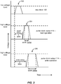
- Timing diagram 302 illustrates raw clock 122 at a low voltage level.
- output pulse clock 114 generated for a read operation is at a high voltage level and comprises a rising edge delay 304d; and as shown in timing diagram 306, output pulse clock 114 generated for a write operation is at a high voltage level and comprises a rising edge delay 306d.
- expected read array delay is accounted for (e.g. through read delay mimic logic 108 of Fig.
- rising edge delay 304d may be made as fast as required to meet the needs of a fast read operation. In comparison, rising edge delay 306d may not need to be fast and thus may be slowed down as required. Further, compared to timing diagram 304, timing diagram 306 illustrates pulse width 306w for a write operation to be wider than pulse width 304w for a read operation, in order to satisfy wider pulse width requirements of write operations as described above.
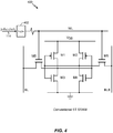
- output pulse clock 114 is used by logic components well known in the art, such as a word line decoder, generally designated by logic 402 in FIG. 4 .
- the operation of 6T SRAM cell 400 is well known.
- Transistors M1, M2, M3, and M4 form a crosscoupled inverter storage element, while access transistors M5 and M6 control read/write operations for the storage element.
- Word line WL controls the gates of access transistors M5 and M6, while complementary bit lines BL and BLB are used to select the particular 6T SRAM cell 400 for write operations and to read out the stored value for read operations.
- output pulse clock 114 may be applied to word line WL in order to meet specific pulse clock requirements for read and write operations, as shown, for example, in FIG. 3 .
- delays introduced by selective delay logic 102 may delay the rising edge of output pulse clock 114 during write operations, which again allows additional set up time for bit lines BL and BLB, and moreover may reduce power because accompanying buffers and drivers may be downsized. Further, the wider pulse width created by selective pulse width widening logic 110 may facilitate write operations even at lower voltage levels, which may lead to improved yield.
- pulse clock generation logic 112 may lead to lower latency and improved reuse of functional blocks, as compared to conventional implementations which have level shifters separated from pulse clock generation logic.
- the feedback path to built-in level shifter via pull-down transistors n3 and n4 may speed up the rising edge of output pulse clock 114 especially when the voltage difference between the low voltage level of raw clock 122 and the high voltage level of output pulse clock 114 is large.
- the latch mechanism in pulse clock generation logic 112 may additionally facilitate holding the logic state of output pulse clock 114 stable.
- an embodiment can include a method for generating a pulse clock (e.g. output pulse clock 114 of FIG. 1 ) comprising: configuring a programmable rising edge delay (e.g. rising edge delay 304d and 306d as illustrated in timing diagrams 304 and 306 of FIG. 3 ) of the pulse clock - Block 502; configuring a programmable pulse width (e.g. width 304w and 306w as illustrated in timing diagrams 304 and 306 of FIG. 3 ) of the pulse clock - Block 504; configuring a level shifter (e.g.
- a software module may reside in RAM memory, flash memory, ROM memory, EPROM memory, EEPROM memory, registers, hard disk, a removable disk, a CD-ROM, or any other form of storage medium known in the art.
- An exemplary storage medium is coupled to the processor such that the processor can read information from, and write information to, the storage medium. In the alternative, the storage medium may be integral to the processor.
- FIG. 6 a block diagram of a particular illustrative embodiment of a wireless device that includes a multi-core processor configured according to exemplary embodiments is depicted and generally designated 600.
- the device 600 includes a digital signal processor (DSP) 664, which may include self-timed pulse clock generation circuit 100 of FIG. 1 .
- DSP 664 may be coupled to memory 632 as shown, wherein the generated pulse clock from self-timed pulse clock generation circuit 100 may be used for memory accesses on memory 632.
- FIG. 6 also shows an external device such as display controller 626 that is coupled to DSP 664 and to display 628.
- An external device such as coder/decoder (CODEC) 634 (e.g., an audio and/or voice CODEC) can also be coupled to DSP 664.
- CODEC coder/decoder
- Other components/external devices, such as wireless controller 640 (which may include a modem) are also illustrated.
- Speaker 636 and microphone 638 can be coupled to CODEC 634.
- FIG. 6 also indicates that wireless controller 640 can be coupled to wireless antenna 642.
- DSP 664, display controller 626, memory 632, CODEC 634, and wireless controller 640 are included in a system-in-package or system-on-chip device 622.
- input device 630 and power supply 644 are coupled to the system-on-chip device 622.
- display 628, input device 630, speaker 636, microphone 638, wireless antenna 642, and power supply 644 are external to the system-on-chip device 622.
- each of display 628, input device 630, speaker 636, microphone 638, wireless antenna 642, and power supply 644 can be coupled to a component of the system-on-chip device 622, such as an interface or a controller.
- FIG. 6 depicts a wireless communications device
- DSP 664 and memory 632 may also be integrated into a set-top box, a music player, a video player, an entertainment unit, a navigation device, a personal digital assistant (PDA), a fixed location data unit, or a computer.
- a processor e.g., DSP 664 may also be integrated into such a device.
- an embodiment of the invention can include a computer readable media embodying a method for generating a pulse clock with a built-in level shifter and a programmable rising edge and programmable pulse width. Accordingly, the invention is not limited to illustrated examples and any means for performing the functionality described herein are included in embodiments of the invention.
Landscapes
- Engineering & Computer Science (AREA)
- Microelectronics & Electronic Packaging (AREA)
- Computer Hardware Design (AREA)
- Theoretical Computer Science (AREA)
- Physics & Mathematics (AREA)
- General Engineering & Computer Science (AREA)
- General Physics & Mathematics (AREA)
- Pulse Circuits (AREA)
Applications Claiming Priority (2)
| Application Number | Priority Date | Filing Date | Title |
|---|---|---|---|
| US13/433,891 US8638153B2 (en) | 2012-03-29 | 2012-03-29 | Pulse clock generation logic with built-in level shifter and programmable rising edge and pulse width |
| PCT/US2013/034414 WO2013149040A1 (en) | 2012-03-29 | 2013-03-28 | A pulse clock generation logic with built-in level shifter and programmable rising edge and pulse width |
Publications (2)
| Publication Number | Publication Date |
|---|---|
| EP2831694A1 EP2831694A1 (en) | 2015-02-04 |
| EP2831694B1 true EP2831694B1 (en) | 2017-08-23 |
Family
ID=48083683
Family Applications (1)
| Application Number | Title | Priority Date | Filing Date |
|---|---|---|---|
| EP13715579.2A Not-in-force EP2831694B1 (en) | 2012-03-29 | 2013-03-28 | A pulse clock generation logic with built-in level shifter and programmable rising edge and pulse width |
Country Status (6)
| Country | Link |
|---|---|
| US (1) | US8638153B2 (enExample) |
| EP (1) | EP2831694B1 (enExample) |
| JP (1) | JP6242852B2 (enExample) |
| KR (1) | KR20140139595A (enExample) |
| CN (1) | CN104204992B (enExample) |
| WO (1) | WO2013149040A1 (enExample) |
Families Citing this family (17)
| Publication number | Priority date | Publication date | Assignee | Title |
|---|---|---|---|---|
| BR122016006764B1 (pt) | 2013-03-15 | 2022-02-01 | Intel Corporation | Aparelhos e métodos de memória |
| CN104680991B (zh) * | 2015-03-03 | 2017-03-08 | 深圳市华星光电技术有限公司 | 用于goa架构液晶面板的电平移位电路及电平移位方法 |
| KR102295058B1 (ko) | 2015-08-19 | 2021-08-31 | 삼성전자주식회사 | 반도체 메모리 시스템 및 반도체 메모리 장치 및 반도체 메모리 장치의 동작방법 |
| US9564901B1 (en) | 2015-12-17 | 2017-02-07 | Apple Inc. | Self-timed dynamic level shifter with falling edge generator |
| CN106940423B (zh) * | 2016-01-05 | 2023-02-24 | 华润微集成电路(无锡)有限公司 | 多功能芯片内置的测试电路 |
| US9607674B1 (en) * | 2016-01-06 | 2017-03-28 | Qualcomm Incorporated | Pulse latch reset tracking at high differential voltage |
| US10163508B2 (en) | 2016-02-26 | 2018-12-25 | Intel Corporation | Supporting multiple memory types in a memory slot |
| US10615796B2 (en) * | 2016-07-29 | 2020-04-07 | Qualcomm Incorporated | Level shifter |
| US10163474B2 (en) * | 2016-09-22 | 2018-12-25 | Qualcomm Incorporated | Apparatus and method of clock shaping for memory |
| US9990984B1 (en) | 2016-12-06 | 2018-06-05 | Qualcomm Incorporated | Pulse-stretcher clock generator circuit for high speed memory subsystems |
| CN106941347B (zh) * | 2017-03-17 | 2019-08-06 | 中国电子科技集团公司第二十四研究所 | 占空比调节装置及方法 |
| US10389335B1 (en) | 2018-05-04 | 2019-08-20 | Apple Inc. | Clock pulse generation circuit |
| US10790826B1 (en) * | 2019-05-19 | 2020-09-29 | Novatek Microelectronics Corp. | Level shifter with low power consumption |
| US11972834B2 (en) * | 2019-11-11 | 2024-04-30 | Qualcomm Incorporated | Low power and robust level-shifting pulse latch for dual-power memories |
| CN114006605B (zh) * | 2021-12-31 | 2022-05-10 | 峰岹科技(深圳)股份有限公司 | 单边沿延时电路 |
| US12340864B2 (en) * | 2022-02-11 | 2025-06-24 | Synopsys, Inc. | Interface level-shifter dual-rail memory architecture |
| CN118538263A (zh) * | 2024-07-25 | 2024-08-23 | 中科亿海微电子科技(苏州)有限公司 | 一种对fpga bram读写冲突的时序控制方法及电路 |
Family Cites Families (13)
| Publication number | Priority date | Publication date | Assignee | Title |
|---|---|---|---|---|
| US5027323A (en) | 1988-01-14 | 1991-06-25 | Hitachi, Ltd. | Write pulse signal generating circuit for a semiconductor memory device |
| US6072348A (en) * | 1997-07-09 | 2000-06-06 | Xilinx, Inc. | Programmable power reduction in a clock-distribution circuit |
| US5929684A (en) * | 1998-03-06 | 1999-07-27 | Siemens Aktiengesellschaft | Feedback pulse generators |
| JP2003030991A (ja) * | 2001-07-12 | 2003-01-31 | Sanyo Electric Co Ltd | メモリ |
| CN2544466Y (zh) * | 2002-01-25 | 2003-04-09 | 威盛电子股份有限公司 | 无突波干扰的时钟脉冲输出电路 |
| US6975154B1 (en) * | 2003-04-29 | 2005-12-13 | Altera Corporation | Reduced power consumption clock network |
| JP4173887B2 (ja) * | 2003-08-13 | 2008-10-29 | 富士通株式会社 | パルス生成回路 |
| US6850460B1 (en) | 2004-05-12 | 2005-02-01 | International Business Machines Corporation | High performance programmable array local clock generator |
| US7180353B2 (en) | 2005-02-03 | 2007-02-20 | Mediatek Incorporation | Apparatus and method for low power clock distribution |
| US7609583B2 (en) | 2007-11-12 | 2009-10-27 | Micron Technology, Inc. | Selective edge phase mixing |
| US7876631B2 (en) * | 2008-12-17 | 2011-01-25 | Qualcomm Incorporated | Self-tuning of signal path delay in circuit employing multiple voltage domains |
| US8102720B2 (en) | 2009-02-02 | 2012-01-24 | Qualcomm Incorporated | System and method of pulse generation |
| CN101847991B (zh) * | 2009-03-27 | 2012-01-11 | 台湾积体电路制造股份有限公司 | 时钟脉冲产生器、存储器电路及产生内部时钟脉冲信号的方法 |
-
2012
- 2012-03-29 US US13/433,891 patent/US8638153B2/en not_active Expired - Fee Related
-
2013
- 2013-03-28 JP JP2015503586A patent/JP6242852B2/ja not_active Expired - Fee Related
- 2013-03-28 WO PCT/US2013/034414 patent/WO2013149040A1/en not_active Ceased
- 2013-03-28 EP EP13715579.2A patent/EP2831694B1/en not_active Not-in-force
- 2013-03-28 KR KR1020147029964A patent/KR20140139595A/ko not_active Withdrawn
- 2013-03-28 CN CN201380016930.XA patent/CN104204992B/zh not_active Expired - Fee Related
Non-Patent Citations (1)
| Title |
|---|
| None * |
Also Published As
| Publication number | Publication date |
|---|---|
| CN104204992B (zh) | 2017-05-17 |
| JP6242852B2 (ja) | 2017-12-06 |
| US8638153B2 (en) | 2014-01-28 |
| WO2013149040A1 (en) | 2013-10-03 |
| EP2831694A1 (en) | 2015-02-04 |
| CN104204992A (zh) | 2014-12-10 |
| KR20140139595A (ko) | 2014-12-05 |
| JP2015520434A (ja) | 2015-07-16 |
| US20130257498A1 (en) | 2013-10-03 |
Similar Documents
| Publication | Publication Date | Title |
|---|---|---|
| EP2831694B1 (en) | A pulse clock generation logic with built-in level shifter and programmable rising edge and pulse width | |
| US10461747B2 (en) | Low power clock gating circuit | |
| CN109074332B (zh) | 用于控制输入信号路径上的等待时间的设备 | |
| JP5055448B2 (ja) | ディレイロックループのディレイロック状態の情報の使用が可能な半導体素子 | |
| KR101018706B1 (ko) | 반도체 메모리 장치 및 그 구동방법 | |
| US8994402B2 (en) | Level shifter circuit optimized for metastability resolution and integrated level shifter and metastability resolution circuit | |
| US9036446B2 (en) | Global reset with replica for pulse latch pre-decoders | |
| JP5282560B2 (ja) | 半導体装置及びシステム | |
| EP2951943B1 (en) | Rotational synchronizer circuit for metastablity resolution | |
| EP3198609B1 (en) | Voltage level shifted self-clocked write assistance | |
| US9196330B2 (en) | Mimicking multi-voltage domain wordline decoding logic for a memory array | |
| US10026472B2 (en) | Multi-port memory and semiconductor device | |
| KR102293806B1 (ko) | 메모리 판독 액세스들 동안 전력 글리치들을 감소시키기 위한 정적 랜덤 액세스 메모리(sram) 글로벌 비트라인 회로들 및 관련 방법들 및 시스템들 | |
| US7714632B2 (en) | Clock control circuit and semiconductor integrated circuit using the same | |
| CN102664609B (zh) | 自适应感应设计 | |
| JP2002304887A (ja) | 半導体集積回路 | |
| US20190089337A1 (en) | Flop Circuit with Integrated Clock Gating Circuit | |
| US9911472B1 (en) | Write bitline driver for a dual voltage domain | |
| CN112154606B (zh) | 具有嵌入式逻辑的电平转换锁存器的方法、装置和系统 | |
| US20180152176A1 (en) | Voltage aware circuit for dual voltage domain signals | |
| KR100712986B1 (ko) | 래치회로 | |
| KR101819134B1 (ko) | 반도체 메모리 장치 | |
| US20100165781A1 (en) | Internal write/read pulse generating circuit of a semiconductor memory apparatus | |
| JP2014078313A (ja) | 半導体装置 |
Legal Events
| Date | Code | Title | Description |
|---|---|---|---|
| PUAI | Public reference made under article 153(3) epc to a published international application that has entered the european phase |
Free format text: ORIGINAL CODE: 0009012 |
|
| 17P | Request for examination filed |
Effective date: 20140910 |
|
| AK | Designated contracting states |
Kind code of ref document: A1 Designated state(s): AL AT BE BG CH CY CZ DE DK EE ES FI FR GB GR HR HU IE IS IT LI LT LU LV MC MK MT NL NO PL PT RO RS SE SI SK SM TR |
|
| AX | Request for extension of the european patent |
Extension state: BA ME |
|
| DAX | Request for extension of the european patent (deleted) | ||
| REG | Reference to a national code |
Ref country code: DE Ref legal event code: R079 Ref document number: 602013025418 Country of ref document: DE Free format text: PREVIOUS MAIN CLASS: G06F0001040000 Ipc: G11C0011417000 |
|
| RIC1 | Information provided on ipc code assigned before grant |
Ipc: G11C 11/417 20060101AFI20170228BHEP Ipc: G11C 11/418 20060101ALI20170228BHEP Ipc: G06F 1/04 20060101ALI20170228BHEP Ipc: G11C 11/419 20060101ALI20170228BHEP Ipc: G11C 7/22 20060101ALI20170228BHEP |
|
| GRAP | Despatch of communication of intention to grant a patent |
Free format text: ORIGINAL CODE: EPIDOSNIGR1 |
|
| INTG | Intention to grant announced |
Effective date: 20170410 |
|
| GRAS | Grant fee paid |
Free format text: ORIGINAL CODE: EPIDOSNIGR3 |
|
| GRAA | (expected) grant |
Free format text: ORIGINAL CODE: 0009210 |
|
| AK | Designated contracting states |
Kind code of ref document: B1 Designated state(s): AL AT BE BG CH CY CZ DE DK EE ES FI FR GB GR HR HU IE IS IT LI LT LU LV MC MK MT NL NO PL PT RO RS SE SI SK SM TR |
|
| REG | Reference to a national code |
Ref country code: GB Ref legal event code: FG4D |
|
| REG | Reference to a national code |
Ref country code: CH Ref legal event code: EP |
|
| REG | Reference to a national code |
Ref country code: AT Ref legal event code: REF Ref document number: 922144 Country of ref document: AT Kind code of ref document: T Effective date: 20170915 |
|
| REG | Reference to a national code |
Ref country code: IE Ref legal event code: FG4D |
|
| REG | Reference to a national code |
Ref country code: DE Ref legal event code: R096 Ref document number: 602013025418 Country of ref document: DE |
|
| REG | Reference to a national code |
Ref country code: NL Ref legal event code: MP Effective date: 20170823 |
|
| REG | Reference to a national code |
Ref country code: LT Ref legal event code: MG4D |
|
| REG | Reference to a national code |
Ref country code: AT Ref legal event code: MK05 Ref document number: 922144 Country of ref document: AT Kind code of ref document: T Effective date: 20170823 |
|
| PG25 | Lapsed in a contracting state [announced via postgrant information from national office to epo] |
Ref country code: LT Free format text: LAPSE BECAUSE OF FAILURE TO SUBMIT A TRANSLATION OF THE DESCRIPTION OR TO PAY THE FEE WITHIN THE PRESCRIBED TIME-LIMIT Effective date: 20170823 Ref country code: SE Free format text: LAPSE BECAUSE OF FAILURE TO SUBMIT A TRANSLATION OF THE DESCRIPTION OR TO PAY THE FEE WITHIN THE PRESCRIBED TIME-LIMIT Effective date: 20170823 Ref country code: AT Free format text: LAPSE BECAUSE OF FAILURE TO SUBMIT A TRANSLATION OF THE DESCRIPTION OR TO PAY THE FEE WITHIN THE PRESCRIBED TIME-LIMIT Effective date: 20170823 Ref country code: NL Free format text: LAPSE BECAUSE OF FAILURE TO SUBMIT A TRANSLATION OF THE DESCRIPTION OR TO PAY THE FEE WITHIN THE PRESCRIBED TIME-LIMIT Effective date: 20170823 Ref country code: NO Free format text: LAPSE BECAUSE OF FAILURE TO SUBMIT A TRANSLATION OF THE DESCRIPTION OR TO PAY THE FEE WITHIN THE PRESCRIBED TIME-LIMIT Effective date: 20171123 Ref country code: HR Free format text: LAPSE BECAUSE OF FAILURE TO SUBMIT A TRANSLATION OF THE DESCRIPTION OR TO PAY THE FEE WITHIN THE PRESCRIBED TIME-LIMIT Effective date: 20170823 Ref country code: FI Free format text: LAPSE BECAUSE OF FAILURE TO SUBMIT A TRANSLATION OF THE DESCRIPTION OR TO PAY THE FEE WITHIN THE PRESCRIBED TIME-LIMIT Effective date: 20170823 |
|
| REG | Reference to a national code |
Ref country code: FR Ref legal event code: PLFP Year of fee payment: 6 |
|
| PG25 | Lapsed in a contracting state [announced via postgrant information from national office to epo] |
Ref country code: GR Free format text: LAPSE BECAUSE OF FAILURE TO SUBMIT A TRANSLATION OF THE DESCRIPTION OR TO PAY THE FEE WITHIN THE PRESCRIBED TIME-LIMIT Effective date: 20171124 Ref country code: PL Free format text: LAPSE BECAUSE OF FAILURE TO SUBMIT A TRANSLATION OF THE DESCRIPTION OR TO PAY THE FEE WITHIN THE PRESCRIBED TIME-LIMIT Effective date: 20170823 Ref country code: RS Free format text: LAPSE BECAUSE OF FAILURE TO SUBMIT A TRANSLATION OF THE DESCRIPTION OR TO PAY THE FEE WITHIN THE PRESCRIBED TIME-LIMIT Effective date: 20170823 Ref country code: IS Free format text: LAPSE BECAUSE OF FAILURE TO SUBMIT A TRANSLATION OF THE DESCRIPTION OR TO PAY THE FEE WITHIN THE PRESCRIBED TIME-LIMIT Effective date: 20171223 Ref country code: BG Free format text: LAPSE BECAUSE OF FAILURE TO SUBMIT A TRANSLATION OF THE DESCRIPTION OR TO PAY THE FEE WITHIN THE PRESCRIBED TIME-LIMIT Effective date: 20171123 Ref country code: LV Free format text: LAPSE BECAUSE OF FAILURE TO SUBMIT A TRANSLATION OF THE DESCRIPTION OR TO PAY THE FEE WITHIN THE PRESCRIBED TIME-LIMIT Effective date: 20170823 Ref country code: ES Free format text: LAPSE BECAUSE OF FAILURE TO SUBMIT A TRANSLATION OF THE DESCRIPTION OR TO PAY THE FEE WITHIN THE PRESCRIBED TIME-LIMIT Effective date: 20170823 |
|
| PG25 | Lapsed in a contracting state [announced via postgrant information from national office to epo] |
Ref country code: DK Free format text: LAPSE BECAUSE OF FAILURE TO SUBMIT A TRANSLATION OF THE DESCRIPTION OR TO PAY THE FEE WITHIN THE PRESCRIBED TIME-LIMIT Effective date: 20170823 Ref country code: RO Free format text: LAPSE BECAUSE OF FAILURE TO SUBMIT A TRANSLATION OF THE DESCRIPTION OR TO PAY THE FEE WITHIN THE PRESCRIBED TIME-LIMIT Effective date: 20170823 Ref country code: CZ Free format text: LAPSE BECAUSE OF FAILURE TO SUBMIT A TRANSLATION OF THE DESCRIPTION OR TO PAY THE FEE WITHIN THE PRESCRIBED TIME-LIMIT Effective date: 20170823 |
|
| PGFP | Annual fee paid to national office [announced via postgrant information from national office to epo] |
Ref country code: GB Payment date: 20180223 Year of fee payment: 6 |
|
| REG | Reference to a national code |
Ref country code: DE Ref legal event code: R097 Ref document number: 602013025418 Country of ref document: DE |
|
| PG25 | Lapsed in a contracting state [announced via postgrant information from national office to epo] |
Ref country code: SM Free format text: LAPSE BECAUSE OF FAILURE TO SUBMIT A TRANSLATION OF THE DESCRIPTION OR TO PAY THE FEE WITHIN THE PRESCRIBED TIME-LIMIT Effective date: 20170823 Ref country code: SK Free format text: LAPSE BECAUSE OF FAILURE TO SUBMIT A TRANSLATION OF THE DESCRIPTION OR TO PAY THE FEE WITHIN THE PRESCRIBED TIME-LIMIT Effective date: 20170823 Ref country code: EE Free format text: LAPSE BECAUSE OF FAILURE TO SUBMIT A TRANSLATION OF THE DESCRIPTION OR TO PAY THE FEE WITHIN THE PRESCRIBED TIME-LIMIT Effective date: 20170823 Ref country code: IT Free format text: LAPSE BECAUSE OF FAILURE TO SUBMIT A TRANSLATION OF THE DESCRIPTION OR TO PAY THE FEE WITHIN THE PRESCRIBED TIME-LIMIT Effective date: 20170823 |
|
| PGFP | Annual fee paid to national office [announced via postgrant information from national office to epo] |
Ref country code: FR Payment date: 20180223 Year of fee payment: 6 |
|
| PLBE | No opposition filed within time limit |
Free format text: ORIGINAL CODE: 0009261 |
|
| STAA | Information on the status of an ep patent application or granted ep patent |
Free format text: STATUS: NO OPPOSITION FILED WITHIN TIME LIMIT |
|
| 26N | No opposition filed |
Effective date: 20180524 |
|
| PG25 | Lapsed in a contracting state [announced via postgrant information from national office to epo] |
Ref country code: SI Free format text: LAPSE BECAUSE OF FAILURE TO SUBMIT A TRANSLATION OF THE DESCRIPTION OR TO PAY THE FEE WITHIN THE PRESCRIBED TIME-LIMIT Effective date: 20170823 |
|
| REG | Reference to a national code |
Ref country code: CH Ref legal event code: PL |
|
| PG25 | Lapsed in a contracting state [announced via postgrant information from national office to epo] |
Ref country code: MC Free format text: LAPSE BECAUSE OF FAILURE TO SUBMIT A TRANSLATION OF THE DESCRIPTION OR TO PAY THE FEE WITHIN THE PRESCRIBED TIME-LIMIT Effective date: 20170823 |
|
| REG | Reference to a national code |
Ref country code: BE Ref legal event code: MM Effective date: 20180331 |
|
| REG | Reference to a national code |
Ref country code: IE Ref legal event code: MM4A |
|
| PG25 | Lapsed in a contracting state [announced via postgrant information from national office to epo] |
Ref country code: LU Free format text: LAPSE BECAUSE OF NON-PAYMENT OF DUE FEES Effective date: 20180328 |
|
| PG25 | Lapsed in a contracting state [announced via postgrant information from national office to epo] |
Ref country code: IE Free format text: LAPSE BECAUSE OF NON-PAYMENT OF DUE FEES Effective date: 20180328 |
|
| PG25 | Lapsed in a contracting state [announced via postgrant information from national office to epo] |
Ref country code: CH Free format text: LAPSE BECAUSE OF NON-PAYMENT OF DUE FEES Effective date: 20180331 Ref country code: LI Free format text: LAPSE BECAUSE OF NON-PAYMENT OF DUE FEES Effective date: 20180331 Ref country code: BE Free format text: LAPSE BECAUSE OF NON-PAYMENT OF DUE FEES Effective date: 20180331 |
|
| GBPC | Gb: european patent ceased through non-payment of renewal fee |
Effective date: 20190328 |
|
| PG25 | Lapsed in a contracting state [announced via postgrant information from national office to epo] |
Ref country code: MT Free format text: LAPSE BECAUSE OF NON-PAYMENT OF DUE FEES Effective date: 20180328 Ref country code: GB Free format text: LAPSE BECAUSE OF NON-PAYMENT OF DUE FEES Effective date: 20190328 |
|
| PG25 | Lapsed in a contracting state [announced via postgrant information from national office to epo] |
Ref country code: FR Free format text: LAPSE BECAUSE OF NON-PAYMENT OF DUE FEES Effective date: 20190331 |
|
| PG25 | Lapsed in a contracting state [announced via postgrant information from national office to epo] |
Ref country code: TR Free format text: LAPSE BECAUSE OF FAILURE TO SUBMIT A TRANSLATION OF THE DESCRIPTION OR TO PAY THE FEE WITHIN THE PRESCRIBED TIME-LIMIT Effective date: 20170823 |
|
| PG25 | Lapsed in a contracting state [announced via postgrant information from national office to epo] |
Ref country code: PT Free format text: LAPSE BECAUSE OF FAILURE TO SUBMIT A TRANSLATION OF THE DESCRIPTION OR TO PAY THE FEE WITHIN THE PRESCRIBED TIME-LIMIT Effective date: 20170823 |
|
| PG25 | Lapsed in a contracting state [announced via postgrant information from national office to epo] |
Ref country code: MK Free format text: LAPSE BECAUSE OF NON-PAYMENT OF DUE FEES Effective date: 20170823 Ref country code: CY Free format text: LAPSE BECAUSE OF FAILURE TO SUBMIT A TRANSLATION OF THE DESCRIPTION OR TO PAY THE FEE WITHIN THE PRESCRIBED TIME-LIMIT Effective date: 20170823 Ref country code: HU Free format text: LAPSE BECAUSE OF FAILURE TO SUBMIT A TRANSLATION OF THE DESCRIPTION OR TO PAY THE FEE WITHIN THE PRESCRIBED TIME-LIMIT; INVALID AB INITIO Effective date: 20130328 |
|
| PG25 | Lapsed in a contracting state [announced via postgrant information from national office to epo] |
Ref country code: AL Free format text: LAPSE BECAUSE OF FAILURE TO SUBMIT A TRANSLATION OF THE DESCRIPTION OR TO PAY THE FEE WITHIN THE PRESCRIBED TIME-LIMIT Effective date: 20170823 |
|
| PGFP | Annual fee paid to national office [announced via postgrant information from national office to epo] |
Ref country code: DE Payment date: 20210210 Year of fee payment: 9 |
|
| REG | Reference to a national code |
Ref country code: DE Ref legal event code: R119 Ref document number: 602013025418 Country of ref document: DE |
|
| PG25 | Lapsed in a contracting state [announced via postgrant information from national office to epo] |
Ref country code: DE Free format text: LAPSE BECAUSE OF NON-PAYMENT OF DUE FEES Effective date: 20221001 |