EP2831694B1 - A pulse clock generation logic with built-in level shifter and programmable rising edge and pulse width - Google Patents
A pulse clock generation logic with built-in level shifter and programmable rising edge and pulse width Download PDFInfo
- Publication number
- EP2831694B1 EP2831694B1 EP13715579.2A EP13715579A EP2831694B1 EP 2831694 B1 EP2831694 B1 EP 2831694B1 EP 13715579 A EP13715579 A EP 13715579A EP 2831694 B1 EP2831694 B1 EP 2831694B1
- Authority
- EP
- European Patent Office
- Prior art keywords
- pulse clock
- pulse
- delay
- logic
- clock generation
- Prior art date
- Legal status (The legal status is an assumption and is not a legal conclusion. Google has not performed a legal analysis and makes no representation as to the accuracy of the status listed.)
- Not-in-force
Links
- 230000000630 rising effect Effects 0.000 title claims description 44
- 238000000034 method Methods 0.000 claims description 23
- 230000003111 delayed effect Effects 0.000 claims description 22
- 230000003278 mimic effect Effects 0.000 claims description 14
- 230000006399 behavior Effects 0.000 claims 2
- 238000004590 computer program Methods 0.000 claims 1
- 238000010586 diagram Methods 0.000 description 10
- 230000001934 delay Effects 0.000 description 8
- 230000009471 action Effects 0.000 description 5
- 230000007246 mechanism Effects 0.000 description 5
- 230000008569 process Effects 0.000 description 5
- 239000000872 buffer Substances 0.000 description 4
- HCUOEKSZWPGJIM-YBRHCDHNSA-N (e,2e)-2-hydroxyimino-6-methoxy-4-methyl-5-nitrohex-3-enamide Chemical compound COCC([N+]([O-])=O)\C(C)=C\C(=N/O)\C(N)=O HCUOEKSZWPGJIM-YBRHCDHNSA-N 0.000 description 3
- 101100162200 Aspergillus parasiticus (strain ATCC 56775 / NRRL 5862 / SRRC 143 / SU-1) aflD gene Proteins 0.000 description 3
- 230000006870 function Effects 0.000 description 3
- 230000008901 benefit Effects 0.000 description 2
- 238000004891 communication Methods 0.000 description 2
- 239000002245 particle Substances 0.000 description 2
- 238000003491 array Methods 0.000 description 1
- 230000008859 change Effects 0.000 description 1
- 230000000295 complement effect Effects 0.000 description 1
- 239000013078 crystal Substances 0.000 description 1
- 238000013461 design Methods 0.000 description 1
- 230000000694 effects Effects 0.000 description 1
- 238000005516 engineering process Methods 0.000 description 1
- 238000012986 modification Methods 0.000 description 1
- 230000004048 modification Effects 0.000 description 1
- 230000003287 optical effect Effects 0.000 description 1
- 238000012545 processing Methods 0.000 description 1
- 230000003068 static effect Effects 0.000 description 1
Images

Classifications
-
- G—PHYSICS
- G06—COMPUTING; CALCULATING OR COUNTING
- G06F—ELECTRIC DIGITAL DATA PROCESSING
- G06F1/00—Details not covered by groups G06F3/00 - G06F13/00 and G06F21/00
- G06F1/04—Generating or distributing clock signals or signals derived directly therefrom
-
- G—PHYSICS
- G11—INFORMATION STORAGE
- G11C—STATIC STORES
- G11C11/00—Digital stores characterised by the use of particular electric or magnetic storage elements; Storage elements therefor
- G11C11/21—Digital stores characterised by the use of particular electric or magnetic storage elements; Storage elements therefor using electric elements
- G11C11/34—Digital stores characterised by the use of particular electric or magnetic storage elements; Storage elements therefor using electric elements using semiconductor devices
- G11C11/40—Digital stores characterised by the use of particular electric or magnetic storage elements; Storage elements therefor using electric elements using semiconductor devices using transistors
- G11C11/41—Digital stores characterised by the use of particular electric or magnetic storage elements; Storage elements therefor using electric elements using semiconductor devices using transistors forming static cells with positive feedback, i.e. cells not needing refreshing or charge regeneration, e.g. bistable multivibrator or Schmitt trigger
- G11C11/413—Auxiliary circuits, e.g. for addressing, decoding, driving, writing, sensing, timing or power reduction
- G11C11/417—Auxiliary circuits, e.g. for addressing, decoding, driving, writing, sensing, timing or power reduction for memory cells of the field-effect type
- G11C11/418—Address circuits
-
- G—PHYSICS
- G11—INFORMATION STORAGE
- G11C—STATIC STORES
- G11C11/00—Digital stores characterised by the use of particular electric or magnetic storage elements; Storage elements therefor
- G11C11/21—Digital stores characterised by the use of particular electric or magnetic storage elements; Storage elements therefor using electric elements
- G11C11/34—Digital stores characterised by the use of particular electric or magnetic storage elements; Storage elements therefor using electric elements using semiconductor devices
- G11C11/40—Digital stores characterised by the use of particular electric or magnetic storage elements; Storage elements therefor using electric elements using semiconductor devices using transistors
- G11C11/41—Digital stores characterised by the use of particular electric or magnetic storage elements; Storage elements therefor using electric elements using semiconductor devices using transistors forming static cells with positive feedback, i.e. cells not needing refreshing or charge regeneration, e.g. bistable multivibrator or Schmitt trigger
- G11C11/413—Auxiliary circuits, e.g. for addressing, decoding, driving, writing, sensing, timing or power reduction
- G11C11/417—Auxiliary circuits, e.g. for addressing, decoding, driving, writing, sensing, timing or power reduction for memory cells of the field-effect type
- G11C11/419—Read-write [R-W] circuits
-
- G—PHYSICS
- G11—INFORMATION STORAGE
- G11C—STATIC STORES
- G11C7/00—Arrangements for writing information into, or reading information out from, a digital store
- G11C7/22—Read-write [R-W] timing or clocking circuits; Read-write [R-W] control signal generators or management
- G11C7/222—Clock generating, synchronizing or distributing circuits within memory device
Definitions
- Disclosed embodiments generally relate to pulse clock generation. More particularly, exemplary embodiments are directed to generating pulse clocks with programmable edges and pulse widths configured for varying requirements of different memory access operations.
- T-SRAM 6 Transistor Static Random Access Memory
- 6T-SRAM 6 Transistor Static Random Access Memory
- a common solution involves the use of multiple voltage domains, such that memory cells may be operated at a relatively high voltage level while other on-chip logic may be operated at lower voltages.
- level shifters are commonly used to convert low voltage to high voltage and vice versa as needed.
- level shifters introduce latency, which may be undesirable in timing critical paths.
- Document US6850460 discloses a SRAM array local clock generator having variable delay settings that are programmable via level scan bits. Program bits from the level scan operation are decoded and used to adjust the number of delay elements in the local clock generator path.
- pulse clocks are often utilized to overcome the effects of device variations (e.g. due to process variations). These pulse clocks may be subjected to conflicting needs for different memory access operations. For example, during a memory read operation it may be desirable for the rising edge of the pulse clock to arrive as fast as possible at memory cells of the memory array being accessed, in order to enable quick read access. Moreover, during the memory read operation it may be desirable for the pulse width of the pulse clock to be narrow, in order to reduce power consumption by disallowing full voltage swings on bit lines.
- memory write operations are usually not timing critical, and thus can tolerate higher arrival delays in the rising edge of the pulse clock.
- memory write operations may benefit from delays in the pulse clock so as to allow sufficient set-up time for the data written.
- the pulse width of the pulse clock may be wider to allow for sufficient write time in order to guarantee successful completion of the write operations, especially at lower supply voltage levels.
- Conventional pulse clock implementations are not well suited to meet these conflicting needs for read and write operations on memory cells.
- Exemplary embodiments of the invention are directed to circuits and methods for generating pulse clocks with programmable edges and pulse widths configured for varying requirements of different memory access operations.
- an exemplary embodiment is directed to a method for generating a pulse clock comprising: configuring a programmable rising edge delay of the pulse clock; configuring a programmable pulse width of the pulse clock; configuring a level shifter for shifting a voltage level of the pulse clock; and generating the pulse clock in accordance with the programmed rising edge delay, programmed pulse width, and shifted voltage level.
- Another exemplary embodiment is directed to a pulse clock generation circuit comprising: a selective delay logic to provide a programmable rising edge delay of the pulse clock; a selective pulse width widening logic to provide a programmable pulse width of the pulse clock; a built-in level shifter configured to shift a voltage level of the pulse clock; and logic configured to generate the pulse clock in accordance with the programmed rising edge delay, programmed pulse width, and shifted voltage level.
- Yet another exemplary embodiment is directed to non-transitory computer-readable storage medium comprising code, which, when executed by a processor, causes the processor to perform operations for programming a pulse clock generator, the non-transitory computer-readable storage medium comprising: code for configuring a programmable rising edge delay of the pulse clock; code for configuring a programmable pulse width of the pulse clock; code for configuring a level shifter for shifting a voltage level of the pulse clock; and code for generating the pulse clock in accordance with the programmed rising edge delay, programmed pulse width, and shifted voltage level.
- Exemplary embodiments are directed to self-timed pulse clock generation circuits configured for programmable pulse width and rising edge delays in order to meet conflicting requirements of read and write operations. Further, exemplary embodiments may include a built-in level shifter configured to convert a raw clock in a low voltage domain to pulse clocks for read and write operations in high voltage domain without introducing additional delays from a separate voltage level shifter, while also preventing glitches and charge sharing problems which may occur in conventional implementations.
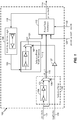
- Raw clock 122 may be input to self-timed pulse clock generation circuit 100, and may serve as a base clock for generating customized clock pulses for read and write operations.
- Raw clock 122 may be generated by known techniques such as by the use of piezoelectric crystals, etc.
- Raw clock 122 may be made available at a low voltage level or may be derived from a low voltage domain.
- Raw clock 122 may first enter selective delay logic 102, wherein raw clock 122 may be delayed selectively for write operations.
- Programmable delay logic 104, read/write control 126 and selector 106 may be configured as shown for selectively delaying raw clock 122. In one example, if a read operation is indicated by read/write control 126, then raw clock 122 may be selected by selector 106 to form the selectively delayed output clock clk_d1 116. On the other hand, if read/write control 126 indicates a write operation, then programmable delay logic 104 may delay raw clock 122 by a desired amount and generate a delayed clock 124, which may then be selected by selector 106 to form the selectively delayed output clock clk_d1 116.
- Programmable delay logic 104 may be implemented by known techniques, such as, by controlling a number of inverters or buffer elements to be coupled in series. Effective sizes of these inverters or buffer elements may also be controlled to adjust the delay amount. Skilled persons will recognize suitable implementations for programmable delay logic 104.
- Pulse clock generation logic 112 may ultimately output pulse clock 114 which meets above-noted requirements for read and write operations in exemplary embodiments.
- Pulse clock generation logic 112 may include logic for voltage level shifting, such that output pulse clock 114 is made available at a high voltage level without introducing unwanted latency from a separate voltage level shifter. Further, pulse clock generation logic 112 may be configured to eliminate glitches in output pulse clock 114.
- Feedback path 118 from output pulse clock 114 back to pulse clock generation logic 112 through reset 121 may include read delay mimic logic 108 and selective pulse width widening logic 110 as shown. Feedback path 118 may provide a self-resetting and thus self-timing functionality to pulse clock generation logic 112. Pulse clock generation logic 112, read delay mimic logic 108, and selective pulse width widening logic 110 will now be described in further detail.
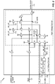
- pulse clock generation logic 112 includes a transistor-level schematic.
- Enable 130 and power-up reset 128 are input to clock generation logic 112 from an external source (not shown) to enable or reset the output pulse clock 114.
- An exemplary operation of pulse clock generation logic 112 will now be described. Initially, power-up reset 128 is driven high, thus causing the output of inverter i6 to be driven low and triggering pull-up transistor p3 to pull up lat_node 142 and thereby driving output pulse clock 114 low via inverter i5. It will be observed that pull-up transistor p3 is in the high voltage domain, as indicated in FIG. 2 . Thus, output pulse clock 114 is derived in the high voltage domain.
- a first instance of a rising edge of raw clock 122 will now be considered. It will be recalled that the selectively delayed output clock clk_d1 116 is a selectively delayed version of raw clock 122. Both raw clock 122 and selectively delayed output clock clk_d1 116 may be in the low voltage domain. Thus, a rising edge of raw clock 122 may cause a rising edge of selectively delayed output clock clk_d1 116 after a delay, and then turn on pull-down transistor n1. At this instance in time pull-down transistor n3 will remain turned off. It will be noticed from FIG.
- pull-up transistors p5 and p6 will be partially turned off, because the source voltages of pull-up transistors p5 and p6 are in the high voltage domain and their gate voltages are in the low voltage domain; and all four pull-down transistors n0, n1, n2, and n4 will be turned on at this instance. Therefore, both nodes int_node 144 and lat_node 142 will be pulled down and inverter i5 will drive output pulse clock 114 high.
- pull-down transistor n3 will be turned on, which will provide additional current source to speed up the pull down process of lat_node 142 and int_node 144 .
- output pulse clock 114 is already in the high voltage domain. Accordingly, the rising edge of raw clock 122 in the low voltage domain creates a rising edge of output pulse clock 114 in the high voltage domain without requiring additional voltage level shifting logic. While pull-up transistors p5 and p6 being turned off halfway may incur minor delay and power consumption costs, these costs may be offset by the additional pull-down path provided by pull-down transistors n3 and n4.
- lat_node 142 will remain in the low state and pulse clock 114 will remain in the high state due to the latch created by inverter i4 and the combination of pull-up transistors p4, p6 and pull-down transistors n3, n4, until a reset mechanism returns lat_node 142 to high state, thus driving output pulse clock 114 low.
- Reset 121 which will be described in further detail below, can control the falling edge of output pulse clock 114. It will be recognized that controlling the time period between the rising edge of output pulse clock 114 and the falling edge of output pulse clock 114 will determine the width of the clock pulse derived at output pulse clock 114.
- selective pulse width widening logic 110 may be employed to selectively expand the pulse width between rising and falling edges of output pulse clock 114. Similar to selective delay logic 102, selective pulse width widening logic 110 may employ multiplexor 107 to choose between the input signal without added delays and a delayed version of the input signal, based on read/write control 126. The timing of read/write control 126 may be appropriately adjusted by buffer 127 to account for delays in reaching selective pulse width widening block 110 after passing through selective delay block 102 which was previously discussed. Accordingly, depending on whether the operation is a read or a write, the delay path through selective pulse width widening logic may be controlled, such that the pulse width for write operations is made wider.
- output 120 of read delay mimic logic 108 may be selectively delayed to cause the width of the output of selective pulse width widening logic 110, reset 121 to change. This will control the time it takes for reset 121 to rise from a low to high level and then fall back to the low level.
- a next rising edge of output pulse clock 114 may be generated by repeating the above process.
- the next falling edge may be suitably delayed for read operations by read delay mimic logic 108.
- read delay mimic logic 108 is configured to ultimately delay the falling edge of output pulse clock 114, thus controlling the pulse width.
- the rising edge of output pulse clock 114 is controlled by selective delay logic 102.
- feedback path 118 from output pulse clock 114 to reset 121 will now be described. As shown in FIG. 1 , this path comprises read delay mimic logic 108 and selective pulse width widening logic 110.
- Read delay mimic logic 108 may be included to control the delay in the falling edge of output pulse clock 114 from the rising edge of output pulse clock 114 in order to account for memory array access delays encountered during a read operation.
- read delay mimic logic 108 may be configured to provide a delay corresponding to the delay which may be incurred in accessing a memory cell in the memory array.
- Read delay mimic logic may comprise a programmable delay element to match an expected read access delay. Thus, the rising edge of output pulse clock 114 will be delayed by read delay mimic logic 108 to form the rising edge of output 120.
- selective pulse width widening logic 110 will select the input without any delay added and the rising edge of output 120 will essentially appear as the rising edge of reset 121, which is inverted by inverter i7 in pulse clock generation logic 112.
- the inverter formed by pull-up transistor p0 and pull-down transistor n0 will reset lat_node 142 to a high state.
- the feedback loop including read mimic delay logic 108 of FIG. 1 will essentially ensure that the falling edge of output pulse clock 114 is made available at a delayed time in the high voltage domain in the case of read operations.
- node clk_d2 140 will fall after the rising edge of selectively delayed output clock clk_d1 116 traverses inverters i1, i2, i3, and nand1 and nor1. This will cause pull-down transistor n2 to be turned off, and also pull-up transistor p6 to be turned on. This will cause lat_node 142 to rise, thus creating the falling edge of output pulse clock 114. At this point in time, pull-down transistor n1 may either be turned on or off, without affecting the latching function of lat_node 142.
- selective pulse width widening logic 110 will selectively introduce an additional delay in the feedback path before reset 121 may be asserted and thus allowing lat_node 142 to rise and create the falling edge of output pulse clock 114. In this manner, write operations will have a wider pulse width. As previously described, a wider pulse width may facilitate write operations by providing additional time for completion of write operations (which as will be recalled, are usually not timing critical).
- pull-down transistors n1 and n2 are a self-timed process.
- the time period for which pull-down transistors n1 and n2 are turned on may be determined by the delay through inverters i1, i2, i3, and gates nand1 and nor1.
- pull-down transistors n1 and n2 will be turned off before reset 121 is de-asserted. Accordingly, in cases where read/write operations require multiple cycles for their completion, a single pulse of enable 130 may be provided during the entire operation, thus ensuring that only a single pulse of output pulse clock 114 is generated for the duration of the entire operation.
- the rising edge of output pulse clock 114 may be delayed from raw clock 122 by a controllable amount for read operations and write operations.
- the latch mechanism including inverter i4 and the combination of pull-up transistors p4, p6 and pull-down transistors n3, n4 will hold output pulse clock 114 at a high state until a falling edge is imposed after a controllable time period for read and write operations by asserting signal reset 121.
- pulse clock generation logic 112 is also configured to avoid glitches and undesirable charge sharing which may occur, for example, between lat_node 142 and int_node 144.
- reset 121 changes between high and low state
- lat_node 142 may remain at a high state due to the latch mechanism, but int_node 144 may fall to a low state, thus causing a large voltage differential to occur between drain and source nodes of pull-down transistor n0. This may lead to unwanted charge sharing problems.
- int_node 144 may be pulled up to high state using the pull-up transistors p5, p6, p1 and p2.
- both lat_node 142 and int_node 144 will be in the high state, and a large differential voltage will no longer affect pull-down transistor n0.
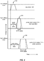
- Timing diagram 302 illustrates raw clock 122 at a low voltage level.
- output pulse clock 114 generated for a read operation is at a high voltage level and comprises a rising edge delay 304d; and as shown in timing diagram 306, output pulse clock 114 generated for a write operation is at a high voltage level and comprises a rising edge delay 306d.
- expected read array delay is accounted for (e.g. through read delay mimic logic 108 of Fig.
- rising edge delay 304d may be made as fast as required to meet the needs of a fast read operation. In comparison, rising edge delay 306d may not need to be fast and thus may be slowed down as required. Further, compared to timing diagram 304, timing diagram 306 illustrates pulse width 306w for a write operation to be wider than pulse width 304w for a read operation, in order to satisfy wider pulse width requirements of write operations as described above.
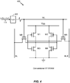
- output pulse clock 114 is used by logic components well known in the art, such as a word line decoder, generally designated by logic 402 in FIG. 4 .
- the operation of 6T SRAM cell 400 is well known.
- Transistors M1, M2, M3, and M4 form a crosscoupled inverter storage element, while access transistors M5 and M6 control read/write operations for the storage element.
- Word line WL controls the gates of access transistors M5 and M6, while complementary bit lines BL and BLB are used to select the particular 6T SRAM cell 400 for write operations and to read out the stored value for read operations.
- output pulse clock 114 may be applied to word line WL in order to meet specific pulse clock requirements for read and write operations, as shown, for example, in FIG. 3 .
- delays introduced by selective delay logic 102 may delay the rising edge of output pulse clock 114 during write operations, which again allows additional set up time for bit lines BL and BLB, and moreover may reduce power because accompanying buffers and drivers may be downsized. Further, the wider pulse width created by selective pulse width widening logic 110 may facilitate write operations even at lower voltage levels, which may lead to improved yield.
- pulse clock generation logic 112 may lead to lower latency and improved reuse of functional blocks, as compared to conventional implementations which have level shifters separated from pulse clock generation logic.
- the feedback path to built-in level shifter via pull-down transistors n3 and n4 may speed up the rising edge of output pulse clock 114 especially when the voltage difference between the low voltage level of raw clock 122 and the high voltage level of output pulse clock 114 is large.
- the latch mechanism in pulse clock generation logic 112 may additionally facilitate holding the logic state of output pulse clock 114 stable.
- an embodiment can include a method for generating a pulse clock (e.g. output pulse clock 114 of FIG. 1 ) comprising: configuring a programmable rising edge delay (e.g. rising edge delay 304d and 306d as illustrated in timing diagrams 304 and 306 of FIG. 3 ) of the pulse clock - Block 502; configuring a programmable pulse width (e.g. width 304w and 306w as illustrated in timing diagrams 304 and 306 of FIG. 3 ) of the pulse clock - Block 504; configuring a level shifter (e.g.
- a software module may reside in RAM memory, flash memory, ROM memory, EPROM memory, EEPROM memory, registers, hard disk, a removable disk, a CD-ROM, or any other form of storage medium known in the art.
- An exemplary storage medium is coupled to the processor such that the processor can read information from, and write information to, the storage medium. In the alternative, the storage medium may be integral to the processor.
- FIG. 6 a block diagram of a particular illustrative embodiment of a wireless device that includes a multi-core processor configured according to exemplary embodiments is depicted and generally designated 600.
- the device 600 includes a digital signal processor (DSP) 664, which may include self-timed pulse clock generation circuit 100 of FIG. 1 .
- DSP 664 may be coupled to memory 632 as shown, wherein the generated pulse clock from self-timed pulse clock generation circuit 100 may be used for memory accesses on memory 632.
- FIG. 6 also shows an external device such as display controller 626 that is coupled to DSP 664 and to display 628.
- An external device such as coder/decoder (CODEC) 634 (e.g., an audio and/or voice CODEC) can also be coupled to DSP 664.
- CODEC coder/decoder
- Other components/external devices, such as wireless controller 640 (which may include a modem) are also illustrated.
- Speaker 636 and microphone 638 can be coupled to CODEC 634.
- FIG. 6 also indicates that wireless controller 640 can be coupled to wireless antenna 642.
- DSP 664, display controller 626, memory 632, CODEC 634, and wireless controller 640 are included in a system-in-package or system-on-chip device 622.
- input device 630 and power supply 644 are coupled to the system-on-chip device 622.
- display 628, input device 630, speaker 636, microphone 638, wireless antenna 642, and power supply 644 are external to the system-on-chip device 622.
- each of display 628, input device 630, speaker 636, microphone 638, wireless antenna 642, and power supply 644 can be coupled to a component of the system-on-chip device 622, such as an interface or a controller.
- FIG. 6 depicts a wireless communications device
- DSP 664 and memory 632 may also be integrated into a set-top box, a music player, a video player, an entertainment unit, a navigation device, a personal digital assistant (PDA), a fixed location data unit, or a computer.
- a processor e.g., DSP 664 may also be integrated into such a device.
- an embodiment of the invention can include a computer readable media embodying a method for generating a pulse clock with a built-in level shifter and a programmable rising edge and programmable pulse width. Accordingly, the invention is not limited to illustrated examples and any means for performing the functionality described herein are included in embodiments of the invention.
Description
- Disclosed embodiments generally relate to pulse clock generation. More particularly, exemplary embodiments are directed to generating pulse clocks with programmable edges and pulse widths configured for varying requirements of different memory access operations.
- Growing demands for extended battery life and high processing speeds in the handheld device and mobile phone industries have created a corresponding need for low power and high performance memory systems. In order to conserve power, on-chip memory is restricted to low supply voltage levels.
- However, conventional memory cells such as 6 Transistor Static Random Access Memory (6T-SRAM) are not capable of operating at very low voltages. A common solution involves the use of multiple voltage domains, such that memory cells may be operated at a relatively high voltage level while other on-chip logic may be operated at lower voltages. In order to achieve multiple voltage domains, level shifters are commonly used to convert low voltage to high voltage and vice versa as needed. However, level shifters introduce latency, which may be undesirable in timing critical paths.
- Document
US6850460 discloses a SRAM array local clock generator having variable delay settings that are programmable via level scan bits. Program bits from the level scan operation are decoded and used to adjust the number of delay elements in the local clock generator path. - In the case of memory systems comprising large arrays of memory cells, locally generated self-timed pulse clocks are often utilized to overcome the effects of device variations (e.g. due to process variations). These pulse clocks may be subjected to conflicting needs for different memory access operations. For example, during a memory read operation it may be desirable for the rising edge of the pulse clock to arrive as fast as possible at memory cells of the memory array being accessed, in order to enable quick read access. Moreover, during the memory read operation it may be desirable for the pulse width of the pulse clock to be narrow, in order to reduce power consumption by disallowing full voltage swings on bit lines.
- On the other hand, memory write operations are usually not timing critical, and thus can tolerate higher arrival delays in the rising edge of the pulse clock. In fact, memory write operations may benefit from delays in the pulse clock so as to allow sufficient set-up time for the data written. In further contrast to read operations, during write operations it may be desirable for the pulse width of the pulse clock to be wider to allow for sufficient write time in order to guarantee successful completion of the write operations, especially at lower supply voltage levels. Conventional pulse clock implementations are not well suited to meet these conflicting needs for read and write operations on memory cells.
- Accordingly, there is a need in the art for solutions which avoid the aforementioned problems associated with level shifters and pulse clocks.
- Exemplary embodiments of the invention are directed to circuits and methods for generating pulse clocks with programmable edges and pulse widths configured for varying requirements of different memory access operations.
- For example, an exemplary embodiment is directed to a method for generating a pulse clock comprising: configuring a programmable rising edge delay of the pulse clock; configuring a programmable pulse width of the pulse clock; configuring a level shifter for shifting a voltage level of the pulse clock; and generating the pulse clock in accordance with the programmed rising edge delay, programmed pulse width, and shifted voltage level.
- Another exemplary embodiment is directed to a pulse clock generation circuit comprising: a selective delay logic to provide a programmable rising edge delay of the pulse clock; a selective pulse width widening logic to provide a programmable pulse width of the pulse clock; a built-in level shifter configured to shift a voltage level of the pulse clock; and logic configured to generate the pulse clock in accordance with the programmed rising edge delay, programmed pulse width, and shifted voltage level.
- Yet another exemplary embodiment is directed to non-transitory computer-readable storage medium comprising code, which, when executed by a processor, causes the processor to perform operations for programming a pulse clock generator, the non-transitory computer-readable storage medium comprising: code for configuring a programmable rising edge delay of the pulse clock; code for configuring a programmable pulse width of the pulse clock; code for configuring a level shifter for shifting a voltage level of the pulse clock; and code for generating the pulse clock in accordance with the programmed rising edge delay, programmed pulse width, and shifted voltage level.
- The accompanying drawings are presented to aid in the description of embodiments of the invention and are provided solely for illustration of the embodiments and not limitation thereof.
-
FIG. 1 illustrates a schematic representation of self-timed pulseclock generation circuit 100 configured according to exemplary embodiments. -
FIG. 2 illustrates a transistor-level schematic view of pulseclock generation logic 112 of the self-timed pulseclock generation circuit 100 ofFIG. 1 . -
FIG. 3 illustrates a timing diagram comprising representations of pulse clocks pertaining to self-timed pulseclock generation circuit 100. -
FIG. 4 illustrates a conventional6T SRAM cell 400 to which a pulse clock generated according to exemplary embodiments may be applied. -
FIG. 5 is a flow chart representing an exemplary method of generating a pulse clock according to exemplary embodiments. -
FIG. 6 illustrates an exemplarywireless communication system 600 in which an embodiment of the disclosure may be advantageously employed. - Aspects of the invention are disclosed in the following description and related drawings directed to specific embodiments of the invention. Alternate embodiments may be devised without departing from the scope of the invention. Additionally, well-known elements of the invention will not be described in detail or will be omitted so as not to obscure the relevant details of the invention.
- The word "exemplary" is used herein to mean "serving as an example, instance, or illustration." Any embodiment described herein as "exemplary" is not necessarily to be construed as preferred or advantageous over other embodiments. Likewise, the term "embodiments of the invention" does not require that all embodiments of the invention include the discussed feature, advantage or mode of operation.
- The terminology used herein is for the purpose of describing particular embodiments only and is not intended to be limiting of embodiments of the invention. As used herein, the singular forms "a", "an" and "the" are intended to include the plural forms as well, unless the context clearly indicates otherwise. It will be further understood that the terms "comprises", "comprising,", "includes" and/or "including", when used herein, specify the presence of stated features, integers, steps, operations, elements, and/or components, but do not preclude the presence or addition of one or more other features, integers, steps, operations, elements, components, and/or groups thereof.
- Further, many embodiments are described in terms of sequences of actions to be performed by, for example, elements of a computing device. It will be recognized that various actions described herein can be performed by specific circuits (e.g., application specific integrated circuits (ASICs)), by program instructions being executed by one or more processors, or by a combination of both. Additionally, these sequence of actions described herein can be considered to be embodied entirely within any form of computer readable storage medium having stored therein a corresponding set of computer instructions that upon execution would cause an associated processor to perform the functionality described herein. Thus, the various aspects of the invention may be embodied in a number of different forms, all of which have been contemplated to be within the scope of the claimed subject matter. In addition, for each of the embodiments described herein, the corresponding form of any such embodiments may be described herein as, for example, "logic configured to" perform the described action.
- Exemplary embodiments are directed to self-timed pulse clock generation circuits configured for programmable pulse width and rising edge delays in order to meet conflicting requirements of read and write operations. Further, exemplary embodiments may include a built-in level shifter configured to convert a raw clock in a low voltage domain to pulse clocks for read and write operations in high voltage domain without introducing additional delays from a separate voltage level shifter, while also preventing glitches and charge sharing problems which may occur in conventional implementations.
- With reference now to
FIG. 1 , self-timed pulseclock generation circuit 100 configured according to exemplary embodiments is illustrated.Raw clock 122 may be input to self-timed pulseclock generation circuit 100, and may serve as a base clock for generating customized clock pulses for read and write operations.Raw clock 122 may be generated by known techniques such as by the use of piezoelectric crystals, etc.Raw clock 122 may be made available at a low voltage level or may be derived from a low voltage domain. -
Raw clock 122 may first enterselective delay logic 102, whereinraw clock 122 may be delayed selectively for write operations.Programmable delay logic 104, read/writecontrol 126 andselector 106 may be configured as shown for selectively delayingraw clock 122. In one example, if a read operation is indicated by read/writecontrol 126, thenraw clock 122 may be selected byselector 106 to form the selectively delayedoutput clock clk_d1 116. On the other hand, if read/writecontrol 126 indicates a write operation, thenprogrammable delay logic 104 may delayraw clock 122 by a desired amount and generate adelayed clock 124, which may then be selected byselector 106 to form the selectively delayedoutput clock clk_d1 116.Programmable delay logic 104 may be implemented by known techniques, such as, by controlling a number of inverters or buffer elements to be coupled in series. Effective sizes of these inverters or buffer elements may also be controlled to adjust the delay amount. Skilled persons will recognize suitable implementations forprogrammable delay logic 104. - The selectively delayed output clock,
clk_d1 116, thus generated, may then enter pulseclock generation logic 112. Pulseclock generation logic 112 may ultimately outputpulse clock 114 which meets above-noted requirements for read and write operations in exemplary embodiments. Pulseclock generation logic 112 may include logic for voltage level shifting, such thatoutput pulse clock 114 is made available at a high voltage level without introducing unwanted latency from a separate voltage level shifter. Further, pulseclock generation logic 112 may be configured to eliminate glitches inoutput pulse clock 114.Feedback path 118 fromoutput pulse clock 114 back to pulseclock generation logic 112 throughreset 121 may include read delaymimic logic 108 and selective pulsewidth widening logic 110 as shown.Feedback path 118 may provide a self-resetting and thus self-timing functionality to pulseclock generation logic 112. Pulseclock generation logic 112, read delaymimic logic 108, and selective pulsewidth widening logic 110 will now be described in further detail. - With reference now to
FIG. 2 , an expanded view of pulseclock generation logic 112 is provided, which includes a transistor-level schematic.Enable 130 and power-up reset 128 are input toclock generation logic 112 from an external source (not shown) to enable or reset theoutput pulse clock 114. An exemplary operation of pulseclock generation logic 112 will now be described. Initially, power-up reset 128 is driven high, thus causing the output of inverter i6 to be driven low and triggering pull-up transistor p3 to pull uplat_node 142 and thereby drivingoutput pulse clock 114 low via inverter i5. It will be observed that pull-up transistor p3 is in the high voltage domain, as indicated inFIG. 2 . Thus,output pulse clock 114 is derived in the high voltage domain. - Thereafter, power-
up reset 128 is driven low and enable 130 is driven high. The selectively delayed output clock,clk_d1 116 traverses through inverters i1, i2, and i3, and thus the output of i3 presents an inverted and delayed pulse following clk_d1. At the point when the output of i3 also rises, both inputs to nand1, i.e. the output of i3 and enable 130 are high, thus causing the output of nand1 to be low. This in turn means both inputs of nor1, i.e. the output of nand1 and the power-up reset 128 are low, and thus,node clk_d2 140 is driven high, thereby turning on pull-down transistor n2. Further, pull-down transistor n4 will now be turned on because the output of inverter i6 will be driven high. - A first instance of a rising edge of
raw clock 122 will now be considered. It will be recalled that the selectively delayedoutput clock clk_d1 116 is a selectively delayed version ofraw clock 122. Bothraw clock 122 and selectively delayedoutput clock clk_d1 116 may be in the low voltage domain. Thus, a rising edge ofraw clock 122 may cause a rising edge of selectively delayedoutput clock clk_d1 116 after a delay, and then turn on pull-down transistor n1. At this instance in time pull-down transistor n3 will remain turned off. It will be noticed fromFIG. 2 that selectively delayedoutput clock clk_d1 116 is coupled to the gate of pull-up transistor p5 andnode clk_d2 140 is coupled to the gate of transistor p6. Accordingly, pull-up transistors p5 and p6 will be partially turned off, because the source voltages of pull-up transistors p5 and p6 are in the high voltage domain and their gate voltages are in the low voltage domain; and all four pull-down transistors n0, n1, n2, and n4 will be turned on at this instance. Therefore, both nodes int_node 144 andlat_node 142 will be pulled down and inverter i5 will driveoutput pulse clock 114 high. During the time that lat_node 142 is being pulled down, pull-down transistor n3 will be turned on, which will provide additional current source to speed up the pull down process oflat_node 142 andint_node 144 . It will be recalled thatoutput pulse clock 114 is already in the high voltage domain. Accordingly, the rising edge ofraw clock 122 in the low voltage domain creates a rising edge ofoutput pulse clock 114 in the high voltage domain without requiring additional voltage level shifting logic. While pull-up transistors p5 and p6 being turned off halfway may incur minor delay and power consumption costs, these costs may be offset by the additional pull-down path provided by pull-down transistors n3 and n4. - Now, lat_node 142 will remain in the low state and
pulse clock 114 will remain in the high state due to the latch created by inverter i4 and the combination of pull-up transistors p4, p6 and pull-down transistors n3, n4, until a reset mechanism returns lat_node 142 to high state, thus drivingoutput pulse clock 114 low. Reset 121, which will be described in further detail below, can control the falling edge ofoutput pulse clock 114. It will be recognized that controlling the time period between the rising edge ofoutput pulse clock 114 and the falling edge ofoutput pulse clock 114 will determine the width of the clock pulse derived atoutput pulse clock 114. - Returning now to
FIG. 1 , selective pulsewidth widening logic 110 may be employed to selectively expand the pulse width between rising and falling edges ofoutput pulse clock 114. Similar toselective delay logic 102, selective pulsewidth widening logic 110 may employmultiplexor 107 to choose between the input signal without added delays and a delayed version of the input signal, based on read/write control 126. The timing of read/write control 126 may be appropriately adjusted bybuffer 127 to account for delays in reaching selective pulsewidth widening block 110 after passing throughselective delay block 102 which was previously discussed. Accordingly, depending on whether the operation is a read or a write, the delay path through selective pulse width widening logic may be controlled, such that the pulse width for write operations is made wider. In other words,output 120 of read delay mimic logic 108 (which will be discussed in further detail below) may be selectively delayed to cause the width of the output of selective pulsewidth widening logic 110, reset 121 to change. This will control the time it takes forreset 121 to rise from a low to high level and then fall back to the low level. - Once reset 121 falls, a next rising edge of
output pulse clock 114 may be generated by repeating the above process. The next falling edge may be suitably delayed for read operations by read delaymimic logic 108. In other words, read delaymimic logic 108 is configured to ultimately delay the falling edge ofoutput pulse clock 114, thus controlling the pulse width. As will be recalled, the rising edge ofoutput pulse clock 114 is controlled byselective delay logic 102. - With combined reference now to
FIGS. 1 and2 ,feedback path 118 fromoutput pulse clock 114 to reset 121 will now be described. As shown inFIG. 1 , this path comprises read delaymimic logic 108 and selective pulsewidth widening logic 110. - Read delay
mimic logic 108 may be included to control the delay in the falling edge ofoutput pulse clock 114 from the rising edge ofoutput pulse clock 114 in order to account for memory array access delays encountered during a read operation. For example, read delaymimic logic 108 may be configured to provide a delay corresponding to the delay which may be incurred in accessing a memory cell in the memory array. Read delay mimic logic may comprise a programmable delay element to match an expected read access delay. Thus, the rising edge ofoutput pulse clock 114 will be delayed by read delaymimic logic 108 to form the rising edge ofoutput 120. In the case of read operations, selective pulsewidth widening logic 110 will select the input without any delay added and the rising edge ofoutput 120 will essentially appear as the rising edge ofreset 121, which is inverted by inverter i7 in pulseclock generation logic 112. With particular reference now toFIG. 2 , the inverter formed by pull-up transistor p0 and pull-down transistor n0 will reset lat_node 142 to a high state. In other words, the feedback loop including readmimic delay logic 108 ofFIG. 1 will essentially ensure that the falling edge ofoutput pulse clock 114 is made available at a delayed time in the high voltage domain in the case of read operations. - Turning again to the first instance of the rising edge of
raw clock 122 after coming out of reset,node clk_d2 140 will fall after the rising edge of selectively delayedoutput clock clk_d1 116 traverses inverters i1, i2, i3, and nand1 and nor1. This will cause pull-down transistor n2 to be turned off, and also pull-up transistor p6 to be turned on. This will cause lat_node 142 to rise, thus creating the falling edge ofoutput pulse clock 114. At this point in time, pull-down transistor n1 may either be turned on or off, without affecting the latching function oflat_node 142. When the falling edge of selectively delayed output clock clk_d1 116 (after being selectively delayed from the falling edge of raw clock 122) comes through, pull-down transistor n1 will also be turned off, and pull-up transistor p5 will be turned on. Turning off both pull-down transistors n1 and n2 will provide additional leakage power saving through the path comprising pull-down transistors n1 and n2. In the case of write operations, selective pulsewidth widening logic 110 will selectively introduce an additional delay in the feedback path beforereset 121 may be asserted and thus allowing lat_node 142 to rise and create the falling edge ofoutput pulse clock 114. In this manner, write operations will have a wider pulse width. As previously described, a wider pulse width may facilitate write operations by providing additional time for completion of write operations (which as will be recalled, are usually not timing critical). - It will be recognized that turning on both pull-down transistors n1 and n2 is a self-timed process. The time period for which pull-down transistors n1 and n2 are turned on may be determined by the delay through inverters i1, i2, i3, and gates nand1 and nor1. In general, pull-down transistors n1 and n2 will be turned off before
reset 121 is de-asserted. Accordingly, in cases where read/write operations require multiple cycles for their completion, a single pulse ofenable 130 may be provided during the entire operation, thus ensuring that only a single pulse ofoutput pulse clock 114 is generated for the duration of the entire operation. - Accordingly, it is seen that the rising edge of
output pulse clock 114 may be delayed fromraw clock 122 by a controllable amount for read operations and write operations. The latch mechanism including inverter i4 and the combination of pull-up transistors p4, p6 and pull-down transistors n3, n4 will holdoutput pulse clock 114 at a high state until a falling edge is imposed after a controllable time period for read and write operations by assertingsignal reset 121. - Now it will be noted that pulse
clock generation logic 112 is also configured to avoid glitches and undesirable charge sharing which may occur, for example, betweenlat_node 142 andint_node 144. When reset 121 changes between high and low state, it will be recognized thatlat_node 142 may remain at a high state due to the latch mechanism, but int_node 144 may fall to a low state, thus causing a large voltage differential to occur between drain and source nodes of pull-down transistor n0. This may lead to unwanted charge sharing problems. In order to prevent such problems from arising,int_node 144 may be pulled up to high state using the pull-up transistors p5, p6, p1 and p2. Thus, bothlat_node 142 andint_node 144 will be in the high state, and a large differential voltage will no longer affect pull-down transistor n0. - With reference now to
FIG. 3 , a timing diagram comprising exemplary schematic representations ofraw clock 122 andouptut pulse clock 114 for read and write operations as described above, is illustrated. The horizontal axis comprises time and the vertical axis comprises voltage levels as shown. Timing diagram 302 illustratesraw clock 122 at a low voltage level. As shown in timing diagram 304,output pulse clock 114 generated for a read operation is at a high voltage level and comprises a risingedge delay 304d; and as shown in timing diagram 306,output pulse clock 114 generated for a write operation is at a high voltage level and comprises a risingedge delay 306d. After expected read array delay is accounted for (e.g. through read delaymimic logic 108 ofFig. 1 ) risingedge delay 304d may be made as fast as required to meet the needs of a fast read operation. In comparison, risingedge delay 306d may not need to be fast and thus may be slowed down as required. Further, compared to timing diagram 304, timing diagram 306 illustratespulse width 306w for a write operation to be wider thanpulse width 304w for a read operation, in order to satisfy wider pulse width requirements of write operations as described above. - With reference now to
FIG. 4 , conventional6T SRAM cell 400 is illustrated to whichoutput pulse clock 114 generated according to exemplary embodiments may be applied. As shown,output pulse clock 114 is used by logic components well known in the art, such as a word line decoder, generally designated bylogic 402 inFIG. 4 . The operation of6T SRAM cell 400 is well known. Transistors M1, M2, M3, and M4 form a crosscoupled inverter storage element, while access transistors M5 and M6 control read/write operations for the storage element. Word line WL controls the gates of access transistors M5 and M6, while complementary bit lines BL and BLB are used to select the particular6T SRAM cell 400 for write operations and to read out the stored value for read operations. As shown,output pulse clock 114 may be applied to word line WL in order to meet specific pulse clock requirements for read and write operations, as shown, for example, inFIG. 3 . - It will be seen that with regard to write operations in exemplary embodiments, delays introduced by
selective delay logic 102 may delay the rising edge ofoutput pulse clock 114 during write operations, which again allows additional set up time for bit lines BL and BLB, and moreover may reduce power because accompanying buffers and drivers may be downsized. Further, the wider pulse width created by selective pulsewidth widening logic 110 may facilitate write operations even at lower voltage levels, which may lead to improved yield. - Additionally, integrating the voltage level shifting mechanism in pulse
clock generation logic 112 may lead to lower latency and improved reuse of functional blocks, as compared to conventional implementations which have level shifters separated from pulse clock generation logic. The feedback path to built-in level shifter via pull-down transistors n3 and n4 may speed up the rising edge ofoutput pulse clock 114 especially when the voltage difference between the low voltage level ofraw clock 122 and the high voltage level ofoutput pulse clock 114 is large. The latch mechanism in pulseclock generation logic 112 may additionally facilitate holding the logic state ofoutput pulse clock 114 stable. - It will be appreciated that embodiments include various methods for performing the processes, functions and/or algorithms disclosed herein. For example, as illustrated in
FIG. 5 , an embodiment can include a method for generating a pulse clock (e.g.output pulse clock 114 ofFIG. 1 ) comprising: configuring a programmable rising edge delay (e.g. risingedge delay FIG. 3 ) of the pulse clock -Block 502; configuring a programmable pulse width (e.g. width FIG. 3 ) of the pulse clock -Block 504; configuring a level shifter (e.g. built-in level shifter in pulseclock generation logic 112 ofFIGS. 1-2 ) for shifting a voltage level of the pulse clock -Block 506; and generating the pulse clock in accordance with the programmed rising edge delay, pulse width, and shifted voltage level -Block 508. - Those of skill in the art will appreciate that information and signals may be represented using any of a variety of different technologies and techniques. For example, data, instructions, commands, information, signals, bits, symbols, and chips that may be referenced throughout the above description may be represented by voltages, currents, electromagnetic waves, magnetic fields or particles, optical fields or particles, or any combination thereof.
- Further, those of skill in the art will appreciate that the various illustrative logical blocks, modules, circuits, and algorithm steps described in connection with the embodiments disclosed herein may be implemented as electronic hardware, computer software, or combinations of both. To clearly illustrate this interchangeability of hardware and software, various illustrative components, blocks, modules, circuits, and steps have been described above generally in terms of their functionality. Whether such functionality is implemented as hardware or software depends upon the particular application and design constraints imposed on the overall system. Skilled artisans may implement the described functionality in varying ways for each particular application, but such implementation decisions should not be interpreted as causing a departure from the scope of the present invention.
- The methods, sequences and/or algorithms described in connection with the embodiments disclosed herein may be embodied directly in hardware, in a software module executed by a processor, or in a combination of the two. A software module may reside in RAM memory, flash memory, ROM memory, EPROM memory, EEPROM memory, registers, hard disk, a removable disk, a CD-ROM, or any other form of storage medium known in the art. An exemplary storage medium is coupled to the processor such that the processor can read information from, and write information to, the storage medium. In the alternative, the storage medium may be integral to the processor.
- Referring to
FIG. 6 , a block diagram of a particular illustrative embodiment of a wireless device that includes a multi-core processor configured according to exemplary embodiments is depicted and generally designated 600. Thedevice 600 includes a digital signal processor (DSP) 664, which may include self-timed pulseclock generation circuit 100 ofFIG. 1 .DSP 664 may be coupled tomemory 632 as shown, wherein the generated pulse clock from self-timed pulseclock generation circuit 100 may be used for memory accesses onmemory 632. For example,FIG. 6 also shows an external device such asdisplay controller 626 that is coupled toDSP 664 and to display 628. An external device such as coder/decoder (CODEC) 634 (e.g., an audio and/or voice CODEC) can also be coupled toDSP 664. Other components/external devices, such as wireless controller 640 (which may include a modem) are also illustrated.Speaker 636 andmicrophone 638 can be coupled toCODEC 634.FIG. 6 also indicates thatwireless controller 640 can be coupled towireless antenna 642. In a particular embodiment,DSP 664,display controller 626,memory 632,CODEC 634, andwireless controller 640 are included in a system-in-package or system-on-chip device 622. - In a particular embodiment,
input device 630 andpower supply 644 are coupled to the system-on-chip device 622. Moreover, in a particular embodiment, as illustrated inFIG. 6 ,display 628,input device 630,speaker 636,microphone 638,wireless antenna 642, andpower supply 644 are external to the system-on-chip device 622. However, each ofdisplay 628,input device 630,speaker 636,microphone 638,wireless antenna 642, andpower supply 644 can be coupled to a component of the system-on-chip device 622, such as an interface or a controller. - It should be noted that although
FIG. 6 depicts a wireless communications device,DSP 664 andmemory 632 may also be integrated into a set-top box, a music player, a video player, an entertainment unit, a navigation device, a personal digital assistant (PDA), a fixed location data unit, or a computer. A processor (e.g., DSP 664) may also be integrated into such a device. - Accordingly, an embodiment of the invention can include a computer readable media embodying a method for generating a pulse clock with a built-in level shifter and a programmable rising edge and programmable pulse width. Accordingly, the invention is not limited to illustrated examples and any means for performing the functionality described herein are included in embodiments of the invention.
- While the foregoing disclosure shows illustrative embodiments of the invention, it should be noted that various changes and modifications could be made herein without departing from the scope of the invention as defined by the appended claims. The functions, steps and/or actions of the method claims in accordance with the embodiments of the invention described herein need not be performed in any particular order. Furthermore, although elements of the invention may be described or claimed in the singular, the plural is contemplated unless limitation to the singular is explicitly stated.
Claims (14)
- A method for generating a pulse clock comprising:configuring a pulse clock generation circuit (100) to output the pulse clock in a high voltage domain based on a raw clock input (122) at a low voltage domain, the pulse clock generation circuit comprising a built-in level shifter configured to provide voltage level shifting from the low voltage domain to the high voltage domain,wherein a rising edge of the pulse clock is delayed from a rising edge of the raw clock by a programmable rising edge delay provided by a selective delay logic (102), andwherein a programmable pulse width of the pulse clock is based on a feedback path (118) from the output of the pulse clock generation circuit in the high voltage domain to the input of the pulse clock generation circuit in the low voltage domain,the feedback path comprising a selective pulse width widening logic (110) to provide the programmable pulse width and a read delay mimic logic (108) to provide a read delay to match an expected memory array read access delay corresponding to the delay which is incurred in accessing a memory cell in the memory array.
- The method of claim 1, comprising configuring a single pulse of the pulse clock to span an entire duration of a multiple cycle memory read or write operation.
- The method of claim 1, further comprising self-resetting the pulse clock generator through the feedback path.
- The method of claim 1, wherein the programmable rising edge delay for a memory write operation is greater than the read delay.
- The method of claim 1, further comprising providing self-resetting and self-timing functionality to the pulse clock generation logic through the feedback path.
- The method of claim 1, wherein the programmable pulse width for a memory write operation is programmed to be greater than the programmable pulse width for a memory read operation.
- A pulse clock generation circuit (100) comprising:an input at a low voltage domain coupled to a raw clock (122);an output at a high voltage domain connected to a pulse clock (114); a pulse clock generation logic (112) configured to output the pulse clock (114); a built-in level shifter configured to provide voltage level shifting from the low voltage domain to the high voltage domain;a selective delay logic (102) to delay a rising edge of the pulse clock from a rising edge of the raw clock by a programmable rising edge delay; anda feedback path (118) from the output of the pulse clock generation logic (112) in the high voltage domain to the input of the pulse clock generation logic (112) in the low voltage domain, the feedback path comprising a selective pulse width widening logic (110) to provide a programmable pulse width of the pulse clock and a read delay mimic logic (108) to provide a read delay to match a memory array read access delay corresponding to the delay which is incurred in accessing a memory cell in the memory array.
- The pulse clock generation circuit (100) of claim 7, wherein the feedback path is further configured to provide self-resetting and self-timing functionality to the pulse clock generation circuit (100)
- The pulse clock generation circuit (100) of claim 7, further comprising an input reset signal, connected to the feedback path, configured to drive the pulse clock to low logic level.
- The pulse clock generation circuit (100) of claim 7, further comprising a latch to stabilize the pulse clock.
- The pulse clock generation circuit (100) of claim 10, further comprising pull-up transistors (p3) to reduce charge sharing created by the latch.
- The pulse clock generation circuit (100) of claim 7, further comprising an input enable signal (130) to enable pulsing behavior of the pulse clock.
- The pulse clock generation circuit (100) of claim 12, wherein the input enable signal (130) is configured to enable pulsing behavior of the pulse clock for a plurality of clock cycles corresponding to the time period for completion of a memory access operation.
- A computer program product comprising a computer readable medium, the computer readable medium comprising at least one instruction for causing a computer or processor to perform a method in accordance with claims 1-6.
Applications Claiming Priority (2)
| Application Number | Priority Date | Filing Date | Title |
|---|---|---|---|
| US13/433,891 US8638153B2 (en) | 2012-03-29 | 2012-03-29 | Pulse clock generation logic with built-in level shifter and programmable rising edge and pulse width |
| PCT/US2013/034414 WO2013149040A1 (en) | 2012-03-29 | 2013-03-28 | A pulse clock generation logic with built-in level shifter and programmable rising edge and pulse width |
Publications (2)
| Publication Number | Publication Date |
|---|---|
| EP2831694A1 EP2831694A1 (en) | 2015-02-04 |
| EP2831694B1 true EP2831694B1 (en) | 2017-08-23 |
Family
ID=48083683
Family Applications (1)
| Application Number | Title | Priority Date | Filing Date |
|---|---|---|---|
| EP13715579.2A Not-in-force EP2831694B1 (en) | 2012-03-29 | 2013-03-28 | A pulse clock generation logic with built-in level shifter and programmable rising edge and pulse width |
Country Status (6)
| Country | Link |
|---|---|
| US (1) | US8638153B2 (en) |
| EP (1) | EP2831694B1 (en) |
| JP (1) | JP6242852B2 (en) |
| KR (1) | KR20140139595A (en) |
| CN (1) | CN104204992B (en) |
| WO (1) | WO2013149040A1 (en) |
Families Citing this family (13)
| Publication number | Priority date | Publication date | Assignee | Title |
|---|---|---|---|---|
| KR20160127168A (en) * | 2013-03-15 | 2016-11-02 | 인텔 코포레이션 | A memory system |
| CN104680991B (en) * | 2015-03-03 | 2017-03-08 | 深圳市华星光电技术有限公司 | Level shift circuit and level shift method for GOA framework liquid crystal panel |
| KR102295058B1 (en) | 2015-08-19 | 2021-08-31 | 삼성전자주식회사 | Semiconductor memory system and semiconductor memory device and operating method for semiconductor memory device |
| US9564901B1 (en) | 2015-12-17 | 2017-02-07 | Apple Inc. | Self-timed dynamic level shifter with falling edge generator |
| CN106940423B (en) * | 2016-01-05 | 2023-02-24 | 华润微集成电路(无锡)有限公司 | Built-in test circuit of multi-functional chip |
| US9607674B1 (en) * | 2016-01-06 | 2017-03-28 | Qualcomm Incorporated | Pulse latch reset tracking at high differential voltage |
| US10163508B2 (en) | 2016-02-26 | 2018-12-25 | Intel Corporation | Supporting multiple memory types in a memory slot |
| US10615796B2 (en) * | 2016-07-29 | 2020-04-07 | Qualcomm Incorporated | Level shifter |
| US10163474B2 (en) * | 2016-09-22 | 2018-12-25 | Qualcomm Incorporated | Apparatus and method of clock shaping for memory |
| US9990984B1 (en) | 2016-12-06 | 2018-06-05 | Qualcomm Incorporated | Pulse-stretcher clock generator circuit for high speed memory subsystems |
| CN106941347B (en) * | 2017-03-17 | 2019-08-06 | 中国电子科技集团公司第二十四研究所 | Duty cycle adjustment device and method |
| US10389335B1 (en) | 2018-05-04 | 2019-08-20 | Apple Inc. | Clock pulse generation circuit |
| CN114006605B (en) * | 2021-12-31 | 2022-05-10 | 峰岹科技(深圳)股份有限公司 | Single-edge delay circuit |
Family Cites Families (13)
| Publication number | Priority date | Publication date | Assignee | Title |
|---|---|---|---|---|
| US5027323A (en) | 1988-01-14 | 1991-06-25 | Hitachi, Ltd. | Write pulse signal generating circuit for a semiconductor memory device |
| US6072348A (en) * | 1997-07-09 | 2000-06-06 | Xilinx, Inc. | Programmable power reduction in a clock-distribution circuit |
| US5929684A (en) * | 1998-03-06 | 1999-07-27 | Siemens Aktiengesellschaft | Feedback pulse generators |
| JP2003030991A (en) * | 2001-07-12 | 2003-01-31 | Sanyo Electric Co Ltd | Memory |
| CN2544466Y (en) * | 2002-01-25 | 2003-04-09 | 威盛电子股份有限公司 | No sudden wave interfefence clock pulse output circuit |
| US6975154B1 (en) * | 2003-04-29 | 2005-12-13 | Altera Corporation | Reduced power consumption clock network |
| WO2005018091A1 (en) * | 2003-08-13 | 2005-02-24 | Fujitsu Limited | Pulse generation circuit |
| US6850460B1 (en) | 2004-05-12 | 2005-02-01 | International Business Machines Corporation | High performance programmable array local clock generator |
| US7180353B2 (en) | 2005-02-03 | 2007-02-20 | Mediatek Incorporation | Apparatus and method for low power clock distribution |
| US7609583B2 (en) | 2007-11-12 | 2009-10-27 | Micron Technology, Inc. | Selective edge phase mixing |
| US7876631B2 (en) * | 2008-12-17 | 2011-01-25 | Qualcomm Incorporated | Self-tuning of signal path delay in circuit employing multiple voltage domains |
| US8102720B2 (en) | 2009-02-02 | 2012-01-24 | Qualcomm Incorporated | System and method of pulse generation |
| CN101847991B (en) * | 2009-03-27 | 2012-01-11 | 台湾积体电路制造股份有限公司 | Clock generators, memory circuits, and methods for generating an internal clock signal |
-
2012
- 2012-03-29 US US13/433,891 patent/US8638153B2/en not_active Expired - Fee Related
-
2013
- 2013-03-28 EP EP13715579.2A patent/EP2831694B1/en not_active Not-in-force
- 2013-03-28 JP JP2015503586A patent/JP6242852B2/en not_active Expired - Fee Related
- 2013-03-28 KR KR1020147029964A patent/KR20140139595A/en not_active Application Discontinuation
- 2013-03-28 CN CN201380016930.XA patent/CN104204992B/en not_active Expired - Fee Related
- 2013-03-28 WO PCT/US2013/034414 patent/WO2013149040A1/en active Application Filing
Non-Patent Citations (1)
| Title |
|---|
| None * |
Also Published As
| Publication number | Publication date |
|---|---|
| WO2013149040A1 (en) | 2013-10-03 |
| CN104204992A (en) | 2014-12-10 |
| EP2831694A1 (en) | 2015-02-04 |
| US20130257498A1 (en) | 2013-10-03 |
| KR20140139595A (en) | 2014-12-05 |
| CN104204992B (en) | 2017-05-17 |
| US8638153B2 (en) | 2014-01-28 |
| JP6242852B2 (en) | 2017-12-06 |
| JP2015520434A (en) | 2015-07-16 |
Similar Documents
| Publication | Publication Date | Title |
|---|---|---|
| EP2831694B1 (en) | A pulse clock generation logic with built-in level shifter and programmable rising edge and pulse width | |
| US10461747B2 (en) | Low power clock gating circuit | |
| JP5055448B2 (en) | Semiconductor device that can use the delay lock state information of the delay lock loop | |
| KR101018706B1 (en) | Semiconductor memory device and the method for operating the same | |
| US8994402B2 (en) | Level shifter circuit optimized for metastability resolution and integrated level shifter and metastability resolution circuit | |
| JP5282560B2 (en) | Semiconductor device and system | |
| EP3198609B1 (en) | Voltage level shifted self-clocked write assistance | |
| US9196330B2 (en) | Mimicking multi-voltage domain wordline decoding logic for a memory array | |
| US9036446B2 (en) | Global reset with replica for pulse latch pre-decoders | |
| EP2951943B1 (en) | Rotational synchronizer circuit for metastablity resolution | |
| KR102293806B1 (en) | Static random access memory (sram) global bitline circuits for reducing power glitches during memory read accesses, and related methods and systems | |
| US20180122458A1 (en) | Multi-port memory and semiconductor device | |
| US7714632B2 (en) | Clock control circuit and semiconductor integrated circuit using the same | |
| US10491197B2 (en) | Flop circuit with integrated clock gating circuit | |
| KR20100095830A (en) | Shift register having glitch free function in power saving operation | |
| JP2002304887A (en) | Semiconductor integrated circuit | |
| US9911472B1 (en) | Write bitline driver for a dual voltage domain | |
| US10659015B2 (en) | Method, apparatus, and system for a level shifting latch with embedded logic | |
| US20180152176A1 (en) | Voltage aware circuit for dual voltage domain signals | |
| KR100656469B1 (en) | Apparatus for controlling power down of semiconductor memory | |
| US7990801B2 (en) | Internal write/read pulse generating circuit of a semiconductor memory apparatus | |
| KR100712986B1 (en) | Latch circuit | |
| KR101819134B1 (en) | Semiconductor Memory Apparatus | |
| JP2014078313A (en) | Semiconductor device |
Legal Events
| Date | Code | Title | Description |
|---|---|---|---|
| PUAI | Public reference made under article 153(3) epc to a published international application that has entered the european phase |
Free format text: ORIGINAL CODE: 0009012 |
|
| 17P | Request for examination filed |
Effective date: 20140910 |
|
| AK | Designated contracting states |
Kind code of ref document: A1 Designated state(s): AL AT BE BG CH CY CZ DE DK EE ES FI FR GB GR HR HU IE IS IT LI LT LU LV MC MK MT NL NO PL PT RO RS SE SI SK SM TR |
|
| AX | Request for extension of the european patent |
Extension state: BA ME |
|
| DAX | Request for extension of the european patent (deleted) | ||
| REG | Reference to a national code |
Ref country code: DE Ref legal event code: R079 Ref document number: 602013025418 Country of ref document: DE Free format text: PREVIOUS MAIN CLASS: G06F0001040000 Ipc: G11C0011417000 |
|
| RIC1 | Information provided on ipc code assigned before grant |
Ipc: G11C 11/417 20060101AFI20170228BHEP Ipc: G11C 11/418 20060101ALI20170228BHEP Ipc: G06F 1/04 20060101ALI20170228BHEP Ipc: G11C 11/419 20060101ALI20170228BHEP Ipc: G11C 7/22 20060101ALI20170228BHEP |
|
| GRAP | Despatch of communication of intention to grant a patent |
Free format text: ORIGINAL CODE: EPIDOSNIGR1 |
|
| INTG | Intention to grant announced |
Effective date: 20170410 |
|
| GRAS | Grant fee paid |
Free format text: ORIGINAL CODE: EPIDOSNIGR3 |
|
| GRAA | (expected) grant |
Free format text: ORIGINAL CODE: 0009210 |
|
| AK | Designated contracting states |
Kind code of ref document: B1 Designated state(s): AL AT BE BG CH CY CZ DE DK EE ES FI FR GB GR HR HU IE IS IT LI LT LU LV MC MK MT NL NO PL PT RO RS SE SI SK SM TR |
|
| REG | Reference to a national code |
Ref country code: GB Ref legal event code: FG4D |
|
| REG | Reference to a national code |
Ref country code: CH Ref legal event code: EP |
|
| REG | Reference to a national code |
Ref country code: AT Ref legal event code: REF Ref document number: 922144 Country of ref document: AT Kind code of ref document: T Effective date: 20170915 |
|
| REG | Reference to a national code |
Ref country code: IE Ref legal event code: FG4D |
|
| REG | Reference to a national code |
Ref country code: DE Ref legal event code: R096 Ref document number: 602013025418 Country of ref document: DE |
|
| REG | Reference to a national code |
Ref country code: NL Ref legal event code: MP Effective date: 20170823 |
|
| REG | Reference to a national code |
Ref country code: LT Ref legal event code: MG4D |
|
| REG | Reference to a national code |
Ref country code: AT Ref legal event code: MK05 Ref document number: 922144 Country of ref document: AT Kind code of ref document: T Effective date: 20170823 |
|
| PG25 | Lapsed in a contracting state [announced via postgrant information from national office to epo] |
Ref country code: LT Free format text: LAPSE BECAUSE OF FAILURE TO SUBMIT A TRANSLATION OF THE DESCRIPTION OR TO PAY THE FEE WITHIN THE PRESCRIBED TIME-LIMIT Effective date: 20170823 Ref country code: SE Free format text: LAPSE BECAUSE OF FAILURE TO SUBMIT A TRANSLATION OF THE DESCRIPTION OR TO PAY THE FEE WITHIN THE PRESCRIBED TIME-LIMIT Effective date: 20170823 Ref country code: AT Free format text: LAPSE BECAUSE OF FAILURE TO SUBMIT A TRANSLATION OF THE DESCRIPTION OR TO PAY THE FEE WITHIN THE PRESCRIBED TIME-LIMIT Effective date: 20170823 Ref country code: NL Free format text: LAPSE BECAUSE OF FAILURE TO SUBMIT A TRANSLATION OF THE DESCRIPTION OR TO PAY THE FEE WITHIN THE PRESCRIBED TIME-LIMIT Effective date: 20170823 Ref country code: NO Free format text: LAPSE BECAUSE OF FAILURE TO SUBMIT A TRANSLATION OF THE DESCRIPTION OR TO PAY THE FEE WITHIN THE PRESCRIBED TIME-LIMIT Effective date: 20171123 Ref country code: HR Free format text: LAPSE BECAUSE OF FAILURE TO SUBMIT A TRANSLATION OF THE DESCRIPTION OR TO PAY THE FEE WITHIN THE PRESCRIBED TIME-LIMIT Effective date: 20170823 Ref country code: FI Free format text: LAPSE BECAUSE OF FAILURE TO SUBMIT A TRANSLATION OF THE DESCRIPTION OR TO PAY THE FEE WITHIN THE PRESCRIBED TIME-LIMIT Effective date: 20170823 |
|
| REG | Reference to a national code |
Ref country code: FR Ref legal event code: PLFP Year of fee payment: 6 |
|
| PG25 | Lapsed in a contracting state [announced via postgrant information from national office to epo] |
Ref country code: GR Free format text: LAPSE BECAUSE OF FAILURE TO SUBMIT A TRANSLATION OF THE DESCRIPTION OR TO PAY THE FEE WITHIN THE PRESCRIBED TIME-LIMIT Effective date: 20171124 Ref country code: PL Free format text: LAPSE BECAUSE OF FAILURE TO SUBMIT A TRANSLATION OF THE DESCRIPTION OR TO PAY THE FEE WITHIN THE PRESCRIBED TIME-LIMIT Effective date: 20170823 Ref country code: RS Free format text: LAPSE BECAUSE OF FAILURE TO SUBMIT A TRANSLATION OF THE DESCRIPTION OR TO PAY THE FEE WITHIN THE PRESCRIBED TIME-LIMIT Effective date: 20170823 Ref country code: IS Free format text: LAPSE BECAUSE OF FAILURE TO SUBMIT A TRANSLATION OF THE DESCRIPTION OR TO PAY THE FEE WITHIN THE PRESCRIBED TIME-LIMIT Effective date: 20171223 Ref country code: BG Free format text: LAPSE BECAUSE OF FAILURE TO SUBMIT A TRANSLATION OF THE DESCRIPTION OR TO PAY THE FEE WITHIN THE PRESCRIBED TIME-LIMIT Effective date: 20171123 Ref country code: LV Free format text: LAPSE BECAUSE OF FAILURE TO SUBMIT A TRANSLATION OF THE DESCRIPTION OR TO PAY THE FEE WITHIN THE PRESCRIBED TIME-LIMIT Effective date: 20170823 Ref country code: ES Free format text: LAPSE BECAUSE OF FAILURE TO SUBMIT A TRANSLATION OF THE DESCRIPTION OR TO PAY THE FEE WITHIN THE PRESCRIBED TIME-LIMIT Effective date: 20170823 |
|
| PG25 | Lapsed in a contracting state [announced via postgrant information from national office to epo] |
Ref country code: DK Free format text: LAPSE BECAUSE OF FAILURE TO SUBMIT A TRANSLATION OF THE DESCRIPTION OR TO PAY THE FEE WITHIN THE PRESCRIBED TIME-LIMIT Effective date: 20170823 Ref country code: RO Free format text: LAPSE BECAUSE OF FAILURE TO SUBMIT A TRANSLATION OF THE DESCRIPTION OR TO PAY THE FEE WITHIN THE PRESCRIBED TIME-LIMIT Effective date: 20170823 Ref country code: CZ Free format text: LAPSE BECAUSE OF FAILURE TO SUBMIT A TRANSLATION OF THE DESCRIPTION OR TO PAY THE FEE WITHIN THE PRESCRIBED TIME-LIMIT Effective date: 20170823 |
|
| PGFP | Annual fee paid to national office [announced via postgrant information from national office to epo] |
Ref country code: GB Payment date: 20180223 Year of fee payment: 6 |
|
| REG | Reference to a national code |
Ref country code: DE Ref legal event code: R097 Ref document number: 602013025418 Country of ref document: DE |
|
| PG25 | Lapsed in a contracting state [announced via postgrant information from national office to epo] |
Ref country code: SM Free format text: LAPSE BECAUSE OF FAILURE TO SUBMIT A TRANSLATION OF THE DESCRIPTION OR TO PAY THE FEE WITHIN THE PRESCRIBED TIME-LIMIT Effective date: 20170823 Ref country code: SK Free format text: LAPSE BECAUSE OF FAILURE TO SUBMIT A TRANSLATION OF THE DESCRIPTION OR TO PAY THE FEE WITHIN THE PRESCRIBED TIME-LIMIT Effective date: 20170823 Ref country code: EE Free format text: LAPSE BECAUSE OF FAILURE TO SUBMIT A TRANSLATION OF THE DESCRIPTION OR TO PAY THE FEE WITHIN THE PRESCRIBED TIME-LIMIT Effective date: 20170823 Ref country code: IT Free format text: LAPSE BECAUSE OF FAILURE TO SUBMIT A TRANSLATION OF THE DESCRIPTION OR TO PAY THE FEE WITHIN THE PRESCRIBED TIME-LIMIT Effective date: 20170823 |
|
| PGFP | Annual fee paid to national office [announced via postgrant information from national office to epo] |
Ref country code: FR Payment date: 20180223 Year of fee payment: 6 |
|
| PLBE | No opposition filed within time limit |
Free format text: ORIGINAL CODE: 0009261 |
|
| STAA | Information on the status of an ep patent application or granted ep patent |
Free format text: STATUS: NO OPPOSITION FILED WITHIN TIME LIMIT |
|
| 26N | No opposition filed |
Effective date: 20180524 |
|
| PG25 | Lapsed in a contracting state [announced via postgrant information from national office to epo] |
Ref country code: SI Free format text: LAPSE BECAUSE OF FAILURE TO SUBMIT A TRANSLATION OF THE DESCRIPTION OR TO PAY THE FEE WITHIN THE PRESCRIBED TIME-LIMIT Effective date: 20170823 |
|
| REG | Reference to a national code |
Ref country code: CH Ref legal event code: PL |
|
| PG25 | Lapsed in a contracting state [announced via postgrant information from national office to epo] |
Ref country code: MC Free format text: LAPSE BECAUSE OF FAILURE TO SUBMIT A TRANSLATION OF THE DESCRIPTION OR TO PAY THE FEE WITHIN THE PRESCRIBED TIME-LIMIT Effective date: 20170823 |
|
| REG | Reference to a national code |
Ref country code: BE Ref legal event code: MM Effective date: 20180331 |
|
| REG | Reference to a national code |
Ref country code: IE Ref legal event code: MM4A |
|
| PG25 | Lapsed in a contracting state [announced via postgrant information from national office to epo] |
Ref country code: LU Free format text: LAPSE BECAUSE OF NON-PAYMENT OF DUE FEES Effective date: 20180328 |
|
| PG25 | Lapsed in a contracting state [announced via postgrant information from national office to epo] |
Ref country code: IE Free format text: LAPSE BECAUSE OF NON-PAYMENT OF DUE FEES Effective date: 20180328 |
|
| PG25 | Lapsed in a contracting state [announced via postgrant information from national office to epo] |
Ref country code: CH Free format text: LAPSE BECAUSE OF NON-PAYMENT OF DUE FEES Effective date: 20180331 Ref country code: LI Free format text: LAPSE BECAUSE OF NON-PAYMENT OF DUE FEES Effective date: 20180331 Ref country code: BE Free format text: LAPSE BECAUSE OF NON-PAYMENT OF DUE FEES Effective date: 20180331 |
|
| GBPC | Gb: european patent ceased through non-payment of renewal fee |
Effective date: 20190328 |
|
| PG25 | Lapsed in a contracting state [announced via postgrant information from national office to epo] |
Ref country code: MT Free format text: LAPSE BECAUSE OF NON-PAYMENT OF DUE FEES Effective date: 20180328 Ref country code: GB Free format text: LAPSE BECAUSE OF NON-PAYMENT OF DUE FEES Effective date: 20190328 |
|
| PG25 | Lapsed in a contracting state [announced via postgrant information from national office to epo] |
Ref country code: FR Free format text: LAPSE BECAUSE OF NON-PAYMENT OF DUE FEES Effective date: 20190331 |
|
| PG25 | Lapsed in a contracting state [announced via postgrant information from national office to epo] |
Ref country code: TR Free format text: LAPSE BECAUSE OF FAILURE TO SUBMIT A TRANSLATION OF THE DESCRIPTION OR TO PAY THE FEE WITHIN THE PRESCRIBED TIME-LIMIT Effective date: 20170823 |
|
| PG25 | Lapsed in a contracting state [announced via postgrant information from national office to epo] |
Ref country code: PT Free format text: LAPSE BECAUSE OF FAILURE TO SUBMIT A TRANSLATION OF THE DESCRIPTION OR TO PAY THE FEE WITHIN THE PRESCRIBED TIME-LIMIT Effective date: 20170823 |
|
| PG25 | Lapsed in a contracting state [announced via postgrant information from national office to epo] |
Ref country code: MK Free format text: LAPSE BECAUSE OF NON-PAYMENT OF DUE FEES Effective date: 20170823 Ref country code: CY Free format text: LAPSE BECAUSE OF FAILURE TO SUBMIT A TRANSLATION OF THE DESCRIPTION OR TO PAY THE FEE WITHIN THE PRESCRIBED TIME-LIMIT Effective date: 20170823 Ref country code: HU Free format text: LAPSE BECAUSE OF FAILURE TO SUBMIT A TRANSLATION OF THE DESCRIPTION OR TO PAY THE FEE WITHIN THE PRESCRIBED TIME-LIMIT; INVALID AB INITIO Effective date: 20130328 |
|
| PG25 | Lapsed in a contracting state [announced via postgrant information from national office to epo] |
Ref country code: AL Free format text: LAPSE BECAUSE OF FAILURE TO SUBMIT A TRANSLATION OF THE DESCRIPTION OR TO PAY THE FEE WITHIN THE PRESCRIBED TIME-LIMIT Effective date: 20170823 |
|
| PGFP | Annual fee paid to national office [announced via postgrant information from national office to epo] |
Ref country code: DE Payment date: 20210210 Year of fee payment: 9 |
|
| REG | Reference to a national code |
Ref country code: DE Ref legal event code: R119 Ref document number: 602013025418 Country of ref document: DE |
|
| PG25 | Lapsed in a contracting state [announced via postgrant information from national office to epo] |
Ref country code: DE Free format text: LAPSE BECAUSE OF NON-PAYMENT OF DUE FEES Effective date: 20221001 |