EP2828970B1 - Doherty-verstärker mit rekonfigurierbarer eingangsleistungsverteilung und erhöhter effizienz - Google Patents
Doherty-verstärker mit rekonfigurierbarer eingangsleistungsverteilung und erhöhter effizienz Download PDFInfo
- Publication number
- EP2828970B1 EP2828970B1 EP13714459.8A EP13714459A EP2828970B1 EP 2828970 B1 EP2828970 B1 EP 2828970B1 EP 13714459 A EP13714459 A EP 13714459A EP 2828970 B1 EP2828970 B1 EP 2828970B1
- Authority
- EP
- European Patent Office
- Prior art keywords
- wave signal
- power
- signal
- output terminal
- input
- Prior art date
- Legal status (The legal status is an assumption and is not a legal conclusion. Google has not performed a legal analysis and makes no representation as to the accuracy of the status listed.)
- Not-in-force
Links
Images

Classifications
-
- H—ELECTRICITY
- H03—ELECTRONIC CIRCUITRY
- H03F—AMPLIFIERS
- H03F3/00—Amplifiers with only discharge tubes or only semiconductor devices as amplifying elements
- H03F3/189—High-frequency amplifiers, e.g. radio frequency amplifiers
-
- H—ELECTRICITY
- H03—ELECTRONIC CIRCUITRY
- H03F—AMPLIFIERS
- H03F3/00—Amplifiers with only discharge tubes or only semiconductor devices as amplifying elements
- H03F3/60—Amplifiers in which coupling networks have distributed constants, e.g. with waveguide resonators
- H03F3/602—Combinations of several amplifiers
-
- H—ELECTRICITY
- H03—ELECTRONIC CIRCUITRY
- H03F—AMPLIFIERS
- H03F1/00—Details of amplifiers with only discharge tubes, only semiconductor devices or only unspecified devices as amplifying elements
- H03F1/02—Modifications of amplifiers to raise the efficiency, e.g. gliding Class A stages, use of an auxiliary oscillation
- H03F1/0205—Modifications of amplifiers to raise the efficiency, e.g. gliding Class A stages, use of an auxiliary oscillation in transistor amplifiers
- H03F1/0288—Modifications of amplifiers to raise the efficiency, e.g. gliding Class A stages, use of an auxiliary oscillation in transistor amplifiers using a main and one or several auxiliary peaking amplifiers whereby the load is connected to the main amplifier using an impedance inverter, e.g. Doherty amplifiers
-
- H—ELECTRICITY
- H03—ELECTRONIC CIRCUITRY
- H03F—AMPLIFIERS
- H03F1/00—Details of amplifiers with only discharge tubes, only semiconductor devices or only unspecified devices as amplifying elements
- H03F1/32—Modifications of amplifiers to reduce non-linear distortion
- H03F1/3241—Modifications of amplifiers to reduce non-linear distortion using predistortion circuits
- H03F1/3282—Acting on the phase and the amplitude of the input signal
-
- H—ELECTRICITY
- H03—ELECTRONIC CIRCUITRY
- H03F—AMPLIFIERS
- H03F2200/00—Indexing scheme relating to amplifiers
- H03F2200/135—Indexing scheme relating to amplifiers there being a feedback over one or more internal stages in the global amplifier
-
- H—ELECTRICITY
- H03—ELECTRONIC CIRCUITRY
- H03F—AMPLIFIERS
- H03F2200/00—Indexing scheme relating to amplifiers
- H03F2200/192—A hybrid coupler being used at the input of an amplifier circuit
-
- H—ELECTRICITY
- H03—ELECTRONIC CIRCUITRY
- H03F—AMPLIFIERS
- H03F2200/00—Indexing scheme relating to amplifiers
- H03F2200/393—A measuring circuit being coupled to the output of an amplifier
-
- H—ELECTRICITY
- H03—ELECTRONIC CIRCUITRY
- H03F—AMPLIFIERS
- H03F2200/00—Indexing scheme relating to amplifiers
- H03F2200/451—Indexing scheme relating to amplifiers the amplifier being a radio frequency amplifier
-
- H—ELECTRICITY
- H03—ELECTRONIC CIRCUITRY
- H03F—AMPLIFIERS
- H03F2200/00—Indexing scheme relating to amplifiers
- H03F2200/465—Power sensing
Definitions
- the present application relates generally to the operation and design of wireless devices, and more particularly, to the operation and design of power amplifiers.
- PA power amplifier
- highly linear and efficient power amplifiers can be used to maximize the standby and talk times for a handset.
- efficiency is generally high only at high output levels. When lower output levels are needed, typically for complex modulation like OFDM, the efficiency drops substantially.
- a Doherty power amplifier has been used to improve the average power efficiency.
- the Doherty power amplifier has a power splitter that splits the input power into a main amplifier and an auxiliary amplifier.
- the signal power directed to it is wasted thereby reducing efficiency. Therefore, what is needed is a way to optimize the input power distribution in a Doherty amplifier, thereby utilizing all the input power which will increase the total power efficiency.
- JP 2009 303040 A relating to a high-frequency power amplifier including a coupler for dividing input signals; a phase shifter for adjusting the phase of one of output signals of the coupler; a second coupler which inputs the other output signal of the coupler and an output signal of the phase shifter and branches and outputs a coupled signal.
- the power amplifier inputs, into a coupler and outputs a combined signal: the output of a main amplifier which operates from when a signal inputted from an output terminal of the second coupler is at low level; and the output of a peak amplifier which operates only when the signal is at a high level.
- a detection controller outputs a phase adjustment signal to a phase shifter in compliance with the level of an input signal.
- the detection controller lowers the level of a signal to be outputted from the second coupler to the main amplifier and adjusts a phase shift amount in such a manner that the level of a signal to be outputted to the peak amplifier is raised.
- JP S53 136945 A relating to a parallel-operation amplifier.
- a combination quantity variable coupler is provided featuring a loss-free switching function at before and after the amplifier which has a parallel operation
- WO 2006/066461 A1 relates to a Butler Doherty power amplifier suitable for wireless communications systems comprising a Butler matrix network and a Doherty amplifier stage.
- JP 2010 273212 A relates to a Doherty amplifier with phase adjustment based on output power.
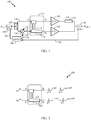
- FIG. 1 illustrates an exemplary embodiment of an improved Doherty power amplifier 100 for millimeter (MM) wave applications.
- the amplifier 100 is suitable for use in a wireless handset or other portable device and also for use in a base station or any other wireless communication apparatus.
- the amplifier 100 comprises a power splitter 102 that receives a MM wave input signal (P IN ).
- a power detector 104 detects power on the input and provides a detection signal 106 to a controller 108.
- a first output (split signal) 110 of the splitter 102 is input to the "A" input of a hybrid plus coupler 112.
- a second output (split signal) 114 of the splitter 102 is input to a phase shifter 116.
- the phase shifted output signal 132 of the phase shifter 116 is a phase shifted version of the second split signal 114 and is input to the "C" input of the hybrid plus coupler 112. Both outputs of the splitter 102 have power levels that are 3dB less than the input signal (P IN ) power level.
- the hybrid plus coupler 112 comprises a 1 ⁇ 4 wavelength extension 118.
- This extension is used to provide a 90 degree phase shift.
- the extension 118 can be constructed by distributed elements, like transmission lines, or using lumped elements, like LC filters.
- the hybrid plus coupler 108 comprise a 180 degree ring coupler as discussed below.
- the hybrid plus coupler 112 has a first output at terminal "B” coupled to a main power amplifier (PA1) 120 and a second output at terminal “D” coupled to an auxiliary power amplifier (PA2) 122.
- the output of the first power amplifier 120 is input to a (1 ⁇ 4 wavelength phase shifter) 124 that is used to equalize the total phase shift from P IN to P OUT between the PA1 signal path and the PA2 signal path.
- the output of the phase shifter 124 and second power amplifier 122 are coupled together to produce the output power signal (P OUT ).
- the hybrid plus coupler 112 generates first and second combinations of the phase shifted version signal 132 and the millimeter wave second signal 110.
- the combinations of the input signals are provided at first and second output terminals (B and D), respectively.
- the first and second combinations set output power levels at the first and second output terminals, which in effect, distributes the input power on the hybrid coupler input terminals to its output terminals based on the phase shift introduced by the phase shifter 116.
- the controller 108 outputs a phase control signal 126 to control the amount of phase shift applied by the phase shifter 116 based on the power detection signal 106 detected by the power detector 104.
- the controller 108 controls the phase shifter 116 to generate a phase shift such that the hybrid plus coupler 112 directs power to the main power amplifier 120 and away from the auxiliary power amplifier 122, thereby providing improved efficiency over conventional systems.
- a power detector 128 is coupled to detect the power level of the output signal (P OUT ) and provide a detected power signal 130 to the controller 108.
- the controller 108 operates to control the phase shift provided by the phase shifter 116 based on the detected power signal 130.
- the extension 118 assists in distributing the power based on the phase shift introduced by the phase shifter 116.
- an improved Doherty amplifier comprises a hybrid plus coupler 112 to steer the input power distribution with the phase shifter 116 and therefore provide greater efficiency at low power.
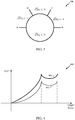
- FIG. 2 shows an exemplary embodiment of a hybrid plus coupler 200 .
- the hybrid plus coupler 200 is suitable for use as the hybrid plus coupler 108 shown in FIG. 1 .
- the hybrid plus coupler 200 comprises input terminals A and C and output terminals B and D.
- the hybrid plus coupler 200 also comprises extension 202 which is used to provide a 90 degree phase shift.
- the extension 202 can be constructed by distributed elements, like transmission lines, or using lumped elements, like LC filters. A phase difference between the signals on the input terminals (A and C) results in the input power being redistributed on the output terminals (B and D).
- FIG. 3 shows an exemplary embodiment of a hybrid ring coupler 300, which is not covered by the claimed invention.
- the hybrid ring coupler 300 is suitable for use as the hybrid plus coupler 108 shown in FIG. 1 .
- the hybrid ring coupler 300 comprises inputs A and C and outputs B and D. A phase difference between the signals at the input terminals (A and C) results in power being redistributed on the output terminals (B and D).
- FIG. 4 shows an exemplary graph 400 that illustrates the increase in efficiency provided by exemplary embodiments of the improved Doherty amplifier 100.
- the graph 400 includes plot line 402 representing the efficiency of a typical Doherty amplifier.
- FIG. 5 shows an exemplary method 500 for providing an improved Doherty amplifier.
- the method 500 is performed by the amplifier 100 shown in FIG. 1 .
- a MM wave signal to be amplified is input to a power splitter to generate first and second split signals.
- the signal is input to the power splitter 102 shown in FIG. 1 to generate the first split signal 110 and the second split signal 114.
- the second split signal is phase shifted to generate a phase shifted split signal.
- the split signal 114 is input into the phase shifter 116 to generate the phase shifted signal 132.
- first and second combinations of the phase shifted version of the first signal and a millimeter wave second signal are generated at first and second output terminals, respectively.
- the first and second combinations set output power levels at the first and second output terminals.
- the first split signal and the phase shifted split signal are input to the hybrid plus coupler 112.
- the signal 110 and the signal 132 are input to the input terminals (A and C) of the hybrid plus coupler 112.
- the hybrid plus coupler 112 has extension 118 to provide a 90 degree phase shift as described above.
- the hybrid plus coupler operates to generate combinations of its input signals according to the equations shown above.
- the hybrid plus coupler operates to adjust output power levels at its output terminals based on combinations of a phase shifted first MM wave signal and a second MM wave signal.
- a power level is detected.
- the power detector 104 detects the power of the input signal and provides the power detection signal 106 to the controller 108.
- the power detector 128 detects the power of the output signal (P OUT ) and provides the power detection signal 130 to the controller 108.
- a phase shift is adjusted based on the detected power to improve efficiency.
- the controller 108 outputs the phase control signal 126 to control the phase shift introduced by the phase shifter 116 so that the power distribution provided by the hybrid plus coupler 112 provides improved efficiency over conventional systems.
- the method 500 operates to provide an improved Doherty amplifier using the phase shifter 116 and hybrid plus coupler 112 to adjust the power distribution of the output to achieve improved efficiency.
- the operations of the method 500 may be rearranged or modified to provide the functions described herein.
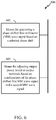
- FIG. 6 shows an exemplary embodiment of a Doherty amplifier apparatus 600 that provides improved efficiency.
- the apparatus 600 is suitable for use as the amplifier 100 shown in FIG. 1 .
- the apparatus 600 is implemented by one or more modules configured to provide the functions as described herein.
- each module comprises hardware and/or hardware executing software.
- the apparatus 600 comprises a first module comprising means (602) for generating a phase shifted first millimeter (MM) wave signal based on a selected phase shift, which in an aspect comprises phase shifter 116.
- MM millimeter
- the apparatus 600 also comprises a second module comprising means (604) for adjusting output power levels at output terminals based on combinations of the phase shifted first MM wave signal and a second MM wave signal, which in an aspect comprises the hybrid plus coupler 112.
- transistor types and technologies may be substituted, rearranged or otherwise modified to achieve the same results.
- circuits shown utilizing PMOS transistors may be modified to use NMOS transistors and vice versa.
- the amplifiers disclosed herein may be realized using a variety of transistor types and technologies and are not limited to those transistor types and technologies illustrated in the Drawings.
- transistors types such as BJT, GaAs, MOSFET or any other transistor technology may be used.
- DSP Digital Signal Processor
- ASIC Application Specific Integrated Circuit
- FPGA Field Programmable Gate Array
- a general purpose processor may be a microprocessor, but in the alternative, the processor may be any conventional processor, controller, microcontroller, or state machine.
- a processor may also be implemented as a combination of computing devices, e.g., a combination of a DSP and a microprocessor, a plurality of microprocessors, one or more microprocessors in conjunction with a DSP core, or any other such configuration.
- a software module may reside in Random Access Memory (RAM), flash memory, Read Only Memory (ROM), Electrically Programmable ROM (EPROM), Electrically Erasable Programmable ROM (EEPROM), registers, hard disk, a removable disk, a CD-ROM, or any other form of storage medium known in the art.
- An exemplary storage medium is coupled to the processor such that the processor can read information from, and write information to, the storage medium.
- the storage medium may be integral to the processor.
- the processor and the storage medium may reside in an ASIC.
- the ASIC may reside in a user terminal.
- the processor and the storage medium may reside as discrete components in a user terminal.
- the functions described may be implemented in hardware, software, firmware, or any combination thereof. If implemented in software, the functions may be stored on or transmitted over as one or more instructions or code on a computer-readable medium.
- Computer-readable media includes both non-transitory computer storage media and communication media including any medium that facilitates transfer of a computer program from one place to another.
- a non-transitory storage media may be any available media that can be accessed by a computer.
- such computer-readable media can comprise RAM, ROM, EEPROM, CD-ROM or other optical disk storage, magnetic disk storage or other magnetic storage devices, or any other medium that can be used to carry or store desired program code in the form of instructions or data structures and that can be accessed by a computer.
- any connection is properly termed a computer-readable medium.
- the software is transmitted from a website, server, or other remote source using a coaxial cable, fiber optic cable, twisted pair, digital subscriber line (DSL), or wireless technologies such as infrared, radio, and microwave
- the coaxial cable, fiber optic cable, twisted pair, DSL, or wireless technologies such as infrared, radio, and microwave are included in the definition of medium.
- Disk and disc includes compact disc (CD), laser disc, optical disc, digital versatile disc (DVD), floppy disk and blu-ray disc where disks usually reproduce data magnetically, while discs reproduce data optically with lasers. Combinations of the above should also be included within the scope of computer-readable media.
Landscapes
- Engineering & Computer Science (AREA)
- Power Engineering (AREA)
- Physics & Mathematics (AREA)
- Nonlinear Science (AREA)
- Amplifiers (AREA)
- Microwave Amplifiers (AREA)
Claims (10)
- Ein Verfahren zu Leistungsverstärkung in einer Vorrichtung, das Folgendes aufweist:Splitten bzw. Aufteilen (502) eines Millimeterwelleneingangssignals bzw. MM-Wellen-Eingangssignals zum Generieren eines ersten MM-Wellen-Signals und eines zweiten MM-Wellen-Signals,Generieren eines phasenverschobenen ersten MM-Wellen-Signals basierend auf einer ausgewählten Phasenverschiebung (504) und dem ersten MM-Wellen-Signal;Vorsehen von intermediären Ausgangsleistungspegeln an ersten und zweiten Ausgangsanschlüssen (B, D) eines hybriden Kopplungselementes basierend auf Kombinationen des phasenverschobenen ersten MM-Wellen-Signals und des zweiten MM-Wellen-Signals (506), wobei das hybride Kopplungselement eine 1/4-Wellenlängen-Erweiterung (118) aufweist, die eine 90-Grad-Phasenverschiebung an dem zweiten Ausgangsanschluss (D) des hybriden Kopplungselementes vorsieht, undwobei der erste Ausgangsanschluss (B) des hybriden Kopplungselementes an einen Eingang eines ersten Leistungsverstärkers (PA1) gekoppelt ist, und der zweite Ausgangsanschluss (D) des hybriden Kopplungselementes an einen Eingang eines zweiten Leistungsverstärkers (PA2) gekoppelt ist; undAnpassen der intermediären Ausgangsleistungspegel durch Anpassen der ausgewählten Phasenverschiebung, wobei die ausgewählte Phasenverschiebung basierend auf einem detektierten Ausgangsleistungspegel der Vorrichtung (508, 510) angepasst wird.
- Verfahren nach Anspruch 1, das Folgendes aufweist:Vorsehen von intermediärer Ausgangsleistung an dem ersten Ausgangsanschluss (B) basierend auf einer ersten Kombination; undVorsehen von intermediärer Ausgangsleistung an dem zweiten Ausgangsanschluss (D) basierend auf einer zweiten Kombination.
- Verfahren nach Anspruch 1, wobei das erste MM-Wellen-Signale und das zweite MM-Wellen-Signal auf im Wesentlichen gleichen Leistungspegeln (502) sind.
- Verfahren nach Anspruch 1, das weiter Generieren einer Leistungsverteilung zwischen dem ersten Ausgangsanschluss (B) und dem zweiten Ausgangsanschluss (D) basierend auf einer Phasendifferenz (ϕ) zwischen dem zweiten MM-Wellen-Signal und dem phasenverschobenen ersten MM-Wellen-Signal aufweist, wobei die Leistungsverteilung zwischen den ersten und zweiten Ausgangsanschlüssen (B, D) bestimmt wird aus:


- Eine Vorrichtung zu Leistungsverstärkung, die Folgendes aufweist:Mittel zum Splitten bzw. Aufteilen (102) eines Millimeterwelleneingangssignals bzw. MM-Wellen-Eingangssignals zum Generieren eines ersten MM-Wellen-Signals und eines zweiten MM-Wellen-Signals,Mittel zum Generieren (116) eines phasenverschobenen ersten MM-Wellen-Signals (132) basierend auf einer ausgewählten Phasenverschiebung und dem ersten MM-Wellen-Signal;Mittel zum Vorsehen (112) von intermediären Ausgangsleistungspegeln an ersten und zweiten Ausgangsanschlüssen (B, D) der Mittel zum Vorsehen basierend auf Kombinationen des phasenverschobenen ersten MM-Wellen-Signals (132) und des zweiten MM-Wellen-Signals (110), wobei die Mittel zum Vorsehen (112) ein hybrides Kopplungselement sind, das eine 1/4-Wellenlängen-Erweiterung (118) aufweist, die konfiguriert ist zum Vorsehen einer 90-Grad-Phasenverschiebung an dem zweiten Ausgangsanschluss (D) des hybriden Kopplungselementes, undwobei der erste Ausgangsanschluss (B) des hybriden Kopplungselementes an einen Eingang eines ersten Leistungsverstärkers (PA1) gekoppelt ist, und der zweite Ausgangsanschluss (D) des hybriden Kopplungselementes an einen Eingang eines zweiten Leistungsverstärkers (PA2) gekoppelt ist;Mittel zum Anpassen der intermediären Ausgangsleistungspegel durch Anpassen der ausgewählten Phasenverschiebung, die Mittel aufweisen zum Anpassen der ausgewählten Phasenverschiebung (108) basierend auf einem detektierten Ausgangsleistungspegel (130) der Vorrichtung.
- Vorrichtung nach Anspruch 5, die weiter Folgendes aufweist:Mittel zum Vorsehen von intermediärer Ausgangsleistung an dem ersten Ausgangsanschluss (B) basierend auf einer ersten Kombination; undMittel zum Vorsehen von intermediärer Ausgangsleistung an dem zweiten Ausgangsanschluss (D) basierend auf einer zweiten Kombination.
- Vorrichtung nach Anspruch 5, die weiter Mittel aufweist zum Generieren einer Leistungsverteilung zwischen dem ersten Ausgangsanschluss (B) und dem zweiten Ausgangsanschluss (D) basierend auf einer Phasendifferenz (ϕ) zwischen dem zweiten MM-Wellen-Signal und dem phasenverschobenen ersten MM-Wellen-Signal, wobei die Leistungsverteilung zwischen den ersten und zweiten Ausgangsanschlüssen (B, D) bestimmt wird aus:


- Vorrichtung nach Anspruch 5, wobei die Vorrichtung weiter Mittel aufweist zum Verstärken eines MM-Wellen-Eingangssignals in wenigstens einem von einer Drahtloseinrichtung und einer Basisstation.
- Vorrichtung nach Anspruch 5, wobei die Vorrichtung als ein Doherty-Verstärker konfiguriert ist.
- Vorrichtung nach Anspruch 5, wobei die Mittel zum Aufteilen einen Splitter bzw. ein Aufteilungselement aufweisen, das konfiguriert ist zum Empfangen eines MM-Wellen-Eingangssignals (P_IN) und zum Generieren des ersten MM-Wellen-Signals (114) und des zweiten MM-Wellen-Signals (110) bei im Wesentlichen gleichen Leistungspegeln, wobei das erste MM-Wellen-Signal in die Mittel zum Generieren des phasenverschobenen ersten MM-Wellen-Signals (116) eingegeben wird.
Applications Claiming Priority (2)
| Application Number | Priority Date | Filing Date | Title |
|---|---|---|---|
| US13/424,199 US8970297B2 (en) | 2012-03-19 | 2012-03-19 | Reconfigurable input power distribution doherty amplifier with improved efficiency |
| PCT/US2013/033022 WO2013142529A2 (en) | 2012-03-19 | 2013-03-19 | Reconfigurable input power distribution doherty amplifier with improved efficiency |
Publications (2)
| Publication Number | Publication Date |
|---|---|
| EP2828970A2 EP2828970A2 (de) | 2015-01-28 |
| EP2828970B1 true EP2828970B1 (de) | 2021-03-10 |
Family
ID=48048259
Family Applications (1)
| Application Number | Title | Priority Date | Filing Date |
|---|---|---|---|
| EP13714459.8A Not-in-force EP2828970B1 (de) | 2012-03-19 | 2013-03-19 | Doherty-verstärker mit rekonfigurierbarer eingangsleistungsverteilung und erhöhter effizienz |
Country Status (6)
| Country | Link |
|---|---|
| US (1) | US8970297B2 (de) |
| EP (1) | EP2828970B1 (de) |
| JP (1) | JP6185551B2 (de) |
| KR (1) | KR20140146121A (de) |
| CN (1) | CN104205625B (de) |
| WO (1) | WO2013142529A2 (de) |
Families Citing this family (19)
| Publication number | Priority date | Publication date | Assignee | Title |
|---|---|---|---|---|
| US9306502B2 (en) | 2011-05-09 | 2016-04-05 | Qualcomm Incorporated | System providing switchable impedance transformer matching for power amplifiers |
| US9203348B2 (en) | 2012-01-27 | 2015-12-01 | Freescale Semiconductor, Inc. | Adjustable power splitters and corresponding methods and apparatus |
| US8514007B1 (en) | 2012-01-27 | 2013-08-20 | Freescale Semiconductor, Inc. | Adjustable power splitter and corresponding methods and apparatus |
| US9431969B2 (en) * | 2012-12-11 | 2016-08-30 | Rf Micro Devices, Inc. | Doherty power amplifier with tunable impedance load |
| US9031518B2 (en) | 2012-12-17 | 2015-05-12 | Qualcomm Incorporated | Concurrent hybrid matching network |
| US9397617B2 (en) | 2013-06-25 | 2016-07-19 | Rf Micro Devices, Inc. | Multi-broadband Doherty power amplifier |
| US9948243B2 (en) | 2013-09-30 | 2018-04-17 | Qorvo Us, Inc. | Reconfigurable load modulation amplifier |
| US9484865B2 (en) | 2013-09-30 | 2016-11-01 | Qorvo Us, Inc. | Reconfigurable load modulation amplifier |
| US9225291B2 (en) * | 2013-10-29 | 2015-12-29 | Freescale Semiconductor, Inc. | Adaptive adjustment of power splitter |
| US9369095B2 (en) | 2014-01-27 | 2016-06-14 | Rf Micro Devices, Inc. | Unbalanced linear power amplifier |
| US9774299B2 (en) | 2014-09-29 | 2017-09-26 | Nxp Usa, Inc. | Modifiable signal adjustment devices for power amplifiers and corresponding methods and apparatus |
| US9831837B2 (en) | 2014-11-05 | 2017-11-28 | Qualcomm Incorporated | Dynamic power divider circuits and methods |
| US9647611B1 (en) | 2015-10-28 | 2017-05-09 | Nxp Usa, Inc. | Reconfigurable power splitters and amplifiers, and corresponding methods |
| CN107147366B (zh) * | 2017-06-12 | 2023-08-29 | 广州慧智微电子股份有限公司 | 一种射频功率放大器的温度补偿电路 |
| JP6835262B2 (ja) * | 2018-01-22 | 2021-02-24 | 三菱電機株式会社 | 増幅器 |
| CN109167580B (zh) * | 2018-10-30 | 2022-06-14 | 北京振兴计量测试研究所 | 一种平面四路功率合成放大器 |
| GB201817747D0 (en) * | 2018-10-31 | 2018-12-19 | Leonardo Mw Ltd | A radio frequency power amplifier |
| FR3115113B1 (fr) * | 2020-10-09 | 2023-01-06 | St Microelectronics Sa | Procédé et dispositif de détermination du déphasage entre deux signaux, en particulier des signaux radiofréquence |
| US20250096734A1 (en) * | 2023-09-20 | 2025-03-20 | Qualcomm Incorporated | Phase-Reconfigurable Circuits with Dynamic Phase Modulation for Wideband Dual-Input Power Amplifiers |
Citations (3)
| Publication number | Priority date | Publication date | Assignee | Title |
|---|---|---|---|---|
| JPS53136945A (en) * | 1977-05-06 | 1978-11-29 | Fujitsu Ltd | Parallel-operation amplifier |
| JP2010273212A (ja) * | 2009-05-22 | 2010-12-02 | Sumitomo Electric Ind Ltd | 増幅装置及び無線基地局 |
| WO2011060706A1 (zh) * | 2009-11-18 | 2011-05-26 | 中兴通讯股份有限公司 | 一种功率放大电路实现方法及功率放大装置 |
Family Cites Families (62)
| Publication number | Priority date | Publication date | Assignee | Title |
|---|---|---|---|---|
| US4490684A (en) * | 1983-01-03 | 1984-12-25 | Motorola, Inc. | Adaptive quadrature combining apparatus |
| JPS61265910A (ja) * | 1985-05-20 | 1986-11-25 | Fujitsu Ltd | ハイパワ増幅器 |
| US5287069A (en) * | 1990-02-07 | 1994-02-15 | Fujitsu Limited | Constant-amplitude wave combination type amplifier |
| JPH04288703A (ja) * | 1991-02-01 | 1992-10-13 | Fujitsu Ltd | 吸収抵抗内蔵型ラットレース及び増幅器 |
| JPH06120750A (ja) * | 1992-10-01 | 1994-04-28 | Nec Corp | 電力増幅装置 |
| JP2001203540A (ja) * | 2000-01-19 | 2001-07-27 | Hitachi Ltd | 高周波電力増幅器 |
| SE520760C2 (sv) | 2000-06-06 | 2003-08-19 | Ericsson Telefon Ab L M | Doherty-förstärkare av flerstegstyp |
| US6639463B1 (en) * | 2000-08-24 | 2003-10-28 | Lucent Technologies Inc. | Adaptive power amplifier system and method |
| US6384679B1 (en) | 2000-11-15 | 2002-05-07 | National Semiconductor Corporation | Rail-to-rail amplifier with reduced GM and compensating cap |
| US6472934B1 (en) * | 2000-12-29 | 2002-10-29 | Ericsson Inc. | Triple class E Doherty amplifier topology for high efficiency signal transmitters |
| JP3809777B2 (ja) | 2001-05-30 | 2006-08-16 | ソニー株式会社 | 電力増幅器 |
| US6522160B1 (en) | 2001-06-13 | 2003-02-18 | Micron Technology, Inc. | Input buffer with automatic switching point adjustment circuitry, and synchronous DRAM device including same |
| JP3947373B2 (ja) | 2001-07-31 | 2007-07-18 | 株式会社ルネサステクノロジ | 高周波電力増幅器 |
| US6806767B2 (en) | 2002-07-09 | 2004-10-19 | Anadigics, Inc. | Power amplifier with load switching circuit |
| KR100450744B1 (ko) | 2002-08-29 | 2004-10-01 | 학교법인 포항공과대학교 | 도허티 증폭기 |
| US6794935B2 (en) | 2002-10-17 | 2004-09-21 | Motorola Inc. | Power amplification circuit and method for supplying power at a plurality of desired power output levels |
| JP2004221646A (ja) | 2003-01-09 | 2004-08-05 | Nec Corp | ドハ−ティ増幅器 |
| DE10308848A1 (de) | 2003-02-27 | 2004-09-09 | Marconi Communications Gmbh | Integrierte Verstärkeranordnung |
| JP3907052B2 (ja) | 2003-03-07 | 2007-04-18 | ソニー・エリクソン・モバイルコミュニケーションズ株式会社 | 通信端末装置及び増幅回路 |
| US6922102B2 (en) * | 2003-03-28 | 2005-07-26 | Andrew Corporation | High efficiency amplifier |
| US7444124B1 (en) | 2003-05-14 | 2008-10-28 | Marvell International Ltd. | Adjustable segmented power amplifier |
| TW200518345A (en) | 2003-08-08 | 2005-06-01 | Renesas Tech Corp | Semiconductor device |
| US20050134377A1 (en) | 2003-12-23 | 2005-06-23 | Dent Paul W. | Doherty amplifier |
| US7157965B1 (en) | 2004-06-21 | 2007-01-02 | Qualcomm Incorporated | Summing power amplifier |
| CN100542011C (zh) | 2004-06-29 | 2009-09-16 | Nxp股份有限公司 | 具有高功效的集成多赫尔蒂型放大器装置 |
| JP4715994B2 (ja) | 2004-08-26 | 2011-07-06 | 日本電気株式会社 | ドハティ増幅器並列運転回路 |
| US20060105733A1 (en) | 2004-11-16 | 2006-05-18 | Singh Donald R | System and method for developing ultra-sensitive microwave and millimeter wave phase discriminators |
| US7295065B2 (en) | 2004-11-18 | 2007-11-13 | Beecem Communications Inc. | High efficiency doherty amplifier with a segmented main amplifier |
| WO2006066461A1 (en) | 2004-12-24 | 2006-06-29 | Huawei Technologies Co., Ltd. | Butler doherty power amplifier |
| CN101180792A (zh) | 2005-05-20 | 2008-05-14 | Nxp股份有限公司 | 高功率效率的集成多赫尔蒂型放大器结构 |
| US7183843B1 (en) * | 2005-06-27 | 2007-02-27 | Rockwell Collins, Inc. | Electronically tuned power amplifier |
| KR100752280B1 (ko) | 2005-12-14 | 2007-08-28 | 삼성전자주식회사 | 휴대단말기의 안테나주파수 자동매칭 장치 |
| DE102006008790A1 (de) * | 2006-02-24 | 2007-09-06 | Infineon Technologies Ag | Modulationseinrichtung für einen Sendepfad, Verfahren zur Signalverarbeitung in einem Sendepfad und Sendepfad mit der Modulationseinrichtung |
| US7719141B2 (en) | 2006-11-16 | 2010-05-18 | Star Rf, Inc. | Electronic switch network |
| US8245179B2 (en) | 2006-11-21 | 2012-08-14 | Nec Corporation | RF circuit, circuit evaluation method, algorithm and recording medium |
| US7561854B2 (en) | 2006-12-01 | 2009-07-14 | Harris Corporation | Lossless transmit path antenna switch circuit |
| KR100814415B1 (ko) | 2007-02-14 | 2008-03-18 | 포항공과대학교 산학협력단 | 하모닉 제어 회로를 이용한 고효율 도허티 전력 증폭기 |
| US20080207256A1 (en) | 2007-02-22 | 2008-08-28 | Texas Instruments Incorporated | Concurrent impedance matching of a wireless transceiver |
| JP5474764B2 (ja) * | 2007-04-23 | 2014-04-16 | ダリ システムズ カンパニー リミテッド | Nウェイ分散電力増幅器 |
| EP2191567A1 (de) | 2007-09-03 | 2010-06-02 | Nxp B.V. | Mehrband-doherty-verstärker |
| US7609115B2 (en) | 2007-09-07 | 2009-10-27 | Raytheon Company | Input circuitry for transistor power amplifier and method for designing such circuitry |
| KR20090071834A (ko) | 2007-12-28 | 2009-07-02 | 성균관대학교산학협력단 | 고조파 동조를 이용한 도허티 증폭기 |
| KR101547818B1 (ko) | 2008-01-29 | 2015-08-27 | 삼성전자주식회사 | 시분할복신 무선통신시스템에서 송수신 안테나 스위칭 장치 |
| US8103221B2 (en) | 2008-05-30 | 2012-01-24 | National Ict Australia Limited | High-isolation transmit/receive switch on CMOS for millimeter-wave applications |
| JP2009303040A (ja) | 2008-06-16 | 2009-12-24 | Toshiba Corp | 高周波電力増幅器、および増幅方法 |
| US9300508B2 (en) | 2008-08-07 | 2016-03-29 | Trex Enterprises Corp. | High data rate milllimeter wave radio on a chip |
| US7952433B2 (en) | 2008-11-25 | 2011-05-31 | Samsung Electro-Mechanics Company | Power amplifiers with discrete power control |
| US7863979B2 (en) | 2009-01-26 | 2011-01-04 | Skyworks Solutions, Inc. | High efficiency power amplifier having embedded switching |
| US8666340B2 (en) | 2009-03-03 | 2014-03-04 | Broadcom Corporation | Method and system for on-chip impedance control to impedance match a configurable front end |
| JP5163577B2 (ja) | 2009-03-27 | 2013-03-13 | 富士通株式会社 | 増幅回路及び送受信機 |
| US8432237B2 (en) | 2009-05-21 | 2013-04-30 | Qualcomm, Incorporated | Output circuit with integrated impedance matching, power combining and filtering for power amplifiers and other circuits |
| KR101573719B1 (ko) | 2009-07-31 | 2015-12-02 | 삼성전자주식회사 | 시분할 복신 방식의 무선통신시스템에서 수신회로 보호 장치 및 방법 |
| US8295212B2 (en) | 2009-08-05 | 2012-10-23 | Alcatel Lucent | System and method for TDD/TMA with hybrid bypass switch of receiving amplifier |
| WO2011045312A1 (en) | 2009-10-12 | 2011-04-21 | St-Ericsson (France) Sas | Integrated transformer with multiple transformation ratios |
| CN102577104B (zh) | 2009-10-23 | 2015-01-14 | 日本碍子株式会社 | 多赫蒂放大器用合成器 |
| EP2339745A1 (de) | 2009-12-15 | 2011-06-29 | Nxp B.V. | Doherty-Verstärker |
| US9048787B2 (en) | 2010-04-20 | 2015-06-02 | Rf Micro Devices, Inc. | Combined RF detector and RF attenuator with concurrent outputs |
| US8626084B2 (en) | 2010-05-13 | 2014-01-07 | Qualcomm, Incorporated | Area efficient concurrent matching transceiver |
| US8760240B2 (en) | 2010-09-15 | 2014-06-24 | Wilocity, Ltd. | Method for designing coupling-function based millimeter wave electrical elements |
| US8611834B2 (en) | 2010-11-01 | 2013-12-17 | Cree, Inc. | Matching network for transmission circuitry |
| US9306502B2 (en) | 2011-05-09 | 2016-04-05 | Qualcomm Incorporated | System providing switchable impedance transformer matching for power amplifiers |
| US9031518B2 (en) | 2012-12-17 | 2015-05-12 | Qualcomm Incorporated | Concurrent hybrid matching network |
-
2012
- 2012-03-19 US US13/424,199 patent/US8970297B2/en active Active
-
2013
- 2013-03-19 EP EP13714459.8A patent/EP2828970B1/de not_active Not-in-force
- 2013-03-19 CN CN201380014736.8A patent/CN104205625B/zh not_active Expired - Fee Related
- 2013-03-19 JP JP2015501863A patent/JP6185551B2/ja not_active Expired - Fee Related
- 2013-03-19 KR KR1020147029063A patent/KR20140146121A/ko not_active Withdrawn
- 2013-03-19 WO PCT/US2013/033022 patent/WO2013142529A2/en not_active Ceased
Patent Citations (3)
| Publication number | Priority date | Publication date | Assignee | Title |
|---|---|---|---|---|
| JPS53136945A (en) * | 1977-05-06 | 1978-11-29 | Fujitsu Ltd | Parallel-operation amplifier |
| JP2010273212A (ja) * | 2009-05-22 | 2010-12-02 | Sumitomo Electric Ind Ltd | 増幅装置及び無線基地局 |
| WO2011060706A1 (zh) * | 2009-11-18 | 2011-05-26 | 中兴通讯股份有限公司 | 一种功率放大电路实现方法及功率放大装置 |
Also Published As
| Publication number | Publication date |
|---|---|
| US8970297B2 (en) | 2015-03-03 |
| CN104205625B (zh) | 2017-06-20 |
| WO2013142529A2 (en) | 2013-09-26 |
| EP2828970A2 (de) | 2015-01-28 |
| KR20140146121A (ko) | 2014-12-24 |
| JP2015514360A (ja) | 2015-05-18 |
| CN104205625A (zh) | 2014-12-10 |
| JP6185551B2 (ja) | 2017-08-23 |
| WO2013142529A3 (en) | 2013-11-14 |
| US20130241640A1 (en) | 2013-09-19 |
Similar Documents
| Publication | Publication Date | Title |
|---|---|---|
| EP2828970B1 (de) | Doherty-verstärker mit rekonfigurierbarer eingangsleistungsverteilung und erhöhter effizienz | |
| CN102197584B (zh) | 功率放大器及其放大方法 | |
| KR101126054B1 (ko) | 차동 입력을 갖는 직교위상 출력 저잡음 트랜스컨덕턴스 증폭기 | |
| EP2579456B1 (de) | Steuerungsverfahren für eine schnell mitlaufende stromquelle, schnell mitlaufende stromquelle und system damit | |
| US20130163789A1 (en) | Amplifier and amplifying method | |
| JP4754019B2 (ja) | Mimo送信装置 | |
| US8115546B2 (en) | Apparatus and method for maximizing performance of peaking amplifier in doherty amplifier | |
| EP2451074B1 (de) | Verstärker | |
| US9438187B2 (en) | Amplifying device, transmitting device | |
| CN101401261A (zh) | 功率放大器控制器电路 | |
| EP2963810B1 (de) | Doherty-leistungsverstärkerschaltung und leistungsverstärker | |
| JP2016063543A (ja) | ベース電流を再使用する増幅器 | |
| US20100295620A1 (en) | High-speed, multi-stage class ab amplifiers | |
| EP2634916A1 (de) | Doherty-Verstärker | |
| US20140266464A1 (en) | Apparatus and Method for Asymmetrically Driven Partial Outphasing Power Amplifier | |
| US8952754B2 (en) | Linearization of heterogeneous power amplifier systems | |
| EP2538548B1 (de) | Verfahren und vorrichtung zur steuerung eines spitzenverstärkers und doherty-leistungsverstärker | |
| JP5331732B2 (ja) | エンベロープトラッキング電力増幅器およびエンベロープトラッキング増幅方法 | |
| US20150054581A1 (en) | Combination nmos/pmos power amplifier | |
| CN112564647B (zh) | 一种功率放大器及功率放大方法、存储介质 | |
| KR101500570B1 (ko) | 비대칭 도허티 전력 증폭기 | |
| Sim et al. | A CMOS power amplifier using a split cascode structure to enhance its efficiency | |
| JP2011211655A (ja) | 高周波増幅器 | |
| US9106198B2 (en) | High power tunable capacitor | |
| WO2015131385A1 (en) | Method and apparatus for modulating power supply |
Legal Events
| Date | Code | Title | Description |
|---|---|---|---|
| PUAI | Public reference made under article 153(3) epc to a published international application that has entered the european phase |
Free format text: ORIGINAL CODE: 0009012 |
|
| 17P | Request for examination filed |
Effective date: 20141014 |
|
| AK | Designated contracting states |
Kind code of ref document: A2 Designated state(s): AL AT BE BG CH CY CZ DE DK EE ES FI FR GB GR HR HU IE IS IT LI LT LU LV MC MK MT NL NO PL PT RO RS SE SI SK SM TR |
|
| AX | Request for extension of the european patent |
Extension state: BA ME |
|
| DAX | Request for extension of the european patent (deleted) | ||
| STAA | Information on the status of an ep patent application or granted ep patent |
Free format text: STATUS: EXAMINATION IS IN PROGRESS |
|
| 17Q | First examination report despatched |
Effective date: 20181219 |
|
| GRAP | Despatch of communication of intention to grant a patent |
Free format text: ORIGINAL CODE: EPIDOSNIGR1 |
|
| STAA | Information on the status of an ep patent application or granted ep patent |
Free format text: STATUS: GRANT OF PATENT IS INTENDED |
|
| RIC1 | Information provided on ipc code assigned before grant |
Ipc: H03F 3/189 20060101ALI20200915BHEP Ipc: H03F 1/02 20060101AFI20200915BHEP |
|
| INTG | Intention to grant announced |
Effective date: 20201006 |
|
| GRAS | Grant fee paid |
Free format text: ORIGINAL CODE: EPIDOSNIGR3 |
|
| GRAA | (expected) grant |
Free format text: ORIGINAL CODE: 0009210 |
|
| STAA | Information on the status of an ep patent application or granted ep patent |
Free format text: STATUS: THE PATENT HAS BEEN GRANTED |
|
| AK | Designated contracting states |
Kind code of ref document: B1 Designated state(s): AL AT BE BG CH CY CZ DE DK EE ES FI FR GB GR HR HU IE IS IT LI LT LU LV MC MK MT NL NO PL PT RO RS SE SI SK SM TR |
|
| REG | Reference to a national code |
Ref country code: GB Ref legal event code: FG4D |
|
| REG | Reference to a national code |
Ref country code: AT Ref legal event code: REF Ref document number: 1370950 Country of ref document: AT Kind code of ref document: T Effective date: 20210315 Ref country code: CH Ref legal event code: EP |
|
| REG | Reference to a national code |
Ref country code: IE Ref legal event code: FG4D |
|
| REG | Reference to a national code |
Ref country code: DE Ref legal event code: R096 Ref document number: 602013076162 Country of ref document: DE |
|
| PGFP | Annual fee paid to national office [announced via postgrant information from national office to epo] |
Ref country code: FR Payment date: 20210310 Year of fee payment: 9 |
|
| PGFP | Annual fee paid to national office [announced via postgrant information from national office to epo] |
Ref country code: DE Payment date: 20210219 Year of fee payment: 9 Ref country code: GB Payment date: 20210310 Year of fee payment: 9 |
|
| REG | Reference to a national code |
Ref country code: LT Ref legal event code: MG9D |
|
| PG25 | Lapsed in a contracting state [announced via postgrant information from national office to epo] |
Ref country code: HR Free format text: LAPSE BECAUSE OF FAILURE TO SUBMIT A TRANSLATION OF THE DESCRIPTION OR TO PAY THE FEE WITHIN THE PRESCRIBED TIME-LIMIT Effective date: 20210310 Ref country code: GR Free format text: LAPSE BECAUSE OF FAILURE TO SUBMIT A TRANSLATION OF THE DESCRIPTION OR TO PAY THE FEE WITHIN THE PRESCRIBED TIME-LIMIT Effective date: 20210611 Ref country code: FI Free format text: LAPSE BECAUSE OF FAILURE TO SUBMIT A TRANSLATION OF THE DESCRIPTION OR TO PAY THE FEE WITHIN THE PRESCRIBED TIME-LIMIT Effective date: 20210310 Ref country code: LT Free format text: LAPSE BECAUSE OF FAILURE TO SUBMIT A TRANSLATION OF THE DESCRIPTION OR TO PAY THE FEE WITHIN THE PRESCRIBED TIME-LIMIT Effective date: 20210310 Ref country code: BG Free format text: LAPSE BECAUSE OF FAILURE TO SUBMIT A TRANSLATION OF THE DESCRIPTION OR TO PAY THE FEE WITHIN THE PRESCRIBED TIME-LIMIT Effective date: 20210610 Ref country code: NO Free format text: LAPSE BECAUSE OF FAILURE TO SUBMIT A TRANSLATION OF THE DESCRIPTION OR TO PAY THE FEE WITHIN THE PRESCRIBED TIME-LIMIT Effective date: 20210610 |
|
| REG | Reference to a national code |
Ref country code: AT Ref legal event code: MK05 Ref document number: 1370950 Country of ref document: AT Kind code of ref document: T Effective date: 20210310 |
|
| REG | Reference to a national code |
Ref country code: NL Ref legal event code: MP Effective date: 20210310 |
|
| PG25 | Lapsed in a contracting state [announced via postgrant information from national office to epo] |
Ref country code: SE Free format text: LAPSE BECAUSE OF FAILURE TO SUBMIT A TRANSLATION OF THE DESCRIPTION OR TO PAY THE FEE WITHIN THE PRESCRIBED TIME-LIMIT Effective date: 20210310 Ref country code: RS Free format text: LAPSE BECAUSE OF FAILURE TO SUBMIT A TRANSLATION OF THE DESCRIPTION OR TO PAY THE FEE WITHIN THE PRESCRIBED TIME-LIMIT Effective date: 20210310 Ref country code: LV Free format text: LAPSE BECAUSE OF FAILURE TO SUBMIT A TRANSLATION OF THE DESCRIPTION OR TO PAY THE FEE WITHIN THE PRESCRIBED TIME-LIMIT Effective date: 20210310 |
|
| PG25 | Lapsed in a contracting state [announced via postgrant information from national office to epo] |
Ref country code: NL Free format text: LAPSE BECAUSE OF FAILURE TO SUBMIT A TRANSLATION OF THE DESCRIPTION OR TO PAY THE FEE WITHIN THE PRESCRIBED TIME-LIMIT Effective date: 20210310 |
|
| PG25 | Lapsed in a contracting state [announced via postgrant information from national office to epo] |
Ref country code: SM Free format text: LAPSE BECAUSE OF FAILURE TO SUBMIT A TRANSLATION OF THE DESCRIPTION OR TO PAY THE FEE WITHIN THE PRESCRIBED TIME-LIMIT Effective date: 20210310 Ref country code: AT Free format text: LAPSE BECAUSE OF FAILURE TO SUBMIT A TRANSLATION OF THE DESCRIPTION OR TO PAY THE FEE WITHIN THE PRESCRIBED TIME-LIMIT Effective date: 20210310 Ref country code: CZ Free format text: LAPSE BECAUSE OF FAILURE TO SUBMIT A TRANSLATION OF THE DESCRIPTION OR TO PAY THE FEE WITHIN THE PRESCRIBED TIME-LIMIT Effective date: 20210310 Ref country code: EE Free format text: LAPSE BECAUSE OF FAILURE TO SUBMIT A TRANSLATION OF THE DESCRIPTION OR TO PAY THE FEE WITHIN THE PRESCRIBED TIME-LIMIT Effective date: 20210310 |
|
| REG | Reference to a national code |
Ref country code: CH Ref legal event code: PL |
|
| PG25 | Lapsed in a contracting state [announced via postgrant information from national office to epo] |
Ref country code: RO Free format text: LAPSE BECAUSE OF FAILURE TO SUBMIT A TRANSLATION OF THE DESCRIPTION OR TO PAY THE FEE WITHIN THE PRESCRIBED TIME-LIMIT Effective date: 20210310 Ref country code: IS Free format text: LAPSE BECAUSE OF FAILURE TO SUBMIT A TRANSLATION OF THE DESCRIPTION OR TO PAY THE FEE WITHIN THE PRESCRIBED TIME-LIMIT Effective date: 20210710 Ref country code: SK Free format text: LAPSE BECAUSE OF FAILURE TO SUBMIT A TRANSLATION OF THE DESCRIPTION OR TO PAY THE FEE WITHIN THE PRESCRIBED TIME-LIMIT Effective date: 20210310 Ref country code: ES Free format text: LAPSE BECAUSE OF FAILURE TO SUBMIT A TRANSLATION OF THE DESCRIPTION OR TO PAY THE FEE WITHIN THE PRESCRIBED TIME-LIMIT Effective date: 20210310 Ref country code: PT Free format text: LAPSE BECAUSE OF FAILURE TO SUBMIT A TRANSLATION OF THE DESCRIPTION OR TO PAY THE FEE WITHIN THE PRESCRIBED TIME-LIMIT Effective date: 20210712 Ref country code: PL Free format text: LAPSE BECAUSE OF FAILURE TO SUBMIT A TRANSLATION OF THE DESCRIPTION OR TO PAY THE FEE WITHIN THE PRESCRIBED TIME-LIMIT Effective date: 20210310 |
|
| REG | Reference to a national code |
Ref country code: DE Ref legal event code: R097 Ref document number: 602013076162 Country of ref document: DE |
|
| REG | Reference to a national code |
Ref country code: BE Ref legal event code: MM Effective date: 20210331 |
|
| PLBE | No opposition filed within time limit |
Free format text: ORIGINAL CODE: 0009261 |
|
| STAA | Information on the status of an ep patent application or granted ep patent |
Free format text: STATUS: NO OPPOSITION FILED WITHIN TIME LIMIT |
|
| PG25 | Lapsed in a contracting state [announced via postgrant information from national office to epo] |
Ref country code: MC Free format text: LAPSE BECAUSE OF FAILURE TO SUBMIT A TRANSLATION OF THE DESCRIPTION OR TO PAY THE FEE WITHIN THE PRESCRIBED TIME-LIMIT Effective date: 20210310 Ref country code: LU Free format text: LAPSE BECAUSE OF NON-PAYMENT OF DUE FEES Effective date: 20210319 Ref country code: LI Free format text: LAPSE BECAUSE OF NON-PAYMENT OF DUE FEES Effective date: 20210331 Ref country code: AL Free format text: LAPSE BECAUSE OF FAILURE TO SUBMIT A TRANSLATION OF THE DESCRIPTION OR TO PAY THE FEE WITHIN THE PRESCRIBED TIME-LIMIT Effective date: 20210310 Ref country code: CH Free format text: LAPSE BECAUSE OF NON-PAYMENT OF DUE FEES Effective date: 20210331 Ref country code: DK Free format text: LAPSE BECAUSE OF FAILURE TO SUBMIT A TRANSLATION OF THE DESCRIPTION OR TO PAY THE FEE WITHIN THE PRESCRIBED TIME-LIMIT Effective date: 20210310 Ref country code: IE Free format text: LAPSE BECAUSE OF NON-PAYMENT OF DUE FEES Effective date: 20210319 |
|
| 26N | No opposition filed |
Effective date: 20211213 |
|
| PG25 | Lapsed in a contracting state [announced via postgrant information from national office to epo] |
Ref country code: SI Free format text: LAPSE BECAUSE OF FAILURE TO SUBMIT A TRANSLATION OF THE DESCRIPTION OR TO PAY THE FEE WITHIN THE PRESCRIBED TIME-LIMIT Effective date: 20210310 |
|
| PG25 | Lapsed in a contracting state [announced via postgrant information from national office to epo] |
Ref country code: IT Free format text: LAPSE BECAUSE OF FAILURE TO SUBMIT A TRANSLATION OF THE DESCRIPTION OR TO PAY THE FEE WITHIN THE PRESCRIBED TIME-LIMIT Effective date: 20210310 |
|
| PG25 | Lapsed in a contracting state [announced via postgrant information from national office to epo] |
Ref country code: IS Free format text: LAPSE BECAUSE OF FAILURE TO SUBMIT A TRANSLATION OF THE DESCRIPTION OR TO PAY THE FEE WITHIN THE PRESCRIBED TIME-LIMIT Effective date: 20210710 |
|
| PG25 | Lapsed in a contracting state [announced via postgrant information from national office to epo] |
Ref country code: BE Free format text: LAPSE BECAUSE OF NON-PAYMENT OF DUE FEES Effective date: 20210331 |
|
| REG | Reference to a national code |
Ref country code: DE Ref legal event code: R119 Ref document number: 602013076162 Country of ref document: DE |
|
| GBPC | Gb: european patent ceased through non-payment of renewal fee |
Effective date: 20220319 |
|
| PG25 | Lapsed in a contracting state [announced via postgrant information from national office to epo] |
Ref country code: GB Free format text: LAPSE BECAUSE OF NON-PAYMENT OF DUE FEES Effective date: 20220319 Ref country code: FR Free format text: LAPSE BECAUSE OF NON-PAYMENT OF DUE FEES Effective date: 20220331 Ref country code: DE Free format text: LAPSE BECAUSE OF NON-PAYMENT OF DUE FEES Effective date: 20221001 |
|
| PG25 | Lapsed in a contracting state [announced via postgrant information from national office to epo] |
Ref country code: HU Free format text: LAPSE BECAUSE OF FAILURE TO SUBMIT A TRANSLATION OF THE DESCRIPTION OR TO PAY THE FEE WITHIN THE PRESCRIBED TIME-LIMIT; INVALID AB INITIO Effective date: 20130319 |
|
| PG25 | Lapsed in a contracting state [announced via postgrant information from national office to epo] |
Ref country code: CY Free format text: LAPSE BECAUSE OF FAILURE TO SUBMIT A TRANSLATION OF THE DESCRIPTION OR TO PAY THE FEE WITHIN THE PRESCRIBED TIME-LIMIT Effective date: 20210310 |
|
| PG25 | Lapsed in a contracting state [announced via postgrant information from national office to epo] |
Ref country code: MK Free format text: LAPSE BECAUSE OF FAILURE TO SUBMIT A TRANSLATION OF THE DESCRIPTION OR TO PAY THE FEE WITHIN THE PRESCRIBED TIME-LIMIT Effective date: 20210310 |
|
| PG25 | Lapsed in a contracting state [announced via postgrant information from national office to epo] |
Ref country code: MT Free format text: LAPSE BECAUSE OF FAILURE TO SUBMIT A TRANSLATION OF THE DESCRIPTION OR TO PAY THE FEE WITHIN THE PRESCRIBED TIME-LIMIT Effective date: 20210310 |
|
| PG25 | Lapsed in a contracting state [announced via postgrant information from national office to epo] |
Ref country code: TR Free format text: LAPSE BECAUSE OF FAILURE TO SUBMIT A TRANSLATION OF THE DESCRIPTION OR TO PAY THE FEE WITHIN THE PRESCRIBED TIME-LIMIT Effective date: 20210310 |