EP2828970B1 - Reconfigurable input power distribution doherty amplifier with improved efficiency - Google Patents
Reconfigurable input power distribution doherty amplifier with improved efficiency Download PDFInfo
- Publication number
- EP2828970B1 EP2828970B1 EP13714459.8A EP13714459A EP2828970B1 EP 2828970 B1 EP2828970 B1 EP 2828970B1 EP 13714459 A EP13714459 A EP 13714459A EP 2828970 B1 EP2828970 B1 EP 2828970B1
- Authority
- EP
- European Patent Office
- Prior art keywords
- wave signal
- power
- signal
- output terminal
- input
- Prior art date
- Legal status (The legal status is an assumption and is not a legal conclusion. Google has not performed a legal analysis and makes no representation as to the accuracy of the status listed.)
- Active
Links
- 238000009826 distribution Methods 0.000 title claims description 11
- 230000010363 phase shift Effects 0.000 claims description 21
- 238000000034 method Methods 0.000 claims description 11
- 230000003321 amplification Effects 0.000 claims 2
- 238000003199 nucleic acid amplification method Methods 0.000 claims 2
- 238000005516 engineering process Methods 0.000 description 7
- 238000001514 detection method Methods 0.000 description 6
- 230000006870 function Effects 0.000 description 6
- 238000013461 design Methods 0.000 description 4
- 238000004891 communication Methods 0.000 description 3
- 230000003287 optical effect Effects 0.000 description 3
- 230000005540 biological transmission Effects 0.000 description 2
- 239000000835 fiber Substances 0.000 description 2
- 239000002245 particle Substances 0.000 description 2
- 229910001218 Gallium arsenide Inorganic materials 0.000 description 1
- 210000004899 c-terminal region Anatomy 0.000 description 1
- 238000004590 computer program Methods 0.000 description 1
- 238000010586 diagram Methods 0.000 description 1
- 230000000694 effects Effects 0.000 description 1
- 239000011159 matrix material Substances 0.000 description 1
- 238000012986 modification Methods 0.000 description 1
- 230000004048 modification Effects 0.000 description 1
- 238000012546 transfer Methods 0.000 description 1
Images

Classifications
-
- H—ELECTRICITY
- H03—ELECTRONIC CIRCUITRY
- H03F—AMPLIFIERS
- H03F3/00—Amplifiers with only discharge tubes or only semiconductor devices as amplifying elements
- H03F3/189—High frequency amplifiers, e.g. radio frequency amplifiers
-
- H—ELECTRICITY
- H03—ELECTRONIC CIRCUITRY
- H03F—AMPLIFIERS
- H03F3/00—Amplifiers with only discharge tubes or only semiconductor devices as amplifying elements
- H03F3/60—Amplifiers in which coupling networks have distributed constants, e.g. with waveguide resonators
- H03F3/602—Combinations of several amplifiers
-
- H—ELECTRICITY
- H03—ELECTRONIC CIRCUITRY
- H03F—AMPLIFIERS
- H03F1/00—Details of amplifiers with only discharge tubes, only semiconductor devices or only unspecified devices as amplifying elements
- H03F1/02—Modifications of amplifiers to raise the efficiency, e.g. gliding Class A stages, use of an auxiliary oscillation
- H03F1/0205—Modifications of amplifiers to raise the efficiency, e.g. gliding Class A stages, use of an auxiliary oscillation in transistor amplifiers
- H03F1/0288—Modifications of amplifiers to raise the efficiency, e.g. gliding Class A stages, use of an auxiliary oscillation in transistor amplifiers using a main and one or several auxiliary peaking amplifiers whereby the load is connected to the main amplifier using an impedance inverter, e.g. Doherty amplifiers
-
- H—ELECTRICITY
- H03—ELECTRONIC CIRCUITRY
- H03F—AMPLIFIERS
- H03F1/00—Details of amplifiers with only discharge tubes, only semiconductor devices or only unspecified devices as amplifying elements
- H03F1/32—Modifications of amplifiers to reduce non-linear distortion
- H03F1/3241—Modifications of amplifiers to reduce non-linear distortion using predistortion circuits
- H03F1/3282—Acting on the phase and the amplitude of the input signal
-
- H—ELECTRICITY
- H03—ELECTRONIC CIRCUITRY
- H03F—AMPLIFIERS
- H03F2200/00—Indexing scheme relating to amplifiers
- H03F2200/135—Indexing scheme relating to amplifiers there being a feedback over one or more internal stages in the global amplifier
-
- H—ELECTRICITY
- H03—ELECTRONIC CIRCUITRY
- H03F—AMPLIFIERS
- H03F2200/00—Indexing scheme relating to amplifiers
- H03F2200/192—A hybrid coupler being used at the input of an amplifier circuit
-
- H—ELECTRICITY
- H03—ELECTRONIC CIRCUITRY
- H03F—AMPLIFIERS
- H03F2200/00—Indexing scheme relating to amplifiers
- H03F2200/393—A measuring circuit being coupled to the output of an amplifier
-
- H—ELECTRICITY
- H03—ELECTRONIC CIRCUITRY
- H03F—AMPLIFIERS
- H03F2200/00—Indexing scheme relating to amplifiers
- H03F2200/451—Indexing scheme relating to amplifiers the amplifier being a radio frequency amplifier
-
- H—ELECTRICITY
- H03—ELECTRONIC CIRCUITRY
- H03F—AMPLIFIERS
- H03F2200/00—Indexing scheme relating to amplifiers
- H03F2200/465—Power sensing
Landscapes
- Engineering & Computer Science (AREA)
- Power Engineering (AREA)
- Physics & Mathematics (AREA)
- Nonlinear Science (AREA)
- Amplifiers (AREA)
- Microwave Amplifiers (AREA)
Description
- The present application relates generally to the operation and design of wireless devices, and more particularly, to the operation and design of power amplifiers.
- There is an increasing demand to have wireless devices capable of low power operation to provide extended talk times. One key to achieving lower power consumption is associated with the performance of the device's power amplifier (PA). For example, highly linear and efficient power amplifiers can be used to maximize the standby and talk times for a handset. However, in conventional PA designs, efficiency is generally high only at high output levels. When lower output levels are needed, typically for complex modulation like OFDM, the efficiency drops substantially.
- A Doherty power amplifier has been used to improve the average power efficiency. The Doherty power amplifier has a power splitter that splits the input power into a main amplifier and an auxiliary amplifier. However, during operation when the auxiliary amplifier is not turned on, the signal power directed to it is wasted thereby reducing efficiency. Therefore, what is needed is a way to optimize the input power distribution in a Doherty amplifier, thereby utilizing all the input power which will increase the total power efficiency.
- Attention is drawn to
JP 2009 303040 A - Further attention is drawn to
JP S53 136945 A -
WO 2006/066461 A1 relates to a Butler Doherty power amplifier suitable for wireless communications systems comprising a Butler matrix network and a Doherty amplifier stage. -
JP 2010 273212 A - The foregoing aspects described herein will become more readily apparent by reference to the following description when taken in conjunction with the accompanying drawings wherein:
-
FIG. 1 illustrates an exemplary embodiment of an improved Doherty power amplifier for millimeter (MM) wave applications; -
FIG. 2 shows an exemplary embodiment of a hybrid plus coupler; -
FIG. 3 shows an exemplary embodiment of a hybrid ring coupler, -
FIG. 4 shows an exemplary graph that illustrates the increase in efficiency provided by exemplary embodiments of the improved Doherty amplifier ofFIG. 1 ; -
FIG. 5 shows an exemplary method for providing increased efficiency from a Doherty amplifier; and -
FIG. 6 shows an exemplary embodiment of a Doherty amplifier apparatus configured for increased efficiency. - The invention is defined by the appended claims. The detailed description set forth below in connection with the appended drawings is intended as a description of exemplary embodiments of the invention and is not intended to represent the only embodiments in which the invention can be practiced. The term "exemplary" used throughout this description means "serving as an example, instance, or illustration," and should not necessarily be construed as preferred or advantageous over other exemplary embodiments. The detailed description includes specific details for the purpose of providing a thorough understanding of the exemplary embodiments of the invention. It will be apparent to those skilled in the art that the exemplary embodiments of the invention may be practiced without these specific details. In some instances, well known structures and devices are shown in block diagram form in order to avoid obscuring the novelty of the exemplary embodiments presented herein.
-
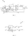
FIG. 1 illustrates an exemplary embodiment of an improved Dohertypower amplifier 100 for millimeter (MM) wave applications. Theamplifier 100 is suitable for use in a wireless handset or other portable device and also for use in a base station or any other wireless communication apparatus. - The
amplifier 100 comprises apower splitter 102 that receives a MM wave input signal (PIN). In an embodiment that is not covered by the claimed invention, apower detector 104 detects power on the input and provides adetection signal 106 to acontroller 108. A first output (split signal) 110 of thesplitter 102 is input to the "A" input of ahybrid plus coupler 112. A second output (split signal) 114 of thesplitter 102 is input to aphase shifter 116. The phase shiftedoutput signal 132 of thephase shifter 116 is a phase shifted version of thesecond split signal 114 and is input to the "C" input of thehybrid plus coupler 112. Both outputs of thesplitter 102 have power levels that are 3dB less than the input signal (PIN) power level. - In an embodiment, the
hybrid plus coupler 112 comprises a ¼wavelength extension 118. This extension is used to provide a 90 degree phase shift. Theextension 118 can be constructed by distributed elements, like transmission lines, or using lumped elements, like LC filters. In another embodiment that is not covered by the claimed invention, thehybrid plus coupler 108 comprise a 180 degree ring coupler as discussed below. - The
hybrid plus coupler 112 has a first output at terminal "B" coupled to a main power amplifier (PA1) 120 and a second output at terminal "D" coupled to an auxiliary power amplifier (PA2) 122. The output of thefirst power amplifier 120 is input to a (¼ wavelength phase shifter) 124 that is used to equalize the total phase shift from PIN to POUT between the PA1 signal path and the PA2 signal path. The output of thephase shifter 124 andsecond power amplifier 122 are coupled together to produce the output power signal (POUT). - During operation, the
hybrid plus coupler 112 generates first and second combinations of the phase shiftedversion signal 132 and the millimeter wavesecond signal 110. For example, the combinations of the input signals are provided at first and second output terminals (B and D), respectively. The first and second combinations set output power levels at the first and second output terminals, which in effect, distributes the input power on the hybrid coupler input terminals to its output terminals based on the phase shift introduced by thephase shifter 116. - In an embodiment that is not covered by the claimed invention, the
controller 108 outputs aphase control signal 126 to control the amount of phase shift applied by thephase shifter 116 based on thepower detection signal 106 detected by thepower detector 104. Thus, at low power, thecontroller 108 controls thephase shifter 116 to generate a phase shift such that the hybrid plus coupler 112 directs power to themain power amplifier 120 and away from theauxiliary power amplifier 122, thereby providing improved efficiency over conventional systems. In an embodiment, apower detector 128 is coupled to detect the power level of the output signal (POUT) and provide a detectedpower signal 130 to thecontroller 108. Thecontroller 108 operates to control the phase shift provided by thephase shifter 116 based on the detectedpower signal 130. Theextension 118 assists in distributing the power based on the phase shift introduced by thephase shifter 116. - Accordingly, an improved Doherty amplifier is provided that comprises a
hybrid plus coupler 112 to steer the input power distribution with thephase shifter 116 and therefore provide greater efficiency at low power. -
FIG. 2 shows an exemplary embodiment of ahybrid plus coupler 200. For example, thehybrid plus coupler 200 is suitable for use as thehybrid plus coupler 108 shown inFIG. 1 . Thehybrid plus coupler 200 comprises input terminals A and C and output terminals B and D. Thehybrid plus coupler 200 also comprisesextension 202 which is used to provide a 90 degree phase shift. Theextension 202 can be constructed by distributed elements, like transmission lines, or using lumped elements, like LC filters. A phase difference between the signals on the input terminals (A and C) results in the input power being redistributed on the output terminals (B and D). For example, assuming a and b are constant coefficients and the signals input to the A and C input terminals are:


- Therefore, if (a = b), then the follow power distributions result based on the phase difference between the input signals.
- If ϕ=90° then, B=0,

- If ϕ=-90° then, D=0,

- If ϕ = 0° then both amplifiers will be on with equal power
-
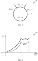
FIG. 3 shows an exemplary embodiment of ahybrid ring coupler 300, which is not covered by the claimed invention. For example, thehybrid ring coupler 300 is suitable for use as the hybrid pluscoupler 108 shown inFIG. 1 . Thehybrid ring coupler 300 comprises inputs A and C and outputs B and D. A phase difference between the signals at the input terminals (A and C) results in power being redistributed on the output terminals (B and D). For example, assuming the signals input to the A and C terminals are:


- Therefore, if (a = b), then the follow power distributions result based on the phase difference between the input signals.
- If ϕ = 0° then, B=0,

- If ϕ = 180° then, D=0,

- If ϕ = 90° then both amplifiers will be on with equal power
-
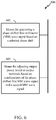
FIG. 4 shows anexemplary graph 400 that illustrates the increase in efficiency provided by exemplary embodiments of theimproved Doherty amplifier 100. For example, thegraph 400 includesplot line 402 representing the efficiency of a typical Doherty amplifier. Theplot line 404 represents the power amplifier efficiency (PAE) of an improved Doherty amplifier constructed in accordance with the disclosed embodiments where:
-
FIG. 5 shows anexemplary method 500 for providing an improved Doherty amplifier. For example, themethod 500 is performed by theamplifier 100 shown inFIG. 1 . - At
block 502, a MM wave signal to be amplified is input to a power splitter to generate first and second split signals. For example, the signal is input to thepower splitter 102 shown inFIG. 1 to generate thefirst split signal 110 and thesecond split signal 114. - At
block 504, the second split signal is phase shifted to generate a phase shifted split signal. For example, thesplit signal 114 is input into thephase shifter 116 to generate the phase shiftedsignal 132. - At
block 506, first and second combinations of the phase shifted version of the first signal and a millimeter wave second signal are generated at first and second output terminals, respectively. The first and second combinations set output power levels at the first and second output terminals. For example, the first split signal and the phase shifted split signal are input to the hybrid pluscoupler 112. For example, thesignal 110 and thesignal 132 are input to the input terminals (A and C) of the hybrid pluscoupler 112. The hybrid pluscoupler 112 hasextension 118 to provide a 90 degree phase shift as described above. The hybrid plus coupler operates to generate combinations of its input signals according to the equations shown above. Thus the hybrid plus coupler operates to adjust output power levels at its output terminals based on combinations of a phase shifted first MM wave signal and a second MM wave signal. - At
block 508, a power level is detected. For example, in an embodiment that is not part of the claimed invention thepower detector 104 detects the power of the input signal and provides thepower detection signal 106 to thecontroller 108. In another embodiment, thepower detector 128 detects the power of the output signal (POUT) and provides thepower detection signal 130 to thecontroller 108. - At
block 510, a phase shift is adjusted based on the detected power to improve efficiency. For example, thecontroller 108 outputs thephase control signal 126 to control the phase shift introduced by thephase shifter 116 so that the power distribution provided by the hybrid pluscoupler 112 provides improved efficiency over conventional systems. - Therefore the
method 500 operates to provide an improved Doherty amplifier using thephase shifter 116 and hybrid pluscoupler 112 to adjust the power distribution of the output to achieve improved efficiency. In other exemplary embodiments, the operations of themethod 500 may be rearranged or modified to provide the functions described herein. -
FIG. 6 shows an exemplary embodiment of aDoherty amplifier apparatus 600 that provides improved efficiency. For example, theapparatus 600 is suitable for use as theamplifier 100 shown inFIG. 1 . In an aspect, theapparatus 600 is implemented by one or more modules configured to provide the functions as described herein. For example, in an aspect, each module comprises hardware and/or hardware executing software. - The
apparatus 600 comprises a first module comprising means (602) for generating a phase shifted first millimeter (MM) wave signal based on a selected phase shift, which in an aspect comprisesphase shifter 116. - The
apparatus 600 also comprises a second module comprising means (604) for adjusting output power levels at output terminals based on combinations of the phase shifted first MM wave signal and a second MM wave signal, which in an aspect comprises the hybrid pluscoupler 112. - Those of skill in the art would understand that information and signals may be represented or processed using any of a variety of different technologies and techniques. For example, data, instructions, commands, information, signals, bits, symbols, and chips that may be referenced throughout the above description may be represented by voltages, currents, electromagnetic waves, magnetic fields or particles, optical fields or particles, or any combination thereof. It is further noted that transistor types and technologies may be substituted, rearranged or otherwise modified to achieve the same results. For example, circuits shown utilizing PMOS transistors may be modified to use NMOS transistors and vice versa. Thus, the amplifiers disclosed herein may be realized using a variety of transistor types and technologies and are not limited to those transistor types and technologies illustrated in the Drawings. For example, transistors types such as BJT, GaAs, MOSFET or any other transistor technology may be used.
- Those of skill would further appreciate that the various illustrative logical blocks, modules, circuits, and algorithm steps described in connection with the embodiments disclosed herein may be implemented as electronic hardware, computer software, or combinations of both. To clearly illustrate this interchangeability of hardware and software, various illustrative components, blocks, modules, circuits, and steps have been described above generally in terms of their functionality. Whether such functionality is implemented as hardware or software depends upon the particular application and design constraints imposed on the overall system. Skilled artisans may implement the described functionality in varying ways for each particular application, but such implementation decisions should not be interpreted as causing a departure from the scope of the exemplary embodiments of the invention.
- The various illustrative logical blocks, modules, and circuits described in connection with the embodiments disclosed herein may be implemented or performed with a general purpose processor, a Digital Signal Processor (DSP), an Application Specific Integrated Circuit (ASIC), a Field Programmable Gate Array (FPGA) or other programmable logic device, discrete gate or transistor logic, discrete hardware components, or any combination thereof designed to perform the functions described herein. A general purpose processor may be a microprocessor, but in the alternative, the processor may be any conventional processor, controller, microcontroller, or state machine. A processor may also be implemented as a combination of computing devices, e.g., a combination of a DSP and a microprocessor, a plurality of microprocessors, one or more microprocessors in conjunction with a DSP core, or any other such configuration.
- The steps of a method or algorithm described in connection with the embodiments disclosed herein may be embodied directly in hardware, in a software module executed by a processor, or in a combination of the two. A software module may reside in Random Access Memory (RAM), flash memory, Read Only Memory (ROM), Electrically Programmable ROM (EPROM), Electrically Erasable Programmable ROM (EEPROM), registers, hard disk, a removable disk, a CD-ROM, or any other form of storage medium known in the art. An exemplary storage medium is coupled to the processor such that the processor can read information from, and write information to, the storage medium. In the alternative, the storage medium may be integral to the processor. The processor and the storage medium may reside in an ASIC. The ASIC may reside in a user terminal. In the alternative, the processor and the storage medium may reside as discrete components in a user terminal.
- In one or more exemplary embodiments, the functions described may be implemented in hardware, software, firmware, or any combination thereof. If implemented in software, the functions may be stored on or transmitted over as one or more instructions or code on a computer-readable medium. Computer-readable media includes both non-transitory computer storage media and communication media including any medium that facilitates transfer of a computer program from one place to another. A non-transitory storage media may be any available media that can be accessed by a computer. By way of example, and not limitation, such computer-readable media can comprise RAM, ROM, EEPROM, CD-ROM or other optical disk storage, magnetic disk storage or other magnetic storage devices, or any other medium that can be used to carry or store desired program code in the form of instructions or data structures and that can be accessed by a computer. Also, any connection is properly termed a computer-readable medium. For example, if the software is transmitted from a website, server, or other remote source using a coaxial cable, fiber optic cable, twisted pair, digital subscriber line (DSL), or wireless technologies such as infrared, radio, and microwave, then the coaxial cable, fiber optic cable, twisted pair, DSL, or wireless technologies such as infrared, radio, and microwave are included in the definition of medium. Disk and disc, as used herein, includes compact disc (CD), laser disc, optical disc, digital versatile disc (DVD), floppy disk and blu-ray disc where disks usually reproduce data magnetically, while discs reproduce data optically with lasers. Combinations of the above should also be included within the scope of computer-readable media.
- The description of the disclosed exemplary embodiments is provided to enable any person skilled in the art to make or use the invention. Various modifications to these exemplary embodiments will be readily apparent to those skilled in the art, and the generic principles defined herein may be applied to other embodiments without departing from the scope of the invention.
Claims (10)
- A method for power amplification in an apparatus, comprising:splitting (502) a millimeter, MM, wave input signal to generate a first MM wave signal and a second MM wave signalgenerating a phase shifted first MM wave signal based on a selected phase shift (504) and the first MM wave signal;providing intermediate output power levels at first and second output terminals (B, D) of a hybrid coupler based on combinations of the phase shifted first MM wave signal and the second MM wave signal (506), wherein the hybrid coupler comprises a 1/4 wavelength extension (118) providing a 90 degree phase shift at the second output terminal (D) of the hybrid coupler, and
wherein the first output terminal (B) of the hybrid coupler is coupled to an input of a first power amplifier (PA1), and the second output terminal (D) of the hybrid coupler is coupled to an input of a second power amplifier (PA2); andadjusting the intermediate output power levels by adjusting the selected phase shift, wherein the selected phase shift is adjusted based on a detected output power level of the apparatus (508, 510). - The method of claim 1, comprising:providing intermediate output power at the first output terminal (B) based on a first combination; andproviding intermediate output power at the second output terminal (D) based on a second combination.
- The method of claim 1, wherein the first MM wave signal and the second MM wave signal are at substantially equal power levels (502).
- The method of claim 1, further comprising generating a power distribution between the first output terminal (B) and the second output terminal (D) based on a phase difference (ϕ) between the second MM wave signal and the phase shifted first MM wave signal, wherein the power distribution between the first and second output terminals (B, D) is determined from:


- An apparatus for power amplification comprising:means for splitting (102) a millimeter, MM, wave input signal to generate a first MM wave signal and a second MM wave signalmeans for generating (116) a phase shifted first MM wave signal (132) based on a selected phase shift and the first MM wave signal;means for providing (112) intermediate output power levels at first and second output terminals (B, D) of said means for providing based on combinations of the phase shifted first MM wave signal (132) and the second MM wave signal (110), wherein the means for providing (112) are a hybrid coupler comprising a 1/4 wavelength extension (118) configured to provide a 90 degree phase shift at the second output terminal (D) of the hybrid coupler, and wherein the first output terminal (B) of the hybrid coupler is coupled to an input of a first power amplifier (PA1), and the second output terminal (D) of the hybrid coupler is coupled to an input of a second power amplifier (PA2); andmeans for adjusting the intermediate output power levels by adjusting the selected phase shift comprising means for adjusting the selected phase shift (108) based on a detected output power level (130) of the apparatus.
- The apparatus of claim 5, further comprising:means for providing intermediate output power at the first output terminal (B) based on a first combination; andmeans for providing intermediate output power at the second output terminal (D) based on a second combination.
- The apparatus of claim 5, further comprising means for generating a power distribution between the afirst output terminal (B) and the second output terminal (D) based on a phase difference (ϕ) between the second MM wave signal and the phase shifted first MM wave signal, wherein the power distribution between the first and second output terminals (B, D) is determined from:


- The apparatus of claim 5, wherein the apparatus further comprises means to amplify a MM wave input signal in at least one of a wireless device and a base station.
- The apparatus of claim 5, wherein the apparatus is configured as a Doherty amplifier.
- The apparatus of claim 5, the means for splitting comprising a splitter configured to receive a MM wave input signal (P_IN) and to generate the first MM wave signal (114) and the second MM wave signal (110) at substantially equal power levels, the first MM wave signal is input to the means for generating the phase shifted first MM wave signal (116).
Applications Claiming Priority (2)
| Application Number | Priority Date | Filing Date | Title |
|---|---|---|---|
| US13/424,199 US8970297B2 (en) | 2012-03-19 | 2012-03-19 | Reconfigurable input power distribution doherty amplifier with improved efficiency |
| PCT/US2013/033022 WO2013142529A2 (en) | 2012-03-19 | 2013-03-19 | Reconfigurable input power distribution doherty amplifier with improved efficiency |
Publications (2)
| Publication Number | Publication Date |
|---|---|
| EP2828970A2 EP2828970A2 (en) | 2015-01-28 |
| EP2828970B1 true EP2828970B1 (en) | 2021-03-10 |
Family
ID=48048259
Family Applications (1)
| Application Number | Title | Priority Date | Filing Date |
|---|---|---|---|
| EP13714459.8A Active EP2828970B1 (en) | 2012-03-19 | 2013-03-19 | Reconfigurable input power distribution doherty amplifier with improved efficiency |
Country Status (6)
| Country | Link |
|---|---|
| US (1) | US8970297B2 (en) |
| EP (1) | EP2828970B1 (en) |
| JP (1) | JP6185551B2 (en) |
| KR (1) | KR20140146121A (en) |
| CN (1) | CN104205625B (en) |
| WO (1) | WO2013142529A2 (en) |
Families Citing this family (18)
| Publication number | Priority date | Publication date | Assignee | Title |
|---|---|---|---|---|
| US9306502B2 (en) | 2011-05-09 | 2016-04-05 | Qualcomm Incorporated | System providing switchable impedance transformer matching for power amplifiers |
| US9203348B2 (en) | 2012-01-27 | 2015-12-01 | Freescale Semiconductor, Inc. | Adjustable power splitters and corresponding methods and apparatus |
| US8514007B1 (en) | 2012-01-27 | 2013-08-20 | Freescale Semiconductor, Inc. | Adjustable power splitter and corresponding methods and apparatus |
| US9431969B2 (en) * | 2012-12-11 | 2016-08-30 | Rf Micro Devices, Inc. | Doherty power amplifier with tunable impedance load |
| US9031518B2 (en) | 2012-12-17 | 2015-05-12 | Qualcomm Incorporated | Concurrent hybrid matching network |
| US9397617B2 (en) | 2013-06-25 | 2016-07-19 | Rf Micro Devices, Inc. | Multi-broadband Doherty power amplifier |
| US9948243B2 (en) | 2013-09-30 | 2018-04-17 | Qorvo Us, Inc. | Reconfigurable load modulation amplifier |
| US9484865B2 (en) | 2013-09-30 | 2016-11-01 | Qorvo Us, Inc. | Reconfigurable load modulation amplifier |
| US9225291B2 (en) * | 2013-10-29 | 2015-12-29 | Freescale Semiconductor, Inc. | Adaptive adjustment of power splitter |
| US9369095B2 (en) | 2014-01-27 | 2016-06-14 | Rf Micro Devices, Inc. | Unbalanced linear power amplifier |
| US9774299B2 (en) | 2014-09-29 | 2017-09-26 | Nxp Usa, Inc. | Modifiable signal adjustment devices for power amplifiers and corresponding methods and apparatus |
| US9831837B2 (en) | 2014-11-05 | 2017-11-28 | Qualcomm Incorporated | Dynamic power divider circuits and methods |
| US9647611B1 (en) | 2015-10-28 | 2017-05-09 | Nxp Usa, Inc. | Reconfigurable power splitters and amplifiers, and corresponding methods |
| CN107147366B (en) * | 2017-06-12 | 2023-08-29 | 广州慧智微电子股份有限公司 | Temperature compensation circuit of radio frequency power amplifier |
| KR102463954B1 (en) * | 2018-01-22 | 2022-11-04 | 미쓰비시덴키 가부시키가이샤 | amplifier |
| CN109167580B (en) * | 2018-10-30 | 2022-06-14 | 北京振兴计量测试研究所 | Planar four-path power synthesis amplifier |
| GB201817747D0 (en) * | 2018-10-31 | 2018-12-19 | Leonardo Mw Ltd | A radio frequency power amplifier |
| FR3115113B1 (en) * | 2020-10-09 | 2023-01-06 | St Microelectronics Sa | Method and device for determining the phase difference between two signals, in particular radiofrequency signals |
Citations (3)
| Publication number | Priority date | Publication date | Assignee | Title |
|---|---|---|---|---|
| JPS53136945A (en) * | 1977-05-06 | 1978-11-29 | Fujitsu Ltd | Parallel-operation amplifier |
| JP2010273212A (en) * | 2009-05-22 | 2010-12-02 | Sumitomo Electric Ind Ltd | Amplification apparatus and radio base station |
| WO2011060706A1 (en) * | 2009-11-18 | 2011-05-26 | 中兴通讯股份有限公司 | Implementation method for power amplification circuit and power amplification apparatus |
Family Cites Families (62)
| Publication number | Priority date | Publication date | Assignee | Title |
|---|---|---|---|---|
| US4490684A (en) * | 1983-01-03 | 1984-12-25 | Motorola, Inc. | Adaptive quadrature combining apparatus |
| JPS61265910A (en) * | 1985-05-20 | 1986-11-25 | Fujitsu Ltd | High power amplifier |
| US5287069A (en) * | 1990-02-07 | 1994-02-15 | Fujitsu Limited | Constant-amplitude wave combination type amplifier |
| JPH04288703A (en) * | 1991-02-01 | 1992-10-13 | Fujitsu Ltd | Rat race with built-in absorption resistor and amplifier |
| JPH06120750A (en) * | 1992-10-01 | 1994-04-28 | Nec Corp | Power amplifier |
| JP2001203540A (en) * | 2000-01-19 | 2001-07-27 | Hitachi Ltd | High frequency power amplifier |
| SE520760C2 (en) | 2000-06-06 | 2003-08-19 | Ericsson Telefon Ab L M | Doherty multistage amplifier |
| US6639463B1 (en) * | 2000-08-24 | 2003-10-28 | Lucent Technologies Inc. | Adaptive power amplifier system and method |
| US6384679B1 (en) | 2000-11-15 | 2002-05-07 | National Semiconductor Corporation | Rail-to-rail amplifier with reduced GM and compensating cap |
| US6472934B1 (en) * | 2000-12-29 | 2002-10-29 | Ericsson Inc. | Triple class E Doherty amplifier topology for high efficiency signal transmitters |
| JP3809777B2 (en) | 2001-05-30 | 2006-08-16 | ソニー株式会社 | Power amplifier |
| US6522160B1 (en) | 2001-06-13 | 2003-02-18 | Micron Technology, Inc. | Input buffer with automatic switching point adjustment circuitry, and synchronous DRAM device including same |
| JP3947373B2 (en) | 2001-07-31 | 2007-07-18 | 株式会社ルネサステクノロジ | High frequency power amplifier |
| US6806767B2 (en) | 2002-07-09 | 2004-10-19 | Anadigics, Inc. | Power amplifier with load switching circuit |
| KR100450744B1 (en) | 2002-08-29 | 2004-10-01 | 학교법인 포항공과대학교 | Doherty amplifier |
| US6794935B2 (en) | 2002-10-17 | 2004-09-21 | Motorola Inc. | Power amplification circuit and method for supplying power at a plurality of desired power output levels |
| JP2004221646A (en) | 2003-01-09 | 2004-08-05 | Nec Corp | Doherty amplifier |
| DE10308848A1 (en) | 2003-02-27 | 2004-09-09 | Marconi Communications Gmbh | Integrated amplifier arrangement |
| JP3907052B2 (en) | 2003-03-07 | 2007-04-18 | ソニー・エリクソン・モバイルコミュニケーションズ株式会社 | Communication terminal device and amplifier circuit |
| US6922102B2 (en) * | 2003-03-28 | 2005-07-26 | Andrew Corporation | High efficiency amplifier |
| US7444124B1 (en) | 2003-05-14 | 2008-10-28 | Marvell International Ltd. | Adjustable segmented power amplifier |
| TW200518345A (en) | 2003-08-08 | 2005-06-01 | Renesas Tech Corp | Semiconductor device |
| US20050134377A1 (en) | 2003-12-23 | 2005-06-23 | Dent Paul W. | Doherty amplifier |
| US7157965B1 (en) | 2004-06-21 | 2007-01-02 | Qualcomm Incorporated | Summing power amplifier |
| CN100542011C (en) | 2004-06-29 | 2009-09-16 | Nxp股份有限公司 | Integrated doherty type amplifier installation with high effect |
| JP4715994B2 (en) | 2004-08-26 | 2011-07-06 | 日本電気株式会社 | Doherty amplifier parallel operation circuit |
| US20060105733A1 (en) | 2004-11-16 | 2006-05-18 | Singh Donald R | System and method for developing ultra-sensitive microwave and millimeter wave phase discriminators |
| US7295065B2 (en) | 2004-11-18 | 2007-11-13 | Beecem Communications Inc. | High efficiency doherty amplifier with a segmented main amplifier |
| CN101091322B (en) | 2004-12-24 | 2010-04-28 | 华为技术有限公司 | Quasi-linear high power amplifier and method for amplifying radio frequency signal |
| EP1886404A2 (en) | 2005-05-20 | 2008-02-13 | Nxp B.V. | Integrated doherty type amplifier arrangement with high power efficiency |
| US7183843B1 (en) * | 2005-06-27 | 2007-02-27 | Rockwell Collins, Inc. | Electronically tuned power amplifier |
| KR100752280B1 (en) | 2005-12-14 | 2007-08-28 | 삼성전자주식회사 | Device for matching frequency of antenna automatically in wireless terminal |
| DE102006008790A1 (en) * | 2006-02-24 | 2007-09-06 | Infineon Technologies Ag | Modulation device for a transmission path, method for signal processing in a transmission path and transmission path with the modulation device |
| US7719141B2 (en) | 2006-11-16 | 2010-05-18 | Star Rf, Inc. | Electronic switch network |
| JP4985654B2 (en) | 2006-11-21 | 2012-07-25 | 日本電気株式会社 | RF circuit |
| US7561854B2 (en) | 2006-12-01 | 2009-07-14 | Harris Corporation | Lossless transmit path antenna switch circuit |
| KR100814415B1 (en) | 2007-02-14 | 2008-03-18 | 포항공과대학교 산학협력단 | Highly efficient doherty amplifier using a harmonic control circuit |
| US20080207256A1 (en) | 2007-02-22 | 2008-08-28 | Texas Instruments Incorporated | Concurrent impedance matching of a wireless transceiver |
| EP2145385B1 (en) * | 2007-04-23 | 2018-10-17 | Dali Systems Co. Ltd | N-way doherty distributed power amplifier |
| CN101803181A (en) | 2007-09-03 | 2010-08-11 | Nxp股份有限公司 | multi-way doherty amplifier |
| US7609115B2 (en) | 2007-09-07 | 2009-10-27 | Raytheon Company | Input circuitry for transistor power amplifier and method for designing such circuitry |
| KR20090071834A (en) | 2007-12-28 | 2009-07-02 | 성균관대학교산학협력단 | Harmonic turned doherty amplifier |
| KR101547818B1 (en) | 2008-01-29 | 2015-08-27 | 삼성전자주식회사 | Apparatus for transmit/receive switch in tdd wireless communication system |
| US8103221B2 (en) | 2008-05-30 | 2012-01-24 | National Ict Australia Limited | High-isolation transmit/receive switch on CMOS for millimeter-wave applications |
| JP2009303040A (en) | 2008-06-16 | 2009-12-24 | Toshiba Corp | High-frequency power amplifier and amplification method |
| US9300508B2 (en) | 2008-08-07 | 2016-03-29 | Trex Enterprises Corp. | High data rate milllimeter wave radio on a chip |
| US7952433B2 (en) | 2008-11-25 | 2011-05-31 | Samsung Electro-Mechanics Company | Power amplifiers with discrete power control |
| US7863979B2 (en) | 2009-01-26 | 2011-01-04 | Skyworks Solutions, Inc. | High efficiency power amplifier having embedded switching |
| US8666340B2 (en) | 2009-03-03 | 2014-03-04 | Broadcom Corporation | Method and system for on-chip impedance control to impedance match a configurable front end |
| JP5163577B2 (en) | 2009-03-27 | 2013-03-13 | 富士通株式会社 | Amplifier circuit and transceiver |
| US8432237B2 (en) | 2009-05-21 | 2013-04-30 | Qualcomm, Incorporated | Output circuit with integrated impedance matching, power combining and filtering for power amplifiers and other circuits |
| KR101573719B1 (en) | 2009-07-31 | 2015-12-02 | 삼성전자주식회사 | Apparatus and method for protecting receive circuits in tdd wireless communication system |
| US8295212B2 (en) | 2009-08-05 | 2012-10-23 | Alcatel Lucent | System and method for TDD/TMA with hybrid bypass switch of receiving amplifier |
| US9064627B2 (en) | 2009-10-12 | 2015-06-23 | St-Ericsson Sa | Integrated transformer with multiple transformation ratios |
| JP5705122B2 (en) | 2009-10-23 | 2015-04-22 | 日本碍子株式会社 | Doherty amplifier synthesizer |
| EP2339745A1 (en) | 2009-12-15 | 2011-06-29 | Nxp B.V. | Doherty amplifier |
| US9048787B2 (en) | 2010-04-20 | 2015-06-02 | Rf Micro Devices, Inc. | Combined RF detector and RF attenuator with concurrent outputs |
| US8626084B2 (en) | 2010-05-13 | 2014-01-07 | Qualcomm, Incorporated | Area efficient concurrent matching transceiver |
| US8760240B2 (en) | 2010-09-15 | 2014-06-24 | Wilocity, Ltd. | Method for designing coupling-function based millimeter wave electrical elements |
| US8611834B2 (en) | 2010-11-01 | 2013-12-17 | Cree, Inc. | Matching network for transmission circuitry |
| US9306502B2 (en) | 2011-05-09 | 2016-04-05 | Qualcomm Incorporated | System providing switchable impedance transformer matching for power amplifiers |
| US9031518B2 (en) | 2012-12-17 | 2015-05-12 | Qualcomm Incorporated | Concurrent hybrid matching network |
-
2012
- 2012-03-19 US US13/424,199 patent/US8970297B2/en active Active
-
2013
- 2013-03-19 KR KR1020147029063A patent/KR20140146121A/en not_active Application Discontinuation
- 2013-03-19 EP EP13714459.8A patent/EP2828970B1/en active Active
- 2013-03-19 JP JP2015501863A patent/JP6185551B2/en not_active Expired - Fee Related
- 2013-03-19 WO PCT/US2013/033022 patent/WO2013142529A2/en active Application Filing
- 2013-03-19 CN CN201380014736.8A patent/CN104205625B/en active Active
Patent Citations (3)
| Publication number | Priority date | Publication date | Assignee | Title |
|---|---|---|---|---|
| JPS53136945A (en) * | 1977-05-06 | 1978-11-29 | Fujitsu Ltd | Parallel-operation amplifier |
| JP2010273212A (en) * | 2009-05-22 | 2010-12-02 | Sumitomo Electric Ind Ltd | Amplification apparatus and radio base station |
| WO2011060706A1 (en) * | 2009-11-18 | 2011-05-26 | 中兴通讯股份有限公司 | Implementation method for power amplification circuit and power amplification apparatus |
Also Published As
| Publication number | Publication date |
|---|---|
| CN104205625A (en) | 2014-12-10 |
| KR20140146121A (en) | 2014-12-24 |
| JP2015514360A (en) | 2015-05-18 |
| CN104205625B (en) | 2017-06-20 |
| EP2828970A2 (en) | 2015-01-28 |
| WO2013142529A3 (en) | 2013-11-14 |
| WO2013142529A2 (en) | 2013-09-26 |
| US8970297B2 (en) | 2015-03-03 |
| JP6185551B2 (en) | 2017-08-23 |
| US20130241640A1 (en) | 2013-09-19 |
Similar Documents
| Publication | Publication Date | Title |
|---|---|---|
| EP2828970B1 (en) | Reconfigurable input power distribution doherty amplifier with improved efficiency | |
| CN102197584B (en) | Power amplifier and amplifying method employed therein | |
| KR101126054B1 (en) | Quadrature output low noise transconductance amplifier having differential input | |
| US8774742B2 (en) | High efficiency transmitter | |
| US7994859B2 (en) | High-speed, multi-stage class AB amplifiers | |
| EP3058654B1 (en) | Power amplifier for amplification of an input signal into an output signal | |
| EP2451074B1 (en) | Amplifier | |
| JP4754019B2 (en) | MIMO transmitter | |
| US20100289571A1 (en) | Apparatus and method for maximizing performance of peaking amplifier in doherty amplifier | |
| EP2430749B1 (en) | Switchable input pair operational amplifiers | |
| JP2016063543A (en) | Amplifier with base current reuse | |
| EP2634916A1 (en) | Doherty amplifier | |
| EP2538548B1 (en) | Method and device for controlling peak amplifier, and doherty power amplifier | |
| JP5331732B2 (en) | Envelope tracking power amplifier and envelope tracking amplification method | |
| US8952754B2 (en) | Linearization of heterogeneous power amplifier systems | |
| JP2011211655A (en) | High frequency amplifier | |
| US20150054581A1 (en) | Combination nmos/pmos power amplifier | |
| CN105684317A (en) | Apparatus and method for controlling signal gain in wireless transmitter | |
| US9106198B2 (en) | High power tunable capacitor | |
| CN112564647B (en) | Power amplifier, power amplification method and storage medium | |
| KR101500570B1 (en) | Asymmetric Doherty Amplifier | |
| WO2015131385A1 (en) | Method and apparatus for modulating power supply | |
| KR20120029015A (en) | Hybrid vehicle's audio system and amplifying method of their audio signal | |
| JP2010068283A (en) | Transmitter | |
| JP2009111887A (en) | Am transmitter and modulation method for the same |
Legal Events
| Date | Code | Title | Description |
|---|---|---|---|
| PUAI | Public reference made under article 153(3) epc to a published international application that has entered the european phase |
Free format text: ORIGINAL CODE: 0009012 |
|
| 17P | Request for examination filed |
Effective date: 20141014 |
|
| AK | Designated contracting states |
Kind code of ref document: A2 Designated state(s): AL AT BE BG CH CY CZ DE DK EE ES FI FR GB GR HR HU IE IS IT LI LT LU LV MC MK MT NL NO PL PT RO RS SE SI SK SM TR |
|
| AX | Request for extension of the european patent |
Extension state: BA ME |
|
| DAX | Request for extension of the european patent (deleted) | ||
| STAA | Information on the status of an ep patent application or granted ep patent |
Free format text: STATUS: EXAMINATION IS IN PROGRESS |
|
| 17Q | First examination report despatched |
Effective date: 20181219 |
|
| GRAP | Despatch of communication of intention to grant a patent |
Free format text: ORIGINAL CODE: EPIDOSNIGR1 |
|
| STAA | Information on the status of an ep patent application or granted ep patent |
Free format text: STATUS: GRANT OF PATENT IS INTENDED |
|
| RIC1 | Information provided on ipc code assigned before grant |
Ipc: H03F 3/189 20060101ALI20200915BHEP Ipc: H03F 1/02 20060101AFI20200915BHEP |
|
| INTG | Intention to grant announced |
Effective date: 20201006 |
|
| GRAS | Grant fee paid |
Free format text: ORIGINAL CODE: EPIDOSNIGR3 |
|
| GRAA | (expected) grant |
Free format text: ORIGINAL CODE: 0009210 |
|
| STAA | Information on the status of an ep patent application or granted ep patent |
Free format text: STATUS: THE PATENT HAS BEEN GRANTED |
|
| AK | Designated contracting states |
Kind code of ref document: B1 Designated state(s): AL AT BE BG CH CY CZ DE DK EE ES FI FR GB GR HR HU IE IS IT LI LT LU LV MC MK MT NL NO PL PT RO RS SE SI SK SM TR |
|
| REG | Reference to a national code |
Ref country code: GB Ref legal event code: FG4D |
|
| REG | Reference to a national code |
Ref country code: AT Ref legal event code: REF Ref document number: 1370950 Country of ref document: AT Kind code of ref document: T Effective date: 20210315 Ref country code: CH Ref legal event code: EP |
|
| REG | Reference to a national code |
Ref country code: IE Ref legal event code: FG4D |
|
| REG | Reference to a national code |
Ref country code: DE Ref legal event code: R096 Ref document number: 602013076162 Country of ref document: DE |
|
| PGFP | Annual fee paid to national office [announced via postgrant information from national office to epo] |
Ref country code: FR Payment date: 20210310 Year of fee payment: 9 |
|
| PGFP | Annual fee paid to national office [announced via postgrant information from national office to epo] |
Ref country code: DE Payment date: 20210219 Year of fee payment: 9 Ref country code: GB Payment date: 20210310 Year of fee payment: 9 |
|
| REG | Reference to a national code |
Ref country code: LT Ref legal event code: MG9D |
|
| PG25 | Lapsed in a contracting state [announced via postgrant information from national office to epo] |
Ref country code: HR Free format text: LAPSE BECAUSE OF FAILURE TO SUBMIT A TRANSLATION OF THE DESCRIPTION OR TO PAY THE FEE WITHIN THE PRESCRIBED TIME-LIMIT Effective date: 20210310 Ref country code: GR Free format text: LAPSE BECAUSE OF FAILURE TO SUBMIT A TRANSLATION OF THE DESCRIPTION OR TO PAY THE FEE WITHIN THE PRESCRIBED TIME-LIMIT Effective date: 20210611 Ref country code: FI Free format text: LAPSE BECAUSE OF FAILURE TO SUBMIT A TRANSLATION OF THE DESCRIPTION OR TO PAY THE FEE WITHIN THE PRESCRIBED TIME-LIMIT Effective date: 20210310 Ref country code: LT Free format text: LAPSE BECAUSE OF FAILURE TO SUBMIT A TRANSLATION OF THE DESCRIPTION OR TO PAY THE FEE WITHIN THE PRESCRIBED TIME-LIMIT Effective date: 20210310 Ref country code: BG Free format text: LAPSE BECAUSE OF FAILURE TO SUBMIT A TRANSLATION OF THE DESCRIPTION OR TO PAY THE FEE WITHIN THE PRESCRIBED TIME-LIMIT Effective date: 20210610 Ref country code: NO Free format text: LAPSE BECAUSE OF FAILURE TO SUBMIT A TRANSLATION OF THE DESCRIPTION OR TO PAY THE FEE WITHIN THE PRESCRIBED TIME-LIMIT Effective date: 20210610 |
|
| REG | Reference to a national code |
Ref country code: AT Ref legal event code: MK05 Ref document number: 1370950 Country of ref document: AT Kind code of ref document: T Effective date: 20210310 |
|
| REG | Reference to a national code |
Ref country code: NL Ref legal event code: MP Effective date: 20210310 |
|
| PG25 | Lapsed in a contracting state [announced via postgrant information from national office to epo] |
Ref country code: SE Free format text: LAPSE BECAUSE OF FAILURE TO SUBMIT A TRANSLATION OF THE DESCRIPTION OR TO PAY THE FEE WITHIN THE PRESCRIBED TIME-LIMIT Effective date: 20210310 Ref country code: RS Free format text: LAPSE BECAUSE OF FAILURE TO SUBMIT A TRANSLATION OF THE DESCRIPTION OR TO PAY THE FEE WITHIN THE PRESCRIBED TIME-LIMIT Effective date: 20210310 Ref country code: LV Free format text: LAPSE BECAUSE OF FAILURE TO SUBMIT A TRANSLATION OF THE DESCRIPTION OR TO PAY THE FEE WITHIN THE PRESCRIBED TIME-LIMIT Effective date: 20210310 |
|
| PG25 | Lapsed in a contracting state [announced via postgrant information from national office to epo] |
Ref country code: NL Free format text: LAPSE BECAUSE OF FAILURE TO SUBMIT A TRANSLATION OF THE DESCRIPTION OR TO PAY THE FEE WITHIN THE PRESCRIBED TIME-LIMIT Effective date: 20210310 |
|
| PG25 | Lapsed in a contracting state [announced via postgrant information from national office to epo] |
Ref country code: SM Free format text: LAPSE BECAUSE OF FAILURE TO SUBMIT A TRANSLATION OF THE DESCRIPTION OR TO PAY THE FEE WITHIN THE PRESCRIBED TIME-LIMIT Effective date: 20210310 Ref country code: AT Free format text: LAPSE BECAUSE OF FAILURE TO SUBMIT A TRANSLATION OF THE DESCRIPTION OR TO PAY THE FEE WITHIN THE PRESCRIBED TIME-LIMIT Effective date: 20210310 Ref country code: CZ Free format text: LAPSE BECAUSE OF FAILURE TO SUBMIT A TRANSLATION OF THE DESCRIPTION OR TO PAY THE FEE WITHIN THE PRESCRIBED TIME-LIMIT Effective date: 20210310 Ref country code: EE Free format text: LAPSE BECAUSE OF FAILURE TO SUBMIT A TRANSLATION OF THE DESCRIPTION OR TO PAY THE FEE WITHIN THE PRESCRIBED TIME-LIMIT Effective date: 20210310 |
|
| REG | Reference to a national code |
Ref country code: CH Ref legal event code: PL |
|
| PG25 | Lapsed in a contracting state [announced via postgrant information from national office to epo] |
Ref country code: RO Free format text: LAPSE BECAUSE OF FAILURE TO SUBMIT A TRANSLATION OF THE DESCRIPTION OR TO PAY THE FEE WITHIN THE PRESCRIBED TIME-LIMIT Effective date: 20210310 Ref country code: IS Free format text: LAPSE BECAUSE OF FAILURE TO SUBMIT A TRANSLATION OF THE DESCRIPTION OR TO PAY THE FEE WITHIN THE PRESCRIBED TIME-LIMIT Effective date: 20210710 Ref country code: SK Free format text: LAPSE BECAUSE OF FAILURE TO SUBMIT A TRANSLATION OF THE DESCRIPTION OR TO PAY THE FEE WITHIN THE PRESCRIBED TIME-LIMIT Effective date: 20210310 Ref country code: ES Free format text: LAPSE BECAUSE OF FAILURE TO SUBMIT A TRANSLATION OF THE DESCRIPTION OR TO PAY THE FEE WITHIN THE PRESCRIBED TIME-LIMIT Effective date: 20210310 Ref country code: PT Free format text: LAPSE BECAUSE OF FAILURE TO SUBMIT A TRANSLATION OF THE DESCRIPTION OR TO PAY THE FEE WITHIN THE PRESCRIBED TIME-LIMIT Effective date: 20210712 Ref country code: PL Free format text: LAPSE BECAUSE OF FAILURE TO SUBMIT A TRANSLATION OF THE DESCRIPTION OR TO PAY THE FEE WITHIN THE PRESCRIBED TIME-LIMIT Effective date: 20210310 |
|
| REG | Reference to a national code |
Ref country code: DE Ref legal event code: R097 Ref document number: 602013076162 Country of ref document: DE |
|
| REG | Reference to a national code |
Ref country code: BE Ref legal event code: MM Effective date: 20210331 |
|
| PLBE | No opposition filed within time limit |
Free format text: ORIGINAL CODE: 0009261 |
|
| STAA | Information on the status of an ep patent application or granted ep patent |
Free format text: STATUS: NO OPPOSITION FILED WITHIN TIME LIMIT |
|
| PG25 | Lapsed in a contracting state [announced via postgrant information from national office to epo] |
Ref country code: MC Free format text: LAPSE BECAUSE OF FAILURE TO SUBMIT A TRANSLATION OF THE DESCRIPTION OR TO PAY THE FEE WITHIN THE PRESCRIBED TIME-LIMIT Effective date: 20210310 Ref country code: LU Free format text: LAPSE BECAUSE OF NON-PAYMENT OF DUE FEES Effective date: 20210319 Ref country code: LI Free format text: LAPSE BECAUSE OF NON-PAYMENT OF DUE FEES Effective date: 20210331 Ref country code: AL Free format text: LAPSE BECAUSE OF FAILURE TO SUBMIT A TRANSLATION OF THE DESCRIPTION OR TO PAY THE FEE WITHIN THE PRESCRIBED TIME-LIMIT Effective date: 20210310 Ref country code: CH Free format text: LAPSE BECAUSE OF NON-PAYMENT OF DUE FEES Effective date: 20210331 Ref country code: DK Free format text: LAPSE BECAUSE OF FAILURE TO SUBMIT A TRANSLATION OF THE DESCRIPTION OR TO PAY THE FEE WITHIN THE PRESCRIBED TIME-LIMIT Effective date: 20210310 Ref country code: IE Free format text: LAPSE BECAUSE OF NON-PAYMENT OF DUE FEES Effective date: 20210319 |
|
| 26N | No opposition filed |
Effective date: 20211213 |
|
| PG25 | Lapsed in a contracting state [announced via postgrant information from national office to epo] |
Ref country code: SI Free format text: LAPSE BECAUSE OF FAILURE TO SUBMIT A TRANSLATION OF THE DESCRIPTION OR TO PAY THE FEE WITHIN THE PRESCRIBED TIME-LIMIT Effective date: 20210310 |
|
| PG25 | Lapsed in a contracting state [announced via postgrant information from national office to epo] |
Ref country code: IT Free format text: LAPSE BECAUSE OF FAILURE TO SUBMIT A TRANSLATION OF THE DESCRIPTION OR TO PAY THE FEE WITHIN THE PRESCRIBED TIME-LIMIT Effective date: 20210310 |
|
| PG25 | Lapsed in a contracting state [announced via postgrant information from national office to epo] |
Ref country code: IS Free format text: LAPSE BECAUSE OF FAILURE TO SUBMIT A TRANSLATION OF THE DESCRIPTION OR TO PAY THE FEE WITHIN THE PRESCRIBED TIME-LIMIT Effective date: 20210710 |
|
| PG25 | Lapsed in a contracting state [announced via postgrant information from national office to epo] |
Ref country code: BE Free format text: LAPSE BECAUSE OF NON-PAYMENT OF DUE FEES Effective date: 20210331 |
|
| REG | Reference to a national code |
Ref country code: DE Ref legal event code: R119 Ref document number: 602013076162 Country of ref document: DE |
|
| GBPC | Gb: european patent ceased through non-payment of renewal fee |
Effective date: 20220319 |
|
| PG25 | Lapsed in a contracting state [announced via postgrant information from national office to epo] |
Ref country code: GB Free format text: LAPSE BECAUSE OF NON-PAYMENT OF DUE FEES Effective date: 20220319 Ref country code: FR Free format text: LAPSE BECAUSE OF NON-PAYMENT OF DUE FEES Effective date: 20220331 Ref country code: DE Free format text: LAPSE BECAUSE OF NON-PAYMENT OF DUE FEES Effective date: 20221001 |
|
| PG25 | Lapsed in a contracting state [announced via postgrant information from national office to epo] |
Ref country code: HU Free format text: LAPSE BECAUSE OF FAILURE TO SUBMIT A TRANSLATION OF THE DESCRIPTION OR TO PAY THE FEE WITHIN THE PRESCRIBED TIME-LIMIT; INVALID AB INITIO Effective date: 20130319 |
|
| PG25 | Lapsed in a contracting state [announced via postgrant information from national office to epo] |
Ref country code: CY Free format text: LAPSE BECAUSE OF FAILURE TO SUBMIT A TRANSLATION OF THE DESCRIPTION OR TO PAY THE FEE WITHIN THE PRESCRIBED TIME-LIMIT Effective date: 20210310 |