JP5705122B2 - Doherty amplifier synthesizer - Google Patents
Doherty amplifier synthesizer Download PDFInfo
- Publication number
- JP5705122B2 JP5705122B2 JP2011537180A JP2011537180A JP5705122B2 JP 5705122 B2 JP5705122 B2 JP 5705122B2 JP 2011537180 A JP2011537180 A JP 2011537180A JP 2011537180 A JP2011537180 A JP 2011537180A JP 5705122 B2 JP5705122 B2 JP 5705122B2
- Authority
- JP
- Japan
- Prior art keywords
- line
- output
- amplifier
- synthesizer
- terminal
- Prior art date
- Legal status (The legal status is an assumption and is not a legal conclusion. Google has not performed a legal analysis and makes no representation as to the accuracy of the status listed.)
- Expired - Fee Related
Links
Images


Classifications
-
- H—ELECTRICITY
- H03—ELECTRONIC CIRCUITRY
- H03F—AMPLIFIERS
- H03F1/00—Details of amplifiers with only discharge tubes, only semiconductor devices or only unspecified devices as amplifying elements
- H03F1/02—Modifications of amplifiers to raise the efficiency, e.g. gliding Class A stages, use of an auxiliary oscillation
- H03F1/0205—Modifications of amplifiers to raise the efficiency, e.g. gliding Class A stages, use of an auxiliary oscillation in transistor amplifiers
- H03F1/0288—Modifications of amplifiers to raise the efficiency, e.g. gliding Class A stages, use of an auxiliary oscillation in transistor amplifiers using a main and one or several auxiliary peaking amplifiers whereby the load is connected to the main amplifier using an impedance inverter, e.g. Doherty amplifiers
-
- H—ELECTRICITY
- H01—ELECTRIC ELEMENTS
- H01P—WAVEGUIDES; RESONATORS, LINES, OR OTHER DEVICES OF THE WAVEGUIDE TYPE
- H01P5/00—Coupling devices of the waveguide type
- H01P5/12—Coupling devices having more than two ports
-
- H—ELECTRICITY
- H01—ELECTRIC ELEMENTS
- H01P—WAVEGUIDES; RESONATORS, LINES, OR OTHER DEVICES OF THE WAVEGUIDE TYPE
- H01P5/00—Coupling devices of the waveguide type
- H01P5/12—Coupling devices having more than two ports
- H01P5/16—Conjugate devices, i.e. devices having at least one port decoupled from one other port
- H01P5/18—Conjugate devices, i.e. devices having at least one port decoupled from one other port consisting of two coupled guides, e.g. directional couplers
- H01P5/184—Conjugate devices, i.e. devices having at least one port decoupled from one other port consisting of two coupled guides, e.g. directional couplers the guides being strip lines or microstrips
- H01P5/187—Broadside coupled lines
-
- H—ELECTRICITY
- H03—ELECTRONIC CIRCUITRY
- H03F—AMPLIFIERS
- H03F3/00—Amplifiers with only discharge tubes or only semiconductor devices as amplifying elements
- H03F3/60—Amplifiers in which coupling networks have distributed constants, e.g. with waveguide resonators
- H03F3/602—Combinations of several amplifiers
-
- H—ELECTRICITY
- H03—ELECTRONIC CIRCUITRY
- H03F—AMPLIFIERS
- H03F2200/00—Indexing scheme relating to amplifiers
- H03F2200/204—A hybrid coupler being used at the output of an amplifier circuit
Description
本発明は、ドハティ増幅器の出力段に接続され、キャリア増幅器からの出力とピーク増幅器からの出力を合成するドハティ増幅器用合成器に関する。 The present invention relates to a combiner for a Doherty amplifier that is connected to an output stage of a Doherty amplifier and combines an output from a carrier amplifier and an output from a peak amplifier.
近時、携帯電話の基地局のエリア内に存在する携帯電話と通信するため、基地局内に送信用増幅器が実装されている。この送信用増幅器は、基地局のエリア内の端末数の増加及びデータ通信の普及に伴う通信速度の向上に対応する必要がある。そのため、送信用増幅器は、出力信号の利得歪及び位相歪の抑制が必要である。送信用増幅器は、基地局でもっとも電力消費の大きい回路である。そのため、携帯電話のサービス各社にとっては、電力コストの削減の要求、並びに環境面から各社に課せられる温室効果ガス排出削減の要求に対処するため、送信用増幅器の増幅器効率の改善が重要な課題になっている。 Recently, in order to communicate with a mobile phone existing in the area of the base station of the mobile phone, a transmission amplifier is mounted in the base station. This transmission amplifier needs to cope with an increase in the number of terminals in the area of the base station and an increase in communication speed accompanying the spread of data communication. Therefore, the transmission amplifier needs to suppress the gain distortion and phase distortion of the output signal. The transmission amplifier is a circuit that consumes the most power in the base station. For this reason, improving the efficiency of amplifiers for transmission amplifiers is an important issue for mobile phone service companies in order to meet the demands for reducing power costs and the greenhouse gas emission reductions imposed on each company from an environmental perspective. It has become.
一般に、増幅器における利得歪及び位相歪と、増幅器効率は二律背反の性質を持つ。そのため、現在、これらの特性を総合的に改善するための技術が模索されている。具体的には、利得歪及び位相歪を改善するために、送信用増幅器からの出力の一部をモニタしてデジタル処理し、デジタル処理して得た信号に基づいて増幅器への入力信号を調整して歪を抑制するようにしている。これがいわゆるDPD(Digital pre distortion)技術である。 In general, gain distortion and phase distortion in an amplifier, and amplifier efficiency are trade-offs. Therefore, currently, a technique for comprehensively improving these characteristics is being sought. Specifically, in order to improve gain distortion and phase distortion, a part of the output from the transmitting amplifier is monitored and digitally processed, and the input signal to the amplifier is adjusted based on the signal obtained by the digital processing. Thus, distortion is suppressed. This is so-called DPD (Digital pre distortion) technology.
また、従来では、携帯電話信号に対する増幅器効率の改善のために、携帯電話の基地局の送信用パワーアンプとして、ドハティ増幅器が広く採用されている。 Conventionally, Doherty amplifiers have been widely used as power amplifiers for transmission in mobile phone base stations in order to improve amplifier efficiency for mobile phone signals.
ドハティ増幅器は、互いに並列に配置されたキャリア増幅器とピーク増幅器から構成されており、両増幅器の動作を制御することで、携帯電話のように平均電力とピーク電力の差の大きい信号に対する増幅効率の改善をねらうものである。 A Doherty amplifier is composed of a carrier amplifier and a peak amplifier arranged in parallel with each other. By controlling the operation of both amplifiers, the amplification efficiency of a signal having a large difference between the average power and the peak power can be improved. It aims at improvement.
一方で、携帯電話のデータ通信速度の向上、基地局エリア内の携帯電話の収容数の拡大に対応するためには、増幅器の出力歪を制御する必要がある。この目的で、上述したDPDを用いた回路が使用される。 On the other hand, it is necessary to control the output distortion of the amplifier in order to cope with an increase in the data communication speed of the mobile phone and an increase in the number of mobile phones accommodated in the base station area. For this purpose, the above-described circuit using the DPD is used.
これは、キャリア増幅器及びピーク増幅器の出力を合成した後の、ドハティ増幅器の出力の一部を取り出し、その信号をデジタル処理した結果に基づいて、ドハティ増幅器への入力信号を調整し、増幅器出力の歪を補正するものである。 This is because a part of the output of the Doherty amplifier after synthesizing the outputs of the carrier amplifier and the peak amplifier is taken out, the input signal to the Doherty amplifier is adjusted based on the result of digital processing of the signal, and the output of the amplifier is It corrects distortion.
この目的にため、キャリア増幅器とピーク増幅器の出力を合成するドハティ増幅器用合成器と、出力アンテナの間に結合度−20dBから−40dBの方向性結合器を実装し、その方向性結合器の出力をデジタル処理部への入力としている。 For this purpose, a Doherty amplifier combiner for combining the outputs of the carrier amplifier and the peak amplifier and a directional coupler having a coupling degree of −20 dB to −40 dB are mounted between the output antennas, and the output of the directional coupler is provided. Are input to the digital processing unit.
従来のドハティ増幅器用合成器としては、例えば特開2008−252215号公報に開示がある。この従来のドハティ増幅器用合成器は、ドハティ増幅器の出力に接続され、キャリア増幅器からの出力とピーク増幅器からの出力を合成する回路であって、キャリア増幅器からの出力とピーク増幅器からの出力との合成点とキャリア増幅器との間に接続された第1λ/4線路と、合成点との間に接続された第2λ/4線路とが誘電体基板内に形成されてチップ状に構成されていることを特徴としている。 A conventional Doherty amplifier combiner is disclosed in, for example, Japanese Patent Application Laid-Open No. 2008-252215. This conventional Doherty amplifier synthesizer is connected to the output of the Doherty amplifier and synthesizes the output from the carrier amplifier and the output from the peak amplifier. The combiner outputs the output from the carrier amplifier and the output from the peak amplifier. A first λ / 4 line connected between the synthesis point and the carrier amplifier and a second λ / 4 line connected between the synthesis point and the synthesis point are formed in a dielectric substrate and configured in a chip shape. It is characterized by that.
ところで、方向性結合器を通過する信号はドハティ増幅器からの出力であることから、数十Wから数百Wの高い電力であるが、上述の方向性結合器は大きな消費電力損失を有するため、方向性結合器で大きな電力が失われるという問題がある。 By the way, since the signal passing through the directional coupler is an output from the Doherty amplifier, it has a high power of several tens of watts to several hundred watts, but the directional coupler described above has a large power consumption loss. There is a problem that a large amount of power is lost in the directional coupler.
また、ドハティ増幅器用合成器と方向結合器が搭載される回路基板の製造バラツキや実装時のバラツキにより、方向性結合器からの出力、位相が変化を受け、デジタル回路による補正が十分に効果を発揮しない場合がある。この場合、増幅器出力歪を規定の値に保持するため、増幅器効率を犠牲にせざるを得なかった。 In addition, the output and phase from the directional coupler change due to manufacturing variations and mounting variations of the circuit board on which the Doherty amplifier combiner and directional coupler are mounted. May not work. In this case, the amplifier output distortion is held at a specified value, and thus the amplifier efficiency must be sacrificed.
また、上述のDPD技術では、図44に示すような単純なAM/AM歪特性(利得歪)を有する増幅器では高度な歪補正が可能である。一方、ドハティ増幅器のAM/AM歪特性は、キャリア増幅器が飽和に差し掛かった後にピーク増幅器が動作を開始するという機構に起因して、図45に示すような変曲点Pbを有する。この変曲点Pbはドハティ増幅器の効率を高めるためにピーク増幅器の動作開始点を高出力側にするほど顕著になるため、増幅器に許容される値に歪を抑制するためには効率を犠牲にせざるを得なかった。 In the DPD technique described above, advanced distortion correction is possible with an amplifier having a simple AM / AM distortion characteristic (gain distortion) as shown in FIG. On the other hand, the AM / AM distortion characteristic of the Doherty amplifier has an inflection point Pb as shown in FIG. 45 due to the mechanism that the peak amplifier starts to operate after the carrier amplifier reaches saturation. This inflection point Pb becomes more prominent as the peak amplifier operation start point is set to the higher output side in order to increase the efficiency of the Doherty amplifier. Therefore, the efficiency must be sacrificed in order to suppress the distortion to a value allowed for the amplifier. I had to.
本発明はこのような課題を考慮してなされたものであり、ドハティ増幅器で問題となる利得歪、位相歪を増幅器効率の低下を招くことなく改善することができ、また、部品点数を削減でき、回路の小型化・軽量化を実現することができるドハティ増幅器用合成器を提供することを目的とする。 The present invention has been made in view of such problems, and can improve gain distortion and phase distortion, which are problems in Doherty amplifiers, without causing a decrease in amplifier efficiency, and can reduce the number of components. An object of the present invention is to provide a Doherty amplifier synthesizer capable of realizing a reduction in size and weight of a circuit.
[1] 第1の発明に係るドハティ増幅器用合成器は、キャリア増幅器とピーク増幅器とを有するドハティ増幅器の出力に接続され、前記キャリア増幅器からの出力と前記ピーク増幅器からの出力とを合成するドハティ増幅器用合成器であって、前記キャリア増幅器からの出力が入力される第1入力端子と、前記ピーク増幅器からの出力が入力される第2入力端子と、前記キャリア増幅器からの出力と前記ピーク増幅器からの出力とを合成した信号が出力される出力端子と、前記キャリア増幅器からの出力と前記ピーク増幅器からの出力との合成点と、前記第1入力端子と前記合成点との間に接続された第1λ/4線路と、前記合成点と前記出力端子との間に接続された第2λ/4線路と、前記第1入力端子から前記合成点にかけて流れる信号、前記第2入力端子から前記合成点にかけて流れる信号及び前記合成点から前記出力端子にかけて流れる信号のうち、1以上の信号をモニタする信号モニタ手段とを有することを特徴とする。 [1] A Doherty amplifier synthesizer according to a first invention is connected to an output of a Doherty amplifier having a carrier amplifier and a peak amplifier, and combines the output from the carrier amplifier and the output from the peak amplifier. An amplifier combiner, a first input terminal to which an output from the carrier amplifier is input, a second input terminal to which an output from the peak amplifier is input, an output from the carrier amplifier, and the peak amplifier And an output terminal for outputting a signal obtained by combining the outputs from the output, a synthesis point of the output from the carrier amplifier and the output from the peak amplifier, and the first input terminal and the synthesis point. A first λ / 4 line, a second λ / 4 line connected between the synthesis point and the output terminal, and a signal flowing from the first input terminal to the synthesis point. Among the signals flowing toward the output terminal from the signal, and the combining point flows toward the combining point from said second input terminal, and having a signal monitoring means for monitoring one or more signals.
[2] 第1の本発明において、前記信号モニタ手段は、方向性結合器を備え、前記方向性結合器は、前記第1λ/4線路及び前記第2λ/4線路のうち、モニタ対象のλ/4線路と電磁結合する第3λ/4線路を有することを特徴とする。 [2] In the first aspect of the present invention, the signal monitoring means includes a directional coupler, and the directional coupler is a λ to be monitored among the first λ / 4 line and the second λ / 4 line. The third λ / 4 line is electromagnetically coupled to the / 4 line.
[3] 第1の本発明において、前記第3λ/4線路の一端にモニタ端子が接続され、前記第3λ/4線路の他端に終端抵抗が接続されていることを特徴とする。 [3] In the first aspect of the present invention, a monitor terminal is connected to one end of the third λ / 4 line, and a termination resistor is connected to the other end of the third λ / 4 line.
[4] 第1の本発明において、複数の誘電体層が積層されて構成された誘電体基板を有し、前記第1入力端子、前記第2入力端子、前記出力端子及び前記モニタ端子が前記誘電体基板の表面に形成され、前記第1λ/4線路、前記第2λ/4線路及び前記第3λ/4線路が前記誘電体基板内に形成されていることを特徴とする。 [4] In the first aspect of the present invention, a dielectric substrate having a plurality of dielectric layers laminated is provided, and the first input terminal, the second input terminal, the output terminal, and the monitor terminal are The first λ / 4 line, the second λ / 4 line, and the third λ / 4 line are formed on the surface of the dielectric substrate, and are formed in the dielectric substrate.
[5] 第1の本発明において、前記誘電体基板内に、前記第1λ/4線路及び前記第2λ/4線路のうち、前記モニタ対象のλ/4線路、並びに前記第3λ/4線路と、前記第1λ/4線路及び前記第2λ/4線路のうち、前記モニタ対象外のλ/4線路との間に形成された内層シールド電極を有することを特徴とする。 [5] In the first aspect of the present invention, among the first λ / 4 line and the second λ / 4 line, the monitored λ / 4 line and the third λ / 4 line in the dielectric substrate, And an inner layer shield electrode formed between the first λ / 4 line and the second λ / 4 line and the λ / 4 line not to be monitored.
[6] 第1の本発明において、さらに、前記第3λ/4線路に接続され、且つ、該第3λ/4線路の特性インピーダンスを前記モニタ対象のλ/4線路の特性インピーダンスと整合させるための第4λ/4線路とを有することを特徴とする。 [6] In the first aspect of the present invention, for connecting the characteristic impedance of the third λ / 4 line with the characteristic impedance of the λ / 4 line to be monitored, which is connected to the third λ / 4 line. And a fourth λ / 4 line.
[7] 第1の本発明において、前記モニタ対象のλ/4線路、前記第3λ/4線路及び前記第4λ/4線路の各特性インピーダンスが共に同じであることを特徴とする。 [7] In the first aspect of the present invention, the characteristic impedances of the λ / 4 line, the third λ / 4 line, and the fourth λ / 4 line to be monitored are all the same.
[8] 第1の本発明において、前記第3λ/4線路は、前記第2λ/4線路と電磁結合されていることを特徴とする。 [8] In the first aspect of the present invention, the third λ / 4 line is electromagnetically coupled to the second λ / 4 line.
[9] 第1の本発明において、前記第3λ/4線路は、前記第1λ/4線路と電磁結合されていることを特徴とする。 [9] In the first aspect of the present invention, the third λ / 4 line is electromagnetically coupled to the first λ / 4 line.
[10] 第1の本発明において、前記第3λ/4線路の一端に前記第4λ/4線路の一端が接続され、前記第3λ/4線路の他端に終端抵抗が接続され、前記第4λ/4線路の他端にモニタ端子が接続されていることを特徴とする。 [10] In the first aspect of the present invention, one end of the fourth λ / 4 line is connected to one end of the third λ / 4 line, a termination resistor is connected to the other end of the third λ / 4 line, and the fourth λ A monitor terminal is connected to the other end of the / 4 line.
[11] 第1の本発明において、前記第3λ/4線路の一端に前記第4λ/4線路の一端が接続され、前記第3λ/4線路の他端にモニタ端子が接続され、前記第4λ/4線路の他端に終端抵抗が接続されていることを特徴とする。 [11] In the first aspect of the present invention, one end of the fourth λ / 4 line is connected to one end of the third λ / 4 line, a monitor terminal is connected to the other end of the third λ / 4 line, and the fourth λ A terminal resistor is connected to the other end of the / 4 line.
[12] 第1の本発明において、複数の誘電体層が積層されて構成された誘電体基板を有し、前記第1入力端子、前記第2入力端子、前記出力端子及び前記モニタ端子が前記誘電体基板の表面に形成され、前記第1λ/4線路、前記第2λ/4線路、前記第3λ/4線路及び前記第4λ/4線路が前記誘電体基板内に形成されていることを特徴とする。 [12] In the first aspect of the present invention, the dielectric substrate includes a plurality of dielectric layers stacked, and the first input terminal, the second input terminal, the output terminal, and the monitor terminal are The first λ / 4 line, the second λ / 4 line, the third λ / 4 line, and the fourth λ / 4 line are formed on the surface of the dielectric substrate, and are formed in the dielectric substrate. And
[13] 第1の本発明において、前記誘電体基板内に、前記第1λ/4線路及び前記第2λ/4線路のうち、前記モニタ対象のλ/4線路、並びに前記第3λ/4線路と、前記第1λ/4線路及び前記第2λ/4線路のうち、前記モニタ対象外のλ/4線路との間に形成された第1内層シールド電極と、前記誘電体基板内に、前記モニタ対象のλ/4線路と、前記第4λ/4線路との間に形成された第2内層シールド電極とを有することを特徴とする。 [13] In the first aspect of the present invention, among the first λ / 4 line and the second λ / 4 line in the dielectric substrate, the λ / 4 line to be monitored and the third λ / 4 line The first inner layer shield electrode formed between the first λ / 4 line and the second λ / 4 line and the λ / 4 line that is not monitored, and the dielectric target in the dielectric substrate. Λ / 4 line and a second inner layer shield electrode formed between the fourth λ / 4 line.
[14] 第1の本発明において、前記第3λ/4線路と前記第4λ/4線路とがビアホールを介して接続されていることを特徴とする。 [14] In the first aspect of the present invention, the third λ / 4 line and the fourth λ / 4 line are connected via a via hole.
[15] 第1の本発明において、前記モニタ端子に、前記方向性結合器の出力をモニタするためのモニタ回路が接続され、前記モニタ回路は、ダイオードを有することを特徴とする。 [15] In the first aspect of the present invention, a monitor circuit for monitoring the output of the directional coupler is connected to the monitor terminal, and the monitor circuit includes a diode.
[16] 第1の本発明において、前記信号モニタ手段は、方向性結合器を備え、前記方向性結合器は、前記第2λ/4線路と前記出力端子との間に接続された第5λ/4線路と、前記第5λ/4線路と電磁結合する第6λ/4線路とを有することを特徴とする。 [16] In the first aspect of the present invention, the signal monitoring means includes a directional coupler, and the directional coupler is connected to a second λ / 4 line connected between the second λ / 4 line and the output terminal. It has 4 lines and a 6λ / 4 line electromagnetically coupled to the 5λ / 4 line.
[17] 第1の本発明において、前記第6λ/4線路の一端にモニタ端子が接続され、前記第6λ/4線路の他端に終端抵抗が接続されていることを特徴とする。 [17] In the first aspect of the present invention, a monitor terminal is connected to one end of the sixth λ / 4 line, and a termination resistor is connected to the other end of the sixth λ / 4 line.
[18] 第1の本発明において、複数の誘電体層が積層されて構成された誘電体基板を有し、前記第1入力端子、前記第2入力端子、前記出力端子及び前記モニタ端子が前記誘電体基板の表面に形成され、前記第1λ/4線路、前記第2λ/4線路、前記第5λ/4線路及び前記第6λ/4線路が前記誘電体基板内に形成されていることを特徴とする。 [18] In the first aspect of the present invention, a dielectric substrate comprising a plurality of dielectric layers stacked, wherein the first input terminal, the second input terminal, the output terminal, and the monitor terminal are the The first λ / 4 line, the second λ / 4 line, the fifth λ / 4 line, and the sixth λ / 4 line are formed on the surface of the dielectric substrate, and are formed in the dielectric substrate. And
[19] 第1の本発明において、前記誘電体基板内に、前記第1λ/4線路及び前記第2λ/4線路と、前記第5λ/4線路及び前記第6λ/4線路との間に形成された内層シールド電極を有することを特徴とする。 [19] In the first aspect of the present invention, the dielectric substrate is formed between the first λ / 4 line and the second λ / 4 line, and the fifth λ / 4 line and the sixth λ / 4 line. The inner layer shield electrode is provided.
[20] 第1の本発明において、前記信号モニタ手段は、前記キャリア増幅器からのキャリア信号の振幅情報を出力するための第1モニタ端子を有することを特徴とする。 [20] In the first aspect of the present invention, the signal monitoring means has a first monitor terminal for outputting amplitude information of a carrier signal from the carrier amplifier.
[21] 第1の本発明において、前記信号モニタ手段は、前記第1入力端子と前記第1λ/4線路との間の第1線路に平行して配置され、前記第1線路と電磁気的に結合された第1モニタ線路を有し、前記第1モニタ線路は前記第1モニタ端子に接続されていることを特徴とする。 [21] In the first aspect of the present invention, the signal monitoring means is disposed in parallel with a first line between the first input terminal and the first λ / 4 line, and electromagnetically with the first line. A first monitor line is coupled, and the first monitor line is connected to the first monitor terminal.
[22] 第1の本発明において、前記第1モニタ端子に、前記第1モニタ線路の出力をモニタするための第1モニタ回路が接続され、前記第1モニタ回路は、ダイオードを有することを特徴とする。 [22] In the first aspect of the present invention, a first monitor circuit for monitoring an output of the first monitor line is connected to the first monitor terminal, and the first monitor circuit includes a diode. And
[23] 第1の本発明において、前記信号モニタ手段は、前記ピーク増幅器からのピーク信号の振幅情報を出力するための第2モニタ端子を有することを特徴とする。 [23] In the first aspect of the present invention, the signal monitoring means has a second monitor terminal for outputting amplitude information of a peak signal from the peak amplifier.
[24] 第1の本発明において、前記信号モニタ手段は、前記第2入力端子と前記第1λ/4線路との間の第2線路に平行して配置され、前記第2線路と電磁気的に結合された第2モニタ線路を有し、前記第2モニタ線路は前記第2モニタ端子に接続されていることを特徴とする。 [24] In the first aspect of the present invention, the signal monitoring means is disposed in parallel to a second line between the second input terminal and the first λ / 4 line, and is electromagnetically connected to the second line. A second monitor line is coupled, and the second monitor line is connected to the second monitor terminal.
[25] 第1の本発明において、前記第2モニタ端子に、前記第2モニタ線路の出力をモニタするための第2モニタ回路が接続され、前記第2モニタ回路は、ダイオードを有することを特徴とする。 [25] In the first aspect of the present invention, a second monitor circuit for monitoring the output of the second monitor line is connected to the second monitor terminal, and the second monitor circuit has a diode. And
[26] 第1の本発明において、前記信号モニタ手段は、前記キャリア増幅器からのキャリア信号の振幅情報を出力するための第1モニタ端子と、前記第1入力端子と前記第1λ/4線路との間の第1線路に平行して配置され、且つ、前記第1線路と電磁気的に結合され、前記第1モニタ端子に接続された第1モニタ線路と、前記ピーク増幅器からのピーク信号の振幅情報を出力するための第2モニタ端子と、前記第2入力端子と前記第1λ/4線路との間の第2線路に平行して配置され、且つ、前記第2線路と電磁気的に結合され、前記第2モニタ端子に接続された第2モニタ線路とを有することを特徴とする。 [26] In the first aspect of the present invention, the signal monitoring means includes a first monitor terminal for outputting amplitude information of a carrier signal from the carrier amplifier, the first input terminal, and the first λ / 4 line. A first monitor line disposed in parallel with the first line between the first line and electromagnetically coupled to the first line and connected to the first monitor terminal; and an amplitude of a peak signal from the peak amplifier A second monitor terminal for outputting information, and a second line between the second input terminal and the first λ / 4 line are arranged in parallel and are electromagnetically coupled to the second line. And a second monitor line connected to the second monitor terminal.
[27] 第1の本発明において、前記第1モニタ端子に、前記第1モニタ線路の出力をモニタするための第1モニタ回路が接続され、前記第2モニタ端子に、前記第2モニタ線路の出力をモニタするための第2モニタ回路が接続され、前記第1モニタ回路及び前記第2モニタ回路は、それぞれダイオードを有することを特徴とする。 [27] In the first aspect of the present invention, a first monitor circuit for monitoring an output of the first monitor line is connected to the first monitor terminal, and the second monitor line is connected to the second monitor terminal. A second monitor circuit for monitoring the output is connected, and each of the first monitor circuit and the second monitor circuit includes a diode.
[28] 第1の本発明において、前記信号モニタ手段は、前記ドハティ増幅器の出力信号の振幅情報を出力するための第3モニタ端子と、前記出力端子と前記第2λ/4線路との間の第3線路に平行して配置され、且つ、前記第3線路と電磁気的に結合され、前記第3モニタ端子に接続された第3モニタ線路とを有することを特徴とする。 [28] In the first aspect of the present invention, the signal monitoring means includes a third monitor terminal for outputting amplitude information of the output signal of the Doherty amplifier, and between the output terminal and the second λ / 4 line. And a third monitor line that is disposed in parallel with the third line and that is electromagnetically coupled to the third line and connected to the third monitor terminal.
[29] 第1の本発明において、前記第3モニタ端子に、前記第3モニタ線路の出力をモニタするための第3モニタ回路が接続され、前記第3モニタ回路は、ダイオードを有することを特徴とする。 [29] In the first aspect of the present invention, a third monitor circuit for monitoring the output of the third monitor line is connected to the third monitor terminal, and the third monitor circuit includes a diode. And
[30] 第1の本発明において、前記第1入力端子と前記第1λ/4線路とが容量結合され、前記第2入力端子と前記第1λ/4線路とが容量結合されていることを特徴とする。 [30] In the first aspect of the present invention, the first input terminal and the first λ / 4 line are capacitively coupled, and the second input terminal and the first λ / 4 line are capacitively coupled. And
[31] 第2の本発明に係るドハティ増幅器用合成器は、複数のキャリア増幅器と1つのピーク増幅器とを有するドハティ増幅器の出力に接続され、前記複数のキャリア増幅器からの各出力と前記ピーク増幅器からの出力とを合成するドハティ増幅器用合成器であって、前記複数のキャリア増幅器からの出力が入力される複数の第1入力端子と、前記ピーク増幅器からの出力が入力される1つの第2入力端子と、前記複数のキャリア増幅器からの各出力と前記ピーク増幅器からの出力とを合成した信号が出力される1つの出力端子と、前記複数のキャリア増幅器からの出力と前記ピーク増幅器からの出力との合成点と、前記複数の第1入力端子と前記合成点との間にそれぞれ接続された複数の第1λ/4線路と、前記合成点と前記出力端子との間に接続された第2λ/4線路と、前記複数の第1入力端子から前記合成点にかけてそれぞれ流れる信号、前記第2入力端子から前記合成点にかけて流れる信号及び前記合成点から前記出力端子にかけて流れる信号のうち、1以上の信号をモニタする信号モニタ手段とを有することを特徴とする。 [31] A combiner for a Doherty amplifier according to a second aspect of the present invention is connected to an output of a Doherty amplifier having a plurality of carrier amplifiers and one peak amplifier, and each output from the plurality of carrier amplifiers and the peak amplifier A Doherty amplifier combiner for combining outputs from the plurality of first input terminals to which outputs from the plurality of carrier amplifiers are input, and one second to which outputs from the peak amplifier are input. An input terminal, one output terminal for outputting a signal obtained by combining the outputs from the plurality of carrier amplifiers and the output from the peak amplifier, outputs from the plurality of carrier amplifiers, and outputs from the peak amplifier A plurality of first λ / 4 lines connected between the plurality of first input terminals and the combination point, the combination point and the output terminal, A second λ / 4 line connected between the plurality of first input terminals to the combination point, a signal flowing from the second input terminal to the combination point, and a combination point to the output terminal It has signal monitoring means for monitoring one or more signals among the flowing signals.
[32] 第2の本発明において、複数の誘電体層が積層されて構成された誘電体基板を有し、前記複数の第1入力端子、前記第2入力端子及び前記出力端子が前記誘電体基板の表面に形成され、前記複数の第1λ/4線路及び前記第2λ/4線路が前記誘電体基板内に形成されていることを特徴とする。 [32] In the second aspect of the present invention, the dielectric substrate includes a plurality of dielectric layers stacked, and the plurality of first input terminals, the second input terminals, and the output terminals are the dielectrics. A plurality of the first λ / 4 lines and the second λ / 4 lines are formed on the surface of the substrate, and are formed in the dielectric substrate.
[33] 第2の本発明において、前記誘電体基板内のうち、前記複数の第1λ/4線路間、並びに、前記複数の第1λ/4線路と前記第2λ/4線路間にそれぞれ内層シールド電極が形成されていることを特徴とする。 [33] In the second aspect of the present invention, an inner layer shield is provided between the plurality of first λ / 4 lines and between the plurality of first λ / 4 lines and the second λ / 4 lines in the dielectric substrate. An electrode is formed.
[34] 第3の本発明に係るドハティ増幅器用合成器は、第1キャリア増幅器と第1ピーク増幅器とを有する第1ドハティ増幅器の出力に接続され、第1キャリア増幅器からの出力と第1ピーク増幅器からの出力とを合成する第1合成部と、第2キャリア増幅器と第2ピーク増幅器とを有する第2ドハティ増幅器の出力に接続され、第2キャリア増幅器からの出力と第2ピーク増幅器からの出力とを合成する第2合成部と、前記第1合成部の出力に接続される第7λ/4線路と、前記第2合成部の出力に接続される第8λ/4線路とから構成される方向性結合器とを有することを特徴とする。 [34] A combiner for a Doherty amplifier according to a third aspect of the present invention is connected to an output of a first Doherty amplifier having a first carrier amplifier and a first peak amplifier, and outputs from the first carrier amplifier and a first peak. The output from the second carrier amplifier and the second peak amplifier are connected to the output of the second Doherty amplifier having a first combiner for combining the output from the amplifier, a second carrier amplifier and a second peak amplifier. A second combining unit for combining the output, a seventh λ / 4 line connected to the output of the first combining unit, and an eighth λ / 4 line connected to the output of the second combining unit; And a directional coupler.
[35] 第3の本発明において、複数の誘電体層が積層されて構成された誘電体基板を有し、前記第1合成部、前記第2合成部及び前記方向性結合器が前記誘電体基板内に形成されていることを特徴とする。 [35] In the third aspect of the present invention, the dielectric substrate includes a plurality of dielectric layers stacked, and the first synthesis unit, the second synthesis unit, and the directional coupler are the dielectrics. It is formed in the board | substrate.
[36] 第3の本発明において、前記誘電体基板内のうち、前記第1合成部、前記第2合成部及び前記方向性結合器間にそれぞれ内層シールド電極が形成されていることを特徴とする。 [36] In the third aspect of the present invention, an inner layer shield electrode is formed between the first synthesis unit, the second synthesis unit, and the directional coupler in the dielectric substrate. To do.
[37] 第1〜第3の本発明において、前記誘電体基板のうち、回路基板が設置される面の反対面に設けられた複数の溝を有することを特徴とする。 [37] In the first to third aspects of the present invention, the dielectric substrate includes a plurality of grooves provided on a surface opposite to a surface on which the circuit substrate is installed.
[38] 第1〜第3の本発明において、前記誘電体基板にサーマルビアが形成されていることを特徴とする。 [38] In the first to third aspects of the present invention, a thermal via is formed in the dielectric substrate.
以上説明したように、本発明に係るドハティ増幅器用合成器によれば、ドハティ増幅器で問題となる利得歪、位相歪を増幅器効率の低下を招くことなく改善することができ、また、部品点数を削減でき、回路の小型化・軽量化を実現することができる。 As described above, according to the Doherty amplifier synthesizer according to the present invention, it is possible to improve the gain distortion and the phase distortion, which are problems in the Doherty amplifier, without causing a decrease in the amplifier efficiency. It is possible to reduce the size and weight of the circuit.
以下、本発明に係るドハティ増幅器用合成器の実施の形態例を図1〜図45を参照しながら説明する。 Embodiments of a Doherty amplifier synthesizer according to the present invention will be described below with reference to FIGS.
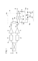
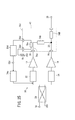
第1の実施の形態に係るドハティ増幅器用合成器(以下、単に第1合成器10Aと記す)について図1〜図4Bを参照しながら説明する。
A Doherty amplifier combiner (hereinafter simply referred to as a
第1合成器10Aは、図1に示すように、キャリア増幅器12とピーク増幅器14とを有するドハティ増幅器16の出力に接続され、キャリア増幅器12からの出力とピーク増幅器14からの出力とを合成する回路である。
As shown in FIG. 1, the
ドハティ増幅器16は、図1に示すように、入力端子18からの入力信号を2つに分配する信号分配器20と、該信号分配器20の一方の出力とキャリア増幅器12の入力とのインピーダンス整合をとるキャリア側インピーダンス整合部22と、AB級にバイアスされた上述のキャリア増幅器12(入力電力レベルが低いときから動作する)と、信号分配器20の他方の出力とピーク増幅器14の入力とのインピーダンス整合をとるピーク側インピーダンス整合部24と、B級又はC級にバイアスされた上述のピーク増幅器14(入力電力レベルが十分高いときに動作する)とを有する。
As shown in FIG. 1, the
そして、第1合成器10Aは、キャリア増幅器12からの出力が入力されるキャリア側入力端子26と、ピーク増幅器14からの出力が入力されるピーク側入力端子28と、キャリア増幅器12からの出力とピーク増幅器14からの出力とを合成した信号が出力される出力端子30と、キャリア増幅器12からの出力とピーク増幅器14からの出力との合成点32と、キャリア側入力端子26と合成点32との間に接続された第1λ/4線路34Aと、合成点32と出力端子30との間に接続された第2λ/4線路34Bと、第2λ/4線路34Bと電磁結合する第3λ/4線路34Cとを有する。第3λ/4線路34Cの一端に第1モニタ端子36aが接続され、第3λ/4線路34Cの他端に第1終端端子38aを介して終端抵抗Reが接続されている。つまり、第2λ/4線路34Bと第3λ/4線路34Cとで1つの方向性結合器(第1方向性結合器40A)が構成されている。
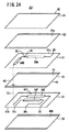
The
さらに、この第1合成器10Aは、第1方向性結合器40Aと共に1つの誘電体基板42内に一体化して形成されている。すなわち、第1合成器10Aは、図2に示すように、複数の誘電体層が積層、焼成一体化された誘電体基板42を有し、該誘電体基板42の第1側面42aには、少なくともキャリア側入力端子26とピーク側入力端子28が形成され、誘電体基板42の第2側面42b(第1側面42aと対向する側面)には、少なくとも出力端子30と第1モニタ端子36aと第1終端端子38aとが形成されている。また、誘電体基板42の第3側面42cと第4側面42d(第3側面42cと対向する側面)にはそれぞれシールド端子44が形成されている。
Further, the
そして、図3に示すように、誘電体基板42内において、キャリア側入力端子26とピーク側入力端子28間に第1λ/4線路34Aが接続され、ピーク側入力端子28(合成点32を兼ねる)と出力端子30間に第2λ/4線路34Bが接続され、第1モニタ端子36aと第1終端端子38a間に第3λ/4線路34Cが接続され、1つのチップとして構成されている。
As shown in FIG. 3, in the
具体的には、誘電体基板42は、上から順に、第1誘電体層S1〜第6誘電体層S6が積み重ねられて構成されている。これらの第1誘電体層S1〜第6誘電体層S6は、1枚あるいは複数枚の層にて構成される。
Specifically, the
第1合成器10Aは、誘電体基板42の上部(上面あるいは上面に近い誘電体層の主面)に上部シールド電極46aが形成され、誘電体基板42の下部(下面あるいは下面に近い誘電体層の主面)に下部シールド電極46bが形成されている。すなわち、第2誘電体層S2の主面に上部シールド電極46aが形成され、第6誘電体層S6の主面に下部シールド電極46bが形成されている。これら上部シールド電極46a及び下部シールド電極46bはシールド端子44に接続されている。
In the
また、第1合成器10Aは、第3誘電体層S3の主面に第1λ/4線路34Aが形成され、第5誘電体層S5の主面に、第1方向性結合器40Aを構成する第2λ/4線路34Bと第3λ/4線路34Cが形成され、第3誘電体層S3と第5誘電体層S5の間の第4誘電体層S4の主面に内層シールド電極48が形成されている。この内層シールド電極48はシールド端子44に接続されている。
In the
一方、第1モニタ端子36aには、図1に示すように、第1モニタ回路50aが電気的に接続されている。この第1モニタ回路50aは、合成点32から出力端子30にかけて流れる信号のレベルをモニタするための回路であり、第1モニタ端子36aと第1モニタ出力端子52aとの間に接続された結合コンデンサC1及びPINダイオードDaと、PINダイオードDaのバイアス回路を構成するインダクタLaと、PINダイオードDaからの検波電流を電荷として蓄積し、検波整流信号(信号レベルを示す信号:電流及び電圧)として出力するコンデンサC2とを有する。
On the other hand, as shown in FIG. 1, a
ここで、第1合成器10Aの作用・効果を、一般的なドハティ増幅器用合成器(以下、通常の合成器200と記す)と比較しながら説明する。
Here, the operation and effect of the
一般に、ドハティ増幅器16は、キャリア増幅器12がAB級にバイアスされ、ピーク増幅器14がB又はC級にバイアスされている。そのため、ピーク増幅器14が動作する入力レベルまではキャリア増幅器12が単独で動作し、キャリア増幅器12が飽和領域に入る(キャリア増幅器12の線形性が崩れ始める)と、ピーク増幅器14が動作し始め、キャリア増幅器12と共に負荷を駆動する。
In general, the
従って、例えば通常の合成器200の各部のインピーダンスを考えた場合、図4Aに示すように、出力負荷のインピーダンスをZoとしたとき、合成点32から第2λ/4線路34BをみたインピーダンスZcは、第2λ/4線路34Bの特性インピーダンスをZ2とすると、
Zc=Z22/Zo
となる。Therefore, for example, when considering the impedance of each part of the
Zc = Z2 2 / Zo
It becomes.
キャリア増幅器12から第1λ/4線路34Aをみたインピーダンス(キャリア側入力端子26のポートインピーダンスZi1)及びピーク増幅器14から第1λ/4線路34Aをみたインピーダンス(ピーク側入力端子28のポートインピーダンスZi2)については、低パワー時と高パワー時とで異なる。
The impedance of the
すなわち、低パワー時(ピーク増幅器の非動作時)においては、ポートインピーダンスZi2が実質的に無限大(オープン)となるため、第1λ/4線路34Aの特性インピーダンスをZ1としたとき、ポートインピーダンスZi1及びZi2は、
Zi1=Z12/Zc(低パワー時)
Zi2=無限大(低パワー時)
となる。That is, when the power is low (when the peak amplifier is not operating), the port impedance Zi2 is substantially infinite (open). Therefore, when the characteristic impedance of the first λ / 4
Zi1 = Z1 2 / Zc (at low power)
Zi2 = infinity (low power)
It becomes.
高パワー時(ピーク増幅器の動作時)においては、出力負荷を等しく分担するため、インピーダンスZi1及びZi2は、
Zi1=Z12/2Zc(高パワー時)
Zi2=2Zc(高パワー時)
となる。At high power (when the peak amplifier is operating), the impedances Zi1 and Zi2 are equal to share the output load.
Zi1 = Z1 2 / 2Zc (at high power)
Zi2 = 2Zc (at high power)
It becomes.
ドハティ増幅器16を周波数の高い領域で使用する場合、一般に、高パワー時におけるポートインピーダンスZi1及びZi2を等しくなるように設定することから、
Z12/2Zc=2Zc
となり、その結果、
Z1=2Zc
となる。
従って、2ZcをKとしたとき、以下の表1のような関係となる。When the
Z1 2 / 2Zc = 2Zc
And as a result,
Z1 = 2Zc
It becomes.
Therefore, when 2Zc is K, the relationship is as shown in Table 1 below.

これを知って、第1合成器10Aのインピーダンスをみた場合、図4Bに示すように、第2λ/4線路34Bの特性インピーダンスZ2は、Zc=Z22/Zoの関係から、
Z2=√(50×(K/2))
であり、第3λ/4線路34Cの特性インピーダンスZ3は、第1モニタ端子36a及び終端抵抗Reのインピーダンスが共に50オームであるから、同じく50オームとなる。すなわち、インピーダンスは、以下の表2のような関係となる。Knowing this, when looking at the impedance of the
Z2 = √ (50 × (K / 2))
The characteristic impedance Z3 of the third λ / 4
この場合、K=100オームのとき、第1方向性結合器40Aを構成する第2λ/4線路34Bの特性インピーダンスZ2と第3λ/4線路34Cの特性インピーダンスZ3が共に50オームになることから、第1方向性結合器40Aの方向性、すなわち、第1モニタ端子36aからの出力と第1終端端子38aからの出力の比を十分高めることができる。なお、Kが100オームでない場合は、特性インピーダンスZ2及びZ3が異なってくるため、その差に応じて方向性が悪くなる。
In this case, when K = 100 ohms, the characteristic impedance Z2 of the second λ / 4
このように、第1合成器10Aにおいては、ドハティ増幅器用の合成器の部分と、それに続く第1方向性結合器40Aの部分を一体に構成したので、両部分間の接続はドハティ増幅器16の製造バラツキの影響を受けることがない。これにより、第1方向性結合器40Aからの出力も安定し、よって、デジタル処理によるドハティ増幅器16の歪補正も、増幅器効率を劣化させることなく機能することとなる。
Thus, in the
また、第1合成器10Aは、ドハティ増幅器用の合成器の部分と第1方向性結合器40Aの部分を、誘電体基板42を用いたストリップライン構造で形成すると共に、それぞれを重ねるようにしたので、回路基板上での実装面積を削減することができる。このとき、合成器の部分と第1方向性結合器40Aの部分に不要な信号の漏洩が生じた場合、デジタル処理による歪補正回路への入力にノイズとなって現れ、結果として歪補正が十分行われなくなるが、この第1合成器10Aでは、第1λ/4線路34Aと、第1方向性結合器40Aを構成する第2λ/4線路34B及び第3λ/4線路34Cとの間に内層シールド電極48を形成するようにしたので、合成器の部分と第1方向性結合器40Aの部分に不要な信号の漏洩が抑制され、上述のような問題を回避することができる。
In the
さらに、合成器の部分を構成する第2λ/4線路34Bと電磁結合する第3λ/4線路34Cを形成するようにしたので、1つの誘電体基板42内に合成器の部分と方向性結合器の部分とを一体化することができる。これにより、方向性結合器に由来する損失を消去することができるため、歪補正特性を劣化させることなく、ドハティ増幅器全体の効率を向上させることができる。しかも、ドハティ増幅器16からの出力を、第2λ/4線路34Bを利用してモニタすることができるため、ドハティ増幅器16の出力信号の損失を抑制することができ、利得歪、位相歪を劣化させることなく増幅器効率を改善させることができる。
Further, since the third λ / 4
さらに、第1方向性結合器40Aに、第1モニタ端子36aを接続するようにしたので、ドハティ増幅器16の出力信号をモニタすることが可能になり、これによって利得歪、位相歪を劣化させることなく増幅器効率を改善することができる。特に、第1モニタ端子36aに第1モニタ回路50aを接続し、該第1モニタ回路50aをダイオードDaを主体した回路構成としたので、第1モニタ回路50aにおいて、ドハティ増幅器16の高周波信号が検波可能になると共に、ドハティ増幅器16の高周波信号の包絡線成分を抽出して、DPDのデジタル処理回路に入力させることができ、DPD技術を適用した利得歪・位相歪の改善を効率よく行うことができる。
Further, since the
つまり、第1合成器10Aにおいては、ドハティ増幅器16の出力信号のモニタを精度高く行うことが可能になり、これにより、ドハティ増幅器16で問題となる利得歪、位相歪を増幅器効率の低下を招くことなく改善することができる。また、ストリップライン構造の採用により、外部回路の影響を受けにくくすると共に、合成器の部分と方向性結合器の部分との間の信号の漏洩を抑制し、利得歪、位相歪を効果的に抑制することができる。
That is, in the
また、第1合成器10Aを用いることで、ドハティ増幅器16の出力歪、位相歪を抑制するために必要な部品点数を削減でき、回路の小型化・軽量化が可能になる。これにより、携帯電話の基地局アンテナ上に搭載される機器の増加に伴う建設コストの高価格化を抑制することが可能になると共に、使用部品の点数削減により、部品の接続箇所が削減されるため、信頼性が向上する。
Further, by using the
ここで、第1合成器10Aの製造方法について図5〜図8Cを参照しながら説明する。
Here, a manufacturing method of the
先ず、第1合成器10Aは、第1λ/4線路34A等を構成する導体成形体60を有する第1セラミック成形体62A(図7B参照)と、導体成形体60のない第2セラミック成形体62B(図8C参照)とを作製し、第1セラミック成形体62Aと第2セラミック成形体62Bを積層してセラミック積層体を作製し、該セラミック積層体を焼成することにより作製することができる。
First, the
導体成形体60を有する第1セラミック成形体62Aの作製方法は、先ず、図5のステップS1において、図6Aに示すように、フィルム64上に導体ペースト66を印刷法によってパターン形成した後、ステップS2において、フィルム64上に形成された導体ペースト66を加熱硬化することにより、フィルム64上に導体成形体60を形成する。
The first ceramic molded
導体ペースト66は、樹脂と銀(Ag)、金(Au)、銅(Cu)系の金属の少なくとも1種類の粉末を含む。導体ペースト66に使用される樹脂は、熱硬化性樹脂前駆体であることが好ましい。この場合、熱硬化性樹脂前駆体は、自己反応性のレゾール型フェノール樹脂であることが好ましい。フィルム64は、表面にシリコーン離型剤がコートされたPET(ポリエチレンテレフタレート)である。
The
導体ペースト66の加熱硬化時における収縮、歪を抑制するために、予めフィルム64に温度150℃で10分以上のアニール処理を施すことが好ましい。導体ペースト66は、上述したように、印刷後、加熱硬化されるが、硬化条件は、硬化剤の種類により異なり、レゾール型フェノール樹脂の場合、温度80〜150℃、時間10分〜60分で硬化させることができる。
In order to suppress shrinkage and distortion during the heat curing of the
図5のステップS3において、図6Bに示すように、鋳込み型68を組み立てて、導体成形体60が形成されたフィルム64を鋳込み型68内に設置する。
In step S3 of FIG. 5, as shown in FIG. 6B, the casting
一方、図5のステップS4及びステップS5において、鋳込み型68に注入されるスラリー70を調製する。
On the other hand, in step S4 and step S5 of FIG. 5, a
先ず、図5のステップS4において、セラミックスラリーを調製する。セラミックスラリーは、酸化チタン、酸化バリウム系粉末と焼結助剤としてのボロシリケートガラスとを混合したセラミック粉末を有する。すなわち、セラミックスラリーは、上述のセラミック粉末を100重量部と、脂肪族二塩基酸エステルを27重量部、トリアセチンを3重量部及びポリカルボン酸共重合体を3重量部からなる有機分散媒(ポリカルボン酸は有機分散剤として作用)との混合物からなる。 First, in step S4 of FIG. 5, a ceramic slurry is prepared. The ceramic slurry has a ceramic powder obtained by mixing titanium oxide or barium oxide powder and borosilicate glass as a sintering aid. That is, the ceramic slurry is an organic dispersion medium (polyester) comprising 100 parts by weight of the above ceramic powder, 27 parts by weight of an aliphatic dibasic acid ester, 3 parts by weight of triacetin, and 3 parts by weight of a polycarboxylic acid copolymer. Carboxylic acid consists of a mixture with (acting as an organic dispersant).
その後、図5のステップS5において、上述のセラミックスラリーに、ゲル化剤としてポリメチレンポリフェニルポリイソシアネートの変性物1〜10重量部とエチレングリコール0.05〜2.7重量部、反応触媒として6−ジメチルアミノ−1−ヘキサノールを0.03〜0.3重量部添加した後、攪拌して、ゲルキャスト用のスラリー70を調製する。すなわち、スラリー70は熱硬化性樹脂前駆体を含む。
Thereafter, in step S5 of FIG. 5, 1 to 10 parts by weight of a modified product of polymethylene polyphenyl polyisocyanate as a gelling agent and 0.05 to 2.7 parts by weight of ethylene glycol as a gelling agent, and 6 as a reaction catalyst. -After adding 0.03-0.3 weight part of dimethylamino-1-hexanol, it stirs and the
次に、図5のステップS6において、図6Bに示すように、鋳込み型68内にスラリー70を注入(注型)する。この注入によって、鋳込み型68の中空部にスラリー70が充填される。スラリー70は、ゲルキャスト用スラリーであることから、中空部に充填された状態でそのまま硬化される。これによって、図6Cに示すように、鋳込み型68内に第1セラミック成形体62Aが作製されることになる。
Next, in step S6 of FIG. 5, as shown in FIG. 6B, the
その後、ステップS7において、鋳込み型68を分解する。この場合、図7Aに示すように、フィルム64上に第1セラミック成形体62Aが設置された状態になっているため、第1セラミック成形体62Aをフィルム64から離型することによって、図7Bに示すように、導体成形体60が埋設された第1セラミック成形体62Aが得られる。
Thereafter, in step S7, the casting
一方、導体成形体60のない第2セラミック成形体62Bの作製方法は、図5のステップS1及びステップS2の処理を行わずに、ステップS3において、導体成形体60が形成されていないフィルム64を鋳込み型68内に設置すること以外は、上述した第1セラミック成形体62Aの作製方法と同じであり、ステップS4〜ステップS7を経ることによって、導体成形体60が存在しない第2セラミック成形体62Bを得る。すなわち、図8Aに示すように、導体成形体60が形成されていないフィルム64を鋳込み型68内に設置し、スラリー70を鋳込み型68内に鋳込んだ後に、図8Bに示すように、スラリー70を硬化(室温硬化や乾燥硬化等)する。その後、フィルム64を離型することによって、図8Cに示すように、第2セラミック成形体62Bが得られる。なお、以下の説明では、第1セラミック成形体62Aと第2セラミック成形体62Bを区別しないで言う場合はセラミック成形体62と記す。
On the other hand, in the method for producing the second ceramic molded
次に、図5のステップS8において、複数のセラミック成形体62を積層してセラミック積層体を作製する。このとき、セラミック成形体62の反応性官能基が完全に反応しない状態(室温において、注型後、1時間〜48時間経過後)で、5〜100kgf/cm2の圧力で加圧積層する。加圧力は、セラミック成形体62の強度と許容される積層ずれに応じて適宜選択される。Next, in step S8 in FIG. 5, a plurality of ceramic molded bodies 62 are laminated to produce a ceramic laminated body. At this time, pressure lamination is performed at a pressure of 5 to 100 kgf / cm 2 in a state where the reactive functional group of the ceramic molded body 62 does not completely react (at room temperature, after 1 hour to 48 hours have elapsed after casting). The applied pressure is appropriately selected according to the strength of the ceramic molded body 62 and the allowable stacking deviation.
積層時の加圧力が小さい場合は、積層ずれは小さいものの、積層時の接着不良による焼成体のデラミネーションが発生し易くなる一方、積層時の加圧力が大きい場合は、上述のデラミネーションの発生を抑制できるものの、セラミック成形体62の積層圧力による変形及び破損が発生し易くなる。しかし、上述した加圧力の範囲であれば、積層ずれとデラミネーションを抑制することができ、好ましい。また、必要に応じて、上記5〜100kgf/cm2の加圧に引き続き、50〜400kgf/cm2の加圧力で一体性を高めてもよい。When the pressing force at the time of lamination is small, the laminating deviation is small, but delamination of the fired body is likely to occur due to poor adhesion at the time of lamination. However, deformation and breakage due to the lamination pressure of the ceramic molded body 62 are likely to occur. However, if it is the range of the applied pressure mentioned above, a stacking shift and delamination can be suppressed, and it is preferable. Further, if necessary, the integrity may be enhanced by applying a pressure of 50 to 400 kgf / cm 2 following the pressurization of 5 to 100 kgf / cm 2 .
また、この際、隣り合うセラミック成形体62中の未反応の反応硬化物同士を反応させることにより、セラミック成形体62間の接着力が得られるが、より短時間で反応硬化させるために、60℃〜80℃に加温しながら積層することが好ましい。 At this time, the unreacted reaction cured products in the adjacent ceramic molded bodies 62 are reacted with each other to obtain an adhesive force between the ceramic molded bodies 62. To react and cure in a shorter time, 60 It is preferable to laminate while heating at a temperature of from -80C.
より低圧で十分なセラミック積層体を得るためには、積層時に各セラミック成形体62の界面に接着層として、スラリー70のうち、反応触媒を除いたものを塗布、印刷することが好ましい。反応触媒を添加しなくても、セラミック成形体62に残存する反応触媒の影響で、実用的な時間で反応硬化が進行する。
In order to obtain a sufficient ceramic laminate at a lower pressure, it is preferable to apply and print the
あるいは、セラミック成形体62を十分に硬化したものや、さらに乾燥した後に、セラミック成形体62と同一の無機粉末、ブチラール樹脂、アクリル樹脂、ブチルカルビトールアセテート溶剤及び/又は脂肪族二塩基酸エステル等の有機溶剤を混合した接着ペーストをセラミック成形体62上に塗布又は印刷した後、積層することも好ましい。 Alternatively, the ceramic molded body 62 is sufficiently cured, or after further drying, the same inorganic powder, butyral resin, acrylic resin, butyl carbitol acetate solvent and / or aliphatic dibasic acid ester, etc. as the ceramic molded body 62 It is also preferable that the adhesive paste mixed with the organic solvent is applied or printed on the ceramic molded body 62 and then laminated.
このようにすることで、セラミック成形体62相互の接着性が向上し、上述のデラミネーションを抑制することができる。なお、接着ペーストを使用する場合は、セラミック成形体62中に溶剤が残っていてもよいし、60℃〜100℃の温度で予め溶剤を乾燥させてもよい。溶剤を乾燥させたセラミック成形体62は可塑性が著しく低下し、ハンドリングに困難をきたすため、乾燥後のセラミック成形体62に可塑性を付与する目的で、反応硬化前のスラリーに可塑剤(DOPあるいはDBP)を1〜10重量部添加することがさらに好ましい。 By doing in this way, the adhesiveness between the ceramic molded bodies 62 improves, and the above-mentioned delamination can be suppressed. In addition, when using an adhesive paste, the solvent may remain in the ceramic molded body 62, or the solvent may be dried in advance at a temperature of 60 ° C to 100 ° C. Since the ceramic molded body 62 after drying the solvent has a markedly reduced plasticity and is difficult to handle, the plasticizer (DOP or DBP) is added to the slurry before reaction hardening for the purpose of imparting plasticity to the ceramic molded body 62 after drying. 1) to 10 parts by weight is more preferable.
次に、図5のステップS9において、セラミック積層体を乾燥した後、ステップS10において、セラミック積層体を複数のチップに分割する。その後、ステップS11において、各チップの表面や側面に端子電極を印刷により形成する。そして、ステップS12において、各チップを焼成することで、複数の第1合成器10Aが完成する。
Next, after the ceramic laminate is dried in step S9 of FIG. 5, the ceramic laminate is divided into a plurality of chips in step S10. Thereafter, in step S11, terminal electrodes are formed on the surface and side surfaces of each chip by printing. In step S12, each chip is fired to complete a plurality of
この実施の形態に係る製造方法の効果を以下に説明する。先ず、従来においては、熱可塑性樹脂を含むスラリーの乾燥収縮時に導体成形体との界面で隙間やクラックが発生したり、グリーンシートが凹凸形状になったりする。一方、本実施の形態では、スラリー70に熱硬化性樹脂前駆体を含ませて、乾燥時に熱硬化性樹脂前駆体を硬化させて三次元網目構造を生成させ、収縮を小さくすることで前記問題は解決される。
The effects of the manufacturing method according to this embodiment will be described below. First, conventionally, when a slurry containing a thermoplastic resin is dried and contracted, a gap or a crack is generated at the interface with the conductor molded body, or the green sheet becomes uneven. On the other hand, in the present embodiment, the above-mentioned problem is caused by including a thermosetting resin precursor in the
この場合、スラリー70に使用する溶剤に、熱硬化性樹脂前駆体が硬化する温度での蒸気圧が小さいものを選定し、熱硬化時の溶剤乾燥による収縮を小さくすることが望ましい。室温で硬化する樹脂を用いた場合は、特に作業や装置が簡単になる。
In this case, it is desirable to select a solvent having a low vapor pressure at a temperature at which the thermosetting resin precursor is cured as the solvent used for the
ポリウレタン樹脂は、硬化後の弾性を制御し易く、柔軟な成形体も可能となる等の利点を有する。後工程での取り扱いを考えると、あまり硬い成形体は適さない場合があり、熱硬化性樹脂は三次元網目構造をとるので一般に硬いが、ポリウレタン樹脂は、柔軟性のある成形体も可能で、特にテープ状の成形体は、柔軟性が要求される場合が多いため望ましい。また、スラリー性状の制御のため、熱可塑性樹脂を含ませてもよい。 Polyurethane resin has advantages such as easy control of elasticity after curing and also enables a flexible molded body. Considering the handling in the subsequent process, a hard molded body may not be suitable, and the thermosetting resin is generally hard because it has a three-dimensional network structure, but the polyurethane resin can also be a flexible molded body, In particular, a tape-shaped molded body is desirable because flexibility is often required. Further, a thermoplastic resin may be included for controlling the slurry properties.
従来においては、熱可塑性樹脂を含む導体ペーストが、スラリーを塗布する際に、スラリーの溶剤に溶解して、パターン形状が崩れる。一方、本実施の形態においては、導体ペースト66に熱硬化性樹脂前駆体を含ませているため、耐溶剤性が向上し、パターン形状の崩れは生じない。
Conventionally, when a conductive paste containing a thermoplastic resin is applied to a slurry, it is dissolved in the solvent of the slurry and the pattern shape is destroyed. On the other hand, in the present embodiment, since the thermosetting resin precursor is included in the
熱硬化性樹脂前駆体は、硬化後は三次元の網目構造となり、元に戻らないため、硬化後は、溶剤への再溶解性がなくなり、一般に、熱可塑性樹脂よりも耐溶剤性が高い。 Since the thermosetting resin precursor has a three-dimensional network structure after curing and does not return to its original state, it does not have re-solubility in a solvent after curing, and generally has higher solvent resistance than a thermoplastic resin.
熱硬化性樹脂前駆体の中では、フェノール樹脂、エポキシ樹脂、ポリエステル樹脂が硬化前プレポリマーの分子量の制御ができ、ペースト性状のコントロールが可能なため、好適である。なお、熱可塑性樹脂をペースト性状の制御のために、熱硬化性樹脂と一緒に含めるようにしてもよい。 Among thermosetting resin precursors, phenol resin, epoxy resin, and polyester resin are preferable because they can control the molecular weight of the prepolymer before curing and can control the paste properties. In addition, you may make it include a thermoplastic resin with a thermosetting resin for control of paste property.
特に、エポキシ樹脂、フェノール樹脂は、硬化剤が必要なく、加熱するだけで硬化するタイプがあり、導体ペースト66の効率的な使用に適する。つまり、硬化剤の添加が必要な他の熱硬化性樹脂前駆体は、導体ペースト66を印刷する前に、硬化剤を混合する必要があるが、混合すると保存がきかない。従って、印刷後に残った導体ペースト66を回収して保存する必要のある印刷法によって導体ペースト66を印刷する場合は、硬化剤を混合する必要がない熱硬化型エポキシ樹脂、熱硬化型フェノール樹脂が好適である。
In particular, epoxy resins and phenol resins do not require a curing agent and are of a type that cures only by heating and are suitable for efficient use of the
従来において、熱可塑性樹脂をバインダとするセラミック成形体は、該セラミック成形体の密度ばらつきが発生し易く、そのために、焼成後のセラミック焼成体の寸法ばらつきが大きく、埋設された導体成形体の焼成寸法のばらつきも大きくなる。一方、本実施の形態においては、熱硬化性樹脂前駆体をバインダに使用して導体成形体60を埋設した第1セラミック成形体62Aを得ることにより、焼成ばらつきを小さくすることができる。例えば第1セラミック成形体62Aの焼成後の寸法は、第1セラミック成形体62Aのうち、導体成形体60を除く部分の生密度により主に決まる。これは第1セラミック成形体62Aのセラミック焼成体の構造は空隙が非常に少ないのに対し、第1セラミック成形体62Aの上記部分は空隙が多いため、その空隙量の多少が、焼成中の収縮量を決めるからである。
Conventionally, a ceramic molded body using a thermoplastic resin as a binder is likely to have a density variation of the ceramic molded body. Therefore, the dimensional variation of the fired ceramic sintered body is large, and the embedded conductor molded body is fired. Variations in dimensions also increase. On the other hand, in the present embodiment, by using the thermosetting resin precursor as a binder to obtain the first ceramic molded
従来の熱可塑性樹脂をバインダとして含むスラリーは、溶媒を乾燥してセラミック成形体を得るが、乾燥する際の塗工比(スラリー体積と成形後の成形体体積の比)が大きく、この大きな塗工比が成形体密度のばらつきの原因となる。しかし、本実施の形態のように、熱硬化性樹脂前駆体をスラリー70のバインダとして使用した場合は、溶剤を含んだままでも硬化するため、塗工比を小さくすることができ、生密度のばらつきを小さくすることができる。その結果、焼成後の寸法ばらつきが小さくなり、埋設した導体成形体60の寸法ばらつきも小さくすることができる。
A slurry containing a conventional thermoplastic resin as a binder obtains a ceramic molded body by drying the solvent. However, the coating ratio (ratio of the slurry volume and the molded body volume after molding) during drying is large. The work ratio causes variation in the density of the compact. However, when the thermosetting resin precursor is used as the binder of the
次に、第2の実施の形態に係るドハティ増幅器用合成器(以下、第2合成器10Bと記す)について図9〜図11を参照しながら説明する。
Next, a Doherty amplifier combiner (hereinafter referred to as a
この第2合成器10Bは、上述した第1合成器10Aとほぼ同様の構成を有するが、図9に示すように、第1モニタ端子36aと第3λ/4線路34Cとの間に第4λ/4線路34Dを接続した点で異なる。
The
すなわち、第2合成器10Bは、図10に示すように、誘電体基板42が、上から順に、第1誘電体層S1〜第8誘電体層S8が積み重ねられて構成され、第7誘電体層の主面に第4λ/4線路34Dが形成され、第4誘電体層S4の主面に第1内層シールド電極48aが形成され、第6誘電体層S6の主面に第2内層シールド電極48bが形成され、第8誘電体層S8の主面に下部シールド電極46bが形成されている。第4λ/4線路34Dの一端は第1モニタ端子36aに接続され、第4λ/4線路34Dの他端は第5誘電体層S5及び第6誘電体層S6を貫通するビアホール72を介して第3λ/4線路34Cの一端に接続されている。また、第1内層シールド電極48a及び第2内層シールド電極48bはシールド端子44に接続されている。
That is, as shown in FIG. 10, the
このように、第2合成器10Bは、上述した第1合成器10Aと同様に、デジタル処理によるドハティ増幅器16の歪補正も、増幅器効率を劣化させることなく機能することとなる。また、回路基板上での実装面積を削減することができる。この第2合成器10Bでは、第1λ/4線路34Aと、第1方向性結合器40Aを構成する第2λ/4線路34B及び第3λ/4線路34Cとの間に第1内層シールド電極48aを形成し、第3λ/4線路34Cと第4λ/4線路34Dとの間にも第2内層シールド電極48bを形成するようにしたので、合成器の部分と第1方向性結合器40Aの部分との間、並びに第1方向性結合器40Aの部分と第4λ/4線路34Dでの不要な信号の漏洩を抑制することができ、デジタル処理による歪補正回路へのノイズの混入を抑圧することができる。
As described above, in the
さらに、1つの誘電体基板42内に合成器の部分と方向性結合器の部分とを一体化することができため、方向性結合器に由来する損失を消去することができ、歪補正特性を劣化させることなく、ドハティ増幅器16全体の効率を向上させることができる。
Furthermore, since the synthesizer portion and the directional coupler portion can be integrated into one
ここで、第2合成器10Bのインピーダンスの関係について説明すると、この第2合成器10Bでは、図11にも示すように、第3λ/4線路34Cと第1モニタ端子36a間に第4λ/4線路34Dを接続したため、第3λ/4線路34Cと第4λ/4線路との中間点からみた第3λ/4線路34Cのインピーダンスを合成点32からみた第2λ/4線路34BのインピーダンスZcと同等にすることができると共に、以下の表3に示すように、モニタ対象の第2λ/4線路34B、第1方向性結合器40Aの第3λ/4線路34C及び第4λ/4線路34Dの各特性インピーダンスZ2、Z3及びZ4を共に√(50×(K/2))にすることができる。
Here, the relationship of the impedance of the
これにより、Kが50オームや100オームでなくても、第1方向性結合器40Aの方向性を十分に高めることができる。 Thereby, even if K is not 50 ohms or 100 ohms, the directivity of 40 A of 1st directional couplers can fully be improved.
次に、第3の実施の形態に係るドハティ増幅器用合成器(以下、第3合成器10Cと記す)について図12及び図13を参照しながら説明する。 Next, a Doherty amplifier combiner (hereinafter referred to as a third combiner 10C) according to a third embodiment will be described with reference to FIGS.
この第3合成器10Cは、上述した第2合成器10Bとほぼ同様の構成を有するが、図12に示すように、第1終端端子38aと第3λ/4線路34Cとの間に第4λ/4線路34Dを接続した点で異なる。
The third synthesizer 10C has substantially the same configuration as the above-described
すなわち、第3合成器10Cは、図13に示すように、第4λ/4線路34Dの一端は第1終端端子38aに接続され、第3λ/4線路34Cの一端は第1モニタ端子36aに接続され、第4λ/4線路34Dの他端は第5誘電体層S5及び第6誘電体層S6を貫通するビアホール72を介して第3λ/4線路34Cの他端に接続されている。
That is, in the third combiner 10C, as shown in FIG. 13, one end of the fourth λ / 4
このように、第3合成器10Cは、上述した第2合成器10Bと同様に、デジタル処理によるドハティ増幅器16の歪補正も、増幅器効率を劣化させることなく機能することとなる。また、回路基板上での実装面積を削減することができる。合成器の部分と第1方向性結合器40Aの部分との間、並びに第1方向性結合器40Aの部分と第4λ/4線路34Dでの不要な信号の漏洩を抑制することができ、デジタル処理による歪補正回路へのノイズの混入を抑圧することができる。
As described above, similarly to the
さらに、1つの誘電体基板42内に合成器の部分と方向性結合器の部分とを一体化することができたため、方向性結合器に由来する損失を消去することができ、歪補正特性を劣化させることなく、ドハティ増幅器全体の効率を向上させることができる。
Furthermore, since the synthesizer portion and the directional coupler portion can be integrated into one
ここで、第3合成器10Cのインピーダンスの関係について説明すると、この第3合成器10Cでは、第3λ/4線路34Cと第1終端端子38a間に第4λ/4線路34Dを接続したため、以下の表4に示すように、第2λ/4線路34B、第3λ/4線路34C及び第4λ/4線路34Dの各特性インピーダンスZ2、Z3及びZ4を√(50×(K/2))にすることができる。但し、第3λ/4線路34Cと第4λ/4線路との中間点からみた第3λ/4線路34Cのインピーダンスは、合成点32からみた第2λ/4線路34BのインピーダンスZcと異なる。そのため、上述した第2合成器10Bとは異なり、第1方向性結合器40Aの方向性は幾分悪くなる。
Here, the impedance relationship of the third synthesizer 10C will be described. In the third synthesizer 10C, the fourth λ / 4
次に、第4の実施の形態に係るドハティ増幅器用合成器(以下、第4合成器10Dと記す)について図14及び図15を参照しながら説明する。
Next, a Doherty amplifier combiner (hereinafter referred to as a
この第4合成器10Dは、上述した第1合成器10Aとほぼ同様の構成を有するが、図14に示すように、第3λ/4線路34Cが第1λ/4線路34Aと電磁結合されている点で異なる。すなわち、第4合成器10Dは、第1方向性結合器40Aに代えて、第1λ/4線路34Aと第3λ/4線路34Cとによる第2方向性結合器40Bを有する。
The
第4合成器10Dは、図15に示すように、第3誘電体層S3の主面に第1λ/4線路34Aと第3λ/4線路34Cが形成され、第5誘電体層S5の主面に第2λ/4線路34Bが形成され、第4誘電体層S4の主面にシールド端子44に接続された内層シールド電極48が形成されている。そして、キャリア側入力端子26とピーク側入力端子28間に第1λ/4線路34Aが接続され、ピーク側入力端子28(合成点32を兼ねる)と出力端子30間に第2λ/4線路34Bが接続され、誘電体基板42の第2側面42bに形成された第2モニタ端子36bと第2終端端子38b間に第3λ/4線路34Cが接続されて、1つのチップとして構成されている。
As shown in FIG. 15, in the
一方、図14に示すように、第2モニタ端子36bと第2モニタ出力端子52b間には第2モニタ回路50bが電気的に接続されている。この第2モニタ回路50bは、キャリア側入力端子26から合成点32にかけて流れる信号のレベルをモニタするための回路であり、上述した第1モニタ回路50aと同様の構成を有する。
On the other hand, as shown in FIG. 14, a
この第4合成器10Dにおいては、キャリア増幅器12からの出力信号がモニタ可能となり、これにより、キャリア増幅器12の利得、位相を適宜補正することが可能となるため、ドハティ増幅器16を使用する上で問題となる利得歪、位相歪を、増幅器効率の低下を招くことなく改善することができる。
In this
また、第1合成器10Aの場合と同様に、ストリップライン構造の採用により、外部回路の影響を受けにくくすると共に、合成器の部分と方向性結合器の部分との間の信号の漏洩を抑制し、利得歪、位相歪を効果的に抑制することができる。さらに、ドハティ増幅器16の出力歪、位相歪を抑制するために必要な部品点数を削減でき、回路の小型化・軽量化が可能になる。これにより、携帯電話の基地局アンテナ上に搭載される機器の増加に伴う建設コストの高価格化を抑制することが可能になると共に、使用部品の点数削減により、部品の接続箇所が削減されるため、信頼性が向上する。
As in the case of the
次に、第5の実施の形態に係るドハティ増幅器用合成器(以下、第5合成器10Eと記す)について図16〜図18を参照しながら説明する。
Next, a Doherty amplifier combiner (hereinafter referred to as a
この第5合成器10Eは、上述した第4合成器10Dとほぼ同様の構成を有するが、図16に示すように、第2モニタ端子36bと第3λ/4線路34Cとの間に第4λ/4線路34Dを接続した点で異なる。
The
第5合成器10Eは、図17に示すように、誘電体基板42が、上から順に、第1誘電体層S1〜第8誘電体層S8が積み重ねられて構成され、第7誘電体層S7の主面に第2λ/4線路34Bが形成され、第5誘電体層S5の主面に第4λ/4線路34Dが形成され、第4誘電体層S4の主面に第1内層シールド電極48aが形成され、第6誘電体層S6の主面に第2内層シールド電極48bが形成され、第8誘電体層S8の主面に下部シールド電極46bが形成されている。第4λ/4線路34Dの一端は第2モニタ端子36bに接続され、第4λ/4線路34Dの他端は第3誘電体層S3及び第4誘電体層S4を貫通するビアホール72を介して第3λ/4線路34Cの一端に接続されている。この第5合成器10Eにおいても、上述した第4合成器と同様の効果を奏する。
As shown in FIG. 17, the fifth synthesizer 10 </ b> E is configured by stacking a first dielectric layer S <b> 1 to an eighth dielectric layer S <b> 8 in order from the top, and a seventh dielectric layer S <b> 7. The second λ / 4
ここで、第5合成器10Eのインピーダンスの関係について説明すると、この第5合成器10Eでは、図18に示すように、第3λ/4線路34Cと第2モニタ端子36b間に第4λ/4線路34Dを接続したため、以下の表5に示すように、モニタ対象の第1λ/4線路34A、第2方向性結合器40Bの第3λ/4線路34C及び第4λ/4線路34Dの各特性インピーダンスをKにすることができる。これにより、Kが50オームや100オームでなくても、第2方向性結合器40Bの方向性を十分に高めることができる。
Here, the impedance relationship of the
次に、第6の実施の形態に係るドハティ増幅器用合成器(以下、第6合成器10Fと記す)について図19及び図20を参照しながら説明する。
Next, a Doherty amplifier combiner (hereinafter referred to as a
この第6合成器10Fは、上述した第5合成器10Eとほぼ同様の構成を有するが、図19に示すように、第2終端端子38bと第3λ/4線路34Cとの間に第4λ/4線路34Dを接続した点で異なる。
The
すなわち、第6合成器10Fは、図20に示すように、第4λ/4線路34Dの一端は第2終端端子38bに接続され、第3λ/4線路34Cの一端は第2モニタ端子36bに接続され、第4λ/4線路34Dの他端は第3誘電体層S3及び第4誘電体層S4を貫通するビアホール72を介して第3λ/4線路34Cの他端に接続されている。この第6合成器10Fにおいても、上述した第5合成器10Eと同様の効果を奏する。
That is, in the
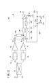
次に、第7の実施の形態に係るドハティ増幅器用合成器(以下、第7合成器10Gと記す)について図21を参照しながら説明する。
Next, a Doherty amplifier combiner (hereinafter referred to as a
この第7合成器10Gは、図21に示すように、第1合成器10Aと第4合成器10Dとが組み合わされた構成を有する。すなわち、2つの第3λ/4線路34Ca及び34Cbを有し、第2λ/4線路34Bと該第2λ/4線路34Bと電磁結合する一方の第3λ/4線路34Caとによる第1方向性結合器40Aと、第1λ/4線路34Aと該第1λ/4線路34Aと電磁結合する他方の第3λ/4線路34Cbとによる第2方向性結合器40Bとを有する。この第7合成器10Gにおいては、第1合成器10Aによる効果と第4合成器10Dによる効果を併せ持つ。
As shown in FIG. 21, the
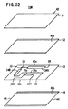
次に、第8の実施の形態に係るドハティ増幅器用合成器(以下、第8合成器10Hと記す)について図22を参照しながら説明する。
Next, a Doherty amplifier combiner (hereinafter referred to as an
この第8合成器10Hは、図22に示すように、第2合成器10Bと第5合成器10Eとが組み合わされた構成を有する。すなわち、2つの第3λ/4線路34Ca及び34Cbと2つの第4λ/4線路34Da及び34Dbとを有し、第2λ/4線路34Bと該第2λ/4線路34Bと電磁結合する一方の第3λ/4線路34Caとによる第1方向性結合器40Aと、第1λ/4線路34Aと該第1λ/4線路34Aと電磁結合する他方の第3λ/4線路34Cbとによる第2方向性結合器40Bとを有する。一方の第4λ/4線路34Daは第1方向性結合器40Aと第1モニタ端子36a間に接続され、他方の第4λ/4線路34Dbは第2方向性結合器40Bと第2モニタ端子36b間に接続されている。この第8合成器10Hにおいては、第2合成器10Bによる効果と第5合成器10Eによる効果を併せ持つ。
As shown in FIG. 22, the
次に、第9の実施の形態に係るドハティ増幅器用合成器(以下、第9合成器10Iと記す)について図23及び図24を参照しながら説明する。 Next, a Doherty amplifier combiner (hereinafter referred to as a ninth combiner 10I) according to a ninth embodiment will be described with reference to FIGS.
この第9合成器10Iは、図23に示すように、第2λ/4線路34Bと出力端子30との間に第5λ/4線路34Eが形成され、該第5λ/4線路34Eと電磁結合する第6λ/4線路34Fが形成されている。第6λ/4線路34Fの一端に第3モニタ端子36cが接続され、第6λ/4線路34Fの他端に第3終端端子38cを介して終端抵抗Reが接続されている。つまり、第5λ/4線路34Eと第6λ/4線路34Fとで1つの方向性結合器(第3方向性結合器40C)が構成されている。
In the ninth combiner 10I, as shown in FIG. 23, a fifth λ / 4
すなわち、第9合成器10Iは、図24に示すように、誘電体基板42が、上から順に、第1誘電体層S1〜第6誘電体層S6が積み重ねられて構成され、第3誘電体層S3の主面に第1λ/4線路34A及び第2λ/4線路34Bが形成され、第5誘電体層S5の主面に第5λ/4線路34E及び第6λ/4線路34Fが形成されている。第1λ/4線路34Aの一端はキャリア側入力端子26に接続され、第1λ/4線路34Aの他端及びピーク側入力端子28は合成点32を介して第2λ/4線路34Bの一端に接続され、第2λ/4線路34Bの他端は第3誘電体層S3及び第4誘電体層S4を貫通するビアホール72を介して第5λ/4線路34Eの一端に接続され、第5λ/4線路34Eの他端は出力端子30に接続され、第6λ/4線路34Fの一端は第3モニタ端子36cに接続され、第6λ/4線路34Fの他端は第3終端端子38cに接続されている。
That is, as shown in FIG. 24, the ninth synthesizer 10I is configured by stacking the first dielectric layer S1 to the sixth dielectric layer S6 in order from the top, and the third
図23に示すように、第3モニタ端子36cと第3モニタ出力端子52c間には、第3モニタ回路50cが電気的に接続されている。この第3モニタ回路50cは、合成点32から出力端子30にかけて流れる信号のレベルをモニタするための回路であり、上述した第1モニタ回路50aと同様の構成を有する。
As shown in FIG. 23, the
この第9合成器10Iにおいても、第1合成器10Aと同様に、ドハティ増幅器16の出力信号のモニタを精度高く行うことが可能になり、よってドハティ増幅器16で問題となる利得歪、位相歪を増幅器効率の低下を招くことなく改善することができる。また、ストリップライン構造の採用により、外部回路の影響を受けにくくすると共に、合成器の部分と方向性結合器の部分との間の信号の漏洩を抑制し、利得歪、位相歪を効果的に抑制することができる。
In the ninth combiner 10I as well as the
また、第9合成器10Iを用いることで、ドハティ増幅器16の出力歪、位相歪を抑制するために必要な部品点数を削減でき、回路の小型化・軽量化が可能になる。これにより、携帯電話の基地局アンテナ上に搭載される機器の増加に伴う建設コストの高価格化を抑制することが可能になると共に、使用部品の点数削減により、部品の接続箇所が削減されるため、信頼性が向上する。
Further, by using the ninth synthesizer 10I, the number of parts necessary for suppressing the output distortion and phase distortion of the
次に、第10の実施の形態に係るドハティ増幅器用合成器(以下、第10合成器10Jと記す)について図25及び図26を参照しながら説明する。
Next, a Doherty amplifier combiner (hereinafter referred to as a
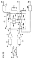
この第10合成器10Jが適用されるドハティ増幅器16は、第1合成器10Aが適用されるドハティ増幅器16とほぼ同様の構成を有するが、図25に示すように、キャリア増幅器12のゲートバイアス電圧を制御するための第1制御器74aを有する点で異なる。
The
そして、第10合成器10Jは、図25に示すように、第1合成器10Aと同様のキャリア側入力端子26、ピーク側入力端子28及び出力端子30と、キャリア増幅器12からのキャリア信号の振幅情報を出力するための第4モニタ端子36dと、キャリア側入力端子26と第1λ/4線路34Aとの間の第1線路76aに平行して配置され、第1線路76aと電磁気的に結合された第1モニタ線路78aとを有する。
Then, as shown in FIG. 25, the
すなわち、第10合成器10Jは、図26に示すように、誘電体基板42の第1側面42aに少なくともキャリア側入力端子26とピーク側入力端子28が形成され、誘電体基板42の第2側面42bには、少なくとも出力端子30と第4モニタ端子36dと第4終端端子38dとが形成されている。
That is, in the
誘電体基板42は、上から順に、第1誘電体層S1〜第4誘電体層S4が積み重ねられて構成され、第3誘電体層の主面に第1λ/4線路34A及び第2λ/4線路34Bと、キャリア側入力端子26から第1λ/4線路34Aの一端に延びる第1線路76aと電磁結合される第1モニタ線路78aとが形成されている。第1λ/4線路34Aの他端及びピーク側入力端子28は合成点32を介して第2λ/4線路34Bの一端に接続され、第2λ/4線路34Bの他端は出力端子30に接続され、第1モニタ線路78aの一端は第4モニタ端子36dに接続され、第1モニタ線路78aの他端は第4終端端子38dに接続されている。
The
図25に示すように、第4モニタ端子36dには、第4モニタ回路50dが電気的に接続されている。この第4モニタ回路50dは、キャリア側入力端子26に入力されたキャリア増幅器12からのキャリア信号の振幅レベルをモニタするための回路であり、第1モニタ回路50aと同様の構成を有する。第4モニタ回路50dの第4モニタ出力端子52dから出力される信号は第1制御器74aに入力される。第1制御器74aは、入力された第4モニタ出力端子52dからの信号のレベルに応じて、キャリア増幅器12のゲートバイアス電圧を調整する。
As shown in FIG. 25, a
このように、第10合成器10Jにおいては、キャリア増幅器12の振幅に対する飽和特性をモニタすることが可能となるため、キャリア増幅器12の入力レベルに対する出力レベルを確認することができる。飽和領域をモニタすることにより、キャリア増幅器12のゲートバイアス電圧の制御を行うことで、ドハティ増幅器16のAM/AM特性を改善させることが可能であり、従来のドハティ増幅器と比較して効率低下することなく低歪化が可能となる。また、第4モニタ回路50dをダイオードDaを主体した回路構成としたので、第4モニタ回路50dにおいて、キャリア増幅器12の高周波信号が検波可能になる。ゲートバイアス電圧の制御に用いる信号としては、振幅情報のみが必要であるが、第4モニタ回路50dを用いることで、例えば半波整流された信号を得ることができ、キャリア増幅器12のゲートバイアス電圧の制御に必要な振幅情報を第1制御器74aに供給することができる。
Thus, in the
次に、第11の実施の形態に係るドハティ増幅器用合成器(以下、第11合成器10Kと記す)について図27及び図28を参照しながら説明する。
Next, a Doherty amplifier combiner (hereinafter referred to as an
この第11合成器が適用されるドハティ増幅器10Kは、第1合成器10Aが適用されるドハティ増幅器16とほぼ同様の構成を有するが、図27に示すように、ピーク増幅器14のゲートバイアス電圧を制御するための第2制御器74bを有する点で異なる。
The Doherty amplifier 10K to which the eleventh synthesizer is applied has substantially the same configuration as the
そして、第11合成器10Kは、図27に示すように、第1合成器10Aと同様のキャリア側入力端子26、ピーク側入力端子28及び出力端子30と、ピーク増幅器14からのピーク信号の振幅情報を出力するための第5モニタ端子36eと、ピーク側入力端子28と第1λ/4線路34Aとの間の第2線路76bに平行して配置され、第2線路76bと電磁気的に結合された第2モニタ線路78bとを有する。
As shown in FIG. 27, the
すなわち、第11合成器10Kは、図28に示すように、誘電体基板42の第1側面42aに少なくともキャリア側入力端子26とピーク側入力端子28が形成され、誘電体基板42の第2側面42bに少なくとも出力端子30と第5モニタ端子36eと第5終端端子38eとが形成されている。
That is, in the
誘電体基板42は、上から順に、第1誘電体層S1〜第4誘電体層S4が積み重ねられて構成され、第3誘電体層S3の主面に第1λ/4線路34A及び第2λ/4線路34Bと、ピーク側入力端子28から第1λ/4線路34Aの他端に延びる第2線路76bと電磁結合される第2モニタ線路78bとが形成されている。第1λ/4線路34Aの一端はキャリア側入力端子26に接続され、第1λ/4線路34Aの他端及びピーク側入力端子28は合成点32を介して第2λ/4線路34Bの一端に接続され、第2λ/4線路34Bの他端は出力端子30に接続され、第2モニタ線路78bの一端は第5モニタ端子36eに接続され、第2モニタ線路78bの他端は第5終端端子38eに接続されている。
The
図27に示すように、第5モニタ端子36eには、第5モニタ回路50eが電気的に接続されている。この第5モニタ回路50eは、ピーク側入力端子28に入力されたピーク増幅器14からのピーク信号のレベルをモニタするための回路であり、第1モニタ回路50aと同様の構成を有する。第5モニタ回路50eの第5モニタ出力端子52eから出力される信号は第2制御器74bに入力される。第2制御器74bは、入力された第5モニタ出力端子52eからの信号のレベルに応じて、ピーク増幅器14のゲートバイアス電圧を調整する。
As shown in FIG. 27, a
このように、第11合成器10Kにおいては、ピーク増幅器14からの出力信号がモニタ可能となり、これにより、ピーク増幅器14のゲートバイアス電圧を適宜補正することが可能となるため、ドハティ増幅器16を使用する上で問題となる利得歪を、増幅器効率の低下を招くことなく改善することができる。また、第5モニタ回路50eを用いることで、例えば半波整流された信号を得ることができ、ピーク増幅器14のゲートバイアス電圧の制御に必要な振幅情報を第2制御器74bに供給することができる。
In this way, in the
次に、第12の実施の形態に係るドハティ増幅器用合成器(以下、第12合成器10Lと記す)について図29〜図30を参照しながら説明する。
Next, a Doherty amplifier combiner (hereinafter referred to as a
この第12合成器10Lが適用されるドハティ増幅器16は、図29に示すように、キャリア増幅器12のゲートバイアス電圧を制御するための第1制御器74aと、ピーク増幅器14のゲートバイアス電圧を制御するための第2制御器74bとを有する。
As shown in FIG. 29, the
そして、第12合成器10Lは、第10合成器10Jと第11合成器10Kとが組み合わされた構成を有する。具体的には、図30に示すように、誘電体基板42の第1側面42aに少なくともキャリア側入力端子26とピーク側入力端子28が形成され、誘電体基板42の第2側面42bに少なくとも出力端子30、第4モニタ端子36d、第4終端端子38d、第5モニタ端子36e及び第5終端端子38eが形成されている。
The
誘電体基板42は、上から順に、第1誘電体層S1〜第4誘電体層S4が積み重ねられて構成され、第3誘電体層S3の主面に第1λ/4線路34A、第2λ/4線路34B、第1モニタ線路78a及び第2モニタ線路78bが形成されている。第1λ/4線路34Aの一端はキャリア側入力端子26に接続され、第1λ/4線路34Aの他端及びピーク側入力端子28は合成点32を介して第2λ/4線路34Bの一端に接続され、第2λ/4線路34Bの他端は出力端子30に接続されている。第1モニタ線路78aの一端は第4モニタ端子36dに接続され、第1モニタ線路78aの他端は第4終端端子38dに接続され、第2モニタ線路78bの一端は第5モニタ端子36eに接続され、第2モニタ線路78bの他端は第5終端端子38eに接続されている。また、第4モニタ端子36dには第4モニタ回路50dが接続され、第5モニタ端子36eには第5モニタ回路50eが接続されている。第4モニタ回路50dの第4モニタ出力端子52dから出力される信号は第1制御器74aに入力され、第5モニタ回路50eの第5モニタ出力端子52eから出力される信号は第2制御器74bに入力される。
The
この第12合成器10Lにおいては、第10合成器10Jによる効果と第11合成器10Kによる効果を併せ持つ。すなわち、キャリア増幅器12のゲートバイアス電圧の制御に加え、ピーク増幅器14のゲートバイアス電圧の制御も行うことができるため、ドハティ増幅器16の出力飽和点を向上させることができる。その結果、DPD等の歪補償器でのバックオフ点を改善でき、さらなる高効率化が可能となる。
The
次に、第13の実施の形態に係るドハティ増幅器用合成器(以下、第13合成器10Mと記す)について図31及び図32を参照しながら説明する。
Next, a Doherty amplifier combiner (hereinafter referred to as a
この第13合成器10Mは、図31に示すように、第1合成器10Aと同様のキャリア側入力端子26、ピーク側入力端子28及び出力端子30と、ドハティ増幅器16の出力信号の振幅情報を出力するための第6モニタ端子36fと、出力端子30と第2λ/4線路34Bとの間の第3線路76cに平行して配置され、且つ、第3線路76cと電磁気的に結合された第3モニタ線路78cとを有する。
As shown in FIG. 31, the
すなわち、第13合成器10Mは、図32に示すように、誘電体基板42の第1側面42aに少なくともキャリア側入力端子26とピーク側入力端子28が形成され、誘電体基板42の第2側面42bに少なくとも出力端子30と第6モニタ端子36fと第6終端端子38fとが形成されている。
That is, in the
誘電体基板42は、上から順に、第1誘電体層S1〜第4誘電体層S4が積み重ねられて構成され、第3誘電体層S3の主面に第1λ/4線路34A及び第2λ/4線路34Bと、第2λ/4線路34Bの一端から出力端子30に延びる第3線路76cと電磁結合される第3モニタ線路78cとが形成されている。第1λ/4線路34Aの一端はキャリア側入力端子26に接続され、第1λ/4線路34Aの他端及びピーク側入力端子28は合成点32を介して第2λ/4線路の他端に接続され、第3モニタ線路78cの一端は第6モニタ端子36fに接続され、第3モニタ線路78cの他端は第6終端端子38fに接続されている。
The
図31に示すように、第6モニタ端子36fと第6モニタ出力端子52f間には、第6モニタ回路50fが電気的に接続されている。この第6モニタ回路50fは、ドハティ増幅器16の出力レベルをモニタするための回路であり、第1モニタ回路50aと同様の構成を有する。
As shown in FIG. 31, a
この第13合成器10Mにおいては、ドハティ増幅器16のAM/AM歪(利得歪)補正用信号、並びにAP/PM歪(振幅位相歪)補正用信号をモニタすることができる。すなわち、第1合成器10Aと同様に、ドハティ増幅器16の出力信号のモニタを精度高く行うことが可能になり、これにより、ドハティ増幅器16で問題となる利得歪、位相歪を増幅器効率の低下を招くことなく改善することができる。また、ストリップライン構造の採用により、外部回路の影響を受けにくくすると共に、合成器の部分と方向性結合器の部分との間の信号の漏洩を抑制し、利得歪、位相歪を効果的に抑制することができる。
In the
また、第13合成器10Mを用いることで、ドハティ増幅器16の出力歪、位相歪を抑制するために必要な部品点数を削減でき、回路の小型化・軽量化が可能になる。これにより、携帯電話の基地局アンテナ上に搭載される機器の増加に伴う建設コストの高価格化を抑制することが可能になると共に、使用部品の点数削減により、部品の接続箇所が削減されるため、信頼性が向上する。
Further, by using the
ここで、第1合成器10A〜第13合成器10Mに関し、2つの好ましい変形例(第1変形例及び第2変形例)について、図33及び図34を参照しながら説明する。
Here, regarding the
先ず、第1変形例に係る合成器10aは、例えば第1合成器10Aに適用した場合を主体に説明すると、図33に示すように、キャリア側入力端子26と第1λ/4線路34Aとの間に第1結合コンデンサC3aを接続し、ピーク側入力端子28と第1λ/4線路34Aとの間に第2結合コンデンサC3bを接続する。
First, the
第1合成器10Aのキャリア側入力端子26にはキャリア増幅器12のドレイン端子が接続され、ピーク側入力端子28にはピーク増幅器14のドレイン端子が接続されることになるため、上述の第1結合コンデンサC3a及び第2結合コンデンサC3bを接続することにより、キャリア増幅器12及びピーク増幅器14の各ドレイン端子に供給される直流電力を第1合成器10Aと切り離し、高周波成分のみを第1合成器10Aに入力することができる。特に、この変形例1では、誘電体基板42内に、上述した第1λ/4線路34A、第2λ/4線路34B及び第3λ/4線路34Cと共に第1結合コンデンサC3a及び第2結合コンデンサC3bを形成して一体化したので、小型化を図ることができる。
Since the drain terminal of the
第2変形例に係る合成器10bは、図34に示すように、1つのピーク増幅器14に対して複数のキャリア増幅器12を並列に接続したN−Wayドハティ増幅器(Nは3以上の整数)に接続されるもので、例えば第12合成器10Lに適用した場合を主体に説明すると、複数のキャリア増幅器12に対応した複数のキャリア側入力端子26と、1つのピーク増幅器14に対応した1つのピーク側入力端子28と、1つの出力端子30と、複数のキャリア側入力端子26と1つの合成点32との間にそれぞれ接続された複数の第1λ/4線路34Aと、合成点32と出力端子30との間に接続された1つの第2λ/4線路34Bとを有する。
As shown in FIG. 34, the
また、この第2変形例に係る合成器10bは、各キャリア側入力端子26とそれぞれ対応する第1λ/4線路34Aとの間の各第1線路76aに平行して配置され、対応する第1線路76aにそれぞれ電磁結合された複数の第1モニタ線路78aと、ピーク側入力端子28と合成点32との間の第2線路76bに平行して配置され、第2線路76bと電磁気的に結合された第2モニタ線路78bとを有する。
The
複数の第1モニタ線路78aの各一端はそれぞれ対応する第4モニタ端子36dに接続され、複数の第1モニタ線路78aの各他端はそれぞれ対応する第4終端端子38dに接続されている。また、第2モニタ線路78bの一端は第5モニタ端子36eに接続され、他端は第5終端端子38eに接続されている。そして、図34では、図示しないが、複数の第4モニタ端子36dにはそれぞれ第4モニタ回路50d(図29参照)が接続されており、各第4モニタ回路50dからの信号がそれぞれ対応する第1制御器74aに供給されるようになっている。同様に、第5モニタ端子36eにも第5モニタ回路50e(図29参照)が接続されており、該第5モニタ回路50eからの信号が第2制御器74bに供給されるようになっている。
Each one end of the plurality of
この第2変形例に係る合成器10bにおいては、複数のキャリア増幅器12に対応して複数の第1λ/4線路34Aを有することから、より広い出力範囲で高効率が得られるN−wayドハティ増幅器の利得歪、位相歪を、増幅器効率の低下を招くことなく改善することができる。
Since the
次に、第14の実施の形態に係るドハティ増幅器用合成器(以下、第14合成器10Nと記す)について図35及び図36を参照しながら説明する。
Next, a Doherty amplifier combiner (hereinafter referred to as a
この第14合成器10Nは、図35に示すように、2つのドハティ増幅器(第1ドハティ増幅器16A及び第2ドハティ増幅器16B)が並列に連結された複合ドハティ増幅器80の出力に接続され、第1ドハティ増幅器16Aの出力と第2ドハティ増幅器16Bの出力を合成する回路である。
As shown in FIG. 35, the
すなわち、複合ドハティ増幅器80は、図35に示すように、入力端子82からの入力信号を2つに分配する信号分配器84と、信号分配器84からの第1入力信号が入力される第1ドハティ増幅器16Aと、信号分配器84からの第2入力信号が入力される第2ドハティ増幅器16Bとを有する。
That is, in the
第1ドハティ増幅器16Aは、第1入力信号を2つに分配する第1信号分配器20Aと、AB級にバイアスされた第1キャリア増幅器12Aと、第1信号分配器20Aの一方の出力と第1キャリア増幅器12Aの入力とのインピーダンス整合をとる第1キャリア側インピーダンス整合部22Aと、B級又はC級にバイアスされた第1ピーク増幅器14Aと、第1信号分配器20Aの他方の出力と第1ピーク増幅器14Aの入力とのインピーダンス整合をとる第1ピーク側インピーダンス整合部24Aとを有する。
The
第2ドハティ増幅器16Bは、上述の第1ドハティ増幅器16Aと同様の第2信号分配器20B、第2キャリア増幅器12B、第2ピーク増幅器14B、第2キャリア側インピーダンス整合部22B及び第2ピーク側インピーダンス整合部24Bを有する。
The
そして、第14合成器10Nは、第1ドハティ増幅器16Aに対応した第1合成部86Aと、第2ドハティ増幅器16Bに対応した第2合成部86Bとを有する。
The
第1合成部86Aは、第1キャリア増幅器12Aからの出力が入力される第1キャリア側入力端子26aと、第1ピーク増幅器14Aからの出力が入力される第1ピーク側入力端子28aと、第1キャリア増幅器12Aからの出力と第1ピーク増幅器14Aからの出力との第1合成点32aと、第1キャリア側入力端子26aと第1合成点32aとの間に接続された一方の第1λ/4線路34Aaと、第1合成部86Aの出力が現れる第1出力ノード88aと、第1合成点32aと第1出力ノード88aとの間に接続された一方の第2λ/4線路34Baとを有する。
The
また、第2合成部86Bは、上述した第1合成部86Aと同様に、第2キャリア側入力端子26b、第2ピーク側入力端子28b、第2合成点32b、他方の第1λ/4線路34Ab、第2出力ノード88b及び他方の第2λ/4線路34Bbを有する。
Similarly to the first combining
さらに、この第14合成器10Nは、第1出力ノード88aと出力端子30間に接続された第7λ/4線路34Gと、第2出力ノード88bとGND(グランド)間に接続され、第7λ/4線路34Gと電磁結合する第8λ/4線路34Hとを有する。第7λ/4線路34Gと第8λ/4線路34Hとで1つの方向性結合器(第4方向性結合器40D)が構成されている。
Further, the
さらに、この第14合成器10Nは、第1合成部86Aと、第2合成部86Bとが第4方向性結合器40Dと共に1つの誘電体基板42内に一体化して形成されている。
Further, in the
すなわち、第14合成器10Nは、図36に示すように、誘電体基板42の第2側面42bに少なくとも第1キャリア側入力端子26aと、第1ピーク側入力端子28aと、第2キャリア側入力端子26bと、第2ピーク側入力端子28bとが形成され、誘電体基板42の第1側面42aに少なくとも出力端子30が形成されている。
That is, as shown in FIG. 36, the
誘電体基板42は、上から順に、第1誘電体層S1〜第8誘電体層S8が積み重ねられて構成されている。これらの第1誘電体層S1〜第8誘電体層S8は、1枚あるいは複数枚の層にて構成される。
The
第14合成器10Nは、第3誘電体層S3の主面に第1合成部86Aを構成する一方の第1λ/4線路34Aa、一方の第2λ/4線路34Ba及び第1合成点32aが形成され、第4誘電体層S4の主面にシールド端子44に接続された第1内層シールド電極48aが形成され、第5誘電体層S5の主面に第4方向性結合器40Dを構成する第7λ/4線路34G及び第8λ/4線路34Hが形成され、第6誘電体層S6の主面にシールド端子44に接続された第2内層シールド電極48bが形成され、第7誘電体層S7の主面に第2合成部86Bを構成する他方の第1λ/4線路34Ab、他方の第2λ/4線路34Bb及び第2合成点32bが形成されている。
In the
一方の第1λ/4線路34Aaの一端は第1キャリア側入力端子26aに接続され、一方の第2λ/4線路34Baの一端は第1合成点32aを介して一方の第1λ/4線路34Aaの他端及び第1ピーク側入力端子28aに接続され、一方の第2λ/4線路34Baの他端は第3誘電体層S3及び第4誘電体層S4を貫通する第1ビアホール72aを介して第7λ/4線路34Gの一端に接続され、第7λ/4線路34Gの他端は出力端子30に接続されている。
One end of one first λ / 4 line 34Aa is connected to the first carrier
同様に、他方の第1λ/4線路34Abの一端は第2キャリア側入力端子26bに接続され、他方の第2λ/4線路34Bbの一端は第2合成点32bを介して他方の第1λ/4線路34Abの他端及び第2ピーク側入力端子28bに接続され、他方の第2λ/4線路34Bbの他端は第5誘電体層S5及び第6誘電体層S6を貫通する第2ビアホール72bを介して第8λ/4線路34Hの一端に接続され、第8λ/4線路34Hの他端はシールド端子44に接続されている。
Similarly, one end of the other first λ / 4 line 34Ab is connected to the second carrier
一般に、携帯電話の基地局には郊外用のハイパワーのものから、施設内をカバーする小型なものまで多くの種類がある。このうち、特に大きな出力が必要な場合には、上述した複合ドハティ増幅器80のように、2台のドハティ増幅器を並列に連結して用いることがある。このような複合ドハティ増幅器80に適用したドハティ増幅器用合成器としては、各ドハティ増幅器に対応した2つの合成器と、2つの合成器の出力を合成するための方向性結合器とが必要になる。この場合、1台のドハティ増幅器の場合よりも扱う出力が大きいため、わずかなミスマッチングや位相の変化が、出力の反射によりアンプの破壊等の深刻な問題を引き起こす。従って、回路基板に実装する際には、各構成部品(2つの合成器、方向性結合器等)の回路基板への実装位置を考慮したり、回路基板の影響を考慮する必要があり、設計の自由度が小さく、要求される仕様に対して良好な特性を得るまでに、試作検討を繰り返さなくてはならず、多大な労力と時間が必要になるという問題がある。
In general, there are many types of mobile phone base stations ranging from high power for suburbs to small ones that cover facilities. Among these, when a particularly large output is required, there are cases where two Doherty amplifiers are connected in parallel as in the
これに対して、第14合成器10Nでは、第1ドハティ増幅器16Aに対応した第1合成部86Aと、第2ドハティ増幅器16Bに対応した第2合成部86Bと、第1合成部86Aの出力と第2合成部86Bの出力を合成する第4方向性結合器40Dとを誘電体基板42内に一体化して形成するようにしたので、回路基板に対して1つのチップとして実装すればよく、ストリップライン構造であることから、回路基板の影響を受けることも少なくなるため、設計の自由度を上げることができ、要求される仕様に対して良好な特性を容易に得ることができ、所望の高い出力を得ることもできる。
On the other hand, in the
ここで、第1合成器10A〜第14合成器10Nに関し、2つの好ましい変形例(第3変形例及び第4変形例)について、図37及び図38を参照しながら説明する。
Here, regarding the
先ず、第3変形例に係る合成器10cは、図37に示すように、誘電体基板42のうち、回路基板が設置される面の反対面(例えば上面42e)に設けられた複数の溝90を有する。
First, as shown in FIG. 37, the
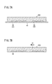
一般に、ドハティ増幅器は、キャリア増幅器12及びピーク増幅器14で増幅された高周波電力が内部で合成されることから、発熱しやすい。そこで、誘電体基板42に上述の複数の溝90を形成することで、合成器10cで発生した熱を大気中に逃がしやすくなり、発熱による合成器10cの損失の増大を抑制することができ、しかも、合成器10cの許容入力を高めることができる。
In general, the Doherty amplifier is likely to generate heat because the high-frequency power amplified by the
第4変形例に係る合成器10dは、図38に示すように、誘電体基板42に形成された複数のサーマルビア92を有する。サーマルビア92の形成位置としては、例えば誘電体基板42の上面42eから上部シールド電極46a(図3参照)に達する領域、誘電体基板42の下面42fから下部シールド電極46b(図3参照及)に達する領域等がある。
The
この合成器10dにおいては、キャリア増幅器12とピーク増幅器14からの信号が入力されることによって、合成器10d内で発生した熱をサーマルビア92を通じて大気中や回路基板に逃がしやすくなり、発熱による合成器10dの損失の増大を抑制することができ、しかも、合成器10dの許容入力を高めることができる。
In the
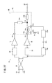
[第1実施例]
比較例1、実施例1〜実施例3について、それぞれの出力特性を確認した。[First embodiment]
The output characteristics of Comparative Example 1 and Examples 1 to 3 were confirmed.
(比較例1)
図39に示すように、信号分配器20、キャリア側インピーダンス整合部22、ピーク側インピーダンス整合部24、キャリア増幅器12及びピーク増幅器14を有する通常のドハティ増幅器16の出力に、比較例1に係る合成器200を接続し、さらに、合成器200の出力に、特性インピーダンスが50オームのマイクロストリップ線路202(1cm)を介して30dBの方向性結合器204を接続した。すなわち、回路基板上に、ドハティ増幅器16と、比較例1に係る合成器200と、マイクロストリップ線路202と、方向性結合器204とを実装した。比較例1に係る合成器200は、誘電体基板42内に第1λ/4線路34Aと、合成点32と、第2λ/4線路34Bとを形成してチップ化した。(Comparative Example 1)
As shown in FIG. 39, the output of a
そして、出力端子30から出力される信号に基づいてドハティ増幅器16の利得及び増幅器効率の測定を行った。このとき、比較例1に係る合成器200からの出力は52.8dBmであった。
Based on the signal output from the
続いて、回路基板に実装されたものと同じ長さのマイクロストリップ線路202と30dBの方向性結合器204とを含む全体の挿入損失を測定したところ、0.16dBであった。
Subsequently, the entire insertion loss including the
従って、マイクロストリップ線路202と方向性結合器204による損失パワーは7.1Wと計算される。
Therefore, the loss power due to the
(実施例1)
回路基板上に、通常のドハティ増幅器16と、図23及び図24に示す第9合成器10Iとを実装し、第9合成器10Iのキャリア側入力端子26にキャリア増幅器12を接続し、ピーク側入力端子28にピーク増幅器14を接続した。(Example 1)
A
第3モニタ端子36cに接続された第3モニタ回路50cから出力される信号に基づいてドハティ増幅器16の利得及び増幅器効率の測定を行った。このとき、第9合成器10Iからの出力は52.9dBmであった。
Based on the signal output from the
合成器の部分と第3方向性結合器40Cの部分とが誘電体基板42内で一体化された第9合成器10Iによる損失パワーは3.9Wであり、比較例1に対して4.4Wの改善が実現できた。このときの増幅器効率は45%であったので、消費電力で9.8W改善された。これは、比較例1にて実装したマイクロストリップ線路202の配線ロスがなくなった上に、図24に示すように、第1λ/4線路34A、合成点32及び第2λ/4線路34Bとからなる合成器の部分と第3方向性結合器40Cとを内層シールド電極48を間に挟んで上下に重ねることで、接続配線長を最短にすることができたためと考えられる。
The loss power of the ninth combiner 10I in which the combiner portion and the third
(実施例2)
回路基板上に、通常のドハティ増幅器16と、図1〜図3に示す第1合成器10Aとを実装し、第1合成器10Aのキャリア側入力端子26にキャリア増幅器12を接続し、ピーク側入力端子28にピーク増幅器14を接続した。(Example 2)
A
第1モニタ端子36aに接続された第1モニタ回路50aから出力される信号に基づいてドハティ増幅器16の利得及び増幅器効率の測定を行った。このとき、第1合成器10Aからの出力は52.95dBであり、比較例1に対して6.7Wほど改善された。これは消費電力で14Wの改善となる。
Based on the signal output from the
比較例1に比べ、配線のマイクロストリップ線路202のロスがなくなったことに加え、追加の方向性結合器204による損失がなくなったことによる効果と考えられる。
Compared with Comparative Example 1, it is considered that the loss due to the additional
(実施例3)
回路基板上に、通常のドハティ増幅器16と、図14及び図15に示す第4合成器10Dとを実装し、第4合成器10Dのキャリア側入力端子26にキャリア増幅器12を接続し、ピーク側入力端子28にピーク増幅器14を接続した。(Example 3)
A
第2モニタ端子36bに接続された第2モニタ回路50bから出力される信号(高周波信号の包絡線)に基づいてキャリア増幅器12のゲートバイアスコントロールを行った。W−CDMA信号を用い、隣接チャンネル漏洩電力(ACLR Adjacent channel leakage ratio)を測定したところ、−45dBcから2dBcほど改善することができた。
The gate bias of the
[第2実施例]
比較例2、実施例11及び実施例12について、それぞれの出力特性を確認した。[Second Embodiment]
The output characteristics of Comparative Example 2, Example 11 and Example 12 were confirmed.
(比較例2)
図40に示すように、信号分配器20、キャリア側インピーダンス整合部22、ピーク側インピーダンス整合部24、キャリア増幅器12及びピーク増幅器14を有する通常のドハティ増幅器16の出力に、比較例2に係る合成器200を接続した。すなわち、回路基板上に、ドハティ増幅器16と、比較例2に係る合成器200とを実装した。比較例2に係る合成器200は、誘電体基板42内に第1λ/4線路34Aと、合成点32と、第2λ/4線路34Bとを形成してチップ化した。(Comparative Example 2)
As shown in FIG. 40, the output of a
そして、ドハティ増幅器16の基本特性である利得特性及び効率特性を計測したところ、図41のような特性であった。このドハティ増幅器16では、入力側の信号分配器20に3dBハイブリッドカプラを使用しているため、最大出力(利得が1dB低下する点)より約6dB低い出力において効率特性に変曲点Paが見られる。この変曲点paよりもさらに効率を上げようとすると、利得特性に変曲点Pbが現れる。
And when the gain characteristic and the efficiency characteristic which are the basic characteristics of the
なお、ドハティ増幅器16が取り扱う信号のピーク・アベレージ信号パワー比(PAPR:Peak Average Power Ratio)に応じて、入力側の信号分配器20の信号分配比は適宜選択可能であり、例えばPAPR=8dBの場合は、入力側の信号分配器20に5dBの不等分配カプラを使用することにより達成可能である。
Note that the signal distribution ratio of the
そして、ドハティ増幅器16に対して、歪補償器としてDPD(Digital Pre Distortion)を用いて歪補償前後での歪計測を実施した。入力信号はW−CDMAを用い、隣接チャネル漏洩電力(ACLR Adjacent Channel Leakage power Ratio)により歪を評価した。
The
比較例2では、歪補償前のACLRが−45dBcに対し、歪補償後のACLRは−50dBcとなり、歪補償による歪の改善は−5dBcに留まった。 In Comparative Example 2, the ACLR before distortion compensation was −45 dBc, whereas the ACLR after distortion compensation was −50 dBc, and the distortion improvement due to distortion compensation remained at −5 dBc.
(実施例11)
回路基板上に、通常のドハティ増幅器16と、図25及び図26に示す第10合成器10Jとを実装し、第10合成器10Jのキャリア側入力端子26にキャリア増幅器12を接続し、ピーク側入力端子28にピーク増幅器14を接続した。そして、第4モニタ端子36dに接続された第4モニタ回路50dからの出力を、キャリア増幅器12のゲートバイアス電圧を制御するための第1制御器74aに入力し、キャリア増幅器12からのキャリア信号の振幅レベルに基づいてキャリア増幅器12のゲートバイアス電圧を制御可能とした。(Example 11)
A
これにより、キャリア増幅器12の利得が低下し始める出力領域において、ゲートバイアス電圧を上げることで、キャリア増幅器12の利得低減を抑制できることから、図42に示すように、従来のドハティ増幅器16の利得に見られた変曲点Pb(図41及び図45参照)の発生を抑制することが可能となり、この結果、DPDによる歪補償が容易となる。
Thereby, in the output region where the gain of the
例えば比較例2と同等の計測条件において、歪を計測したところ、歪補償前のACLRが−45dBcだったのに対し、歪補償後のACLRは−56dBcとなり、比較例2と比較して歪の改善度合いが−6dBc向上した。 For example, when distortion was measured under the same measurement conditions as in Comparative Example 2, the ACLR before distortion compensation was −45 dBc, whereas the ACLR after distortion compensation was −56 dBc, which was higher than that in Comparative Example 2. The improvement degree was improved by -6 dBc.
(実施例12)
回路基板上に、通常のドハティ増幅器16と、図29及び図30に示す第12合成器10Lとを実装し、第12合成器10Lのキャリア側入力端子26にキャリア増幅器12を接続し、ピーク側入力端子28にピーク増幅器14を接続した。そして、第4モニタ端子36dに接続された第4モニタ回路50dからの出力を、キャリア増幅器12のゲートバイアス電圧を制御するための第1制御器74aに入力し、さらに、第5モニタ端子36eに接続された第5モニタ回路50eからの出力を、ピーク増幅器14のゲートバイアス電圧を制御するための第2制御器74bに入力し、キャリア増幅器12からのキャリア信号の振幅レベルに基づいてキャリア増幅器12のゲートバイアス電圧を制御可能とすると共に、ピーク増幅器14からのピーク信号の振幅レベルに基づいてピーク増幅器14のゲートバイアス電圧を制御可能とした。(Example 12)
A
これにより、キャリア増幅器12の利得低減抑制効果に加え、ピーク増幅器14の利得低減も抑制できることから、図43に示すように、この実施例12では、実施例11と比較して高出力領域での利得低減がさらに抑制される。この結果、DPDによる歪補償がさらに容易となる。
Thereby, in addition to the gain reduction suppressing effect of the
例えば比較例2と同等の計測条件において、歪を計測したところ、歪補償前のACLRが−48dBcだったのに対し、歪補償後のACLRは−61dBcとなり、比較例2と比較して歪の改善度合いが−8dBc改善した。 For example, when distortion was measured under the same measurement conditions as in Comparative Example 2, the ACLR before distortion compensation was −48 dBc, whereas the ACLR after distortion compensation was −61 dBc. The degree of improvement was improved by -8 dBc.
なお、本発明に係るドハティ増幅器用合成器は、上述の実施の形態に限らず、本発明の要旨を逸脱することなく、種々の構成を採り得ることはもちろんである。 It should be noted that the Doherty amplifier combiner according to the present invention is not limited to the above-described embodiment, but can of course have various configurations without departing from the gist of the present invention.
Claims (19)
前記キャリア増幅器(12)からの出力が入力される第1入力端子(26)と、
前記ピーク増幅器(14)からの出力が入力される第2入力端子(28)と、
前記キャリア増幅器(12)からの出力と前記ピーク増幅器(14)からの出力とを合成した信号が出力される出力端子(30)と、
前記キャリア増幅器(12)からの出力と前記ピーク増幅器(14)からの出力との合成点(32)と、
前記第1入力端子(26)と前記合成点(32)との間に接続された第1λ/4線路(34A)と、
前記合成点(32)と前記出力端子(30)との間に接続された第2λ/4線路(34B)と、
前記第1入力端子(26)から前記合成点(32)にかけて流れる信号、前記第2入力端子(28)から前記合成点(32)にかけて流れる信号及び前記合成点(32)から前記出力端子(30)にかけて流れる信号のうち、1以上の信号をモニタする信号モニタ手段とを有し、
前記信号モニタ手段は、方向性結合器(40A又は40B)を備え、
前記方向性結合器(40A又は40B)は、
前記第1λ/4線路(34A)及び前記第2λ/4線路(34B)のうち、モニタ対象のλ/4線路と電磁結合する第3λ/4線路(34C)を有し、
複数の誘電体層が積層されて構成された誘電体基板(42)を有し、
前記第1入力端子(26)、前記第2入力端子(28)及び前記出力端子(30)が前記誘電体基板(42)の表面に形成され、
前記第1λ/4線路(34A)、前記第2λ/4線路(34B)及び前記第3λ/4線路(34C)が前記誘電体基板(42)内に形成され、
前記誘電体基板(42)内に、前記第1λ/4線路(34A)及び前記第2λ/4線路(34B)のうち、前記モニタ対象のλ/4線路、並びに前記第3λ/4線路(34C)と、前記第1λ/4線路(34A)及び前記第2λ/4線路(34B)のうち、前記モニタ対象外のλ/4線路との間に形成された内層シールド電極(48)を有することを特徴とするドハティ増幅器用合成器。 A Doherty amplifier connected to the output of a Doherty amplifier (16) having a carrier amplifier (12) and a peak amplifier (14) and combining the output from the carrier amplifier (12) and the output from the peak amplifier (14). A synthesizer for
A first input terminal (26) to which an output from the carrier amplifier (12) is input;
A second input terminal (28) to which an output from the peak amplifier (14) is input;
An output terminal (30) for outputting a signal obtained by combining the output from the carrier amplifier (12) and the output from the peak amplifier (14);
A combining point (32) of the output from the carrier amplifier (12) and the output from the peak amplifier (14);
A first λ / 4 line (34A) connected between the first input terminal (26) and the combining point (32);
A second λ / 4 line (34B) connected between the composite point (32) and the output terminal (30);
A signal that flows from the first input terminal (26) to the synthesis point (32), a signal that flows from the second input terminal (28) to the synthesis point (32), and a signal that flows from the synthesis point (32) to the output terminal (30) ) toward among the signals flowing, it has a signal monitoring means for monitoring one or more signals,
The signal monitoring means includes a directional coupler (40A or 40B),
The directional coupler (40A or 40B) is
Of the first λ / 4 line (34A) and the second λ / 4 line (34B), a third λ / 4 line (34C) that is electromagnetically coupled to the λ / 4 line to be monitored is provided.
A dielectric substrate (42) configured by laminating a plurality of dielectric layers;
The first input terminal (26), the second input terminal (28) and the output terminal (30) are formed on a surface of the dielectric substrate (42);
The first λ / 4 line (34A), the second λ / 4 line (34B), and the third λ / 4 line (34C) are formed in the dielectric substrate (42),
Among the first λ / 4 line (34A) and the second λ / 4 line (34B) in the dielectric substrate (42), the λ / 4 line to be monitored and the third λ / 4 line (34C) ) And an inner layer shield electrode (48) formed between the first λ / 4 line (34A) and the second λ / 4 line (34B) and the λ / 4 line not to be monitored. A Doherty amplifier combiner.
前記第3λ/4線路(34C)の一端にモニタ端子(36a又は36b)が接続され、前記第3λ/4線路(34C)の他端に終端抵抗(Re)が接続され、
前記モニタ端子(36a又は36b)は前記誘電体基板(42)の表面に形成されていることを特徴とするドハティ増幅器用合成器。 The synthesizer for Doherty amplifier according to claim 1 ,
A monitor terminal (36a or 36b) is connected to one end of the third λ / 4 line (34C), and a termination resistor (Re) is connected to the other end of the third λ / 4 line (34C) ,
The Doherty amplifier synthesizer characterized in that the monitor terminal (36a or 36b) is formed on the surface of the dielectric substrate (42) .
前記キャリア増幅器(12)からの出力が入力される第1入力端子(26)と、
前記ピーク増幅器(14)からの出力が入力される第2入力端子(28)と、
前記キャリア増幅器(12)からの出力と前記ピーク増幅器(14)からの出力とを合成した信号が出力される出力端子(30)と、
前記キャリア増幅器(12)からの出力と前記ピーク増幅器(14)からの出力との合成点(32)と、
前記第1入力端子(26)と前記合成点(32)との間に接続された第1λ/4線路(34A)と、
前記合成点(32)と前記出力端子(30)との間に接続された第2λ/4線路(34B)と、
前記第1入力端子(26)から前記合成点(32)にかけて流れる信号、前記第2入力端子(28)から前記合成点(32)にかけて流れる信号及び前記合成点(32)から前記出力端子(30)にかけて流れる信号のうち、1以上の信号をモニタする信号モニタ手段とを有し、
前記信号モニタ手段は、方向性結合器(40A又は40B)を備え、
前記方向性結合器(40A又は40B)は、
前記第1λ/4線路(34A)及び前記第2λ/4線路(34B)のうち、モニタ対象のλ/4線路と電磁結合する第3λ/4線路(34C)を有し、
さらに、前記第3λ/4線路(34C)に接続され、且つ、該第3λ/4線路(34C)の特性インピーダンスを前記モニタ対象のλ/4線路の特性インピーダンスと整合させるための第4λ/4線路(34D)とを有し、
前記モニタ対象のλ/4線路、前記第3λ/4線路(34C)及び前記第4λ/4線路(34D)の各特性インピーダンスが共に同じであることを特徴とするドハティ増幅器用合成器。 A Doherty amplifier connected to the output of a Doherty amplifier (16) having a carrier amplifier (12) and a peak amplifier (14) and combining the output from the carrier amplifier (12) and the output from the peak amplifier (14). A synthesizer for
A first input terminal (26) to which an output from the carrier amplifier (12) is input;
A second input terminal (28) to which an output from the peak amplifier (14) is input;
An output terminal (30) for outputting a signal obtained by combining the output from the carrier amplifier (12) and the output from the peak amplifier (14);
A combining point (32) of the output from the carrier amplifier (12) and the output from the peak amplifier (14);
A first λ / 4 line (34A) connected between the first input terminal (26) and the combining point (32);
A second λ / 4 line (34B) connected between the composite point (32) and the output terminal (30);
A signal that flows from the first input terminal (26) to the synthesis point (32), a signal that flows from the second input terminal (28) to the synthesis point (32), and a signal that flows from the synthesis point (32) to the output terminal (30) Signal monitoring means for monitoring one or more of the signals flowing over
The signal monitoring means includes a directional coupler (40A or 40B),
The directional coupler (40A or 40B) is
Of the first λ / 4 line (34A) and the second λ / 4 line (34B), a third λ / 4 line (34C) that is electromagnetically coupled to the λ / 4 line to be monitored is provided.
Further, a fourth λ / 4 connected to the third λ / 4 line (34C) and for matching the characteristic impedance of the third λ / 4 line (34C) with the characteristic impedance of the λ / 4 line to be monitored. Line (34D),
The Doherty amplifier combiner characterized in that the characteristic impedances of the monitored λ / 4 line, the third λ / 4 line (34C), and the fourth λ / 4 line (34D) are all the same.
前記第3λ/4線路(34C)は、前記第2λ/4線路(34B)と電磁結合されていることを特徴とするドハティ増幅器用合成器。 The synthesizer for Doherty amplifier according to any one of claims 1 to 3 ,
The Doherty amplifier combiner, wherein the third λ / 4 line (34C) is electromagnetically coupled to the second λ / 4 line (34B).
前記第3λ/4線路(34C)は、前記第1λ/4線路(34A)と電磁結合されていることを特徴とするドハティ増幅器用合成器。 The synthesizer for Doherty amplifier according to any one of claims 1 to 3 ,
The Doherty amplifier combiner, wherein the third λ / 4 line (34C) is electromagnetically coupled to the first λ / 4 line (34A).
前記第3λ/4線路(34C)の一端に前記第4λ/4線路(34D)の一端が接続され、前記第3λ/4線路(34C)の他端に終端抵抗(Re)が接続され、
前記第4λ/4線路(34D)の他端にモニタ端子(36a又は36b)が接続されていることを特徴とするドハティ増幅器用合成器。 The synthesizer for Doherty amplifier according to claim 3 ,
One end of the fourth λ / 4 line (34D) is connected to one end of the third λ / 4 line (34C), and a termination resistor (Re) is connected to the other end of the third λ / 4 line (34C),
A Doherty amplifier synthesizer, characterized in that a monitor terminal (36a or 36b) is connected to the other end of the fourth λ / 4 line (34D).
前記第3λ/4線路(34C)の一端に前記第4λ/4線路(34D)の一端が接続され、前記第3λ/4線路(34C)の他端にモニタ端子(36a又は36b)が接続され、
前記第4λ/4線路(34D)の他端に終端抵抗(Re)が接続されていることを特徴とするドハティ増幅器用合成器。 The synthesizer for Doherty amplifier according to claim 3 ,
One end of the fourth λ / 4 line (34D) is connected to one end of the third λ / 4 line (34C), and a monitor terminal (36a or 36b) is connected to the other end of the third λ / 4 line (34C). ,
A Doherty amplifier synthesizer, characterized in that a terminating resistor (Re) is connected to the other end of the fourth λ / 4 line (34D).
複数の誘電体層が積層されて構成された誘電体基板(42)を有し、
前記第1入力端子(26)、前記第2入力端子(28)、前記出力端子(30)及び前記モニタ端子(36a又は36b)が前記誘電体基板(42)の表面に形成され、
前記第1λ/4線路(34A)、前記第2λ/4線路(34B)、前記第3λ/4線路(34C)及び前記第4λ/4線路(34D)が前記誘電体基板(42)内に形成されていることを特徴とするドハティ増幅器用合成器。 The synthesizer for Doherty amplifier according to claim 6 or 7 ,
A dielectric substrate (42) configured by laminating a plurality of dielectric layers;
The first input terminal (26), the second input terminal (28), the output terminal (30) and the monitor terminal (36a or 36b) are formed on the surface of the dielectric substrate (42),
The first λ / 4 line (34A), the second λ / 4 line (34B), the third λ / 4 line (34C), and the fourth λ / 4 line (34D) are formed in the dielectric substrate (42). A synthesizer for Doherty amplifiers.
前記誘電体基板(42)内に、前記第1λ/4線路(34A)及び前記第2λ/4線路(34B)のうち、前記モニタ対象のλ/4線路並びに前記第3λ/4線路(34C)と、前記第1λ/4線路(34A)及び前記第2λ/4線路(34B)のうち、前記モニタ対象外のλ/4線路との間に形成された第1内層シールド電極(48a)と、
前記誘電体基板(42)内に、前記モニタ対象のλ/4線路と、前記第4λ/4線路(34D)との間に形成された第2内層シールド電極(48b)とを有することを特徴とするドハティ増幅器用合成器。 The synthesizer for Doherty amplifier according to claim 8 ,
Of the first λ / 4 line (34A) and the second λ / 4 line (34B), the λ / 4 line to be monitored and the third λ / 4 line (34C) in the dielectric substrate (42). A first inner shield electrode (48a) formed between the first λ / 4 line (34A) and the second λ / 4 line (34B) and the λ / 4 line that is not monitored,
The dielectric substrate (42) has a second inner shield electrode (48b) formed between the λ / 4 line to be monitored and the fourth λ / 4 line (34D). A synthesizer for Doherty amplifier.
前記第3λ/4線路(34C)と前記第4λ/4線路(34D)とがビアホール(72)を介して接続されていることを特徴とするドハティ増幅器用合成器。 The Doherty amplifier combiner according to claim 8 or 9 ,
The Doherty amplifier combiner, wherein the third λ / 4 line (34C) and the fourth λ / 4 line (34D) are connected via a via hole (72).
前記モニタ端子(36a又は36b)に、前記方向性結合器(40A又は40B)の出力をモニタするためのモニタ回路(50a又は50b)が接続され、
前記モニタ回路(50a又は50b)は、ダイオード(Da)を有することを特徴とするドハティ増幅器用合成器。 The synthesizer for Doherty amplifier according to claim 2 or 6 ,
A monitor circuit (50a or 50b) for monitoring the output of the directional coupler (40A or 40B) is connected to the monitor terminal (36a or 36b),
The monitor circuit (50a or 50b) includes a diode (Da), and a Doherty amplifier combiner.
前記キャリア増幅器(12)からの出力が入力される第1入力端子(26)と、
前記ピーク増幅器(14)からの出力が入力される第2入力端子(28)と、
前記キャリア増幅器(12)からの出力と前記ピーク増幅器(14)からの出力とを合成した信号が出力される出力端子(30)と、
前記キャリア増幅器(12)からの出力と前記ピーク増幅器(14)からの出力との合成点(32)と、
前記第1入力端子(26)と前記合成点(32)との間に接続された第1λ/4線路(34A)と、
前記合成点(32)と前記出力端子(30)との間に接続された第2λ/4線路(34B)と、
前記第1入力端子(26)から前記合成点(32)にかけて流れる信号、前記第2入力端子(28)から前記合成点(32)にかけて流れる信号及び前記合成点(32)から前記出力端子(30)にかけて流れる信号のうち、1以上の信号をモニタする信号モニタ手段とを有し、
前記信号モニタ手段は、方向性結合器(40C)を備え、
前記方向性結合器(40C)は、
前記第2λ/4線路(34B)と前記出力端子(30)との間に接続された第5λ/4線路(34E)と、
前記第5λ/4線路(34E)と電磁結合する第6λ/4線路(34F)とを有し、
複数の誘電体層が積層されて構成された誘電体基板(42)を有し、
前記第1入力端子(26)、前記第2入力端子(28)及び前記出力端子(30)が前記誘電体基板(42)の表面に形成され、
前記第1λ/4線路(34A)、前記第2λ/4線路(34B)、前記第5λ/4線路(34E)及び前記第6λ/4線路(34F)が前記誘電体基板(42)内に形成され、
前記誘電体基板(42)内に、前記第1λ/4線路(34A)及び前記第2λ/4線路(34B)と、前記第5λ/4線路(34E)及び前記第6λ/4線路(34F)との間に形成された内層シールド電極(48)を有することを特徴とするドハティ増幅器用合成器。 A Doherty amplifier connected to the output of a Doherty amplifier (16) having a carrier amplifier (12) and a peak amplifier (14) and combining the output from the carrier amplifier (12) and the output from the peak amplifier (14). A synthesizer for
A first input terminal (26) to which an output from the carrier amplifier (12) is input;
A second input terminal (28) to which an output from the peak amplifier (14) is input;
An output terminal (30) for outputting a signal obtained by combining the output from the carrier amplifier (12) and the output from the peak amplifier (14);
A combining point (32) of the output from the carrier amplifier (12) and the output from the peak amplifier (14);
A first λ / 4 line (34A) connected between the first input terminal (26) and the combining point (32);
A second λ / 4 line (34B) connected between the composite point (32) and the output terminal (30);
A signal that flows from the first input terminal (26) to the synthesis point (32), a signal that flows from the second input terminal (28) to the synthesis point (32), and a signal that flows from the synthesis point (32) to the output terminal (30) Signal monitoring means for monitoring one or more of the signals flowing over
The signal monitoring means includes a directional coupler (40C),
The directional coupler (40C)
A fifth λ / 4 line (34E) connected between the second λ / 4 line (34B) and the output terminal (30);
A sixth λ / 4 line (34F) electromagnetically coupled to the fifth λ / 4 line (34E);
A dielectric substrate (42) configured by laminating a plurality of dielectric layers;
The first input terminal (26), the second input terminal (28) and the output terminal (30) are formed on a surface of the dielectric substrate (42);
The first λ / 4 line (34A), the second λ / 4 line (34B), the fifth λ / 4 line (34E), and the sixth λ / 4 line (34F) are formed in the dielectric substrate (42). And
In the dielectric substrate (42), the first λ / 4 line (34A) and the second λ / 4 line (34B), the fifth λ / 4 line (34E) and the sixth λ / 4 line (34F). And an inner layer shield electrode (48) formed therebetween.
前記第6λ/4線路(34F)の一端にモニタ端子(36c)が接続され、前記第6λ/4線路(34F)の他端に終端抵抗(Re)が接続され、
前記モニタ端子(36c)は前記誘電体基板(42)の表面に形成されていることを特徴とするドハティ増幅器用合成器。 The synthesizer for Doherty amplifier according to claim 12 ,
A monitor terminal (36c) is connected to one end of the sixth λ / 4 line (34F), and a termination resistor (Re) is connected to the other end of the sixth λ / 4 line (34F) .
The Doherty amplifier combiner, wherein the monitor terminal (36c) is formed on a surface of the dielectric substrate (42) .
前記第1入力端子(26)と前記第1λ/4線路(34A)とが容量結合され、
前記第2入力端子(28)と前記第2λ/4線路(34B)とが容量結合されていることを特徴とするドハティ増幅器用合成器。 The synthesizer for Doherty amplifier according to any one of claims 1 to 13 ,
The first input terminal (26) and the first λ / 4 line (34A) are capacitively coupled,
The Doherty amplifier combiner, wherein the second input terminal (28) and the second λ / 4 line (34 B ) are capacitively coupled.
前記複数のキャリア増幅器(12)からの出力が入力される複数の第1入力端子(26)と、
前記ピーク増幅器(14)からの出力が入力される1つの第2入力端子(28)と、
前記複数のキャリア増幅器(12)からの各出力と前記ピーク増幅器(14)からの出力とを合成した信号が出力される1つの出力端子(30)と、
前記複数のキャリア増幅器(12)からの出力と前記ピーク増幅器(14)からの出力との合成点(32)と、
前記複数の第1入力端子(26)と前記合成点(32)との間にそれぞれ接続された複数の第1λ/4線路(34A)と、
前記合成点(32)と前記出力端子(30)との間に接続された第2λ/4線路(34B)と、
前記複数の第1入力端子(26)から前記合成点(32)にかけてそれぞれ流れる信号、前記第2入力端子(28)から前記合成点(32)にかけて流れる信号及び前記合成点(32)から前記出力端子(30)にかけて流れる信号のうち、1以上の信号をモニタする信号モニタ手段とを有し、
複数の誘電体層が積層されて構成された誘電体基板(42)を有し、
前記複数の第1入力端子(26)、前記第2入力端子(28)及び前記出力端子(30)が前記誘電体基板(42)の表面に形成され、
前記複数の第1λ/4線路(34A)及び前記第2λ/4線路(34B)が前記誘電体基板(42)内に形成され、
前記誘電体基板(42)内のうち、前記複数の第1λ/4線路(34A)間、並びに、前記複数の第1λ/4線路(34A)と前記第2λ/4線路(34B)間にそれぞれ内層シールド電極(48)が形成されていることを特徴とするドハティ増幅器用合成器。 Connected to the output of a Doherty amplifier (16) having a plurality of carrier amplifiers (12) and a peak amplifier (14), each output from the plurality of carrier amplifiers (12) and from the peak amplifier (14) A synthesizer for Doherty amplifier that synthesizes the output,
A plurality of first input terminals (26) to which outputs from the plurality of carrier amplifiers (12) are input;
One second input terminal (28) to which the output from the peak amplifier (14) is input;
One output terminal (30) from which a signal obtained by combining the outputs from the plurality of carrier amplifiers (12) and the output from the peak amplifier (14) is output;
A combining point (32) of the outputs from the plurality of carrier amplifiers (12) and the output from the peak amplifier (14);
A plurality of first λ / 4 lines (34A) respectively connected between the plurality of first input terminals (26) and the composite point (32);
A second λ / 4 line (34B) connected between the composite point (32) and the output terminal (30);
Signals flowing from the plurality of first input terminals (26) to the synthesis point (32), signals flowing from the second input terminal (28) to the synthesis point (32), and output from the synthesis point (32) among the signals flowing over the pin (30), have a signal monitoring means for monitoring one or more signals,
A dielectric substrate (42) configured by laminating a plurality of dielectric layers;
The plurality of first input terminals (26), the second input terminals (28), and the output terminals (30) are formed on a surface of the dielectric substrate (42),
The plurality of first λ / 4 lines (34A) and the second λ / 4 line (34B) are formed in the dielectric substrate (42),
Within the dielectric substrate (42), between the plurality of first λ / 4 lines (34A) and between the plurality of first λ / 4 lines (34A) and the second λ / 4 lines (34B). combiner for Doherty amplifier, wherein Rukoto has inner-layer shield electrode (48) is formed.
前記信号モニタ手段は、
前記キャリア増幅器(12)からのキャリア信号の振幅情報を出力するための第1モニタ端子(36d)を有することを特徴とするドハティ増幅器用合成器。 The synthesizer for Doherty amplifier according to claim 15 ,
The signal monitoring means includes
A Doherty amplifier combiner comprising a first monitor terminal (36d) for outputting amplitude information of a carrier signal from the carrier amplifier (12).
前記信号モニタ手段は、
前記第1入力端子(26)と前記第1λ/4線路(34A)との間の第1線路(76a)に平行して配置され、前記第1線路(76a)と電磁気的に結合された第1モニタ線路(78a)を有し、
前記第1モニタ線路(78a)は前記第1モニタ端子(36d)に接続されていることを特徴とするドハティ増幅器用合成器。 The synthesizer for Doherty amplifier according to claim 16 ,
The signal monitoring means includes
A first line (76a) between the first input terminal (26) and the first λ / 4 line (34A) is disposed in parallel, and is electromagnetically coupled to the first line (76a). 1 monitor line (78a)
The Doherty amplifier combiner, wherein the first monitor line (78a) is connected to the first monitor terminal (36d).
前記誘電体基板(42)のうち、回路基板が設置される面の反対面に設けられた複数の溝(90)を有することを特徴とするドハティ増幅器用合成器。 The synthesizer for Doherty amplifier according to claim 1, 12 or 15 ,
A Doherty amplifier combiner comprising a plurality of grooves (90) provided on a surface of the dielectric substrate (42) opposite to a surface on which a circuit board is placed.
前記誘電体基板(42)にサーマルビア(92)が形成されていることを特徴とするドハティ増幅器用合成器。 The synthesizer for Doherty amplifier according to claim 1, 12 or 15 ,
The Doherty amplifier synthesizer, wherein a thermal via (92) is formed in the dielectric substrate (42).
Applications Claiming Priority (5)
| Application Number | Priority Date | Filing Date | Title |
|---|---|---|---|
| US25433609P | 2009-10-23 | 2009-10-23 | |
| US25434309P | 2009-10-23 | 2009-10-23 | |
| US61/254343 | 2009-10-23 | ||
| US61/254336 | 2009-10-23 | ||
| PCT/JP2010/065958 WO2011048893A1 (en) | 2009-10-23 | 2010-09-15 | Combiner for doherty amplifier |
Publications (2)
| Publication Number | Publication Date |
|---|---|
| JPWO2011048893A1 JPWO2011048893A1 (en) | 2013-03-07 |
| JP5705122B2 true JP5705122B2 (en) | 2015-04-22 |
Family
ID=43900133
Family Applications (1)
| Application Number | Title | Priority Date | Filing Date |
|---|---|---|---|
| JP2011537180A Expired - Fee Related JP5705122B2 (en) | 2009-10-23 | 2010-09-15 | Doherty amplifier synthesizer |
Country Status (4)
| Country | Link |
|---|---|
| US (1) | US8847681B2 (en) |
| JP (1) | JP5705122B2 (en) |
| CN (1) | CN102577104B (en) |
| WO (1) | WO2011048893A1 (en) |
Families Citing this family (41)
| Publication number | Priority date | Publication date | Assignee | Title |
|---|---|---|---|---|
| EP2339745A1 (en) * | 2009-12-15 | 2011-06-29 | Nxp B.V. | Doherty amplifier |
| US8169277B2 (en) * | 2010-02-19 | 2012-05-01 | Harris Corporation | Radio frequency directional coupler device and related methods |
| DE102011075312A1 (en) | 2011-05-05 | 2012-11-08 | Rohde & Schwarz Gmbh & Co. Kg | Quasi-broadband Doherty amplifier and related capacitor circuit |
| US9306502B2 (en) | 2011-05-09 | 2016-04-05 | Qualcomm Incorporated | System providing switchable impedance transformer matching for power amplifiers |
| WO2011127868A2 (en) * | 2011-05-30 | 2011-10-20 | 华为技术有限公司 | Doherty power amplifier and signal processing method |
| JP2014518495A (en) | 2011-07-11 | 2014-07-28 | ロックスター コンソーティアム ユーエス エルピー | Amplifier linearization using non-standard feedback |
| KR20140053089A (en) * | 2011-07-13 | 2014-05-07 | 록스타 컨소시엄 유에스 엘피 | Broadband doherty amplifier using broadband transformer |
| US9007142B1 (en) | 2011-08-02 | 2015-04-14 | Anadigics, Inc. | Integrated output combiner for amplifier system |
| US8649744B2 (en) * | 2011-09-08 | 2014-02-11 | Alcatel Lucent | Radio-frequency transmitter, such as for broadcasting and cellular base stations |
| US8798561B2 (en) * | 2011-09-08 | 2014-08-05 | Alcatel Lucent | Radio-frequency circuit having a transcoupling element |
| US9071211B1 (en) * | 2011-12-15 | 2015-06-30 | Anadigics, Inc. | Compact doherty combiner |
| US8717099B2 (en) | 2012-03-16 | 2014-05-06 | Infineon Technologies Ag | Wideband doherty amplifier circuit with peaking impedance absorption |
| US8970297B2 (en) | 2012-03-19 | 2015-03-03 | Qualcomm Incorporated | Reconfigurable input power distribution doherty amplifier with improved efficiency |
| US9031518B2 (en) | 2012-12-17 | 2015-05-12 | Qualcomm Incorporated | Concurrent hybrid matching network |
| JP5786902B2 (en) * | 2013-06-26 | 2015-09-30 | 株式会社村田製作所 | Directional coupler |
| US9112458B2 (en) * | 2013-10-01 | 2015-08-18 | Telefonaktiebolaget L M Ericsson (Publ) | Wideband Doherty amplifier |
| US9537198B2 (en) | 2013-10-01 | 2017-01-03 | Telefonaktiebolaget L M Ericsson (Publ) | Wideband impedance transformer |
| WO2015106422A1 (en) * | 2014-01-16 | 2015-07-23 | Telefonaktiebolaget L M Ericsson (Publ) | Method and apparatus for adjusting peak power capability |
| US9595927B2 (en) * | 2014-08-18 | 2017-03-14 | Cree, Inc. | Bias adjustment circuitry for balanced amplifiers |
| US9503030B2 (en) * | 2014-10-17 | 2016-11-22 | Freescale Semiconductor, Inc. | Radio frequency power amplifier |
| CN104349448A (en) * | 2014-11-10 | 2015-02-11 | 天津天慧通科技有限公司 | Mobile phone signal micro-amplifier |
| JP2016100797A (en) * | 2014-11-25 | 2016-05-30 | 京セラ株式会社 | Filter integrated coupler and communication module |
| US9806681B2 (en) * | 2015-02-15 | 2017-10-31 | Skyworks Solutions, Inc. | Doherty power amplifier having AM-AM compensation |
| CN106206945A (en) | 2016-09-08 | 2016-12-07 | 京东方科技集团股份有限公司 | A kind of flexible base board and preparation method thereof, flexible display apparatus |
| US11374184B2 (en) | 2016-09-08 | 2022-06-28 | Boe Technology Group Co., Ltd. | Flexible substrate and fabrication method thereof, and flexible display apparatus |
| US11233483B2 (en) | 2017-02-02 | 2022-01-25 | Macom Technology Solutions Holdings, Inc. | 90-degree lumped and distributed Doherty impedance inverter |
| WO2018197918A1 (en) | 2017-04-24 | 2018-11-01 | Macom Technology Solutions Holdings, Inc. | Improved efficiency, symmetrical doherty power amplifier |
| CN110785928B (en) | 2017-04-24 | 2023-12-05 | 麦克姆技术解决方案控股有限公司 | Reverse doherty power amplifier with large RF fraction and instantaneous bandwidth |
| WO2019051709A1 (en) * | 2017-09-14 | 2019-03-21 | Telefonaktiebolaget Lm Ericsson (Publ) | Directional coupler and method for manufacturing the same as well as radio transmitter and radio device |
| US11283410B2 (en) | 2017-10-02 | 2022-03-22 | Macom Technology Solutions Holdings, Inc. | No-load-modulation, high-efficiency power amplifier |
| EP3474443B1 (en) | 2017-10-18 | 2021-03-10 | NXP USA, Inc. | Amplifier power combiner with slotline impedance transformer |
| US10554177B2 (en) * | 2017-11-27 | 2020-02-04 | Skyworks Solutions, Inc. | Quadrature combined doherty amplifiers |
| WO2019103899A1 (en) | 2017-11-27 | 2019-05-31 | Skyworks Solutions, Inc. | Wideband power combiner and splitter |
| KR102463954B1 (en) * | 2018-01-22 | 2022-11-04 | 미쓰비시덴키 가부시키가이샤 | amplifier |
| US10630241B2 (en) | 2018-08-23 | 2020-04-21 | Nxp Usa, Inc. | Amplifier with integrated directional coupler |
| JP7206754B2 (en) * | 2018-09-27 | 2023-01-18 | 富士通株式会社 | AMPLIFIER, WIRELESS COMMUNICATION DEVICE, AND METHOD OF CONTROLLING AMPLIFIER |
| CN112640298A (en) | 2018-10-05 | 2021-04-09 | 镁可微波技术有限公司 | Low load modulation power amplifier |
| US11094507B2 (en) | 2019-07-22 | 2021-08-17 | Tokyo Electron Limited | Power generation systems and methods for plasma stability and control |
| US11888448B2 (en) | 2019-12-30 | 2024-01-30 | Macom Technology Solutions Holdings, Inc. | Low-load-modulation broadband amplifier |
| US11770107B2 (en) * | 2021-01-19 | 2023-09-26 | Qualcomm Incorporated | Load-adaptive power amplifier |
| WO2022176947A1 (en) * | 2021-02-18 | 2022-08-25 | ヌヴォトンテクノロジージャパン株式会社 | High frequency power amplification device |
Citations (16)
| Publication number | Priority date | Publication date | Assignee | Title |
|---|---|---|---|---|
| JPH06216680A (en) * | 1993-01-18 | 1994-08-05 | Hitachi Ltd | Amplifier |
| JPH07106898A (en) * | 1993-10-04 | 1995-04-21 | Tdk Corp | High frequency signal distributer combiner |
| JP2002124840A (en) * | 2000-10-13 | 2002-04-26 | Mitsubishi Electric Corp | Doherty amplifier |
| JP2005525727A (en) * | 2002-01-28 | 2005-08-25 | クリー マイクロウエイブ インコーポレイテッド | N-way power amplifier with increased back-off power and power added efficiency |
| JP2006174409A (en) * | 2005-08-30 | 2006-06-29 | Toshiba Corp | Doherty high efficient amplifier for high frequency and signal processing method thereof |
| JP2006173722A (en) * | 2004-12-13 | 2006-06-29 | Toshiba Corp | Doherty high efficient amplifier for high frequency and signal processing method thereof |
| JP2006525751A (en) * | 2003-05-05 | 2006-11-09 | クリー マイクロウエイブ リミテッド ライアビリティ カンパニー | N-way RF power amplifier circuit with increased backoff capability and power added efficiency using selected phase length and output impedance |
| JP2007173647A (en) * | 2005-12-22 | 2007-07-05 | Matsushita Electric Works Ltd | Electromagnetic induction component and power supply apparatus |
| JP2007228062A (en) * | 2006-02-21 | 2007-09-06 | Toshiba Corp | Doherty amplifier |
| JP2008022513A (en) * | 2006-06-15 | 2008-01-31 | Hitachi Kokusai Electric Inc | Amplifier with distortion control function |
| JP2008219175A (en) * | 2007-02-28 | 2008-09-18 | Furuno Electric Co Ltd | Power synthesizing/distributing device and multi-point power feed circularly polarized wave antenna |
| WO2008123438A1 (en) * | 2007-03-29 | 2008-10-16 | Soshin Electric Co., Ltd. | Synthesizer for doherty amplifier |
| JP2009176839A (en) * | 2008-01-22 | 2009-08-06 | Mitsubishi Electric Corp | Heat dissipation structure of semiconductor element |
| JP2009206675A (en) * | 2008-02-27 | 2009-09-10 | Nec Corp | Power amplifier |
| JPWO2008136080A1 (en) * | 2007-04-20 | 2010-07-29 | 富士通株式会社 | Amplifying device and method for controlling Doherty amplifier circuit |
| JP2010206351A (en) * | 2009-03-02 | 2010-09-16 | Hitachi Kokusai Electric Inc | Power detector |
Family Cites Families (10)
| Publication number | Priority date | Publication date | Assignee | Title |
|---|---|---|---|---|
| US5966059A (en) * | 1997-09-02 | 1999-10-12 | Motorola, Inc. | Phase shifting power coupler with three signals of equal amplitude |
| US5886575A (en) * | 1997-09-30 | 1999-03-23 | Motorola, Inc. | Apparatus and method for amplifying a signal |
| JP2001060802A (en) * | 1999-08-19 | 2001-03-06 | Sony Corp | Circuit element substrate, semiconductor device and its manufacture |
| JP2004064377A (en) * | 2002-07-29 | 2004-02-26 | Hitachi Kokusai Electric Inc | Feedforward amplifier |
| US6825738B2 (en) * | 2002-12-18 | 2004-11-30 | Analog Devices, Inc. | Reduced size microwave directional coupler |
| CN101164229B (en) * | 2003-10-21 | 2010-12-08 | 安华高科技无线Ip(新加坡)私人有限公司 | High linearity doherty communication amplifier with bias control |
| CN100466373C (en) * | 2004-02-06 | 2009-03-04 | 株式会社村田制作所 | Balanced distributor |
| JP4715994B2 (en) * | 2004-08-26 | 2011-07-06 | 日本電気株式会社 | Doherty amplifier parallel operation circuit |
| US7446626B2 (en) * | 2006-09-08 | 2008-11-04 | Stmicroelectronics Ltd. | Directional couplers for RF power detection |
| US7671699B2 (en) * | 2007-08-14 | 2010-03-02 | Pine Valley Investments, Inc. | Coupler |
-
2010
- 2010-09-15 WO PCT/JP2010/065958 patent/WO2011048893A1/en active Application Filing
- 2010-09-15 CN CN201080047831.4A patent/CN102577104B/en not_active Expired - Fee Related
- 2010-09-15 JP JP2011537180A patent/JP5705122B2/en not_active Expired - Fee Related
- 2010-10-21 US US12/909,226 patent/US8847681B2/en not_active Expired - Fee Related
Patent Citations (16)
| Publication number | Priority date | Publication date | Assignee | Title |
|---|---|---|---|---|
| JPH06216680A (en) * | 1993-01-18 | 1994-08-05 | Hitachi Ltd | Amplifier |
| JPH07106898A (en) * | 1993-10-04 | 1995-04-21 | Tdk Corp | High frequency signal distributer combiner |
| JP2002124840A (en) * | 2000-10-13 | 2002-04-26 | Mitsubishi Electric Corp | Doherty amplifier |
| JP2005525727A (en) * | 2002-01-28 | 2005-08-25 | クリー マイクロウエイブ インコーポレイテッド | N-way power amplifier with increased back-off power and power added efficiency |
| JP2006525751A (en) * | 2003-05-05 | 2006-11-09 | クリー マイクロウエイブ リミテッド ライアビリティ カンパニー | N-way RF power amplifier circuit with increased backoff capability and power added efficiency using selected phase length and output impedance |
| JP2006173722A (en) * | 2004-12-13 | 2006-06-29 | Toshiba Corp | Doherty high efficient amplifier for high frequency and signal processing method thereof |
| JP2006174409A (en) * | 2005-08-30 | 2006-06-29 | Toshiba Corp | Doherty high efficient amplifier for high frequency and signal processing method thereof |
| JP2007173647A (en) * | 2005-12-22 | 2007-07-05 | Matsushita Electric Works Ltd | Electromagnetic induction component and power supply apparatus |
| JP2007228062A (en) * | 2006-02-21 | 2007-09-06 | Toshiba Corp | Doherty amplifier |
| JP2008022513A (en) * | 2006-06-15 | 2008-01-31 | Hitachi Kokusai Electric Inc | Amplifier with distortion control function |
| JP2008219175A (en) * | 2007-02-28 | 2008-09-18 | Furuno Electric Co Ltd | Power synthesizing/distributing device and multi-point power feed circularly polarized wave antenna |
| WO2008123438A1 (en) * | 2007-03-29 | 2008-10-16 | Soshin Electric Co., Ltd. | Synthesizer for doherty amplifier |
| JPWO2008136080A1 (en) * | 2007-04-20 | 2010-07-29 | 富士通株式会社 | Amplifying device and method for controlling Doherty amplifier circuit |
| JP2009176839A (en) * | 2008-01-22 | 2009-08-06 | Mitsubishi Electric Corp | Heat dissipation structure of semiconductor element |
| JP2009206675A (en) * | 2008-02-27 | 2009-09-10 | Nec Corp | Power amplifier |
| JP2010206351A (en) * | 2009-03-02 | 2010-09-16 | Hitachi Kokusai Electric Inc | Power detector |
Also Published As
| Publication number | Publication date |
|---|---|
| US8847681B2 (en) | 2014-09-30 |
| JPWO2011048893A1 (en) | 2013-03-07 |
| CN102577104A (en) | 2012-07-11 |
| US20110169590A1 (en) | 2011-07-14 |
| CN102577104B (en) | 2015-01-14 |
| WO2011048893A1 (en) | 2011-04-28 |
Similar Documents
| Publication | Publication Date | Title |
|---|---|---|
| JP5705122B2 (en) | Doherty amplifier synthesizer | |
| US7961064B2 (en) | Directional coupler including impedance matching and impedance transforming attenuator | |
| EP2732550A1 (en) | Broadband doherty amplifier using broadband transformer | |
| JP2004297456A (en) | High frequency module | |
| JP2005026368A (en) | Multilayer substrate with via hole for heat dissipation and power amplifier module using the same | |
| CN101728071B (en) | Transformer | |
| Shi et al. | A compact 65W 1.7–2.3 GHz class-E GaN power amplifier for base stations | |
| JP3729396B2 (en) | High frequency components | |
| CN107579325A (en) | A kind of LNA model filters power splitter | |
| JP4004333B2 (en) | Semiconductor module | |
| JP2003142981A5 (en) | ||
| JP2009241456A (en) | Dielectric substrate | |
| JP4711038B2 (en) | Non-reciprocal circuit module | |
| JPWO2005093948A1 (en) | amplifier | |
| KR101163777B1 (en) | Radio Frequency accumulated module and production method of circuit board of heat sink type for Radio Frequency accumulated module | |
| JP2001267466A (en) | Power amplifying module | |
| JP4479074B2 (en) | Manufacturing method and manufacturing apparatus for multilayer ceramic electronic component, multilayer ceramic electronic component, and ceramic green sheet | |
| CN218827834U (en) | Multi-frequency multi-layer integrated power division feed network | |
| CN114243238B (en) | LTCC filter capable of reducing layer thickness difference and preparation method thereof | |
| JP2011091801A (en) | Synthesizer for doherty amplifier | |
| CN107197598A (en) | A kind of preparation method of low PIM high performance microwaves high frequency composite ceramic substrate | |
| JP2001339260A (en) | Power amplifier module | |
| KR100381545B1 (en) | Laminated directional coupler | |
| US20040173879A1 (en) | High-frequency power amplifier | |
| JP2010239590A (en) | Distributed constant structural component, and method of manufacturing the same |
Legal Events
| Date | Code | Title | Description |
|---|---|---|---|
| A621 | Written request for application examination |
Free format text: JAPANESE INTERMEDIATE CODE: A621 Effective date: 20130808 |
|
| A131 | Notification of reasons for refusal |
Free format text: JAPANESE INTERMEDIATE CODE: A131 Effective date: 20140715 |
|
| A521 | Request for written amendment filed |
Free format text: JAPANESE INTERMEDIATE CODE: A523 Effective date: 20140910 |
|
| TRDD | Decision of grant or rejection written | ||
| A01 | Written decision to grant a patent or to grant a registration (utility model) |
Free format text: JAPANESE INTERMEDIATE CODE: A01 Effective date: 20150203 |
|
| A61 | First payment of annual fees (during grant procedure) |
Free format text: JAPANESE INTERMEDIATE CODE: A61 Effective date: 20150224 |
|
| R150 | Certificate of patent or registration of utility model |
Ref document number: 5705122 Country of ref document: JP Free format text: JAPANESE INTERMEDIATE CODE: R150 |
|
| LAPS | Cancellation because of no payment of annual fees |