US8245179B2 - RF circuit, circuit evaluation method, algorithm and recording medium - Google Patents
RF circuit, circuit evaluation method, algorithm and recording medium Download PDFInfo
- Publication number
- US8245179B2 US8245179B2 US12/312,551 US31255107A US8245179B2 US 8245179 B2 US8245179 B2 US 8245179B2 US 31255107 A US31255107 A US 31255107A US 8245179 B2 US8245179 B2 US 8245179B2
- Authority
- US
- United States
- Prior art keywords
- circuit
- port
- reflection coefficient
- amplifier
- product
- Prior art date
- Legal status (The legal status is an assumption and is not a legal conclusion. Google has not performed a legal analysis and makes no representation as to the accuracy of the status listed.)
- Expired - Fee Related, expires
Links
Images
Classifications
-
- G—PHYSICS
- G06—COMPUTING OR CALCULATING; COUNTING
- G06F—ELECTRIC DIGITAL DATA PROCESSING
- G06F30/00—Computer-aided design [CAD]
- G06F30/30—Circuit design
- G06F30/36—Circuit design at the analogue level
-
- G—PHYSICS
- G06—COMPUTING OR CALCULATING; COUNTING
- G06F—ELECTRIC DIGITAL DATA PROCESSING
- G06F30/00—Computer-aided design [CAD]
- G06F30/30—Circuit design
- G06F30/36—Circuit design at the analogue level
- G06F30/367—Design verification, e.g. using simulation, simulation program with integrated circuit emphasis [SPICE], direct methods or relaxation methods
Definitions
- the present invention relates to a technique for evaluating electric circuits such as an amplifier circuit and an oscillator circuit.
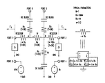
- Representative tools are the S-probe by Wang et al and the S-parameter Oscillator Test Component (equivalent to the S-probe in its actual circuit configuration) mounted as a standard item on the microwave circuit CAD software ADS of Agilent Technology ([1] K. Wang et al., “The S-Probe A New, Cost-Effective, 4-Gamma Method for Evaluating Multi-Stage Amplifier Stability”, 1992 MTT-S Digest, pp. 829-832).
- the S-probe is, as FIG. 1 shows, a 6-port circuit including large resistors (Rs,Rv) and voltage-dependent power sources M 3 and M 4 and is inserted, by use of ports 1 and 2 , in an arbitrary cross section of a circuit to be observed. Assume here that the ports 1 and 2 are connected respectively to Z 1 and Z 2 impedances. These impedances can be rendered from the passing characteristics from ports 5 and 6 to ports 3 and 4 .
- resistors Rs and Rv have quite a high resistance value, little current flows through the ports 6 , 5 , 4 , and 3 , which hardly affects the circuit Z 1 and Z 2 . Also, Rx connecting Z 1 and Z 2 in series to each other has quite a small value to lower insertion loss as much as possible.
- ⁇ S ( Z 1 ⁇ Z 0 )/( Z 1 +Z 0 )
- ⁇ L ( Z 2 ⁇ Z 0 )/( Z 2 +Z 0 ).
- Z 0 is system impedance and inner resistance of the S parameter probe and is ordinarily 50 ⁇ .
- Patent Document 1 Japanese Patent Laid-Open Publication No. 2001-177580
- the value of the probe resistance Rx is sufficiently small, e.g., 100 ⁇ as the typical value described above, the actual insertion loss can be substantially ignored.
- the reflection coefficients i.e., characteristic impedances
- the process to calculate the potential difference between both ends of the probe resistor is not adopted; hence, even if the probe resistance is quite small, there does not occur any problem in the numerical precision of the potential difference between both ends in the numeric calculation. Therefore, in a case wherein the reflection coefficients of a small signal of the circuit are obtained by the relevant S-probe, the S-probe can almost correctly calculate the reflection coefficients.
- the reflection coefficients of the circuit are obtained by the S-probe through a large-signal simulation, the reflection coefficients are calculated in an actual calculation based on an input signal to the circuit and a response thereto.
- the resistor Rx is employed as a voltage probe, if it is desired to lower the resistance value Rx to reduce the influence on the circuit, there takes place canceling of positions in the potential difference appearing on both ends of the resistor; there hence exists a problem that the resistance value Rx cannot be extremely reduced.
- the resistance Rx employed as a voltage probe is set, to lower the insertion loss, to a value remarkably smaller than the ordinary resistance component; hence, to obtain a probe voltage for high-precision observation, it is inevitable to input a relatively large probe signal; this causes perturbation in the circuit to be observed and leads to a situation wherein the reflection coefficients cannot be correctly obtained in the circuit.
- An exemplary object thereof is to provide an RF circuit, a circuit evaluation method, an algorithm, and a recording medium in which not only in a small-signal simulation but also in a large-signal simulation, loop oscillation and motorboating oscillation of an amplifier can be precisely predicted to quantitatively design a circuitry device to suppress oscillation without severing a loop or without inserting a circulator.
- the present invention has features as follows.
- a reflection coefficient measuring circuit (to be referred to as “no-loss S-probe” hereinbelow) proposed here is obtained by improving the S-probe by Wang et al; and by canceling the positive resistance component Rx by use of negative resistance, the probe is strictly a no-loss probe in circuit operation. Since the probe is a no-loss probe, it is not required to apply an extremely small value to the value of the probe resistance Rx. Therefore, to obtain reflection coefficients of a circuit in a large-signal state, the problem of the canceling of the potential difference at both ends of the probe resistor is removed; it is hence possible to obtain a probe voltage at high precision.
- the reflection coefficient calculation method employing the no-loss S-probe is capable of attaining reflection coefficients using an input of a sufficiently small probe signal which hardly causes perturbation in the circuit; it is also possible in a large-signal state and at an arbitrary point of the circuit to obtain coefficients (characteristic impedances) in consideration of a left-side section of the circuit and a right-side section thereof quite appropriately when compared with the relevant method.
- a first exemplary aspect of the present invention is an RF circuit on an actual circuit or a circuit simulator, including a function for being inserted by a first port and a second port thereof in a circuit to be observed, at an arbitrary cross-sectional point of the circuit, and evaluating a reflection coefficient or a characteristic impedance in the cross section, insertion loss between the first port and the second port strictly being completely zero.
- a second exemplary aspect of the present invention is a circuit on an actual circuit or a circuit simulator to be used in a microwave or millimeter wave range or a high-frequency range, including six RF ports, wherein a first resistor is connected from port 1 to a node a on the circuit, a second resistor is connected from the node a to a node b, a third resistor is connected from the node b to port 2 , a fourth resistor is connected from the node a to a node c, a fifth resistor is connected from the node b to a node d, and a sixth resistor is connected from the node b to a node e; a first DC block (or a capacitor which has quite a large capacity value and which passes therethrough an RF signal almost without loss) is connected from the node c to port 6 , a second DC block (or a capacitor which has quite a large capacity value and which passes therethrough an RF signal almost without loss) is connected from the
- the circuit in accordance with the second exemplary aspect may be a circuit wherein the first to sixth resistors are used at an environmental temperature of absolute zero degree (zero degree Kelvin) or the environmental temperature is set to absolute zero degree (zero degree Kelvin).
- a third exemplary aspect of the present invention is an evaluation method or an algorithm on a circuit simulator, wherein by inserting an RF circuit in accordance with the above exemplary aspects by the first port and the second port in a circuit to be observed, at an arbitrary cross-sectional point of the circuit and evaluating a forward or backward reflection coefficient (characteristic impedance); and by assuming that the forward reflection coefficient is ⁇ S and the backward reflection coefficient is ⁇ L , an absolute value of a product therebetween abs( ⁇ S ⁇ L ) is or the absolute value of the product and a phase angle of the product phase ( ⁇ S ⁇ L ) are employed as an index of stability of the circuit to be observed.
- a forward or backward reflection coefficient characteristic impedance
- a fourth exemplary aspect of the present invention also includes a measuring method and a measuring apparatus for electric circuits such as an amplifier circuit and an oscillator circuit, a designing method and a designing apparatus for the electric circuits, a recording medium having stored therein the measuring method of the electric circuits, and a recording medium having stored therein the designing method of the electric circuits, including the above exemplary aspects.
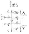
- the probe circuit of the present invention is a 6-port circuit including a voltage-dependent power source and resistors having a large resistance value, and the circuit is inserted by use of ports 1 and 2 as circuit insertion terminals in an arbitrary point of a circuit the reflection coefficients of which are to be obtained; referring to FIG. 2 , description will be given of perturbation caused in the circuit due to insertion of this probe in the circuit.
- the section between the ports 1 and 2 seems to be completely short-circuited (the resistance value is zero) because the resistance Rx is cancelled by ⁇ Rx obtained as the sum of the resistor values on both sides thereof, ⁇ Rx and ( ⁇ 1)RX.
- the resistor Rs since the resistor Rs has quite a large value, a current hardly flows through the ports 3 , 4 , 5 , and 6 and hence the circuit impedances Z 1 and Z 2 are not affected.
- a correct DC bias may also be applied.
- the resistor Rx to be inserted in series between the circuits Z 1 and Z 2 has a relatively small value, which is cancelled by the negative resistor ⁇ Rx additionally disposed; hence, the insertion loss of this probe can be strictly ignored.
- the resistor Rx operates as a voltage probe, but an extremely small value needs not to be employed for Rx; it is hence possible to prevent the canceling of the potential difference thereat in the numeric calculation.
- the noise temperature of each actual resistor to absolute zero degree (zero degree Kelvin)
- the influence exerted by this probe onto the noise factor NF of the circuit is completely zero (required in the design of LNA).
- the no-loss S-probe of the present invention is quite useful for the designing of a microwave circuit.
- the no-loss S-probe is an ideal probe to be used on a simulator and includes a voltage-dependent power source, capacitors, and resistors, and the probe is capable of obtaining reflection coefficients (forward and backward) at an insertion point with strictly zero insertion loss.
- the no-loss S-probe has in general a 6-port circuit configuration as shown in FIG. 2 and can be inserted, by use of the ports 1 and 2 as circuit insertion terminals, at an arbitrary point of a circuit the reflection coefficients of which are desired to be obtained.
- a correct DC bias may also be applied.
- the resistor Rx to be inserted in series between the circuits Z 1 and Z 2 has a relatively small value, which is cancelled by the sum of resistor components added to both sides thereof, i.e. ⁇ Rx (the negative resistor); hence, the insertion loss of this S-probe can be strictly ignored.
- the resistor Rx operates as a voltage probe, but an extremely small value needs not to be employed for Rx due to support of the above negative resistance in this method; hence, it is only required to apply, as the probing signal, a signal of relatively small power which hardly causes perturbation in the circuit in the large-signal analysis, leading to a merit that the reflection coefficients (impedances) are obtainable with almost no perturbation (i.e., correctly) in the large-signal state.
- V B I 2 ⁇ [ Z 2 + ( ⁇ - 1 ) ⁇ Rx / 2 ]
- voltage V 3 at the port 3 and voltage V 4 at the port 4 are respectively expressed as
- V 4 V B .
- V A I 1 ⁇ ( Z 1 - ⁇ ⁇ ⁇ ⁇ Rx )
- V 4 V B .
- the circuit impedances Z 1 and Z 2 are obtained from the passing characteristics from the ports 5 and 6 to the ports 3 and 4 .
- ⁇ L ( Z 2 ⁇ Z 0 )/( Z 2 +Z 0 ).
- Z 0 is system impedance and inner resistance of the S parameter probe and is ordinarily 50 ⁇ .
- the circuit reflection coefficients are calculated directly from circuit topologies; a process to observe an output response in reply to the probe signal input is not employed. However, at large-signal analysis, the process described above is employed; by observing an output response in reply to the probe signal input, the circuit impedances Z 1 and Z 2 are obtained from the passing characteristics from the ports 5 and 6 to the ports 3 and 4 .
- Z 2 V 46 /V 36+(1 ⁇ ) Rx.
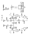
- FIG. 3 shows the no-loss S-probe when these typical circuit parameters are employed in the configuration.
- the S-probe is a 6-port circuit; hence, in the procedure for the circuit oscillation analysis and design, when n S-probes are used, there is conducted multi-port analysis for about 6n ports; and in the large-signal analysis, a two-tone harmonic balance analysis is required; hence the analysis becomes considerably complex.
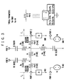
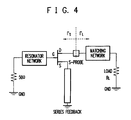
- FIG. 4 is a basic circuit layout diagram of an oscillator to be described here.
- An FET is used as an active element and a series feedback form in which a source terminal has a stub is employed in the circuit configuration.
- the S-probe is inserted in the gate terminal and the drain terminal of the oscillator to obtain the reflection coefficients toward the left and the right of the circuit therefrom.
- the reflection coefficient characteristic impedance
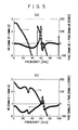
- FIG. 5( a ) and ( b ) illustrate a design (small signal) of the oscillation start based on the above oscillation condition in a specific oscillator circuit.
- FIG. 5( a ) shows a plotted result of the reflection coefficient at the gate terminal of the oscillator versus the frequency
- FIG. 5( b ) shows a plotted result of the reflection coefficient at the drain terminal.
- the S-probe causes no perturbation in the circuit (in particular, strictly no perturbation at small signal analysis); hence, for both of ( a ) and ( b ), the oscillation start condition is satisfied at one and the same frequency (about 62 GHz) according to the oscillation theory.
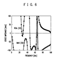
- FIG. 6 shows occurrence of negative resistance and a relation thereof to the oscillation start in the 60 GHz-OSC.
- Zd is a characteristic impedance obtained when viewing the active element side from the S-probe at the drain terminal.
- the real part of Zd in FIG. 6 indicates occurrence of negative resistance equal to or more than 50 ⁇ in a range from about 45 GHz to about 65 GHz.
- the imaginary part of Zd has a clear change point from “capacitive” to “inductive” near 62 GHz, and the change point is in the frequency band in which the negative resistance is taking place. That is, the change point indicates a frequency to cause oscillation; as for the small signal, it is also implied that this oscillator is capable of conducting stable oscillation.
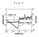
- FIG. 7 shows the reflection coefficient at the drain terminal at stationary oscillation of the 60 GHz-OSC in the above 2-tone harmonic balance method.
- the 60 GHz-OSC of this report oscillates at 59.88 GHz on the simulation and oscillation power is 13.2 dBm.
- a probing large signal of ⁇ 30 dBm is applied via the S-probe to the circuit to obtain the reflection coefficient for each frequency by sweeping the frequency. It is recognizable that the reflection coefficient characteristic and the phase characteristic of FIG. 7 satisfy expressions (B1) and (B2), which are to be satisfied by the oscillation stationary state at 60 GHz, according to the oscillation theory.
- the proposed no-loss S-probe on the circuit simulator can correctly obtain the reflection coefficients (impedances) at an arbitrary point of a circuit toward the left-hand section and the right-hand section of the circuit even in the large-signal state by using the negative resistance.
- the no-loss S-probe contributes to development of the oscillator design and to detection and suppression of parasitic oscillation of the amplifier.
- description has been first given of the principle of the no-loss P-probe method; additionally, for the exemplary embodiment 2, description has been given of an example in which the present invention is applied to the oscillator circuit design which is the basis of the oscillation analysis and design of the microwave circuit.
- Application to the amplifier will be described in conjunction with an exemplary embodiment 3 and a subsequent exemplary embodiment.
- a microwave amplifier is simply designed to have a gain in a band in which signals are to be amplified, the amplifier has an unnecessary gain outside the band in some cases.
- a millimeter-wave transistor since this transistor has a gain in a range up to a high frequency of the millimeter wave band, it naturally has a larger gain for less frequency; hence, the millimeter-wave transistor has an unnecessary gain outside the band. If such unnecessary gain outside the band satisfies the oscillation condition, a parasitic oscillation takes place.
- the amplifier parasitic oscillation is generally classified into even-mode oscillation and odd-mode oscillation (loop oscillation).
- the even mode oscillation is oscillation judged by a stability factor K.
- the odd-mode oscillation is oscillation which occurs when components connected in parallel to each other in a circuit are driven with mutually opposite phases and cannot be judged by the stability factors K or MU-value which is often used in general.
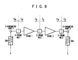
- FIG. 8 is a circuit diagram in which the no-perturbation S-probe is applied to the stability analysis for a multistage amplifier.
- the S-probe is inserted in a configuration in which the circuit component is sandwiched by the S-probe as shown in the diagram.
- the method of obtaining the reflection coefficient in a circuit cross section is based on the method described in detail in conjunction with the exemplary embodiment 1.
- the present method it is possible, without severing the particular loop of the circuit and without inserting a circulator therein, to calculate the reflection coefficient (characteristic impedance) in the small-signal state and the large-signal state by inserting the no-perturbation S-probe in the circuit, i.e., in a cross section of the circuit.
- the even-mode parasitic oscillation and odd-mode parasitic oscillation can be more correctly detected.
- stability of each stage of a multistage amplifier can be individually and quantitatively known according to expression (C1).
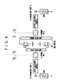
- FIG. 9 shows an equivalent circuit; this will be abbreviated as 60 GHz-AMP hereinbelow).
- FET field-effect transistor
- FIG. 9 shows an equivalent circuit; this will be abbreviated as 60 GHz-AMP hereinbelow.
- HJFET heterojunction FET
- the gate lead line a phase-restoring capacitor is formed for impedance matching.
- An equivalent circuit model of the FET employed for the calculation is constructed on the basis of measurement results of characteristics of an FET actually manufactured as a trial product through mass production processes for millimeter wave devices.
- an RC bias network is applied.
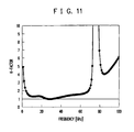
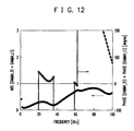
- FIG. 11 shows plotting of the stabilization factor K-value. The K-value shows, near 30 GHz, a low value about one, but the value is one or more for other frequencies; as far as it is seen from the drawing, the circuit stability seems to be almost secured.
- FIG. 12 shows a result of stability judgment based on expression (C1) or expressions (C4) and (C5).
- the S-probe is inserted in a location outside the loop circuit section of the FETs connected in parallel to each other and there exists no closed loop circuit section configured via the S-probe; hence, the detection of even-mode oscillation is carried out.
- the oscillation condition is not satisfied; hence, for the even-mode excitation, no danger of oscillation exists for the circuit, which is hence stable.
- a 60 GHz-AMP which is completely equal to FIGS. 8 and 9 excepting the balanced resistor, will be employed as an example.
- the S-probe is inserted in a closed loop section of the circuit in which odd-mode oscillation likely occurs as shown in an equivalent circuit of FIG. 13 .
- the small-signal characteristic and the stability factor K-value of this amplifier are completely equal to those shown respectively in FIGS. 10 and 11 regardless of presence or absence of the balanced resistor.
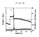
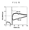
- FIG. 14 shows the stability factor according to expression (C1) or expressions (C4) and (C5) at the drain terminal by use of the S-probe when the balanced resistor is not applied. It can be seen that near 30 GHz, the conditions of the reflection coefficient and the phase almost satisfy the oscillation condition, and the 60 GHz-AMP is unstable near 30 GHz. To further check more precisely, the characteristic impedance Zd viewed from the drain terminal to the active element side is shown in FIG. 15 . According to FIG. 15 , it is recognized that the 60 GHz-AMP is not only unstable near 30 GHz, but also satisfies the oscillation condition, and has a danger to cause the odd-mode oscillation.
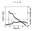
- FIG. 16 shows stability of the 60 GHz-AMP for the odd-mode oscillation when the balanced resistor 15 ⁇ is applied. As can be seen from FIG. 16 , it is known that as far as the small-signal level concerns, the odd-mode oscillation is suppressed by the balanced resistor.
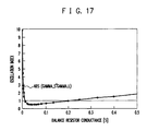
- the balanced resistor appropriately ranges from 15 ⁇ to 40 ⁇ , and 25 ⁇ is selected as an optimal value.
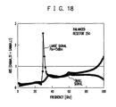
- FIG. 18 compares the reflection coefficient for each frequency in amplifier operation of the 60 GHz-AMP using a large-signal input with that in the small-signal operation.
- the calculation of the reflection coefficient for the large-signal input is a 2-tone harmonic balance analysis. It is assumed in the 2-tone analysis that the input large signal to the amplifier 60 GHz-AMP has a basic tone of 60 GHz and 15 dBm and the second-tone probe signal to be inputted to the S-probe by sweeping the frequency is ⁇ 30 dBm.
- the 60 GHz-AMP is stable for the odd-mode excitation in the small-signal operation by connecting the balanced resistor of 25 ⁇ as shown in FIG.
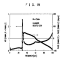
- the amplifier shows a stability factor K of one or more for all frequencies with the operation bias; although the operation is stable with a small signal, parasitic oscillation is shown when a large signal of a certain level is inputted in an ordinary operation. It can be hence considered that the parasitic oscillation of Table 1 is odd-mode oscillation (loop oscillation). It can be seen in this example that the method of this report is capable of also relatively quantitatively predicting and detecting parasitic oscillation.
- the parasitic oscillation of the amplifier in Table 1 experimentally and in the calculation, there regrettably exist both cases in which the parasitic oscillation is suppressed or not suppressed by the application of the balanced resistor.
- a highly accurate model as the large-signal model of the active element e.g., the EEHEMT model configured by use of ICCAP of Agilent.
- Stability of a circuit can be judged, according to the oscillation theory, by obtaining the reflection coefficients in the forward direction and the backward direction in an arbitrary cross section of the circuit.
- To obtain the reflection coefficients in the cross section of the circuit it is convenient to adopt the proposed no-loss S-probe which causes no loss even if it is inserted in the circuit and which is available in small-signal and large-signal operations.
- the circuit does not oscillate or the circuit oscillates, but does not conduct stable oscillation in many cases.
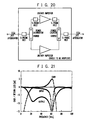
- FIG. 20 shows structure of a circuit for checking stability in the parallel-type amplifier.
- the signal attenuation quantity of the attenuator is set to zero.
- the oscillation condition is ordinarily satisfied in probe 2 (or 2 ′).
- the probe to calculate the reflection coefficient is ordinarily inserted in an output side of the active element (ordinarily, in the drain terminal for an FET).
- the probe to calculate the reflection coefficient is inserted in an input side of the active element (ordinarily, in the gate terminal for an FET)
- a method of power-coupling unitary amplifiers for which it has been confirmed that neither even-mode parasitic oscillation nor odd-mode parasitic oscillation occurs therein for power-coupling by use of a power distributing and coupling unit and a hybrid is regarded as an effective method to double the power from the amplifier while keeping the circuit stability secured.
- the power distributing and coupling unit and the hybrid have a function to distribute and to couple power in an operation band as well as a function to cut unnecessary signals outside the band; also, the Wilkinson power distributing and coupling unit or the like has also a function to isolate ports for signal coupling and distribution. It has been experimentally known that the feared loss in the power distributing and coupling can be simply reduced by devising the manufacturing of the power distributing and coupling unit such that the manufacturing is carried out according to designed values as strictly as possible; hence, it will not be a problem.
- every power distributing and coupling unit or hybrid can carry out some effect of the power coupling operation and the circuit stabilization. Accordingly, a method of selecting a circuit configuration by use of the method described above will be discussed hereinbelow in which difference in the stability of the parallel-structure amplifier, particularly, in the resistivity against the odd-mode excitation due to the kinds of the power distributing and coupling unit and the hybrid is compared to select a circuit configuration most favorable to the power coupling in accordance with each purpose.
- FET field-effect transistor
- HJFET heterojunction FET
- As the gate lead line a phase-restoring capacitor is formed for impedance matching.
- An RC bias network is applied to the bias circuit.
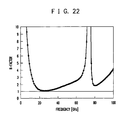
- FIG. 22 shows plotting of the stability factor K-value.
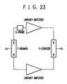
- an amplifier of FIG. 23 in which 60 GU-AMP are arranged in a parallel configuration by using a Y-branch (or a T-branch) including only simple wiring is considered.
- a Y-branch or a T-branch
- models constructed on the ADS are employed.
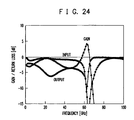
- FIG. 24 shows the small-signal characteristic of a Y-branch parallel amplifier. Since there exists input/output impedance mismatching due to the Y-branch, deterioration in the matching level is seen on the input side and a shift in the matching frequency is seen on the output side.
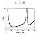
- FIG. 25 shows the stability factor K of the Y-branch parallel amplifier. Near 25 GHz, the K-value is about one, but the stability factor K indicates a value equal to or more than one for all frequencies ranging from DC to 100 GHz; it is hence known that this amplifier is stable for the even-mode excitation.
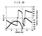
- FIG. 26 shows the stability for the odd-mode excitation of the Y-branch parallel amplifier based on expressions (D2) and (D3) by use of the S-probe inserted in the circuit as shown in FIG. 9 .
- the stability factor (D2) for the reflection coefficient is plotted; and along the right Y-axis, the phase condition (D3) is plotted.
- the oscillation start condition is satisfied at about 75 GHz in this amplifier and there exits danger of occurrence of odd-mode parasitic oscillation.
- the Y-branch has merits of the smallest circuit size and simple structure, but has not the isolation function between distributing (or coupling) ports; hence attention is to be given to that the odd-mode parasitic oscillation easily occurs in the Y-branch power distributing and coupling parallel amplifier as above.
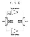
- FIG. 27 shows an amplifier shown in FIG. 27 in which 60 GU-AMP are arranged in a parallel configuration using the Wilkinson power distributing and coupling unit.
- 60 GHz-band Wilkinson power distributing and coupling unit and wiring sections models constructed on ADS are used.
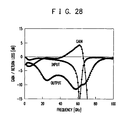
- FIG. 28 shows the small-signal characteristic of the Wilkinson-type parallel amplifier. A favorable matching characteristic is shown for both of the input and output sides.
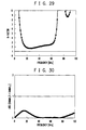
- FIG. 29 shows the stability factor K of the Wilkinson-type parallel amplifier. For all frequencies ranging from DC to 100 GHz, the stability factor K is more than one; it is hence recognizable that this amplifier is stable for the even-mode excitation.
- FIG. 30 shows the stability for the odd-mode excitation of the Wilkinson-type parallel amplifier based on expressions (D2) and (D3) by use of the S-probe inserted in the circuit as shown in FIG. 27 .
- the stability factor (D2) calculated from the reflection coefficient is sufficiently reduced to a value less than one in a wide band ranging from DC to 100 GHz; it can be hence recognized that this amplifier is fully stable for the odd-mode excitation.
- the isolation resistor has an isolation function not only for signals within the band, but also for signals with wider frequencies outside the band; hence, it can be considered that the amplifier constructed in the parallel structure by use of the Wilkinson power distribution and coupling unit has high stability in a wide band for the odd-mode excitation.
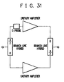
- FIG. 31 an amplifier shown in which 60 GU-AMP are disposed in a parallel configuration using a 90-degree hybrid is considered.
- a branch line coupler of 60 GHz-band operation is selected as the 90-degree hybrid.
- models constructed on ADS are used for the branch line coupler and wiring sections.
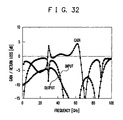
- FIG. 32 shows the small-signal characteristic of the 90-degree hybrid balance-type amplifier. Quite a favorable matching characteristic is shown in a sufficiently wide band for both of the input and output sides.
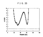
- FIG. 33 shows the stability factor K of the 90-degree hybrid balance-type amplifier.
- the stability factor K is more than one for all frequencies ranging from DC to 100 GHz, and it is hence recognized that this amplifier is stable for the even-mode excitation.
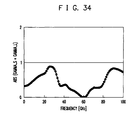
- FIG. 34 shows the stability for the odd-mode excitation of the 90-degree hybrid balance-type amplifier based on expressions (D2) and (D3) by use of the S-probe inserted in the circuit as shown in FIG. 31 .
- the stability factor (D2) calculated from the reflection coefficient is less than one in a wide band ranging from DC to 100 GHz; it is hence recognizable that this amplifier is fully stable for the odd-mode excitation.
- the stability factor (D2) according to the reflection coefficient is in the vicinity of one, and an unnecessary gain is attained also in FIG. 32 ; hence, it cannot be asserted that sufficient stability is secured in the large-signal input operation.
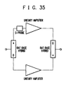
- FIG. 35 a push-pull amplifier shown in FIG. 35 in which 60 GU-AMP are disposed in a parallel configuration by use of a 180-degree hybrid is considered.
- the push-pull amplifier generally has a merit in which higher harmonics of even-numbered degrees cancel out in the output wave.
- a rat-race hybrid of 60 GHz-band operation is selected as the 180-degree hybrid.
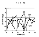
- FIG. 36 shows the small-signal characteristic of the 180-degree hybrid push-pull amplifier. A favorable matching characteristic is shown for both of the input and output sides.
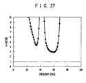
- FIG. 37 shows the stability factor K of the 180-degree hybrid push-pull amplifier.
- the stability factor K is more than one for all frequencies ranging from DC to 100 GHz, and it can be hence recognized that this amplifier is stable for the even-mode excitation.
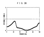
- FIG. 38 shows the stability for the odd-mode excitation of the 180-degree hybrid push-pull amplifier based on expressions (D2) and (D3) by use of the S-probe inserted in the circuit as shown in FIG. 34 .
- the stability factor (D2) calculated from the reflection coefficient is less than one in a wide band ranging from DC to 100 GHz; it is hence recognizable that this amplifier is stable for the odd-mode excitation.
- the stability factor according to the reflection coefficient is in the vicinity of one for frequencies near 25 GHz; hence, it cannot be simply asserted that this amplifier, like the 90-degree hybrid balance-type amplifier, is fully stable in the large-signal operation.
- rat-race hybrid 38 is obtained by using a rat-race hybrid in which a certain degree of isolation is provided between the distribution (or coupling) ports is employed as the 180-degree hybrid.
- a rat-race hybrid in which a certain degree of isolation is provided between the distribution (or coupling) ports is employed as the 180-degree hybrid.
- the isolation between the distribution (or coupling) ports is insufficient, i.e., about 5 dB; hence, the stability in the large-signal operation is less secured when compared with the case in which the rat-race hybrid is adopted.
- the unitary amplifiers are mutually excited with the reverse phases in the regular operation mode. Therefore, it can also be considered that the push-pull amplifier is easily odd-mode excited.
- the method intentionally adopting the push-pull-type parallel amplifier in which odd-mode excitation easily occurs is also effective.
- the circuits or methods of the present invention are capable of correctly obtaining the reflection coefficient (characteristic impedance) in the large-signal state of a circuit; hence, the circuits or methods make the design of the oscillator more precise as well as give us important knowledge regarding the stability of a multistage amplifier, loop oscillation in an amplifier, the stability of a balance-type amplifier, and the like. Therefore, the circuits or methods of the present invention advantageously contribute to the designs and evaluations of an amplifier, an oscillator, and the like which operates in a microwave or millimeter-wave band.
- FIG. 1 is a diagram showing a circuit configuration of a relevant S-probe.
- FIG. 2 is a diagram showing a general circuit configuration of a proposed no-loss S-probe.
- FIG. 3 is a diagram showing a typical circuit configuration of a proposed no-loss S-probe.
- FIG. 4 is a diagram showing a basic circuit configuration of an oscillator.
- FIG. 5 is a diagram showing designs of oscillation start of an oscillator; ( a ) viewed at the gate terminal and ( b ) viewed at the drain terminal.
- FIG. 6 is a diagram showing the analysis and the design of the negative resistor.
- FIG. 7 is a diagram showing the characteristic at stationary oscillation by the large-signal analysis.
- FIG. 8 is a diagram showing the amplifier stability analysis by an S-probe.
- FIG. 9 is a diagram showing detection (equivalent circuit) of even-mode oscillation in an S-probe method.
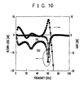
- FIG. 10 is a diagram showing the small-signal characteristic of a 60 GHz amplifier.
- FIG. 11 is a diagram showing the stability factor K of the 60 GHz amplifier.
- FIG. 12 is a diagram showing the stability of the 60 GHz amplifier in the even mode.
- FIG. 13 is a diagram showing detection (equivalent circuit) of odd-mode oscillation by an S-probe method.
- FIG. 14 is a diagram showing the stability (“without” balanced resistor) for odd-mode excitation of the 60 GHz amplifier.
- FIG. 15 is a diagram showing odd-mode excitation (without balanced resistor) of the 60 GHz amplifier.
- FIG. 16 is a diagram showing the stability (“with” balanced resistor) for odd-mode excitation of the 60 GHz amplifier.
- FIG. 17 is a diagram showing an optimal design of the balanced resistor value.
- FIG. 18 is a diagram showing comparison between the small-signal input and the large-signal operation input.
- FIG. 19 is a diagram showing the stability when a large signal is inputted.
- FIG. 20 is a diagram showing a stability checking circuit configuration in a parallel-type amplifier.
- FIG. 21 is a diagram showing the small-signal characteristic of a unitary amplifier.
- FIG. 22 is a diagram showing the stability factor K of the unitary amplifier.
- FIG. 23 is a diagram showing a parallel amplifier employing a Y-branch.
- FIG. 24 is a diagram showing the small-signal characteristic of the Y-branch parallel amplifier.
- FIG. 25 is a diagram showing the stability factor K of the Y-branch parallel amplifier.
- FIG. 26 is a diagram showing the odd-mode stability of the Y-branch parallel amplifier.
- FIG. 27 is a diagram showing a parallel amplifier using a Wilkinson power distributing and coupling unit.
- FIG. 28 is a diagram showing the small-signal characteristic of the Wilkinson-type parallel amplifier.
- FIG. 29 is a diagram showing the stability factor K of the Wilkinson-type parallel amplifier.
- FIG. 30 is a diagram showing the odd-mode stability of the Wilkinson-type parallel amplifier.
- FIG. 31 is a diagram showing a balance-type amplifier using a 90-degree hybrid.
- FIG. 32 is a diagram showing the small-signal characteristic of the balance-type amplifier using a 90-degree hybrid.
- FIG. 33 is a diagram showing the stability factor K of the balance-type amplifier using a 90-degree hybrid.
- FIG. 34 is a diagram showing the odd-mode stability of the balance-type amplifier using a 90-degree hybrid.
- FIG. 35 is a diagram showing a push-pull amplifier using a 180-degree hybrid.
- FIG. 36 is a diagram showing the small-signal characteristic of the push-pull amplifier using a 180-degree hybrid.
- FIG. 37 is a diagram showing the stability factor K of the push-pull amplifier using a 180-degree hybrid.
- FIG. 38 is a diagram showing the odd-mode stability of the push-pull amplifier using a 180-degree hybrid.
Landscapes
- Engineering & Computer Science (AREA)
- Computer Hardware Design (AREA)
- Physics & Mathematics (AREA)
- Theoretical Computer Science (AREA)
- Evolutionary Computation (AREA)
- Geometry (AREA)
- General Engineering & Computer Science (AREA)
- General Physics & Mathematics (AREA)
- Microelectronics & Electronic Packaging (AREA)
- Tests Of Electronic Circuits (AREA)
- Measurement Of Resistance Or Impedance (AREA)
Abstract
Description
Va=Vb+I 2 ·Rx=Vb(Z 2 +Rx)/Z 2
Vb=I 2 ·Z 2.
V 3 =−M 3 ·Vr=−M 3(Va−Vb)=−VaM 3 Rx/(Z 2 +Rx)
V 4 =−M 4 ·Vb.
S 36 =V 3 /V 6 =−VaM 3 Rx/[V 6(Z 2 +Rx)]
S 46 =V 4 /V 6 =−M 4 Z 2 Va/[V 6(Z 2 +Rx)].
Va=I 1 Z 1
Vb=Va+I 1 Rx=Va(Z 1 +Rx)/Z 1.
V 3 =−M 3 Vr=−M 3(Vb−Va)=VaM 3 Rx/(Z 1 +Rx)
V 4 =−M 4 Vb.
S 35 =V 3 /V 5 =−VbM 3 Rx/[V 5(Z 1 +Rx)]
S 45 =V 4 /V 5 =M 4 Vb/V 5.
In consequence,
S 46 /S 36 =M 4 Z 2 /M 3 Rx
S 45 /S 35 =−M 4(Z 1 +Rx)/(M 3 Rx).
In the expression,
M 4/(M 3 Rx)=1
0<R<<1.
Rs=10 MΩ
Rv=10 MΩ
Rx=100μΩ
M 3=1000
M 4=1,
there are obtained
Z 1 =−S 45 /S 35
Z 2 =S 46 /S 36.
ΓS=(Z 1 −Z 0)/(Z 1 +Z 0)
ΓL=(Z 2 −Z 0)/(Z 2 +Z 0).
Here, Z0 is system impedance and inner resistance of the S parameter probe and is ordinarily 50 Ω.
Rs=10 MΩ
Rx=1 Ω
M=1
α=½.
Z 1 =−S[4,5]S[3,5]−Rx/2
Z 2 =S[4,6]/S[3,6]+Rx/2.
Therefore, viewing the circuit side, the forward and backward reflection coefficients ΓS, ΓL are respectively attained as
ΓS=(Z 1 −Z 0)/(Z 1 +Z 0)
ΓL=(Z 2 −Z 0)/(Z 2 +Z 0).
Here, Z0 is system impedance and internal resistance of the S parameter probe which is ordinarily 50 Ω.
S[3,6]=V 3 /V 6 =V A MRx/{V 6(Z 2 +αRx)}
S[4,6]=V 4 /V 6 =[Z 2+(α−1)Rx]V A /[VV 6(Z 2 +αRx)].
S[3,6]=V 3 /V 5 =−V B MRx/[V 5 {Z 1+(1−α)Rx}]
S[4,5]=V 4 /V 5 =V B /V 5.
As a result,
S[4/6]/S[3,6]=[Z 2+(α−1)Rx]/(MRx)
S[4/5]/S[3,5]=−[Z 1+(1−α)Rx]/(MRx).
Z 1 =−S[4,5]/S[3,5]−(1−α)Rx
Z 2 =S[4,6]/S[3,6]+(1−α)Rx.
ΓS=(Z 1 −Z 0)/(Z 1 +Z 0)
ΓL=(Z 2 −Z 0)/(Z 2 +Z 0).
Here, Z0 is system impedance and inner resistance of the S parameter probe and is ordinarily 50 Ω.
Z 1 =−V45/V 35−(1−α)Rx
Z 2 =V46/V36+(1−α)Rx.
Rs=10 MΩ
Rx=1 Ω
M=1
α=½.
Y[1,1]=−1/αRx, Y[1,2]=1/αRx
Y[2,1]=1/αRx, Y[2,2]=−1/αRx;
to obtain, for example, the negative resistance −Rx/2, it is only necessary to set
Y[1,2]=−2/Rx, Y[1,2]=2/Rx
Y[2,1]=2/Rx, Y[2,2]=−2/Rx
as shown on the right side of
abs(ΓS1ΓL1)>1 and
phase(ΓS1)+phase(ΓL1)=0.
This is equivalent to the oscillation start condition when the characteristic impedances obtained by viewing the active element side and the load element side are set as Zout and ZL, namely,
Re{Z out(ω)}<0 and |Re{Z out(ω)}|>Re{Z L(ω)}
Im{Z out(ω)}+Im{Z L(ω)}=0,
but it is more simply expressed.
abs(ΓS1ΓL1)=1 (B1)
phase(ΓS1)+phase(ΓL1)=0 (B2).
Re{Z out(ω0)}<0 and |Re{Z out(ω0)}|=Re{Z L(ω0)}
Im{Z out(ω0)}+Im{Z L(ω0)}=0,
but it is more simply expressed.
abs{ΓS(i-1)*ΓL(i-1)}<1 and abs(ΓSi*ΓLi)<1 (C1)
is required. (Since the active element is actually not unilateral, only either one the former and latter expressions may also be ordinarily used for the two expressions). The condition required to make the overall circuit of an n-stage amplifier stable is, since each stage is required to be stable in general,
and abs(ΓS0*ΓL0)<1
and abs(ΓS1*ΓL1)<1
. . .
and abs(ΓSn*ΓLn)<1 (C2)
These form a condition more severe than that of the expression of the type of
Real(ΓSi*ΓLi)<1 (C3)
of the original paper [1] of Wang et al; however, since there takes place an inconsistency wherein even if expression (C3) is satisfied, there exists a case in which an oscillation condition is satisfied according to the oscillation theory; this report hence adopts, as the stability judging formula, expression (C1) or (C2) which is faithful to the oscillation theory.
abs(ΓS1*ΓL1)>1 (C4)
phase(ΓS1)+phase(ΓLi)=0 (C5)
are satisfied.
| TABLE 1 | |||
| Experimental values | Calculated values | ||
| V-band amplifier | 32.178 | GHz | 30.0 | GHz | ||
| C-band amplifier | 1.514 | 1.4 | ||||
| 3.104 | 3.2 | |||||
| 7.041 | 6.9 | |||||
abs(ΓS*ΓL)<1 (D1)
holds at any virtual cross-sectional point of the circuit. Additionally, to make the circuit be about to oscillate, it is required that
abs(ΓS*ΓL)>1 (D2) and
phase(ΓS)+phase(ΓL)=0 (D3)
hold at a virtual cross-sectional point in the small-signal state. In the stationary oscillation state in which the circuit oscillates continuously,
abs(ΓS*ΓL)=1 (D4) and
phase(ΓS)+phase(ΓL)=0 (D5)
hold at any virtual cross-sectional point in the large-signal state. If the stability condition of expression (D1) is not satisfied as well as the stability conditions of expressions (D2) and (D3) are not satisfied at a virtual cross-sectional point in the circuit, the circuit does not oscillate or the circuit oscillates, but does not conduct stable oscillation in many cases.
Claims (10)
Applications Claiming Priority (3)
| Application Number | Priority Date | Filing Date | Title |
|---|---|---|---|
| JP2006-314700 | 2006-11-21 | ||
| JP2006314700 | 2006-11-21 | ||
| PCT/JP2007/069394 WO2008062607A1 (en) | 2006-11-21 | 2007-10-03 | Rf circuit, circuit evaluating method, algorithm and recording medium |
Publications (2)
| Publication Number | Publication Date |
|---|---|
| US20100064265A1 US20100064265A1 (en) | 2010-03-11 |
| US8245179B2 true US8245179B2 (en) | 2012-08-14 |
Family
ID=39429548
Family Applications (2)
| Application Number | Title | Priority Date | Filing Date |
|---|---|---|---|
| US12/312,551 Expired - Fee Related US8245179B2 (en) | 2006-11-21 | 2007-10-03 | RF circuit, circuit evaluation method, algorithm and recording medium |
| US13/539,637 Expired - Fee Related US8458644B2 (en) | 2006-11-21 | 2012-07-02 | RF circuit, circuit evaluation method, algorithm and recording medium |
Family Applications After (1)
| Application Number | Title | Priority Date | Filing Date |
|---|---|---|---|
| US13/539,637 Expired - Fee Related US8458644B2 (en) | 2006-11-21 | 2012-07-02 | RF circuit, circuit evaluation method, algorithm and recording medium |
Country Status (3)
| Country | Link |
|---|---|
| US (2) | US8245179B2 (en) |
| JP (1) | JP4985654B2 (en) |
| WO (1) | WO2008062607A1 (en) |
Cited By (5)
| Publication number | Priority date | Publication date | Assignee | Title |
|---|---|---|---|---|
| US20100231236A1 (en) * | 2009-03-12 | 2010-09-16 | Sige Semiconductor Inc. | Integrated VSWR Detector for Monolithic Microwave Integrated Circuits |
| US8935133B1 (en) * | 2012-03-26 | 2015-01-13 | The Mathworks, Inc. | Measurement points in modeling and simulation |
| US8970297B2 (en) | 2012-03-19 | 2015-03-03 | Qualcomm Incorporated | Reconfigurable input power distribution doherty amplifier with improved efficiency |
| US9031518B2 (en) | 2012-12-17 | 2015-05-12 | Qualcomm Incorporated | Concurrent hybrid matching network |
| US9306502B2 (en) | 2011-05-09 | 2016-04-05 | Qualcomm Incorporated | System providing switchable impedance transformer matching for power amplifiers |
Families Citing this family (6)
| Publication number | Priority date | Publication date | Assignee | Title |
|---|---|---|---|---|
| JP5306896B2 (en) * | 2009-05-14 | 2013-10-02 | 三菱電機株式会社 | Oscillation analyzer and program thereof |
| KR20130076597A (en) * | 2011-12-28 | 2013-07-08 | 삼성전기주식회사 | Differential mode amplifier driving circuit |
| EP3373017B1 (en) * | 2017-03-07 | 2024-05-29 | Nxp B.V. | A testing system for millimetre wave packaged integrated circuits |
| US10496587B1 (en) * | 2018-06-27 | 2019-12-03 | Integrated Device Technology, Inc. | Wide programmable gain receiver data path for single-ended memory interface application |
| US11397204B2 (en) * | 2019-11-26 | 2022-07-26 | Achronix Semiconductor Corporation | Noise-independent loss characterization of networks |
| KR102766085B1 (en) * | 2020-07-16 | 2025-02-12 | 삼성전자 주식회사 | Method and apparatus for detecting circuit defects |
Citations (6)
| Publication number | Priority date | Publication date | Assignee | Title |
|---|---|---|---|---|
| JPH08274584A (en) | 1995-02-01 | 1996-10-18 | Nippon Telegr & Teleph Corp <Ntt> | Active inductor |
| US5654679A (en) * | 1996-06-13 | 1997-08-05 | Rf Power Products, Inc. | Apparatus for matching a variable load impedance with an RF power generator impedance |
| US5726613A (en) | 1995-02-01 | 1998-03-10 | Nippon Telegraph And Telephone Corporation | Active inductor |
| JP2000114507A (en) | 1998-10-02 | 2000-04-21 | Sony Corp | Method for simulating semiconductor element |
| JP2001177580A (en) | 1999-12-20 | 2001-06-29 | Sony Corp | Impedance adapting system |
| JP2002169851A (en) | 2000-12-04 | 2002-06-14 | Agilent Technologies Japan Ltd | Method and instrument for measuring electric circuit, method and device for designing electric circuit, recording medium with this measuring method recorded, and recording medium with this design method recorded |
Family Cites Families (2)
| Publication number | Priority date | Publication date | Assignee | Title |
|---|---|---|---|---|
| JPS5543848Y2 (en) * | 1976-05-15 | 1980-10-15 | ||
| US6369603B1 (en) * | 1997-09-02 | 2002-04-09 | Midwest Research Institute | Radio frequency coupling apparatus and method for measuring minority carrier lifetimes in semiconductor materials |
-
2007
- 2007-10-03 US US12/312,551 patent/US8245179B2/en not_active Expired - Fee Related
- 2007-10-03 WO PCT/JP2007/069394 patent/WO2008062607A1/en active Application Filing
- 2007-10-03 JP JP2008545331A patent/JP4985654B2/en not_active Expired - Fee Related
-
2012
- 2012-07-02 US US13/539,637 patent/US8458644B2/en not_active Expired - Fee Related
Patent Citations (7)
| Publication number | Priority date | Publication date | Assignee | Title |
|---|---|---|---|---|
| JPH08274584A (en) | 1995-02-01 | 1996-10-18 | Nippon Telegr & Teleph Corp <Ntt> | Active inductor |
| US5726613A (en) | 1995-02-01 | 1998-03-10 | Nippon Telegraph And Telephone Corporation | Active inductor |
| US5654679A (en) * | 1996-06-13 | 1997-08-05 | Rf Power Products, Inc. | Apparatus for matching a variable load impedance with an RF power generator impedance |
| JP2000114507A (en) | 1998-10-02 | 2000-04-21 | Sony Corp | Method for simulating semiconductor element |
| JP2001177580A (en) | 1999-12-20 | 2001-06-29 | Sony Corp | Impedance adapting system |
| JP2002169851A (en) | 2000-12-04 | 2002-06-14 | Agilent Technologies Japan Ltd | Method and instrument for measuring electric circuit, method and device for designing electric circuit, recording medium with this measuring method recorded, and recording medium with this design method recorded |
| US6571372B2 (en) | 2000-12-04 | 2003-05-27 | Agilent Technologies, Inc. | Method and apparatus for measuring and designing electric circuit based on two-port network thereof, and computer-readable recording medium for recording the same |
Non-Patent Citations (3)
| Title |
|---|
| K. Wang et al., "The S-Probe a New, Cost-Effective, 4-Gamma Method for Evaluating Multi-Stage Amplifier Stability", 1992 MTT-S Digest, pp. 829-832. |
| Notification of Reasons for Rejection dated Jan. 24, 2012 (with a partial English translation). |
| Wang, K. et al. The S-probe-a new, cost-effective, 4-gamma method for evaluating multi-stage amplifier stability, Microwave Symposium Digest, 1992, IEEE MTT-S International, United States, IEEE, Jun. 1, 1992, vol. 2, pp. 829-832. ISSN: 0149-645X. |
Cited By (6)
| Publication number | Priority date | Publication date | Assignee | Title |
|---|---|---|---|---|
| US20100231236A1 (en) * | 2009-03-12 | 2010-09-16 | Sige Semiconductor Inc. | Integrated VSWR Detector for Monolithic Microwave Integrated Circuits |
| US8723531B2 (en) * | 2009-03-12 | 2014-05-13 | Sige Semiconductor, Inc. | Integrated VSWR detector for monolithic microwave integrated circuits |
| US9306502B2 (en) | 2011-05-09 | 2016-04-05 | Qualcomm Incorporated | System providing switchable impedance transformer matching for power amplifiers |
| US8970297B2 (en) | 2012-03-19 | 2015-03-03 | Qualcomm Incorporated | Reconfigurable input power distribution doherty amplifier with improved efficiency |
| US8935133B1 (en) * | 2012-03-26 | 2015-01-13 | The Mathworks, Inc. | Measurement points in modeling and simulation |
| US9031518B2 (en) | 2012-12-17 | 2015-05-12 | Qualcomm Incorporated | Concurrent hybrid matching network |
Also Published As
| Publication number | Publication date |
|---|---|
| US20100064265A1 (en) | 2010-03-11 |
| WO2008062607A1 (en) | 2008-05-29 |
| US20120278785A1 (en) | 2012-11-01 |
| US8458644B2 (en) | 2013-06-04 |
| JPWO2008062607A1 (en) | 2010-03-04 |
| JP4985654B2 (en) | 2012-07-25 |
Similar Documents
| Publication | Publication Date | Title |
|---|---|---|
| US8245179B2 (en) | RF circuit, circuit evaluation method, algorithm and recording medium | |
| US8952752B1 (en) | Smart power combiner | |
| US20040174172A1 (en) | Method of correcting measurement error and electronic component characteristic measurement apparatus | |
| Donahue et al. | Power amplifier with load impedance sensing incorporated into the output matching network | |
| Marzall et al. | Active MMIC circulator performance in a phased-array-like environment | |
| Deferm et al. | Differential and common mode stability analysis of differential mm-wave CMOS amplifiers with capacitive neutralization | |
| John et al. | Investigation of compact power amplifier cells at THz frequencies using InGaAs mHEMT technology | |
| JP2009522572A (en) | Method and apparatus for determining non-linear behavior | |
| Collantes et al. | Monte-Carlo stability analysis of microwave amplifiers | |
| Hanson et al. | An improved de-embedding technique for the measurement of the complex constitutive parameters of materials using a stripline field applicator | |
| Ayllon et al. | Sensitivity enhancement in pole-zero identification based stability analysis of microwave circuits | |
| Griffith et al. | A 227.5 GHz InP HBT SSPA MMIC with 101mW Pout at 14.0 dB compressed gain and 4.04% PAE | |
| Joudeh et al. | A linear simulation technique for a power traveling-wave amplifier | |
| Epp et al. | A generalized scattering matrix approach for analysis of quasi-optical grids and de-embedding of device parameters | |
| Wang et al. | Improved measurement techniques for high-power transistor modeling | |
| Squartecchia et al. | 75 GHz InP DHBT power amplifier based on two-stacked transistors | |
| Iqbal et al. | Analytical expression for the equivalent input noise current spectral density of HBT distributed amplifier based optical receivers | |
| Li et al. | A Gallium Nitride (GaN) Doherty power amplifier chip design based on series RC stability network | |
| Issaoun et al. | Simple Small-Signal HEMT Model Suitable for GaN Stability Analysis and Technologies Benchmarking | |
| Korotaev et al. | Research of directional microwave couplers under conditions of extreme changes in load parameters caused by active element failures and circuit breaks | |
| Huang et al. | A six-port coupler with high directivity for VSWR measurement | |
| Call et al. | Large-signal scattering parameter measurements for RF power transistors | |
| Simbélie et al. | Nonlinear electrical modeling of MASMOS structures with a conventional 3-port topoloy approach | |
| Greda et al. | Efficient analysis of waveguide-to-microstrip and waveguide-to-coplanar line transitions | |
| CN118657101A (en) | A fast extraction method of behavioral model parameters based on real-time evaluation technology |
Legal Events
| Date | Code | Title | Description |
|---|---|---|---|
| AS | Assignment |
Owner name: NEC CORPORATION,JAPAN Free format text: ASSIGNMENT OF ASSIGNORS INTEREST;ASSIGNOR:INOUE, TAKASHI;REEL/FRAME:022713/0370 Effective date: 20090508 Owner name: NEC CORPORATION, JAPAN Free format text: ASSIGNMENT OF ASSIGNORS INTEREST;ASSIGNOR:INOUE, TAKASHI;REEL/FRAME:022713/0370 Effective date: 20090508 |
|
| REMI | Maintenance fee reminder mailed | ||
| LAPS | Lapse for failure to pay maintenance fees | ||
| STCH | Information on status: patent discontinuation |
Free format text: PATENT EXPIRED DUE TO NONPAYMENT OF MAINTENANCE FEES UNDER 37 CFR 1.362 |
|
| FP | Expired due to failure to pay maintenance fee |
Effective date: 20160814 |