EP2803988B1 - Nanostrukturierte Mikroelektroden und Bioerfassungsvorrichtungen damit - Google Patents
Nanostrukturierte Mikroelektroden und Bioerfassungsvorrichtungen damit Download PDFInfo
- Publication number
- EP2803988B1 EP2803988B1 EP14176968.7A EP14176968A EP2803988B1 EP 2803988 B1 EP2803988 B1 EP 2803988B1 EP 14176968 A EP14176968 A EP 14176968A EP 2803988 B1 EP2803988 B1 EP 2803988B1
- Authority
- EP
- European Patent Office
- Prior art keywords
- microelectrode
- nanostructured
- lead
- nme
- biosensing
- Prior art date
- Legal status (The legal status is an assumption and is not a legal conclusion. Google has not performed a legal analysis and makes no representation as to the accuracy of the status listed.)
- Not-in-force
Links
Images


Classifications
-
- G—PHYSICS
- G01—MEASURING; TESTING
- G01N—INVESTIGATING OR ANALYSING MATERIALS BY DETERMINING THEIR CHEMICAL OR PHYSICAL PROPERTIES
- G01N27/00—Investigating or analysing materials by the use of electric, electrochemical, or magnetic means
- G01N27/26—Investigating or analysing materials by the use of electric, electrochemical, or magnetic means by investigating electrochemical variables; by using electrolysis or electrophoresis
- G01N27/28—Electrolytic cell components
- G01N27/30—Electrodes, e.g. test electrodes; Half-cells
- G01N27/327—Biochemical electrodes, e.g. electrical or mechanical details for in vitro measurements
- G01N27/3271—Amperometric enzyme electrodes for analytes in body fluids, e.g. glucose in blood
- G01N27/3272—Test elements therefor, i.e. disposable laminated substrates with electrodes, reagent and channels
-
- G—PHYSICS
- G01—MEASURING; TESTING
- G01N—INVESTIGATING OR ANALYSING MATERIALS BY DETERMINING THEIR CHEMICAL OR PHYSICAL PROPERTIES
- G01N27/00—Investigating or analysing materials by the use of electric, electrochemical, or magnetic means
- G01N27/26—Investigating or analysing materials by the use of electric, electrochemical, or magnetic means by investigating electrochemical variables; by using electrolysis or electrophoresis
- G01N27/28—Electrolytic cell components
- G01N27/30—Electrodes, e.g. test electrodes; Half-cells
- G01N27/327—Biochemical electrodes, e.g. electrical or mechanical details for in vitro measurements
- G01N27/3275—Sensing specific biomolecules, e.g. nucleic acid strands, based on an electrode surface reaction
- G01N27/3278—Sensing specific biomolecules, e.g. nucleic acid strands, based on an electrode surface reaction involving nanosized elements, e.g. nanogaps or nanoparticles
-
- G—PHYSICS
- G01—MEASURING; TESTING
- G01N—INVESTIGATING OR ANALYSING MATERIALS BY DETERMINING THEIR CHEMICAL OR PHYSICAL PROPERTIES
- G01N27/00—Investigating or analysing materials by the use of electric, electrochemical, or magnetic means
- G01N27/26—Investigating or analysing materials by the use of electric, electrochemical, or magnetic means by investigating electrochemical variables; by using electrolysis or electrophoresis
- G01N27/28—Electrolytic cell components
- G01N27/30—Electrodes, e.g. test electrodes; Half-cells
- G01N27/327—Biochemical electrodes, e.g. electrical or mechanical details for in vitro measurements
- G01N27/3275—Sensing specific biomolecules, e.g. nucleic acid strands, based on an electrode surface reaction
-
- G—PHYSICS
- G01—MEASURING; TESTING
- G01N—INVESTIGATING OR ANALYSING MATERIALS BY DETERMINING THEIR CHEMICAL OR PHYSICAL PROPERTIES
- G01N33/00—Investigating or analysing materials by specific methods not covered by groups G01N1/00 - G01N31/00
- G01N33/48—Biological material, e.g. blood, urine; Haemocytometers
- G01N33/50—Chemical analysis of biological material, e.g. blood, urine; Testing involving biospecific ligand binding methods; Immunological testing
- G01N33/53—Immunoassay; Biospecific binding assay; Materials therefor
- G01N33/543—Immunoassay; Biospecific binding assay; Materials therefor with an insoluble carrier for immobilising immunochemicals
- G01N33/54366—Apparatus specially adapted for solid-phase testing
- G01N33/54373—Apparatus specially adapted for solid-phase testing involving physiochemical end-point determination, e.g. wave-guides, FETS, gratings
- G01N33/5438—Electrodes
-
- Y—GENERAL TAGGING OF NEW TECHNOLOGICAL DEVELOPMENTS; GENERAL TAGGING OF CROSS-SECTIONAL TECHNOLOGIES SPANNING OVER SEVERAL SECTIONS OF THE IPC; TECHNICAL SUBJECTS COVERED BY FORMER USPC CROSS-REFERENCE ART COLLECTIONS [XRACs] AND DIGESTS
- Y10—TECHNICAL SUBJECTS COVERED BY FORMER USPC
- Y10S—TECHNICAL SUBJECTS COVERED BY FORMER USPC CROSS-REFERENCE ART COLLECTIONS [XRACs] AND DIGESTS
- Y10S977/00—Nanotechnology
- Y10S977/70—Nanostructure
- Y10S977/754—Dendrimer, i.e. serially branching or "tree-like" structure
-
- Y—GENERAL TAGGING OF NEW TECHNOLOGICAL DEVELOPMENTS; GENERAL TAGGING OF CROSS-SECTIONAL TECHNOLOGIES SPANNING OVER SEVERAL SECTIONS OF THE IPC; TECHNICAL SUBJECTS COVERED BY FORMER USPC CROSS-REFERENCE ART COLLECTIONS [XRACs] AND DIGESTS
- Y10—TECHNICAL SUBJECTS COVERED BY FORMER USPC
- Y10S—TECHNICAL SUBJECTS COVERED BY FORMER USPC CROSS-REFERENCE ART COLLECTIONS [XRACs] AND DIGESTS
- Y10S977/00—Nanotechnology
- Y10S977/902—Specified use of nanostructure
- Y10S977/904—Specified use of nanostructure for medical, immunological, body treatment, or diagnosis
- Y10S977/925—Bioelectrical
Definitions
- Genomic analysis is revolutionizing early disease diagnosis and dramatically enhancing patient care ( McGuire et al. Science 317:1687 , Srinivas et al., Lancet Oncol. 2:698 ).
- Microarrays Drmanac et al., Science 260:1649 , Hacia et al., Nat. Genet. 14:441
- PCR polymerase chain reaction
- Saiki et al., Science 230:1350 have, as tools, helped to spearhead this revolution, enabling the discovery and the initial development of assays for patient testing ( Morris et al., Curr. Opin. Oncol. 19:547 ).
- Biomarker analysis based on electronic readout has long been cited as a promising approach that would enable a new family of chip-based devices with appropriate cost and sensitivity for medical testing ( Drummond et al., Nat. Biotechnol. 21:1192 , Katz et al., Electroanalysis 15: 913 ).
- the sensitivity of electronic readout is in principle sufficient to allow direct detection of small numbers of analyte molecules with simple instrumentation.
- Clack et al., Nat. Biotechnol. 26:825 Geiss et al., Nat. Biotechnol. 26:317 , Hahm et al., Nano Lett.
- nanowire electrodes for ultrasensitive nucleic acids and protein detection has been investigated ( Gasparac et al. J Am Chem Soc 126:12270 ).
- the use of this electrode platform enables the electrochemical detection of picomolar levels of analytes, a level of sensitivity that is not possible using macroscale materials.
- nanowires are able to detect attomolar levels of analytes, this actually corresponds to picomolar levels when dealing with the volumes typically used for analysis.
- nanoparticle-modified electrodes may exhibit several advantages over conventional macroelectrodes such as enhancement of mass transport, catalysis, high effective surface area and control over electrode microenvironment ( Katz et al. Electroanalysis 2004, 16, 19-44 , Welch et al. Anal. Bioanal. Chem. 2006, 384, 601-619 ). Manufacturing arrays of nanowire electrodes, however, is non-trivial.
- a biosensing device comprises a substrate, at least one electrically conductive lead on the substrate, an insulating layer covering the lead, insulating layer having an aperture defining a space in which a portion of the lead is exposed, and a nanostructured microelectrode deposited within the aperture, wherein the microelectrode is adapted by means of an electrocatalytic reporter system to generate a charge in response to a biomolecular stimulus, wherein the nanostructured microelectrode is capable of presenting a biomolecular probe at the surface thereof, and the nanostructured microelectrode is in electrical contact with the exposed portion of the lead.
- Nanostructured microelectrodes are electrodes which are nanotextured and thus have an increased surface area.
- Preferred NMEs are comprised of a noble metal, (e.g. gold, platinum, palladium, silver, osmium, indium, rhodium, ruthenium); alloys of noble metals (e.g. gold-palladium, silver- platinum, etc.); conducting polymers (e.g. polypyrole (PPY)); non-noble metals (e.g. copper, nickel, aluminum, tin, titanium, indium, tungsten, platinum); metal oxides (e.g.
- a noble metal e.g. gold, platinum, palladium, silver, osmium, indium, rhodium, ruthenium
- alloys of noble metals e.g. gold-palladium, silver- platinum, etc.
- conducting polymers e.g. polypyrole (PPY)
- non-noble metals e.g.
- NMEs of the above-described materials are highly conductive and form strong bonds with probes (e.g. nucleic acids and peptides).
- NMEs have a height in the range of about 0.5 to about 100 microns (pm), for example in the range of about 5 to about 20 microns (e.g. 10 microns); a diameter in the range of about 1 to about 10 microns; and have nanoscale morphology (e.g. are nanostructured on a length scale of about 1 to about 300 nanometers and more preferably in the range of about 10 to about 20 nanometers).
- NMEs can be any of a variety of shapes, including hemispherical, irregular (e.g. spiky), cyclical (wire-like) or fractal (e.g. dendritic).
- the surface of an NME may be further coated with a material, which maintains the electrode's high conductivity, but facilitates binding with a probe.
- a material which maintains the electrode's high conductivity, but facilitates binding with a probe.
- nitrogen containing NMEs e.g. TiN, WN or TaN
- silicon/silica chemistry as part of the NME can bind with a silane or siloxane group on the probe.
- the probe is a nucleic acid (e.g. a ribonucleic acid (RNA), deoxyribonucleic acid (DNA) or analog thereof, including, for example, a peptide nucleic acid (PNA), which contains a backbone comprised of N-(2-aminoethyl)-glycine units linked by peptides rather than deoxyribose or ribose, peptide nucleic acids, locked nucleic acids, or phosphorodiamidate morpholino oligomers.
- the probe can hybridize to a complementary nucleic acid to provide an indication of the presence of the nucleic acid in the sample.
- the probe is a peptide or protein (e.g. antibody) that is able to bind to or otherwise interact with a biomarker target (e.g. receptor or ligand) to provide an indication of the presence of the ligand or receptor in the sample.
- a biomarker target e.g. receptor or ligand
- the probe may include a functional group (e.g., thiol, dithiol, amine, carboxylic acid) that facilitates binding with an NME. Probes may also contain other features, such as longitudinal spacers, double-stranded and/or single-stranded regions, polyT linkers, double stranded duplexes as rigid linkers and PEG spacers.
- This aspect may also provide a method for carrying out a biosensing process using a nanostructured microelectrode, the method comprising providing said biosensing device, biasing the microelectrode relative to a reference electrode, measuring a reference charge or reference current flow between the microelectrode and the reference electrode, exposing the microelectrode to a biomolecular stimulus (e.g hybridization between a nucleic acid probe with a complementary nucleic acid or binding between a peptide probe and a binding partner present in a biological sample), measuring, by means of the electrocatalytic reporter system, a charge or current flow generated at the microelectrode in response to the biomolecular stimulus, and determining the amount of biomolecular stimulus present by comparing the measured charge or measured current flow against the reference charge or reference current flow.
- a biomolecular stimulus e.g hybridization between a nucleic acid probe with a complementary nucleic acid or binding between a peptide probe and a binding partner present in
- the device may feature a plurality ofNMEs arrayed on a substrate.
- Preferred substrates are comprised of a semiconductor material, such as silicon, silica, quartz, germanium, gallium arsenide, silicon carbide and indium compounds (e.g. indium arsenide, indium, antimonide and indium phosphide), selenium sulfide, ceramic, glass, plastic, polycarbonate or other polymer or combinations of any of the above.
- Substrates may optionally include a passivation layer, which is comprised of a material, which offers high resistance and maintains a small active surface area. Examples of appropriate materials include: silicon dioxide, silicon nitride, nitrogen doped silicon oxide (SiOxNy) or paralyene.
- the plurality of NMEs arrayed on the substrate include probes in conjunction with monolayer spacers, which minimize probe density, thereby maximizing complexation efficiency.
- Preferred monolayer spacers have an affinity to metal and can be comprised, for example, of a thiol alcohol, such as mercaptohexanol, alkanethiols, cysteine, cystamine, thiol-amines, aromatic thiols (e.g. benzene thiol, dithiol), phosphonic acids or phosphinic acids.
- the biomolecular stimulus may be, for example, nucleic acid hybridization or protein-to-protein binding.
- a method for manufacturing a biosensing device comprises providing a substrate and an electrically conductive lead on the substrate, the lead being covered by an insulating layer, etching an aperture in the insulating layer to expose a portion of the lead, and electrodepositing a conductive material on the exposed portion of the lead to form a nanostructured microelectrode
- NMEs may be prepared on a biosensing device, such as a chip-based format, such that a series of NMEs may be made on a single chip to enable multiplexed experiments.
- This NME system may be particularly useful and versatile, allowing adjusting of several parameters, including: the microscale control of the NME size and shape, the nanoscale control ofNME nanotexturing, and selection of the NME material.
- NMEs are versatile, robust and easy to work with. In addition, they can be manufactured using existing silicon CMOS foundry fabrication procedures for top-metal fabrication, or simple extrapolations thereof, such as electroless deposition or electrodeposition onto top-metal layers from a CMOS foundry, allowing the manufacture of NMEs to be easily integrated into existing manufacturing facilities. In addition, NMEs are able to consistently attach to probe molecules. Further, NMEs promote ready accessibility of target molecules such that, when a target molecule that is complementary to the NME-attached probe molecule enters into proximity with that probe, hybridization or protein-to-protein binding occurs with high probability. NMEs are further compatible with the performance ofelectrocatalytic electrochemistry employed in the read-out of the hybridization event.
- NMEs nanostructured microelectrodes
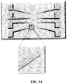
- FIG. 1A shows a schematic diagram of an exemplary device incorporating NMEs.
- the device is a chip having an array of eight leads.
- the NME is formed on gold leads that taper to a width of 5 microns.
- the lead is provided on a substrate of Si and SiCte, although other suitable substrate materials may be used.
- an insulating layer such as Si02, is deposited to electrically insulate and passivate the lead.
- An aperture in this case a 500 nm hole, is created in the insulating layer to expose a portion of the lead.
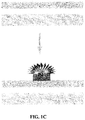
- FIG. IB is a side view of the portion of the chip where the aperture is located, showing the layers of the device.
- Most commonly known photolithography techniques may be suitable for creating an aperture, such as 100 nm to 1 ⁇ m diameter apertures. This is typically achievable in existing fabrication facilities with high robustness and reproducibility. Given that only this exposed surface is electrochemically active, electrodeposition ( Menke et al. Nature Mater. 2006, 5, 914-919 ) may be used to grow an NME within this space.
- FIG. 1C is a cross-sectional schematic of an example of NME deposition, using Pd for the NME. This process will be described in greater detail below.
- FIG. 2 also illustrates the formation of an NME on a chip.
- small electrodes are provided in situ on a chip, with the position and electrical contacting of the NMEs defined photolithographically.
- this chip is an 8-fold multiplexed passive chip.
- a ⁇ 350 nm thick gold layer is patterned, using conventional photolithography techniques, to connect eight 5- ⁇ m-wide Au leads to large metal pads for connection to off-chip instrumentation.
- a pinhole-free insulating Si02 layer is deposited and patterned to create ⁇ 500 nm openings (e.g., by etching) at the end of each of the Au leads, to expose a section of the lead.
- a metal NME is then plated in this opening using electrodeposition.
- the NME may comprise different conductive materials.
- Some examples of NMEs have been formed as follows, although variations are possible and will be described in greater detail below: Branched fractal Pd NMEs were deposited in an aqueous solution containing 5 mM of H 2 PdCl 4 and 0.5 M of HC10 4 using DC potential amperametry at -250 mV for 15 s. Hemispherical Pd NMEs with nanoscale roughness were deposited in an aqueous solution containing 5 mM of H 2 PdCl 4 and 0.5 M of HC1 using DC potential amperametry at -100 mV for 300 s.
- Smooth hemispherical Pd NMEs were fabricated in the same solution at 0 mV for 300 s.
- Au NMEs were fabricated in a gold bath containing 0.01 M solution of HAuCl4 and 0.5 M H 2 SO 4 at -100mV for 40 seconds.
- Pt NMEs were fabricated in a platinum bath containing 5 mM solution of H2PtCk and 0.5 M H 2 SO 4 at -100 mV for 500 s.
- NME size and morphology can be controlled by varying the metal salt concentration, type and concentration of the supporting electrolyte, and electrodeposition potential and duration.
- FIG. 3 is a schematic of an NME with probes with spacers in the probe monolayer and between the electrode and probe.
- a chemical solution containing a metal cation can be brought into communication with the surface of the NME and a reference electrode.
- the reference electrode may be an NME or a conventional electrode on same lead.
- An electrical bias can be provided between the NME and the reference electrode.
- the chemical solution can then be removed and the electrodes washed.
- a solution containing the probe molecule can then be brought into communication with the surface of the NME.
- the probe molecule may be modified or functionalized so that it binds to the surface of the NME.
- the probe molecule may be functionalized with a thiol, amine, or carboxylate group.
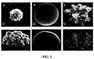
- NMEs with increasing nanostructuring are shown in FIG. 4 .
- variation of electrodeposition conditions allowed growth of extremely smooth hemispherical microelectrodes (left); highly branched nanoscale fractal structures (right); or hemispheres with nanoscale roughness (center).
- the structure on the left was made with HC1 as a supporting electrolyte with an applied potential of 0 mV.
- the center structures were also made with HC1 as a supporting electrolyte but with an applied potential of -100 mV.
- the structure on the right was made with HCIO as a supporting electrolyte and an applied potential of -250 mV.
- the scale bar on the figure corresponds to 5 ⁇ m unless otherwise indicated.
- FIG. 5 illustrates steps involved in the sensing of specific sequences ( Lapierre et al., Anal. Chem. 75:6327 , Ratilainen et al., Biochemistry 39:7781 , Tomlins et al., Science 310:644 )
- Pd NMEs are first modified with thiol-derivatized probe sequences, and then target sequences are hybridized. The presence of the target is then transduced using an electrocatalytic reporter system.
- Electrocatalysis provides electronic amplification, or gain, facilitating high-sensitivity readout: hundreds of electrons may result from each biomolecular complexation event.
- the approach used herein relies on the primary electron acceptor Ru(NH 3 ) 6 3+ , which is electrostatically attracted to the electrode surfaces at levels that are correlated with the amount of bound nucleic acid.
- the inclusion of Fe(CN) 6 3- during electrochemical readout serves to regenerate the Ru(III) substrate, as the Fe(III) species is even easier to reduce, but it is electrostatically repelled from the electrode and thus only undergoes chemical reduction by Ru(II). This method is also label- free and does not require the sample to be processed in any way.
- the biosensing device may be provided in the form of a chip, such as an integrated circuit (IC) chip.
- IC integrated circuit
- an IC incorporating the NME may have a substrate with an electrically conductive lead that is covered by an insulating layer.
- the insulating layer has an aperture that exposes a portion of the lead, and the NME is provided at the exposed portion of the lead.
- the NME is responsive to a biomolecular stimulus.
- the NME may be functionalized with probe molecules that undergo a hybridization reaction with a target biomolecule (e.g., a nucleic acid sequence), resulting in a charge generated at the NME.
- a target biomolecule e.g., a nucleic acid sequence
- the IC also has a charge storage (e.g., a capacitor or a battery) in electrical communication with the lead to store this generated charge.
- a charge storage e.g., a capacitor or a battery
- the NME may be exposed to a sample for a known time duration or an integration period, and the charge stored over that time would then be indicative of the presence and/or amount of the target biomolecule.
- the stored charge may be communicated to a computing device for analysis, or may be displayed (e.g., through a digital display component) for direct reading of the charge stored after the integration period.
- Such an IC may be manufactured using common IC manufacturing equipment, allowing this device to be easily manufactured and to be less costly than other forms of biosensing microelectrodes.
- the materials used may be those already commonly used in IC manufacturing.
- the substrate may be made from silicon, quartz, glass, ceramics, silica, sapphire, gallium arsenide, or other materials currently used for ICs.
- the substrates or supports can incorporate conductive material to serve as an electrode. Conductive supports with a gold surface may also be used.
- the supports usually comprise a flat (planar) surface, or at least a structure in which the probes or p to be interrogated are in approximately the same plane.
- the support can be an electrode, or can be attached to an electrode.
- the lead may be made of Au, Al, W, TiN, polysilicon or other commonly used lead materials.
- the IC may include a transistor, such as a field-effect transistor (FET) including n-type silicon channel FETs and p-type silicon channel FETs, or a bipolar transistor including n-p-n bipolar junction transistors and p-n-p bipolar junction transistors.
- FET field-effect transistor
- bipolar transistor including n-p-n bipolar junction transistors and p-n-p bipolar junction transistors.
- the IC may be provided with, immersed in or otherwise exposed to an electrocatalytic solution in chemical and electrical communication with the NME. This may assist in charge generation in the NME.
- FIG. 6 This figure shows a cross-section of an integrated circuit suited to sensing the presence of biomolecules in a biological sample.
- the substrate (1) is a conventional semiconductor device substrate such as silicon.
- the channel of a transistor (2), a gate oxide (3), and a polysilicon gate electrode (4) are shown to illustrate the use of conventional CMOS electronics to form the integrated circuit's transistors.
- a metal (5) is used to contact the gate electrode.
- a passivation oxide (6) separates the silicon transistor levels below from the top surface of the chip above.
- a series of metal vials (7) and interconnects provide selective paths for electrical communication between the transistor layer and the top electrode(s).
- a substantially planar top surface is a heterogeneous combination of top electrodes (9) and top insulating material (8).
- the figure illustrates an NME (10) provided on the electrode, for example using the methods described above.
- the figure illustrates probe biomolecules (11) such as thiol-terminated nucleic acids that are displayed for efficient hybridization with complementary target molecules.
- An electrocatalytic solution (12) may be employed to provide catalytic read-out of hybridization with the biomolecules (11). Electrical potentials are conveyed, and currents flowed, in a continuous fashion from the NME (10) through the electrical contacts (9) (7) (5) (4) down to the electronic circuitry that resides beneath.
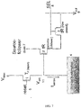
- FIG. 7 showing a circuit diagram of an example circuit that may be used with the disclosed NME.
- the circuit may provide the following functions: biasing of the probe-functionalized NME; integration of the current flowing through the NME into a charge store having a known charge-storage capacity; read-out of the voltage on the charge-store; and selection of the charge-store or NME of interest when a two-dimensional array of stores and electrodes is provided in the context of a highly multiplexed array chip.
- a bias voltage is provided at Vbias; a typical choice of bias may be in the range of about 0.1 - 2.8 V.
- a bias voltage VbiasD is provided at the source-follower drain; a typical choice may be in the range of about 0.1 - 2.8 V.
- a bias voltage VbiasR is provided at the reset node; a typical choice may be an adjustable value between about -2 V and 2.8 V.
- the signal voltages are Vsrc which may typically be in the range of about 1.5 - 2.5 V.
- the column voltage Vcol may be in the range of about 1.5 V - 0.5 V.
- Timing control signals include that for row select (e.g., range may be about 0-2.8 V) and for reset (e.g., range may be about 0-4 V).
- the transistors may be the reset transistor Tr(Reset), the read-out buffer transistor TR(source-follower), and the row-select transistor TR(row-select).
- the probe-functionalized NME may include a NME functionalized using a thiolated nucleic acid probe, for example a probe as described above.
- Vsrc is applied to the probe-functionalized electrode and VbiasR is applied to a second electrode, which may be a NME or any other common electrode, in electrical communication with the electrocatalytic solution.
- VbiasR is applied to a second electrode, which may be a NME or any other common electrode, in electrical communication with the electrocatalytic solution.
- a current may thus flow as a consequence of this potential difference.
- the amount of current flowing may be typically dependent on the amount of hybridization on the probe-functionalized NME, that is the current may be indicative of the amount of target thus detected by the NME.
- the reset transistor is turned on by setting the node 'reset' high enough (e.g., up to 4V, which may be through an on-chip charge-pump or regulator circuit as commonly known in the art) so that node 11 will be charged to a voltage equal to Vbias (node 6) which may be typically set to the supply rail: e.g., 2.8V. This is the reset phase.
- Node 5 may be set to OV to turn off the reset transistor Tr(Reset) (1). In doing so, charge injection and parasitic capacitive feedthrough effects will cause node 11, now becoming a floating node, to drop by approximately 300 mV.
- the current Isense flowing is dependent on the voltage applied (i.e., Vsrc-VbiasR). With VbiasR being able to be set arbitrarily to any voltage level from -2V to 2.8V, the applied potential difference may be adjusted.
- the current Isense discharges the parasitic capacitance at the Vsrc node (11) and its voltage level drops at a rate dependent on the value of the parasitic capacitance at Vsrc (node 11) as well as the flowing Isense during the integration time.
- the resulting integrated voltage at node 11 will be read out through transistors TR(source-follower) and TR(row- select), the source follower buffer transistor and the row-select transistor, by setting the node SEL (8) to a high level (2.8V).
- the charge store that is discharged at node 11 may comprise parasitic capacitance of one or more of the transistors that are in electrical communication with the electrode of the pixel region at Vsrc (node 11).
- the electrode at Vsrc (node 11) may be in electrical communication with the gate of a transistor, such as Tr(source-follower) 2, which provides a parasitic capacitance.
- the charge store may be provided at least in part by a parasitic capacitance between the gate and drain of the source follower transistor, Tr(source-follower) 2, and a parasitic capacitance between the source and substrate of the reset transistor, Tr(Reset) 1.
- parasitic capacitances between the structures on the semiconductor substrate (e.g., the poly, n-well and substrate) on which or in which the pixel circuit is formed.
- these parasitic capacitances may be in the range of about 1-2 femtoFarads or more generally in the range of about 0.5 to 3 femtoFarads or any range subsumed therein.
- the contacts to the probe- functionalized NME may be formed in different layers above the regions of the semiconductor substrate used to form the transistors.
- the polarity of the bias may be reversed and the parasitic capacitance at Vsrc may be charged instead of discharged during the integration period.
- FIG. 8 shows a top view of an example IC that has a multiplexed array of individually-addressable probe-functionalized NMEs.
- individually addressable it is meant that each NME may be individually electrically accessed, such that the current or charge generated by each NME may be individually measured.
- the NMEs are arrayed in a row-column fashion. There are n rows and m columns for a total of m x n independent NMEs. If there were only a single row or column of NME, then it may not be necessary to have row/column address circuitry.
- the charge associated with the current flowing through each NME is integrated into a charge storage, such as a capacitor; and a voltage proportional to the stored charge may be read out for the NME in a particular row by setting the node SEL (8) to a high level and monitoring the voltage on that column Vcol.
- the figure illustrates that, for each column, there may exist a time-dependent signal (whose time-dependence may be determined by the clocking of the row-address circuitry) which, in some embodiments, may be fed, in cases with the aid of electronic buffering or amplification, into an analog-to-digital converter.
- the analog-to-digital converter may accept signals having a pre-determined voltage swing (such as 0-1 V, typically) and, for each input channel, may carry out a quantization operation in which a digital representation of the analog level in that signal is estimated.
- the output of the A/D converter is a digital stream which combines parallelism (e.g., multiple parallel wires, each corresponding to a significant figure in the binary representation of the values) and serial timing (e.g., a timed representation of sequential data elements corresponding, for example, to different probe- fiinctionalized NMEs).
- parallelism e.g., multiple parallel wires, each corresponding to a significant figure in the binary representation of the values
- serial timing e.g., a timed representation of sequential data elements corresponding, for example, to different probe- fiinctionalized NMEs.
- FIG. 9 showing three adjacent NMEs along a single row, in a configuration that may be provided on a biosensing device or IC as described above. These three NMEs are read using three different columns j, j+1, and j+2. This figure illustrates a number of features with respect to the differences among NMEs.
- NMEs Eij and Eij+i may be functionalized both with the same class of probes (e.g. thiolfunctionalized PNA), but the sequences may be different. That is, each NME may be functionalized with similar probes that have different target biomolecules.
- electrodes Eij and Eij+i are response to different sequences present in the sample under study.
- the use of different functionalizations enables sensing of biomolecules within a single class, but having a different sequence, conformation, or functionality.
- NMEs Eij, Eij+i, and Eij+2 are shown having different morphologies and/or sizes, and different degrees of nanostructuring. As discussed above, different morphologies and/or sizes may provide both different limits of detection, and different dynamic ranges, in detecting of target molecules. By incorporating NMEs having different morphologies and/or degrees of nanostructuring onto one device, it may be possible to expand the dynamic range of target concentrations that may be sensed using a single device. In sum, the use of different NME morphologies, sizes and/or nanostructurings may enable sensing of a wider range of concentrations of a given target species than would otherwise be achieved if only one morphology/nanostructuring were provided on a biosensing device.
- NMEs Eij+i and Eij+2 are also depicted as being functionalized using different classes of probe molecules.
- Eij+i may be functionalized using a nucleic acid such as PNA
- Eij+2 may be functionalized using antibodies which attach to the electrode.
- the use of different classes of probe molecules may enable sensing of different classes of target biomolecules, for example ranging from DNA to RNA to micro- RNA to proteins, using a single biosensing device.
- the biosensing device as described above may be incorporated into a biosensing cartridge.
- a biosensing cartridge may contain chambers for sample processing such as disruption and resin or bead-based nucleic acid purification, as well as a chamber for the biosensing device.
- the cartridge may be self-contained, for example all necessary reagents may be contained in the lid of the cartridge.
- the cartridge may be reusable, or may be disposable. A disposable cartridge may minimize the risk of cross-contamination between samples.
- the cartridge may be used in a biosensing workstation for coordinating and carrying out the biosensing process.
- Components of the workstation may include sample holders, instrument tips such as pipettors for manipulation of the sample, a sample identification module, a selection mechanism for selecting a test to be carried out, an electronic display for indicating the results of a biosensing test and a processor for managing these components and carrying out the selected tests.
- the workstation may hold a number of different cartridges at one time (e.g., ten or more).
- the workstation may allow random access to the cartridges - that is, independent tests may be run at any time on any cartridge in the workstation.
- the workstation may have disposable instrument tips, which would be the only part of the workstation that comes into direct contact with the sample and reagents. Disposable tips, together with disposable cartridges, may minimize the risk of cross-contamination between samples tested in the workstation.
- a biosensing cartridge may have a first chamber for containing the sample to be tested, and a second chamber containing the biosensing device as described above.
- the sample may be introduced from the first to the second chamber for detection by the biosensing device in the second chamber.
- the charge or current flow generated in the biosensing device may be measured after an integration period, as described above.
- the cartridge has three chambers, a sample chamber containing the sample, a purifying chamber for purifying the sample, and a biosensing for performing the biosensing.
- the lid of the cartridge is provided with capsules containing reagents for each chamber, and through which an instrument tip may be inserted. This allows the cartridge to be self-contained, already containing the reagents suitable to carry out the biosensing operation and tailored to the particular probes and/or target biomolecules of the biosensing device being used.
- the sample chamber has one capsule, for accessing the sample.
- the purifying chamber has three capsules - two containing a washing reagent, and one containing an elution buffer.
- the biosensing chamber has three capsules - each containing an electrochemical mix containing analytes for the biosensing device.
- the instrument tip may be inserted sequentially in each capsule, in order to carry out the biosensing operation.
- the capsule on the sample chamber may contain a lysis buffer containing chemical dénaturants (e.g., urea or formamide); the capsules one the purifying chamber may have two capsules containing a wash buffer and the elution buffer may be a standard buffer, such as one containing low levels of sodium, chloride and tris salt; the capsules on the biosensing chamber may contain redox reporter groups such as ruthenium hexamine, ferricyanide and a buffer containing sodium, phosphate, chloride and magnesium.
- a lysis buffer containing chemical dénaturants (e.g., urea or formamide)
- the capsules one the purifying chamber may have two capsules containing a wash buffer and the elution buffer may be a standard buffer, such as one containing low levels of sodium, chloride and tris salt
- the capsules on the biosensing chamber may contain redox reporter groups such as ruthenium hexamine, ferricyanide and a buffer containing sodium,
- the sample is first extracted from the sample chamber through its single capsule.
- the sample is then introduced into the purifying chamber, where it is washed twice as the instrument tip is introduced through the two washing capsules and the elution buffer is introduced.
- the sample may be prepared for biosensing by the biosensing device.
- the process in the purifying chamber may isolate the RNA or DNA in the sample.
- the purified sample is then introduced into the biosensing chamber, through each electrochemical capsule.
- the biosensing device in the biosensing chamber may then detect any target biomolecules present in the sample, and the generated current or charge may be measured.
- the processor in the workstation may read this generated current or charge and determine the presence of the target biomolecule based on this reading.
- FIG. 11 showing an example of a biosensing workstation.
- This work station includes a bar code reader, allowing identification of samples using unique bar codes provided on each cartridge.
- the workstation has a selection mechanism, in this example a touch screen that allows the selection of a particular test to be carried out.
- the processor of the workstation may be connected to an external computing device, such as another workstation, for further analysis. This connection may be through a wireless network.
- the workstation may be relatively small (e.g., a footprint of 1.5 x 1 ft), allowing convenience and ease of use.
- a device may be provided with the NME already functionalized with a probe molecule, or the probe molecule may be bound to the NME when preparing the device for use.
- the device is then biased for use, for example by adding an electrocatalytic reporter and waiting a certain time interval.
- a reference electrode which may or may not be an NME, in contact with the electrocatalytic reporter but not in contact with the sample. The current flow or voltage bias generated over this time interval between the NME and the reference electrode may be measured and recorded as the reference point.
- the NME is then exposed to a sample of interest, and the current flow or charge generated over a certain time interval (also referred to as the integration period) may be measured. By comparing the difference in current flow or charge between the exposure time interval and the biasing time interval, the concentration, binding and/or amount of target biomolecule in the sample may be determined.
- sample or “biological sample” as herein refers to any natural (e.g. plant, animal, algal, bacterial or viral) or synthetic material containing DNA, RNA and/or proteins, including, for example, clinical samples, such as tissues, cell cultures or fluids isolated from an individual (including without limitation blood, plasma, serum, cerebrospinal fluid, lymph, tears, urine, saliva, mucus, synovial fluid, cerebrospinal fluid and tissue sections) environment (e.g., water, food or air samples).
- tissue samples including without limitation blood, plasma, serum, cerebrospinal fluid, lymph, tears, urine, saliva, mucus, synovial fluid, cerebrospinal fluid and tissue sections
- environment e.g., water, food or air samples.
- Bio samples may be further processed via a variety of means, including lysis (electrical, mechanical and chemical), electrophoresis, enzymatic digestion. Most often, the sample has been removed from an organism, but the term “biological sample” can also refer to cells or tissue analyzed in vivo, i.e., without removal. Typically, a “biological sample” will contain cells, but the term can also refer to non-cellular biological material, such as non-cellular fractions of blood, saliva, or urine. "A biological sample” further refers to a medium, such as a nutrient broth or gel in which an organism has been propagated, which contains cellular components, such as proteins or nucleic acid molecules.
- Probes for use with the instant described NMEs may be comprised of nucleic acids.
- a "nucleic acid probe” refers to a nucleic acid (e.g. a ribonucleic acid (RNA), deoxyribonucleic acid (DNA) or an analog thereof, including, for example, a peptide nucleic acid (PNA), which contains a backbone comprised of N-(2-aminoethyl)-glycine units linked by peptides rather than deoxyribose or ribose linked by phosphodiesterase linkages) capable of binding to a target nucleic acid of complementary sequence through one or more types of chemical bonds, usually through complementary base pairing, usually through hydrogen bond formation.
- RNA ribonucleic acid
- DNA deoxyribonucleic acid
- PNA peptide nucleic acid
- a nucleic acid probe may include natural (i.e., A, G, C, or T) or modified on bases (7-deazaguanosine, inosine, etc.) or on sugar moiety.
- the bases in a probe can be joined by a linkage other than a phosphodiester bond, so long as it does not interfere with hybridization. It will be understood by one of skill in the art that probes may bind target sequences lacking complete complementarity with the probe sequence depending upon the stringency of the hybridization conditions. By assaying for the presence or absence of the probe, one can detect the presence or absence of the select sequence or subsequence.
- Hybridization refers to any process by which a strand of nucleic acid binds with a complementary strand through base pairing.
- Hybridization conditions refer to standard conditions under which nucleic acid molecules are used to identify similar nucleic acid molecules. Such standard conditions are disclosed, for example, in Sambrook et al., Molecular Cloning: A Laboratory Manual, Cold Spring Harbor Labs Press, 1989 (see specifically, pages 9.31 - 9.62 ).
- formulae to calculate the appropriate hybridization and wash conditions to achieve hybridization permitting varying degrees of mismatch ofnucleotides are disclosed, for example, in Meinkoth et al., 1984, Anal. Biochem. 138, 267-284 .
- Non-limiting examples of hybridization conditions include low stringency hybridization conditions, moderate stringency hybridization conditions and high stringency hybridization conditions.
- the probe is a peptide (comprised of, for example, 4-40 amino acids) or proteins (e.g. antibody) that is able to bind to or otherwise interact with a biomarker target (e.g. receptor or ligand) to provide an indication of the presence of the ligand or receptor in the sample.
- a biomarker target e.g. receptor or ligand
- Probes may include a functional group (e.g., thiol, dithiol, amine, carboxylic acid) that facilitates binding with an NME. Probes may also contain other features, such as longitudinal spacers, double-stranded and/or single-stranded regions, polyT linkers, double stranded duplexes as rigid linkers and PEG spacers.
- a functional group e.g., thiol, dithiol, amine, carboxylic acid
- Probes may also contain other features, such as longitudinal spacers, double-stranded and/or single-stranded regions, polyT linkers, double stranded duplexes as rigid linkers and PEG spacers.
- the surface nanostructure of the NME may be controlled, and may influence the sensitivity and/or efficiency of a device having the NME.
- Example 1 the influence of surface nanostructure on the detection efficiency for nucleic acids was investigated. Two different types of NMEs were compared - a more finely nanostructured NME obtained with a low deposition potential was compared to a more coarsely textured one obtained with a higher deposition potential.
- the 10 aM sensitivity observed here with the disclosed NMEs and electrocataytic reporter system provides a low detection limit for a label- and PCR-ffee sensor; the detection limit corresponds to the detection of ⁇ 100 copies of the target sequence. While the measurement of 60-1000 copies of target sequence has been achieved previously with electrochemical detectors exploiting multi-step catalytic readout ( Munge et al., Anal. Chem. 77 :4662 , Nicewamer-Pena et al., Science 294:137 , Park et al., Science 295 :1503 , Sinensky et al., Nat. Nano. 2 :653 , Steemers et al., Nat. Biotechnol.
- the disclosed device provides this measurement on a chip-based platform with single-step readout.
- Example 2 describes use of a multiplexed electrode platform, as described herein, to directly read a panel of cancer biomarkers in clinically-relevant samples using electronic signals.
- the system combines nanotextured electrodes with rapid catalytic readout to achieve a long-standing goal: the multiplexed analysis of cancer biomarkers using an inexpensive and practical platform.
- Example 3 describes the use of an NME based chip to detect microRNA, one of the most challenging detection targets.
- Electronic readout of microRNA profiles offers a rapid, yet highly accurate, method to directly assay RNA samples for specific sequences without the need for target amplification.
- the provided examples are directed to the detection of cancer biomarkers, other applications may be possible for the NME device, which may involve detecting DNA, RNA and/or proteins.
- Examples include profiling of breast cancer genes (e.g., by detecting RNA markers); profiling of leukemia-related genes (e.g., by detecting RNA markers); profiling of cytochrome P450 mutations that affect drug metabolism (e.g. Warfarin) (e.g., by detecting DNA and RNA markers); profiling of mutations associated with genetic disease (e.g. Cystic fibrosis) (e,g., by detecting DNA markers); detection and typing of viruses (e.g.
- Biosensing devices incorporating these NMEs may be adapted to detect for these other biomolecules by binding suitable probes to the NME and/or by selecting a suitable electrocatalytic reaction to be sensed, as commonly known in the art.
- Pd was used as an electrode material.
- the structures of the Pd NMEs being electrodeposited were monitored as a function of time.
- Time-dependent electrodeposition experiments were performed at -100 mV using 0.5 M HCl as supporting electrolyte.
- Pd structures were formed for (a) 25, (b) 50, (c) 125, (d) 250, and (e) 500 s.
- structures with average diameters of 1.3 ⁇ m and heights of 0.5 ⁇ m were observed, and after 500 s the Pd electrodes were typically 8 ⁇ m and 5 ⁇ m in diameter and height.
- the smaller structures made with shorter deposition times typically exhibited depressions in the center of the microelectrodes, which may indicate that nucleation occurs preferentially at the boundary of the aperture.
- Another controllable parameter that may influence the final structure of the NME is the deposition potential.
- the size and surface morphology of Another controllable parameter that may influence the final structure of the NME is the deposition potential.
- the size and surface morphology of the NMEs may be controlled in this way. Dendritic fractals are phenomena generally observed in non-equilibrium growth such as the growth of snowflakes, the aggregation of soot particles, and the solidification of metals. Such fractal structures are also obtained by nonequilibrium electrodeposition of metals and used as model systems for the study of branching and fractal growth processes ( Fleury, Nature 1997, 390, 145-148 ).
- the electrochemical behaviour of the Pd NMEs formed as a function of potential was studied by cyclic voltammetry (CV).
- the electrochemical response of the NMEs was monitored in a solution containing 3 mM Ru(NH3)6 3+ and 0.09 M sodium phosphate, at a scan rate of 100 mV/s.
- steady-state voltammograms are observed for each electrode, consistent with the microscale dimensions of the electrodes.
- the currents observed are well- correlated with the size of the electrode. That is, the greater the diameter of the NME (i.e., formed at a larger applied potential), the greater the response current observed.
- currents observed were lower than expected based on the size of the microelectrode, indicating that the discontinuity of the electrode structure may lead to poor electrical connectivity and loss of working area.
- moderate deposition potentials appear to provide the most pronounced nanotexturing while maintaining the integrity of the resultant NME, as small nanoparticles are formed on the surface of the microelectrodes. It appears that providing too large of a driving potential for the deposition reaction accelerates the kinetics to a point where metal nanoparticles are formed without strong connectivity to the core of the NME.
- NME morphology may also be controlled via electrolyte effects.
- Pd NMEs were formed at -100 mV for 250s using (a) 0.5M H2SO4 and (b) 0.5M HCIO4 as the supporting electrolyte. These structures were formed under the same conditions as described above, where HC1 was used as a supporting electrolyte. The structures formed in H2SO4 and HC1O4 were significantly larger than those formed in HC1, and interestingly, all three displayed different types of nanostructuring. NMEs made in HCIO4 showed the finest nanostructuring, with features as small as 10-20 nm present. In HC1, the electrode was more compact, and the nanostructuring was on the order of 100 nm. The coarsest nanostructuring was obtained in H2SO4, where the particles comprising the electrode were larger than 200 nm. These observations indicate that the NME morphology may also be controlled by varying the supporting electrolyte used for electrodeposition.
- the dendritic structures for the NME depend on the conditions during manufacture, including concentrations of the electrodeposition solution, choice of the metal to be electrodeposited, and the applied potential during electrodeposition. These parameters are readily controllable. For example, it may be desirable to control the concentration and purity of the reagents used in electrodeposition to within 5%. The choice of metal is simple to control as long as purity of the reagents is high, simply by obtaining the correct material. The potential during electrodeposition may be readily controlled to within a few mV, which is sufficient for controlling the size and morphology of the resultant NME.
- Chip fabrication The chips were fabricated at the Canadian Photonics Fabrication Center. 3" silicon wafers were passivated using a thick layer of thermally grown silicon dioxide. A 350 nm gold layer was deposited on the chip using electron-beam assisted gold evaporation. The gold film was patterned using standard photolithography and a lift-off process. A 500 nm layer of insulating silicon dioxide was deposited using chemical vapor deposition. 500 nm apertures were imprinted on the electrodes using standard photolithography, and 2 mm x 2 mm bond pads were exposed using standard photolithography.
- Chips were cleaned by rinsing in acetone, IP A, and DI water for 30 s and dried with a flow of nitrogen. All electrodeposition was performed at room temperature with a Bioanalytical Systems Epsilon potentiostat with a three-electrode system featuring an Ag/AgCl reference electrode and a platinum wire auxiliary electrode. 500 nm apertures on the fabricated electrodes were used as the working electrode and were contacted using the exposed bond pads. Platinum NMEs were fabricated in a platinum bath containing 5 mM solution of H2PtC16 and 0.5 M HC104 at -250 mV for 10 s using DC potential amperometry.
- oligonucleotides Preparation and purification of oligonucleotides. All synthetic oligonucleotides were stringently purified by reversed-phase HPLC. The following probe and target sequences were used in experiments. Seq. PI. Type III fusion probe (PNA): NH2-Cys-Gly- ATA AGG CTT CCT GCC GCG CT-CONH2 (SEQ ID NO. 1), Seq. P2. Type I fusion probe (PNA): NH2-Cys-Gly-CTG GAA TAA CCT GCC GCG CT-CONH2 (SEQ ID NO. 2), Seq. P3.
- PNA Type III fusion probe
- Type I fusion probe PNA
- SEQ ID NO. 2 Seq. P3.
- Type VI fusion probe PNA: NH2-Cys-Gly-ATA AGG CTT CTG AGT TCA AA-CONH2 (SEQ ID NO. 3), Seq. T1 (Type III TMPRSS2:ERG fusion DNA target): 5'AGC GCC GCA GGA AGC CTT AT3' (SEQ ID NO. 4), Seq. T2 (WT TMPRSS2 DNA target): 5'AGC GCC GCC GGT CAT 10 ATT GA3' (SEQ ID NO. 5), Seq. T3 (WT ERG DNA target): 5'TCA TAT CAA GGA AGC CTT AT3' (SEQ ID NO. 6), Seq.
- PNA Type VI fusion probe
- T4 noncomplementary DNA target: 5'TTT TTT TTT TTT TTT TTT TT3' (SEQ ID NO. 7). Oligonucleotides were quantitated by measuring absorbance at 260 nm and ext. coefficients calculated using: http://www.idtdna.com/analyzer/Applications/01igoAnalyzer/.
- NMEs Modification of NMEs with PNA probes.
- a solution containing 500 nM thiolated single stranded PNA, 25 mM sodium phosphate (pH 7), and 25 mM sodium chloride was heated at 50°C for 10 minutes.
- a suitable amount of 10 mM MCH was then added to make the final MCH concentration of 100 nM.
- 0.5-10 ⁇ L (depending on the degree of multiplexing) of this mixture was deposited on the NMEs in a dark humidity chamber overnight at 4°C.
- the NMEs were rinsed in 25 mM sodium phosphate (pH 7), and 25 mM NaCl buffer before measurement.
- Electrochemical measurements Electrochemical signals were measured in solutions containing 10 ⁇ M Ru(NH 3 ) 6 3+ , 25 mM sodium phosphate (pH 7), 25 mM sodium chloride, and 4 mM Fe(CN) 6 3- .
- Differential pulse voltammetry (DPV) signals before and after hybridization were measured using a potential step of 5 mV, pulse amplitude of 50 mV, pulse width of 50 ms, and a pulse period of 100 ms. Cyclic voltammetry signals before and after hybridization were collected with a scan rate of 100 mV/s.
- Hybridization protocol Hybridization solutions typically contained target sequences in 25 mM sodium phosphate (pH 7), and 25 mM NaCl. Electrodes were incubated at 37°C in humidity chamber in dark for 60 minutes and were washed extensively with buffer before electrochemical analysis.
- mRNAs were extracted from cell lines and patient tissue samples with the Dynabeads mRNA Direct Kit (Invitrogen). Two typical prostate cancer tissue samples were obtained from radical prostatectomies collected by from the Cooperative Human Tissue Network. The tissue was stored at -85°C until tumor-rich tissue was selected for mRNA extraction, The concentrations of mRNA targets were measured by NanoDrop ND-1000 of Thermo Fisher Scientific (USA). All of the fusion sequences were confirmed by RT-PCR and direct sequencing.
- the surfaces of the microelectrodes displayed a high level of nanostructuring, with feature sizes of approximately 20 nm. These structures displayed ideal microelectrode behavior, exhibiting low capacitive currents and high steady-state plateau currents.
- NMEs nanostructured microelectrodes
- PNA thiolated peptide-nucleic acids
- This reporter system relies on the accumulation of Ru(NH3)63+ at electrode surfaces when polyanionic species like nucleic acids bind, and the catalysis of the reduction of Ru(III) via the inclusion of Fe(CN)63-, which regenerates Ru(III) and allows multiple reductions per metal center.
- PNA-modified NMEs were challenged with a complementary sequence, detectable signal changes could be clearly detected through the femtomolar concentration range. Negligible signal changes were observed with completely non-complementary sequences.
- the cancer biomarkers selected for analysis on this platform are a group of gene fusions specific to prostate cancer. These fusions, resulting from a chromosomal translocation that joins the ERG and TMPRSS2 genes, were recently discovered and appear in at least 50% of prostate tumours. Furthermore, there are ⁇ 20 sequence types that feature different fusion sites, and the exact type of fusion present in a tumour appears to correlate with its aggressiveness and metastatic potential. These sequences are therefore not only promising diagnostic markers, but are also factors with prognostic value.
- a sensor modified with a probe complementary to the splice site of the Type III fusion was challenged with: (1) the fusion target (seq. T1), (2) the sequence corresponding to the wild-type TMPRSS2 gene (seq. T2), and (3) a sequence corresponding to the wild-type ERG gene (seq. T3).
- a completely non-complementary control was also assayed (seq. T4). With a hybridization time of 60 minutes, large signal increases were observed with the fully complementary target, while a much lower signal change was seen with the TMPRSS2 target.
- the ERG target produced an even lower signal change, and that observed with the non-complementary sequence was negligible.
- the TMPRSS2 target binds to the portion of the probe located at the end of the sequence not attached to the electrode, while the ERG target binds to the portion of the probe located at the end tethered to the electrode surface.
- the different signal levels observed indicate that the most accessible side of the probe is better able to bind incoming target molecules, while hybridization with the more buried part of the sequence is inefficient.
- the electrocatalytic signals were monitored at a variety of intervals within the window originally tested. Interestingly, the rise of the signals is very fast, with significant current changes observed within 2 minutes. Over the total 60-minute period, however, the signals for the half-complementary and non- complementary sequences fall noticeably; with 20-50% of the 2-minute signal vanishing by 60 minutes. It appears that for sequences that are not fully complementary, some nonspecific binding occurs in the first few minutes of exposure of the NME sensor to the target solution, but these complexes do not remain stable and do not remain immobilized on the electrode. Thus, while non-complementary sequences can be discriminated from complementary sequences with short hybridization times, longer times increase the differential signal changes, and thus the degree of specificity.
- the ultimate application of the NME chip is the direct, multiplexed analysis of a panel of cancer biomarkers in relevant patient samples.
- a panel of mRNA samples collected from cell lines and clinical tumor samples for a series of gene fusions.
- type III fusions being the most common but correlating with low cancer recurrence rates
- type I and VI fusions are correlated with aggressive cancers with high levels of recurrence. It is therefore of great interest to be able to differentiate these fusions in tumours, and a method that would permit their presence or absence to be assessed quickly and straightforwardly would be of value in their further study and validation as diagnostic biomarkers.
- Probes complementary to each of the three fusions were deposited on their respective electrodes on NME chips, and 5 different mRNA samples were profiled for the presence of different gene fusions in a multiplexed format. Three cell lines were tested: VCap (type III positive),28 NCI-H660 (type III and VI positive)30, and DU145 (fusion negative).28 In addition, two tumour samples (tissues collected by radical prostatectomies) were tested, one that was positive for the type I fusion, and one that was positive for the type III fusion, as confirmed by conventional sequencing. In each case, all experiments took less than 2 hours and required only 10 ng of mRNA.
- the detection platform described here is not only specific, sensitive, and robust, it is also practical and scalable.
- the reproducible fabrication method we chose is amenable to the production of probe-modified chips using the same photolithographic technologies in widespread use in consumer electronics microchip fabrication; and only simple, inexpensive instrumentation is needed for readout.
- Microfluidics are not required for automated analysis, as hybridization can be performed and read out in a single reaction vessel. This system represents an attractive alternative to PCR-based methods that are sensitive but difficult to automate in a clinical setting.
- the new multiplexed electrode platform we describe here is the first to read directly a panel of cancer biomarkers in clinically-relevant samples using electronic signals.
- the array enabling these measurements features microelectrodes that possess controllable and versatile nanotexturing essential for sensitivity.
- the system combines these nanotextured electrodes with rapid catalytic readout to achieve a long-standing goal: the multiplexed analysis of cancer biomarkers using an inexpensive and practical platform.
- Example 3 Direct, Electronic MicroRNA Detection Reveals Differential Expression Profiles in 30 Minutes.
- 6-mercapto-1-hexanol (97% MCH), hexaamine ruthenium chloride (99.9+%), potassium ferricyanide (99%), and palladium (II) chloride(99.9+%) were purchased from Sigma-Aldrich Canada Ltd (Oakville, ON), perchloric acid (70%), acetone (ACS grade) and isopropyl alcohol (IPA, ACS grade) were obtained from EMD (Gibbstown, NJ).
- Thiolated PNA oligomers were obtained from Biosynthesis Inc (Lewisville, TX) with HPLC purified grade. PNA probes a Cys-Gly dipeptide at their N- terminus.
- Synthetic microRNAs (5' end phosphorylated and HPLC purified) were obtained from Eurofins MWG Operon (Huntsville, AL). All PNA and RNA sequences are shown in table SI provided in the supporting information.
- Chip fabrication The chips were fabricated at the Canadian Photonics Fabrication Center. 3" silicon wafers were passivated using a thick layer of thermally grown silicon dioxide. A 350 nm gold layer was deposited on the chip using electron-beam assisted gold evaporation. The gold film was patterned using standard photolithography and a lift-off process. A 500 nm layer of insulating silicon dioxide was deposited using chemical vapor deposition. 500 nm apertures were imprinted on the electrodes using standard photolithography, and 2 mm x 2 mm bond pads were exposed using standard photolithography.
- Chips were cleaned by rinsing in acetone, IPA, and DI water for 30 s and dried with a flow of nitrogen. All electrodeposition was performed at room temperature with a Bioanalytical Systems Epsilon potentiostat with a three-electrode system featuring an Ag/AgCl reference electrode and a platinum wire auxiliary electrode. 500 nm apertures on the fabricated electrodes were used as the working electrode and were contacted using the exposed bond pads. A 2 mm portion of the chip was immersed into the plating bath containing 5 mM palladium (II) chloride and 0.5 M perchloric acid, and incubated for about 5 min prior to electroplating. The bond pads were kept free from solution. Pd NMEs were fabricated using DC potential amperometry at an applied potential of -100 mV for 6 s.
- Hybridization solutions contained various concentrations of targets in 25 mM sodium phosphate (pH 7.0) and 25 mM NaCl. Pd NMEs were incubated with 10 ⁇ L of target solution at 37°C in a humidity chamber for 30 mins to allow the immobilized probe molecules to hybridize with target molecules. The chip was then cooled and washed vigorously with buffer before the electrochemical analysis.
- Electrochemical measurements were performed with an electrochemical analyzer (BASi, West Lafayette, USA) in a solution containing 10 mM Ru(NH3)6 3+, 4 mM Fe(CN)6 3-, 25 mM sodium phosphate (pH 7.0) and 25 mM NaCl. Cyclic voltammetry (CV) was conducted before and after the addition of target solutions at a scan rate of 100 mV/s. Differential pulse voltammetry (DPV) was performed at a potential step of 5 mV, pulse amplitude of 50 mV, pulse width of 50 ms and a pulse period of 100 ms. Cyclic voltammetry signals before and after hybridization were collected with a scan rate of 100 mV/s.
- HITACHI S-3400 SEM (Hitachi High Technologies America, Inc., Pleasanton, CA) was employed to study the morphology and dimension of the electroplated NMEs.
- the chip was affixed on a stainless steel SEM stub using doublesided adhesive black carbon tape.
- the SEM image was acquired using the secondary electron mode at 20 kV.
- RNA extraction for PCR analyses and amplification protocol.
- Total RNA was extracted from cell lines with mirVana kit (Ambion). The quality of samples was assessed by RT-PCR analysis of the endogenous control RNU44 using Applied Biosystems TaqMan® microRNA Assay.
- This assay includes a reverse transcription (RT) step using the TaqMan® MicroRNA Reverse Transcription Kit (Applied Biosystems, CA, USA) wherein a stemloop RT primer specifically hybridizes to a mir molecule and is then reverse transcribed with a MultiScribe reverse transcriptase.
- RT reverse transcription
- the reverse transcription mix includes 50 nM stem-loop RT primers, 1x RT buffer, 0.25 mM each of dNTPs, 3.33 U/ ⁇ L MultiScribe reverse transcriptase, and 0.25 U/ ⁇ l RNase inhibitor.
- the 7.5 ⁇ L reaction was then incubated in an Applied Biosystems 7900 Thermocycler for 30 minutes at 16°C, 30 minutes at 42°C, 5 minutes at 85°C and then held at 4°C.
- the RT products were subsequently amplified with sequence-specific primers (hsa-mir-21 primer 4373090, and hsa-mir-205 primer 4373093 from Applied Biosystems) using the Applied Biosystems 7900 HT Real-Time PCR system.
- the 10 ⁇ L PCR mix contains 0.67 ⁇ L RT product, 1x4 TaqMan® Universal PCR Master Mix, 0.2 ⁇ M TaqMan® probe, 1.5 ⁇ M forward primer and 0.7 ⁇ M reverse primer.
- the reactions were incubated in a 384-well plate at 95°C for 10 minutes followed by 40 cycles of 95°C for 15 seconds and 60°C for 1 minute.
- cDNA was produced by reverse transcribing 500 ng total RNA from FaDu cells using High-Capacity cDNA Reverse Transcription Kit (Applied Biosystems) according to manufacturer's instructions. 50 ng of cDNA were used as template for PCR amplification of the premiRNA-21 stem loop with 1 HM of the primers MIR-F (CCT ACC ATC GTG AC A TCT CCA TGG) and MIR-R (ATG AGA ACA TTG GAT ATG GAT GAT GGT).
- MIR-F CCT ACC ATC GTG AC A TCT CCA TGG
- MIR-R ATG AGA ACA TTG GAT ATG GAT GAT GAT GGT
- the conditions for the PCR were: 95°C for 2 min, followed by 40 cycles of 95°C for 1 min, 55°C for 1 min, and 72°C for 1 min, and a final extension step at 72°C for 10 min.
- the PCR product was gel purified (Gel extraction kit, Qiagen) and cloned in pCR4-TOPO vector (invitrogen). Colonies were picked and grown in LB medium. Plasmid DNA was purified with Plasmid Mini Kit (Qiagen), and checked for the correct product, orientation, and absence of undesired mutations with sequencing (ACGT corporation). Plasmid DNA was digested with Not1 which does not generate 3' protruding ends that produce high background vector RNA during in vitro transcription.
- a multiplexed chip was prepared that featured an electrode pattern generated by photolithography. This chip was made using a silicon wafer as a base, and a pattern of gold was deposited on its surface to provide a multiplexed set of leads and external contacts. A layer of SiO was deposited on top of the gold to passivate the metal, and then in the final fabrication step, 500 nanometer apertures were opened on the end of each lead to expose gold. To generate protruding micorelectrodes, palladium was electrodeposited in the apertures. The electrodeposition step was engineered to produce highly nanostructured microelectrodes (NMEs). Previous studies have indicated that nanostructured sensing elements can present biomolecular probes more efficiently than bulk materials and facilitate surface complexation reactions, but this advantage has never been exploited for direct biological profiling.
- NMEs nanostructured microelectrodes
- RNA samples extracted from human normal cells and those derived from human head and neck squamous cancer cell lines grown in culture For example, total RNA extracted from the human hypopharyngeal squamous cancer FaDu cell line and a normal oral epithelial cell line was titrated onto a nanostructured microelectrode displaying a probe complementary to miR -205.
- RNA derived from the FaDu cells A positive signal was obtained with as little as 5 ng of RNA derived from the FaDu cells, while normal epithelial cells did not produce any signal change with up to 20 ng of RNA. This indicates that the signal response corresponds to a unique marker present at significantly higher levels in the cancer cell lines.
- RNA samples were profiled two different microRNAs, miR-21 and miR-205, and also included a control RNA, RNU-44 in a panel of total RNA samples.
- RNU -44 levels as judged by the electrochemical response measured for each total RNA sample exposed to a sensing element modified with a complementary probe, remained constant in all four cell lines.
- miR-21 and miR-205 signals were both significantly elevated in the cancer cell lines.
- microRNA detection chip described here offers the sensitivity and specificity for the analysis of a novel class of nucleic acids biomarkers representing one of the most challenging detection targets.
- Electronic readout of microRNA profiles offers a rapid - yet highly accurate - method to directly assay RNA samples for specific sequences, and the lack of labeling or amplification renders this approach to be extremely straightforward and efficient, features not attainable with other PCR or hybridization-based approaches.
Claims (15)
- Bioerfassungsvorrichtung, die Folgendes umfasst:ein Substrat;mindestens eine elektrisch leitfähige Leitung auf dem Substrat;eine Isolierschicht, die die Leitung bedeckt, wobei die Isolierschicht eine Öffnung aufweist, die einen Raum definiert, in dem ein Abschnitt der Leitung freigelegt ist; undeine nanostrukturierte Mikroelektrode, die innerhalb der Öffnung gelagert ist, wobei die Mikroelektrode durch Mittel eines elektrokatalytischen Reportersystems angepasst ist, eine Ladung als Antwort auf einen biomolekularen Stimulus zu erzeugen, wobei:die nanostrukturierte Mikroelektrode fähig ist, eine biomolekulare Sonde an der Oberfläche davon zu präsentieren, unddie nanostrukturierte Mikroelektrode in elektrischem Kontakt mit dem freigelegten Abschnitt der Leitung steht.
- Vorrichtung nach Anspruch 1, wobei eine Vielzahl von Mikroelektroden in einer Anordnung bereitgestellt ist, und wobei jede Mikroelektrode einzeln adressierbar ist.
- Verfahren zum Herstellen einer Bioerfassungsvorrichtung, wobei das Verfahren Folgendes umfasst:Bereitstellen eines Substrats und einer elektrisch leitfähigen Leitung auf dem Substrat, wobei die Leitung durch eine Isolierschicht bedeckt ist;Ätzen einer Öffnung in die Isolierschicht, um einen Abschnitt der Leitung freizulegen; undgalvanisches Abscheiden eines leitfähigen Materials auf den freigelegten Abschnitt der Leitung, um eine nanostrukturierte Mikroelektrode zu bilden.
- Verfahren nach Anspruch 3, wobei das galvanische Abscheiden das Steuern eines angelegten Potentials umfasst, um eine Morphologie zu erreichen, die aus der Gruppe ausgewählt ist, die Folgendes umfasst: halbkugelförmig, unregelmäßig, zyklisch oder fraktal.
- Verfahren nach Anspruch 4, wobei die Morphologie der fraktalen nanostrukturierten Mikroelektrode dendritisch ist.
- Verfahren nach einem der Ansprüche 3 bis 5, wobei der geätzte Bereich photolithographisch definiert ist.
- Verfahren nach Anspruch 3, wobei eine Vielzahl von elektrisch leitfähigen Leitungen auf dem Substrat bereitgestellt ist, und wobei das Verfahren ferner das Ätzen einer Öffnung in die Isolierschicht umfasst, um einen Abschnitt jeder Leitung freizulegen und ein leitfähiges Material auf den freigelegten Abschnitt jeder Leitung galvanisch abzuscheiden, um eine Vielzahl von einzeln adressierbaren nanostrukturierten Mikroelektroden zu bilden.
- Verfahren nach Anspruch 7, wobei jede der Vielzahl von einzeln adressierbaren nanostrukturierten Mikroelektroden unterschiedliche leitfähige Materialien, Morphologien, Größen, und/oder Nanostrukturierung umfasst.
- Verfahren nach Anspruch 7 oder 8, wobei die nanostrukturierten Mikroelektroden unter Verwendung derselben Klasse von Sondenmolekülen, die unterschiedliche Sequenzen aufweisen, funktionalisiert sind.
- Verfahren nach Anspruch 7 oder 8, wobei die nanostrukturierten Mikroelektroden unter Verwendung von unterschiedlichen Klassen von Sondenmolekülen funktionalisiert sind.
- Bioerfassungskartusche, die eine Probenkammer zum Aufnehmen einer biologischen Probe und eine Bioerfassungskammer zum Aufnehmen der Bioerfassungsvorrichtung nach Anspruch 1 oder 2 umfasst.
- Kartusche nach Anspruch 11, wobei die Kartusche angepasst ist, die biologische Probe durch chemische, mechanische oder Vibrationsmittel zu unterteilen.
- Verfahren zum Ausführen eines Bioerfassungsprozesses unter Verwendung einer nanostrukturierten Mikroelektrode, wobei das Verfahren Folgendes umfasst:Bereitstellen der Bioerfassungsvorrichtung nach Anspruch 1;Vorspannen der Mikroelektrode relativ zu einer Referenzelektrode;Messen einer Referenzladung oder eines Referenzstromflusses zwischen der Mikroelektrode und der Referenzelektrode;Aussetzen der Mikroelektrode an einen biomolekularen Stimulus;Messen einer Ladung oder eines Stromflusses, die bzw. der an der Mikroelektrode als Antwort auf den biomolekularen Stimulus erzeugt wurde, durch Mittel des elektrokatalytischen Reportersystems; undBestimmen der Menge von biomolekularem Stimulus durch Vergleichen der gemessenen Ladung oder des gemessenen Stromflusses mit der Referenzladung oder dem Referenzstromfluss.
- Verfahren nach Anspruch 13, wobei eine Vielzahl von nanostrukturierten Mikroelektroden in einer Anordnung bereitgestellt ist, und wobei jede nanostrukturierte Mikroelektrode einzeln adressierbar ist.
- Verfahren nach Anspruch 14, wobei die Anordnung zur Multiplex-Analyse von Krebsbiomarkern in biologischen Proben verwendet wird.
Priority Applications (1)
| Application Number | Priority Date | Filing Date | Title |
|---|---|---|---|
| EP17165963.4A EP3279651B1 (de) | 2008-09-02 | 2009-09-01 | Vefahren zur nutzung nanostrukturierter mikroelektroden |
Applications Claiming Priority (2)
| Application Number | Priority Date | Filing Date | Title |
|---|---|---|---|
| US9366708P | 2008-09-02 | 2008-09-02 | |
| EP09810953.1A EP2331950B1 (de) | 2008-09-02 | 2009-09-01 | Nanostrukturierte mikroelektroden und bioerfassungsvorrichtungen damit |
Related Parent Applications (1)
| Application Number | Title | Priority Date | Filing Date |
|---|---|---|---|
| EP09810953.1A Division EP2331950B1 (de) | 2008-09-02 | 2009-09-01 | Nanostrukturierte mikroelektroden und bioerfassungsvorrichtungen damit |
Related Child Applications (1)
| Application Number | Title | Priority Date | Filing Date |
|---|---|---|---|
| EP17165963.4A Division EP3279651B1 (de) | 2008-09-02 | 2009-09-01 | Vefahren zur nutzung nanostrukturierter mikroelektroden |
Publications (2)
| Publication Number | Publication Date |
|---|---|
| EP2803988A1 EP2803988A1 (de) | 2014-11-19 |
| EP2803988B1 true EP2803988B1 (de) | 2017-04-12 |
Family
ID=41796674
Family Applications (3)
| Application Number | Title | Priority Date | Filing Date |
|---|---|---|---|
| EP09810953.1A Not-in-force EP2331950B1 (de) | 2008-09-02 | 2009-09-01 | Nanostrukturierte mikroelektroden und bioerfassungsvorrichtungen damit |
| EP17165963.4A Not-in-force EP3279651B1 (de) | 2008-09-02 | 2009-09-01 | Vefahren zur nutzung nanostrukturierter mikroelektroden |
| EP14176968.7A Not-in-force EP2803988B1 (de) | 2008-09-02 | 2009-09-01 | Nanostrukturierte Mikroelektroden und Bioerfassungsvorrichtungen damit |
Family Applications Before (2)
| Application Number | Title | Priority Date | Filing Date |
|---|---|---|---|
| EP09810953.1A Not-in-force EP2331950B1 (de) | 2008-09-02 | 2009-09-01 | Nanostrukturierte mikroelektroden und bioerfassungsvorrichtungen damit |
| EP17165963.4A Not-in-force EP3279651B1 (de) | 2008-09-02 | 2009-09-01 | Vefahren zur nutzung nanostrukturierter mikroelektroden |
Country Status (8)
| Country | Link |
|---|---|
| US (3) | US8888969B2 (de) |
| EP (3) | EP2331950B1 (de) |
| JP (4) | JP5712129B2 (de) |
| CN (2) | CN102216762B (de) |
| CA (1) | CA2735735C (de) |
| ES (3) | ES2517919T3 (de) |
| HK (2) | HK1163247A1 (de) |
| WO (1) | WO2010025547A1 (de) |
Families Citing this family (81)
| Publication number | Priority date | Publication date | Assignee | Title |
|---|---|---|---|---|
| CN102216762B (zh) | 2008-09-02 | 2016-02-10 | 多伦多大学董事局 | 纳米结构的微电极以及集成所述微电极的生物传感器件 |
| JP5586001B2 (ja) * | 2009-08-26 | 2014-09-10 | 独立行政法人物質・材料研究機構 | ナノリボン及びその製造方法、ナノリボンを用いたfet及びその製造方法、ナノリボンを用いた塩基配列決定方法およびその装置 |
| CA2798123C (en) | 2010-05-05 | 2020-06-23 | The Governing Council Of The University Of Toronto | Method of processing dried samples using digital microfluidic device |
| US20130240376A1 (en) | 2010-09-02 | 2013-09-19 | Heed Diagnostics Aps | Electrochemical detection of analyte |
| EP2663857B1 (de) | 2011-01-11 | 2018-12-12 | The Governing Council Of The University Of Toronto | Proteinnachweisverfahren |
| WO2012109157A2 (en) * | 2011-02-07 | 2012-08-16 | The Governing Council Of The University Of Toronto | Bioprobes and methods of use thereof |
| WO2012122564A2 (en) | 2011-03-10 | 2012-09-13 | Xagenic, Inc. | Diagnostic and sample preparation devices and methods |
| CA2856881A1 (en) * | 2011-11-23 | 2013-05-30 | The Governing Council Of The University Of Toronto | Versatile and sensitive biosensor |
| US8858778B2 (en) * | 2012-01-19 | 2014-10-14 | Michael James Darling | Method for DNA defined etching of a graphene nanostructure |
| WO2013126906A1 (en) * | 2012-02-24 | 2013-08-29 | University Of Washington Through Its Center For Commercialization | Method and system for concentrating particles from a solution |
| WO2013176773A1 (en) * | 2012-05-24 | 2013-11-28 | The Governing Council Of The University Of Toronto | Systems and methods for multiplexed electrochemical detection |
| JP6340002B2 (ja) * | 2012-07-02 | 2018-06-06 | コーニンクレッカ フィリップス エヌ ヴェKoninklijke Philips N.V. | バリアコーティングされたナノ構造体 |
| US20140027314A1 (en) * | 2012-07-24 | 2014-01-30 | Snu R&Db Foundation | Binding enhancing apparatus, method of binding enhancion using the same and biosensor, biosensor array and sensing method using the same |
| CA2884531A1 (en) * | 2012-09-12 | 2014-03-20 | Xagenic Inc. | Systems, devices, and methods for identifying a disease state in a biological host using internal controls |
| WO2014052618A1 (en) * | 2012-09-26 | 2014-04-03 | Advanced Diamond Technologies, Inc. | Conductive nanocrystalline diamond micro-electrode sensors and arrays for in-vivo chemical sensing of neurotransmitters and neuroactive substances and method of fabrication thereof |
| ITMI20121909A1 (it) * | 2012-11-09 | 2014-05-10 | Industrie De Nora Spa | Cella elettrolitica dotata di microelettrodi |
| US9850520B2 (en) * | 2013-07-03 | 2017-12-26 | Kansas State University Research Foundation | Electrochemical detection of proteases using AC voltammetry on nanoelectrode arrays |
| CN103412000B (zh) * | 2013-07-29 | 2015-08-19 | 浙江大学 | 一种ZnO/NiO单根弯曲纳米线异质结生物传感器及制备方法 |
| EP3030699A4 (de) * | 2013-08-07 | 2017-07-26 | Xagenic, Inc. | Sensorwachstumssteuerung |
| US10416109B2 (en) | 2013-08-07 | 2019-09-17 | General Atomics | Microchip structure and treatments for electrochemical detection |
| CN105849032B (zh) * | 2013-10-23 | 2018-08-07 | 多伦多大学董事局 | 打印式数字微流体装置的使用及其制造方法 |
| US10253353B2 (en) * | 2013-12-06 | 2019-04-09 | The Broad Institute, Inc. | Enhanced methods of ribonucleic acid hybridization |
| US10856764B2 (en) | 2014-08-07 | 2020-12-08 | The Regents Of The University Of California | Method for forming a multielectrode conformal penetrating array |
| CN104391017B (zh) * | 2014-08-20 | 2016-07-13 | 湖北民族学院 | 一种传感器及其制备方法 |
| EP3213067A4 (de) * | 2014-10-28 | 2018-05-30 | The Governing Council Of The University Of Toronto | Vorrichtung für den nachweis der elektrochemischen stoffwechselaktivität |
| CN104406881B (zh) * | 2014-11-18 | 2017-09-26 | 中国科学院苏州生物医学工程技术研究所 | 一种基于微纳结构的压电声波生物传感器 |
| US20160265064A1 (en) * | 2015-03-11 | 2016-09-15 | The Governing Council Of The University Of Toronto | Electrochemical clamp assay |
| US20160281147A1 (en) * | 2015-03-26 | 2016-09-29 | Xagenic Inc. | Ultrasensitive diagnostic device using electrocatalytic fluid displacement (efd) for visual readout |
| EP3303547A4 (de) | 2015-06-05 | 2018-12-19 | Miroculus Inc. | Vorrichtung und verfahren für digitale luftmatrix-mikrofluidik zur begrenzung der verdampfung und oberflächenverunreinigung |
| US10695762B2 (en) | 2015-06-05 | 2020-06-30 | Miroculus Inc. | Evaporation management in digital microfluidic devices |
| WO2017007826A1 (en) * | 2015-07-06 | 2017-01-12 | Georgia State University Research Foundation, Inc. | Systems for detecting and quantifying nucleic acids |
| JP6086412B1 (ja) * | 2015-12-22 | 2017-03-01 | 日本航空電子工業株式会社 | 電気化学測定方法、電気化学測定装置及びトランスデューサ |
| US11624725B2 (en) | 2016-01-28 | 2023-04-11 | Roswell Blotechnologies, Inc. | Methods and apparatus for measuring analytes using polymerase in large scale molecular electronics sensor arrays |
| JP7080489B2 (ja) | 2016-01-28 | 2022-06-06 | ロズウェル バイオテクノロジーズ,インコーポレイテッド | 超パラレルdna配列決定装置 |
| CN105606673A (zh) * | 2016-02-03 | 2016-05-25 | 北京大学 | 一种可用于电化学实时pcr的芯片及其制备方法 |
| CA3053103A1 (en) | 2016-02-09 | 2017-08-17 | Roswell Biotechnologies, Inc. | Electronic label-free dna and genome sequencing |
| US10597767B2 (en) | 2016-02-22 | 2020-03-24 | Roswell Biotechnologies, Inc. | Nanoparticle fabrication |
| WO2017219771A1 (zh) * | 2016-06-23 | 2017-12-28 | 深圳先进技术研究院 | 一种微电极阵列及其制备方法 |
| US9829456B1 (en) | 2016-07-26 | 2017-11-28 | Roswell Biotechnologies, Inc. | Method of making a multi-electrode structure usable in molecular sensing devices |
| CN109715781A (zh) | 2016-08-22 | 2019-05-03 | 米罗库鲁斯公司 | 用于数字微流控设备中的并行液滴控制的反馈系统 |
| US10768139B2 (en) * | 2016-09-08 | 2020-09-08 | The Francis Crick Institute Limited | Electrochemical probe |
| EP3475690A4 (de) * | 2016-10-05 | 2019-05-08 | Hewlett-Packard Development Company, L.P. | Isolierte sensoren |
| WO2018094311A1 (en) | 2016-11-21 | 2018-05-24 | Materion Corporation | Ruthenium alloys for biosensors |
| CN108130273B (zh) * | 2016-12-01 | 2021-10-12 | 京东方科技集团股份有限公司 | 检测基板及其制作方法、检测核酸的方法 |
| WO2018106128A1 (en) * | 2016-12-09 | 2018-06-14 | Manufacturing Systems Limited | Apparatus and methods for controlled electrochemical surface modification |
| CN110383061A (zh) | 2016-12-28 | 2019-10-25 | 米罗库鲁斯公司 | 数字微流控设备和方法 |
| KR102622275B1 (ko) | 2017-01-10 | 2024-01-05 | 로스웰 바이오테크놀로지스 인코포레이티드 | Dna 데이터 저장을 위한 방법들 및 시스템들 |
| CN110520517A (zh) | 2017-01-19 | 2019-11-29 | 罗斯威尔生命技术公司 | 包括二维层材料的固态测序装置 |
| WO2018187476A1 (en) | 2017-04-04 | 2018-10-11 | Miroculus Inc. | Digital microfluidic apparatuses and methods for manipulating and processing encapsulated droplets |
| EP3615685A4 (de) | 2017-04-25 | 2021-01-20 | Roswell Biotechnologies, Inc | Enzymatische schaltungen für molekulare sensoren |
| US10508296B2 (en) | 2017-04-25 | 2019-12-17 | Roswell Biotechnologies, Inc. | Enzymatic circuits for molecular sensors |
| EP4023764A3 (de) | 2017-05-09 | 2022-09-21 | Roswell Biotechnologies, Inc. | Bindungssondenschaltungen für molekulare sensoren |
| CN106983603A (zh) * | 2017-05-14 | 2017-07-28 | 郭宝煊 | 智能卫生巾 |
| CN107149524A (zh) * | 2017-05-14 | 2017-09-12 | 郭宝煊 | 智能卫生棉条 |
| CN107049587A (zh) * | 2017-05-14 | 2017-08-18 | 郭宝煊 | 智能月经杯 |
| CN107085097B (zh) * | 2017-05-14 | 2020-08-28 | 浙江达普生物科技有限公司 | 一种血检芯片及其制作方法 |
| CN108931566A (zh) * | 2017-05-26 | 2018-12-04 | 中国科学院苏州纳米技术与纳米仿生研究所 | 一种传感器件及其制备方法以及测试所述传感器件的方法 |
| CN110892258A (zh) | 2017-07-24 | 2020-03-17 | 米罗库鲁斯公司 | 具有集成的血浆收集设备的数字微流控系统和方法 |
| EP3676389A4 (de) | 2017-08-30 | 2021-06-02 | Roswell Biotechnologies, Inc | Prozessive enzymatische molekulare elektronische sensoren zur speicherung von dna-daten |
| CN111587149B (zh) | 2017-09-01 | 2022-11-11 | 米罗库鲁斯公司 | 数字微流控设备及其使用方法 |
| EP3694990A4 (de) | 2017-10-10 | 2022-06-15 | Roswell Biotechnologies, Inc. | Verfahren, vorrichtung und systeme zur amplikationsfreien dna-datenspeicherung |
| CN108226259B (zh) * | 2017-12-19 | 2020-09-11 | 北京科技大学 | 一种超浸润高灵敏电化学微芯片作为电化学生物传感器的应用 |
| GB2570483A (en) | 2018-01-26 | 2019-07-31 | The Francis Crick Institute Ltd | Visual implant |
| US11219387B2 (en) * | 2018-04-13 | 2022-01-11 | Northeastern University | Molecularly-imprinted electrochemical sensors |
| CN109520977B (zh) * | 2018-10-12 | 2021-03-30 | 北京科技大学 | 一种用于多体系检测的超浸润纳米枝状金/石墨烯微芯片 |
| US11562907B2 (en) | 2018-11-29 | 2023-01-24 | International Business Machines Corporation | Nanostructure featuring nano-topography with optimized electrical and biochemical properties |
| US11959874B2 (en) * | 2018-11-29 | 2024-04-16 | International Business Machines Corporation | Nanostructure featuring nano-topography with optimized electrical and biochemical properties |
| EP3952726A4 (de) * | 2019-04-08 | 2023-06-07 | Velanidi Technologies LLC | System, vorrichtung und verfahren zum erfassen, detektieren und durchführen in einer mikro-zu-nano-umgebung |
| US11738345B2 (en) | 2019-04-08 | 2023-08-29 | Miroculus Inc. | Multi-cartridge digital microfluidics apparatuses and methods of use |
| CN110231379A (zh) * | 2019-06-12 | 2019-09-13 | 成都万众壹芯生物科技有限公司 | 一种基于电化学原理的余氯传感器及其用途 |
| WO2021016614A1 (en) | 2019-07-25 | 2021-01-28 | Miroculus Inc. | Digital microfluidics devices and methods of use thereof |
| CN111354615B (zh) * | 2020-03-12 | 2021-05-18 | 厦门超新芯科技有限公司 | 一种透射电镜原位电热耦合芯片及其制备方法 |
| EP4143571A1 (de) | 2020-04-30 | 2023-03-08 | Velanidi Technologies LLC | Molekulare drähte zur detektion einer biologischen oder chemischen einheit oder eines ereignisses |
| JP2021185824A (ja) * | 2020-05-29 | 2021-12-13 | 關鍵禾芯科技股▲ふん▼有限公司 | リボ核酸検出パネル及びリボ核酸検出装置 |
| RS20201065A1 (sr) | 2020-09-04 | 2022-03-31 | Inst Biosens Istrazivacko Razvojni Inst Za Informacione Tehnologije Biosistema | Planarna elektroda za biosenzore realizovana primenom ponavljajuće fraktalne geometrije |
| CN112067680B (zh) * | 2020-09-17 | 2022-09-23 | 吉林化工学院 | 氧化石墨烯/酶/聚苯胺lb修饰电极及制备方法和应用 |
| KR20220164448A (ko) * | 2021-06-04 | 2022-12-13 | 기초과학연구원 | 나노구조화된 금속막, 이의 제조방법 및 용도 |
| WO2022257114A1 (zh) * | 2021-06-11 | 2022-12-15 | 中国科学院深圳先进技术研究院 | 挑针自动复位机构、克隆挑取工作站及克隆挑取方法 |
| CN113528311A (zh) * | 2021-06-29 | 2021-10-22 | 清华大学 | 基于大面阵金簇电信号的病毒快速检测方法及装置 |
| US11857961B2 (en) | 2022-01-12 | 2024-01-02 | Miroculus Inc. | Sequencing by synthesis using mechanical compression |
| CN114527180B (zh) * | 2022-01-25 | 2022-12-20 | 清华大学 | 一种金属纳米线生物传感器及其制备方法和应用 |
Family Cites Families (117)
| Publication number | Priority date | Publication date | Assignee | Title |
|---|---|---|---|---|
| US6846654B1 (en) | 1983-11-29 | 2005-01-25 | Igen International, Inc. | Catalytic antibodies as chemical sensors |
| US4762594A (en) * | 1987-01-29 | 1988-08-09 | Medtest Systems, Inc. | Apparatus and methods for sensing fluid components |
| JPH0675054B2 (ja) * | 1987-03-13 | 1994-09-21 | 国立身体障害者リハビリテ−シヨンセンタ− | 生体機能物質の直接固定化法 |
| US5269903A (en) | 1987-03-13 | 1993-12-14 | Yoshito Ikariyama | Microbioelectrode and method of fabricating the same |
| US4976740A (en) | 1989-07-14 | 1990-12-11 | Kleiner Jeffrey B | Anchored femoral dome |
| ES2089057T3 (es) | 1990-07-18 | 1996-10-01 | Abbott Lab | Un reactivo sustituto de un analito para uso en metodos de ensayo de fijacion especifica, dispositivos y kits. |
| US5776672A (en) | 1990-09-28 | 1998-07-07 | Kabushiki Kaisha Toshiba | Gene detection method |
| US5238729A (en) | 1991-04-05 | 1993-08-24 | Minnesota Mining And Manufacturing Company | Sensors based on nanosstructured composite films |
| EP0641442B1 (de) | 1991-05-30 | 1997-12-17 | Abbott Laboratories | Vorrichtungen zur ausführung von ioneneinfangassays |
| US5288390A (en) | 1992-03-30 | 1994-02-22 | Sun Company, Inc. (R&M) | Polycyclic aromatic ring cleavage (PARC) process |
| US5312527A (en) | 1992-10-06 | 1994-05-17 | Concordia University | Voltammetric sequence-selective sensor for target polynucleotide sequences |
| IL108726A (en) | 1994-02-22 | 1999-12-31 | Yissum Res Dev Co | Electrobiochemical method and system for the determination of an analyte which is a member of a recognition pair in a liquid medium and electrodes therefor |
| CA2198489A1 (en) | 1994-08-26 | 1996-03-07 | Igen International, Inc. | Biosensor for and method of electrogenerated chemiluminescent detection of nucleic acid adsorbed to a solid surface |
| US5968745A (en) | 1995-06-27 | 1999-10-19 | The University Of North Carolina At Chapel Hill | Polymer-electrodes for detecting nucleic acid hybridization and method of use thereof |
| US6180346B1 (en) | 1995-06-27 | 2001-01-30 | The Universtiy Of North Carolina At Chapel Hill | Electropolymerizable film, and method of making and use thereof |
| US6361951B1 (en) | 1995-06-27 | 2002-03-26 | The University Of North Carolina At Chapel Hill | Electrochemical detection of nucleic acid hybridization |
| IL116921A (en) | 1996-01-26 | 2000-11-21 | Yissum Res Dev Co | Electrochemical system for determination of an analyte in a liquid medium |
| JP2000516708A (ja) | 1996-08-08 | 2000-12-12 | ウィリアム・マーシュ・ライス・ユニバーシティ | ナノチューブ組立体から作製された巨視的操作可能なナノ規模の装置 |
| US6096273A (en) | 1996-11-05 | 2000-08-01 | Clinical Micro Sensors | Electrodes linked via conductive oligomers to nucleic acids |
| US7014992B1 (en) | 1996-11-05 | 2006-03-21 | Clinical Micro Sensors, Inc. | Conductive oligomers attached to electrodes and nucleoside analogs |
| US7381525B1 (en) | 1997-03-07 | 2008-06-03 | Clinical Micro Sensors, Inc. | AC/DC voltage apparatus for detection of nucleic acids |
| JP3393361B2 (ja) * | 1997-03-24 | 2003-04-07 | 国立身体障害者リハビリテーションセンター総長 | バイオセンサ |
| US6221586B1 (en) | 1997-04-09 | 2001-04-24 | California Institute Of Technology | Electrochemical sensor using intercalative, redox-active moieties |
| US6872527B2 (en) | 1997-04-16 | 2005-03-29 | Xtrana, Inc. | Nucleic acid archiving |
| US6123819A (en) | 1997-11-12 | 2000-09-26 | Protiveris, Inc. | Nanoelectrode arrays |
| GB9801286D0 (en) | 1998-01-21 | 1998-03-18 | Univ Cambridge Tech | Sensor |
| US6290839B1 (en) | 1998-06-23 | 2001-09-18 | Clinical Micro Sensors, Inc. | Systems for electrophoretic transport and detection of analytes |
| US6761816B1 (en) | 1998-06-23 | 2004-07-13 | Clinical Micro Systems, Inc. | Printed circuit boards with monolayers and capture ligands |
| AU4833899A (en) | 1998-06-24 | 2000-01-10 | Therasense, Inc. | Multi-sensor array for electrochemical recognition of nucleotide sequences and methods |
| US20030087277A1 (en) | 1998-12-23 | 2003-05-08 | Wolfgang Fritzsche | Means and methods for detection of binding of members of specific binding pairs |
| AU758063B2 (en) | 1999-01-18 | 2003-03-13 | Friz Biochem Gesellschaft Fur Bioanalytik Mbh | Method for electrochemically detecting nucleic acid-oligomer hybridisation events |
| US6787368B1 (en) | 1999-03-02 | 2004-09-07 | Helix Biopharma Corporation | Biosensor method for detecting analytes in a liquid |
| WO2000052457A1 (en) | 1999-03-02 | 2000-09-08 | Helix Biopharma Corporation | Card-based biosensor device |
| US6399303B1 (en) | 1999-04-07 | 2002-06-04 | Integrated Nano-Technologies, Llc | High resolution DNA detection methods and devices |
| US6262825B1 (en) | 1999-08-24 | 2001-07-17 | Napp Systems, Inc. | Apparatus and method for the enhanced imagewise exposure of a photosensitive material |
| JP5308609B2 (ja) | 1999-11-15 | 2013-10-09 | アボット ダイアベティス ケア インコーポレイテッド | ポリマー遷移金属錯体及びその用途 |
| US6660845B1 (en) | 1999-11-23 | 2003-12-09 | Epoch Biosciences, Inc. | Non-aggregating, non-quenching oligomers comprising nucleotide analogues; methods of synthesis and use thereof |
| EP1246698B1 (de) | 2000-01-06 | 2006-09-20 | Caliper Life Sciences, Inc. | Vorrichtungen und verfahren für hochdurchsatz-probenentnahme und analyse |
| US20030208454A1 (en) | 2000-03-16 | 2003-11-06 | Rienhoff Hugh Y. | Method and system for populating a database for further medical characterization |
| US20040005582A1 (en) | 2000-08-10 | 2004-01-08 | Nanobiodynamics, Incorporated | Biospecific desorption microflow systems and methods for studying biospecific interactions and their modulators |
| US7301199B2 (en) | 2000-08-22 | 2007-11-27 | President And Fellows Of Harvard College | Nanoscale wires and related devices |
| US6653625B2 (en) | 2001-03-19 | 2003-11-25 | Gyros Ab | Microfluidic system (MS) |
| US20050118731A1 (en) | 2001-01-08 | 2005-06-02 | Salafsky Joshua S. | Method and apparatus using a surface-selective nonlinear optical technique for detection of probe-target interactions without labels |
| US6958216B2 (en) * | 2001-01-10 | 2005-10-25 | The Trustees Of Boston College | DNA-bridged carbon nanotube arrays |
| EP1374310A4 (de) | 2001-03-14 | 2008-02-20 | Univ Massachusetts | Nanofabrikation |
| EP2801624B1 (de) | 2001-03-16 | 2019-03-06 | Singular Bio, Inc | Arrays und Verfahren zur Verwendung |
| US20020179457A1 (en) | 2001-05-18 | 2002-12-05 | Adam Heller | Electrochemical method for high-throughput screening of minute quantities of candidate compounds |
| US20030054381A1 (en) | 2001-05-25 | 2003-03-20 | Pfizer Inc. | Genetic polymorphisms in the human neurokinin 1 receptor gene and their uses in diagnosis and treatment of diseases |
| US7044911B2 (en) | 2001-06-29 | 2006-05-16 | Philometron, Inc. | Gateway platform for biological monitoring and delivery of therapeutic compounds |
| US6483125B1 (en) * | 2001-07-13 | 2002-11-19 | North Carolina State University | Single electron transistors in which the thickness of an insulating layer defines spacing between electrodes |
| AU2002367748A1 (en) | 2001-08-08 | 2003-10-27 | North Carolina State University | Infectious disease microarray |
| US7202028B2 (en) | 2001-09-24 | 2007-04-10 | The University Of North Carolina At Chapel Hill | Methods for the electrochemical detection of multiple target compounds |
| US20030104453A1 (en) | 2001-11-06 | 2003-06-05 | David Pickar | System for pharmacogenetics of adverse drug events |
| US20040002818A1 (en) | 2001-12-21 | 2004-01-01 | Affymetrix, Inc. | Method, system and computer software for providing microarray probe data |
| US20040072263A1 (en) | 2002-04-19 | 2004-04-15 | Baylor College Of Medicine | Quantitative measurement of proteins using genetically-engineered glucose oxidase fusion molecules |
| WO2003091455A1 (en) | 2002-04-23 | 2003-11-06 | U.S.Genomics, Inc. | Compositions and methods related to two-arm nucleic acid probes |
| JP2003322653A (ja) * | 2002-05-07 | 2003-11-14 | Toshiba Corp | プローブ固定支持体及びプローブ固定担体 |
| US7022287B2 (en) | 2002-05-08 | 2006-04-04 | Sandia National Laboratories | Single particle electrochemical sensors and methods of utilization |
| EP1376606B1 (de) | 2002-06-20 | 2008-12-03 | STMicroelectronics S.r.l. | Molekularspeicher mit DNA Strängen als molekulare Schalter und Kohlenstoffnanoröhren sowie dazugehöriges Herstellungsverfahren |
| US20040136866A1 (en) | 2002-06-27 | 2004-07-15 | Nanosys, Inc. | Planar nanowire based sensor elements, devices, systems and methods for using and making same |
| WO2004027093A1 (en) | 2002-09-19 | 2004-04-01 | The Chancellor, Master And Scholars Of The University Of Oxford | Molecular arrays and single molecule detection |
| US7258978B2 (en) | 2002-11-06 | 2007-08-21 | Geneohm Sciences | Electrochemical method to measure DNA attachment to an electrode surface in the presence of molecular oxygen |
| CA2505472A1 (en) | 2002-11-11 | 2004-05-27 | Affymetrix, Inc. | Methods for identifying dna copy number changes |
| US7163659B2 (en) | 2002-12-03 | 2007-01-16 | Hewlett-Packard Development Company, L.P. | Free-standing nanowire sensor and method for detecting an analyte in a fluid |
| WO2004079331A2 (en) | 2003-03-04 | 2004-09-16 | National Institute Of Advanced Industrial Science And Technology | Composition and method for immobilizing a substance on a solid-phase support |
| DE10311315A1 (de) * | 2003-03-14 | 2004-09-30 | Apibio Sas | Verfahren und Vorrichtung zur Detektion von Biomolekülen |
| JP4271467B2 (ja) * | 2003-03-20 | 2009-06-03 | 財団法人神奈川科学技術アカデミー | 微小電極アレイおよびその製造方法 |
| US7972616B2 (en) * | 2003-04-17 | 2011-07-05 | Nanosys, Inc. | Medical device applications of nanostructured surfaces |
| US7741033B2 (en) | 2003-05-13 | 2010-06-22 | Trustees Of Boston College | Electrocatalytic nucleic acid hybridization detection |
| WO2005005952A2 (en) | 2003-05-13 | 2005-01-20 | The Trustees Of Boston College | Electrocatalytic nucleic acid hybridization detection |
| EP1634075B1 (de) * | 2003-06-10 | 2015-01-14 | Yissum Research Development Company Of The Hebrew University Of Jerusalem | Elektronische Vorrichtung zur Kommunikation mit lebenden Zellen |
| EP1687406B1 (de) | 2003-11-10 | 2010-01-27 | Geneohm Sciences, Inc. | Nukleinsäurenachweisverfahren mit erhöhter empfindlichkeit |
| EP1689879A4 (de) | 2003-11-12 | 2008-08-27 | Geneohm Sciences Inc | Nukleinsäurehybridisierungsverfahren |
| JP4497903B2 (ja) | 2003-12-02 | 2010-07-07 | 財団法人大阪産業振興機構 | タンパク質チップおよびそれを用いたバイオセンサー |
| JP2005188013A (ja) | 2003-12-24 | 2005-07-14 | Kimonobito:Kk | 竹繊維含有絹織物及び該絹織物からなる衣服 |
| JP4466109B2 (ja) * | 2004-02-13 | 2010-05-26 | 富士ゼロックス株式会社 | 微小絶縁被覆金属導電体、微小絶縁被覆金属導電体の製造方法、及び細胞電気信号検出装置 |
| JP4553183B2 (ja) * | 2004-05-24 | 2010-09-29 | 国立大学法人豊橋技術科学大学 | マルチpHセンサおよびその製造方法 |
| JP2006030027A (ja) * | 2004-07-16 | 2006-02-02 | Dkk Toa Corp | 隔膜型センサの感度復帰方法、計測装置及び電極再生装置 |
| WO2006033962A2 (en) | 2004-09-20 | 2006-03-30 | Wisconsin Alumni Research Foundation | Nonlinear spectroscopic methods for identifying and characterizing molecular interactions |
| US20060160100A1 (en) | 2005-01-19 | 2006-07-20 | Agency For Science, Technology And Research | Enzymatic electrochemical detection assay using protective monolayer and device therefor |
| WO2006094200A2 (en) | 2005-03-03 | 2006-09-08 | The Trustees Of Boston College | Method of obtaining a desired localization for cellular imaging with the use of peptidoconjugates |
| US20090270266A1 (en) | 2005-04-12 | 2009-10-29 | Kelley Shana O | Method for Electrocatalytic Protein Detection |
| EP1891561B1 (de) * | 2005-05-17 | 2020-01-15 | F. Hoffmann-La Roche AG | Host-vorrichtung und verfahren zur bereitstellung von kalibrierungs- und reagenzieninformationen für eine messvorrichtung, die ein verbrauchsreagenz in einem messverfahren verwendet |
| CN101268199A (zh) | 2005-07-15 | 2008-09-17 | 阿普尔拉股份有限公司 | 核酸扩增的检测 |
| EP1907586A2 (de) | 2005-07-15 | 2008-04-09 | Applera Corporation | Nukleinsäureamplifikationsnachweis |
| JP5181413B2 (ja) * | 2005-09-13 | 2013-04-10 | 日立電線株式会社 | 電気化学装置用電極、固体電解質/電極接合体及びその製造方法 |
| EP1945810B1 (de) | 2005-09-20 | 2015-07-01 | AdvanDx, Inc. | Reagentien, verfahren und kits zur klassifizierung von pilzen und steuerung einer therapie gegen pilze |
| US20070187840A1 (en) * | 2005-11-21 | 2007-08-16 | Dell Acqua-Bellavitis Ludovico | Nanoscale probes for electrophysiological applications |
| JP2007139730A (ja) * | 2005-11-23 | 2007-06-07 | Japan Science & Technology Agency | 酵素固定化センサー |
| US7803542B2 (en) | 2005-11-29 | 2010-09-28 | The Regents Of The University Of California | Signal-on architecture for electronic, oligonucleotide-based detectors |
| KR100738093B1 (ko) | 2006-01-05 | 2007-07-12 | 삼성전자주식회사 | pH 조절 장치 및 그를 이용한 pH 조절 방법 |
| KR100718144B1 (ko) | 2006-01-09 | 2007-05-14 | 삼성전자주식회사 | 이온 물질 검출용 fet 기반 센서, 그를 포함하는 이온물질 검출 장치 및 그를 이용한 이온 물질 검출 방법 |
| JP4769939B2 (ja) * | 2006-01-12 | 2011-09-07 | 国立大学法人九州工業大学 | マイクロ流体酵素センサ |
| US20100270174A1 (en) * | 2006-01-20 | 2010-10-28 | Agency For Science, Technology And Research | Biosensor cell and biosensor array |
| US8858561B2 (en) | 2006-06-09 | 2014-10-14 | Blomet Manufacturing, LLC | Patient-specific alignment guide |
| EP2047272B1 (de) | 2006-07-29 | 2014-10-22 | i-Sens, Inc. | Elektrochemisches bestimmungssystem glykierter proteine |
| US20100133117A1 (en) | 2006-08-08 | 2010-06-03 | Agency For Science, Technology And Research | Methods for electrochemical detection/quantification of a nucleic acid |
| US7892816B2 (en) | 2006-09-28 | 2011-02-22 | Colorado State University Research Foundation | Electrochemical detection of substrates |
| WO2008045799A2 (en) | 2006-10-06 | 2008-04-17 | Nanomix, Inc. | Electrochemical nanosensors for biomolecule detection |
| US20100041077A1 (en) | 2006-11-13 | 2010-02-18 | Jon Owen Nagy | Pesticide biomarker |
| CN101652382B (zh) * | 2006-12-04 | 2016-04-06 | 特拉维夫大学拉莫特有限公司 | 有机纳米结构阵列的形成 |
| US8349167B2 (en) | 2006-12-14 | 2013-01-08 | Life Technologies Corporation | Methods and apparatus for detecting molecular interactions using FET arrays |
| JP4340298B2 (ja) | 2007-03-01 | 2009-10-07 | 株式会社日立ハイテクノロジーズ | 核酸回収方法及び核酸回収装置 |
| US8058155B1 (en) | 2007-07-30 | 2011-11-15 | University Of South Florida | Integrated nanowires/microelectrode array for biosensing |
| WO2009032901A1 (en) | 2007-09-04 | 2009-03-12 | University Of Pittsburgh-Of The Commonwealth System Of Higher Education | Biosensors and related methods |
| CN101306794A (zh) * | 2008-01-30 | 2008-11-19 | 中国科学院上海微系统与信息技术研究所 | 纳米微电极及制作方法 |
| US20090288960A1 (en) | 2008-02-12 | 2009-11-26 | Robert Rubin | Rapid Detection of Anti-Chromatin Autoantibodies in Human Serum using a Portable Electrochemical Biosensor |
| EP2261648B1 (de) | 2008-03-17 | 2014-05-21 | Mitsubishi Chemical Medience Corporation | Elektrisches analyseverfahren |
| US8359083B2 (en) | 2008-04-02 | 2013-01-22 | University Of Utah Research Foundation | Microelectrode array system with integrated reference microelectrodes to reduce detected electrical noise and improve selectivity of activation |
| CN102216762B (zh) * | 2008-09-02 | 2016-02-10 | 多伦多大学董事局 | 纳米结构的微电极以及集成所述微电极的生物传感器件 |
| WO2010096439A1 (en) | 2009-02-17 | 2010-08-26 | Leversense, Llc | Resonant sensors and methods of use thereof for the determination of analytes |
| WO2010107058A1 (ja) | 2009-03-17 | 2010-09-23 | 日本電気株式会社 | 標的物質の検出方法 |
| CN102460139B (zh) | 2009-06-08 | 2014-04-30 | 西安大略大学 | 鉴别靶存在情况的电化学方法和装置 |
| TWI453282B (zh) | 2010-09-17 | 2014-09-21 | Univ Nat Taiwan | 連接物、阻抗式生物晶片及使用該晶片在流體樣品中定量偵測目標分析物之方法 |
| EP2663857B1 (de) | 2011-01-11 | 2018-12-12 | The Governing Council Of The University Of Toronto | Proteinnachweisverfahren |
| WO2012109157A2 (en) | 2011-02-07 | 2012-08-16 | The Governing Council Of The University Of Toronto | Bioprobes and methods of use thereof |
| CA2856881A1 (en) | 2011-11-23 | 2013-05-30 | The Governing Council Of The University Of Toronto | Versatile and sensitive biosensor |
-
2009
- 2009-09-01 CN CN200980143689.0A patent/CN102216762B/zh not_active Expired - Fee Related
- 2009-09-01 WO PCT/CA2009/001212 patent/WO2010025547A1/en active Application Filing
- 2009-09-01 CA CA2735735A patent/CA2735735C/en not_active Expired - Fee Related
- 2009-09-01 EP EP09810953.1A patent/EP2331950B1/de not_active Not-in-force
- 2009-09-01 ES ES09810953.1T patent/ES2517919T3/es active Active
- 2009-09-01 EP EP17165963.4A patent/EP3279651B1/de not_active Not-in-force
- 2009-09-01 EP EP14176968.7A patent/EP2803988B1/de not_active Not-in-force
- 2009-09-01 US US13/061,465 patent/US8888969B2/en active Active
- 2009-09-01 CN CN201610017853.5A patent/CN105717176A/zh active Pending
- 2009-09-01 ES ES17165963T patent/ES2732948T3/es active Active
- 2009-09-01 ES ES14176968.7T patent/ES2636664T3/es active Active
- 2009-09-01 JP JP2011524152A patent/JP5712129B2/ja not_active Expired - Fee Related
-
2012
- 2012-04-10 HK HK12103477.2A patent/HK1163247A1/zh not_active IP Right Cessation
-
2014
- 2014-05-01 JP JP2014094475A patent/JP2014139587A/ja not_active Withdrawn
- 2014-10-14 US US14/514,139 patent/US9791402B2/en active Active
-
2015
- 2015-05-18 HK HK15104686.4A patent/HK1204063A1/xx unknown
-
2016
- 2016-07-01 JP JP2016131314A patent/JP2016173376A/ja not_active Withdrawn
-
2017
- 2017-09-13 US US15/703,120 patent/US10274453B2/en active Active
- 2017-12-28 JP JP2017253288A patent/JP2018049035A/ja not_active Withdrawn
Non-Patent Citations (1)
| Title |
|---|
| None * |
Also Published As
| Publication number | Publication date |
|---|---|
| JP2018049035A (ja) | 2018-03-29 |
| ES2517919T3 (es) | 2014-11-04 |
| JP2012501433A (ja) | 2012-01-19 |
| JP2016173376A (ja) | 2016-09-29 |
| CN102216762B (zh) | 2016-02-10 |
| US10274453B2 (en) | 2019-04-30 |
| US20110233075A1 (en) | 2011-09-29 |
| HK1163247A1 (zh) | 2012-09-07 |
| ES2732948T3 (es) | 2019-11-26 |
| ES2636664T3 (es) | 2017-10-06 |
| US20150168337A1 (en) | 2015-06-18 |
| EP2331950A1 (de) | 2011-06-15 |
| JP5712129B2 (ja) | 2015-05-07 |
| EP3279651A1 (de) | 2018-02-07 |
| EP3279651B1 (de) | 2019-06-12 |
| JP2014139587A (ja) | 2014-07-31 |
| CA2735735C (en) | 2016-11-22 |
| CN102216762A (zh) | 2011-10-12 |
| US8888969B2 (en) | 2014-11-18 |
| EP2803988A1 (de) | 2014-11-19 |
| CN105717176A (zh) | 2016-06-29 |
| HK1204063A1 (en) | 2015-11-06 |
| US20180003665A1 (en) | 2018-01-04 |
| WO2010025547A1 (en) | 2010-03-11 |
| EP2331950B1 (de) | 2014-07-23 |
| EP2331950A4 (de) | 2012-02-08 |
| US9791402B2 (en) | 2017-10-17 |
| CA2735735A1 (en) | 2010-03-11 |
Similar Documents
| Publication | Publication Date | Title |
|---|---|---|
| US10274453B2 (en) | Nanostructured microelectrodes and biosensing devices incorporating the same | |
| Slinker et al. | Multiplexed DNA-modified electrodes | |
| US8062491B1 (en) | Biological identification system with integrated sensor chip | |
| US8999640B2 (en) | Detection of nucleic acids using a cantilever sensor | |
| Fang et al. | Direct profiling of cancer biomarkers in tumor tissue using a multiplexed nanostructured microelectrode integrated circuit | |
| Pavlovic et al. | Microfluidic device architecture for electrochemical patterning and detection of multiple DNA sequences | |
| US20140190824A1 (en) | Nanogap transducers with selective surface immobilization sites | |
| US11280758B2 (en) | Single-particle bridge assay for amplification-free electrical detection of ultralow-concentration biomolecules and non-biological molecules | |
| CN107735498B (zh) | 用于检测并定量核酸的系统 | |
| Lai | Folding-and dynamics-based electrochemical DNA sensors | |
| WO2002073183A1 (fr) | Procede permettant la detection electrochimique de la complementarite de bases d'acides nucleiques | |
| US20210140917A1 (en) | Devices and methods for detecting/discriminating complementary and mismatched nucleic acids using ultrathin film field-effect transistors | |
| Ake et al. | Quantification of MicroRNAs or Viral RNAs with Microelectrode Sensors Enabled by Electrochemical Signal Amplification | |
| Zhang et al. | Detection of Sequence-Specific Gene by Multi-Channel Electrochemical DNA Chips | |
| González-García et al. | Thick-and thin-film DNA sensors | |
| Sullivan | Nanoscale optoentropic transduction mechanisms |
Legal Events
| Date | Code | Title | Description |
|---|---|---|---|
| PUAI | Public reference made under article 153(3) epc to a published international application that has entered the european phase |
Free format text: ORIGINAL CODE: 0009012 |
|
| 17P | Request for examination filed |
Effective date: 20140714 |
|
| AC | Divisional application: reference to earlier application |
Ref document number: 2331950 Country of ref document: EP Kind code of ref document: P |
|
| AK | Designated contracting states |
Kind code of ref document: A1 Designated state(s): AT BE BG CH CY CZ DE DK EE ES FI FR GB GR HR HU IE IS IT LI LT LU LV MC MK MT NL NO PL PT RO SE SI SK SM TR |
|
| 17Q | First examination report despatched |
Effective date: 20150812 |
|
| REG | Reference to a national code |
Ref country code: HK Ref legal event code: DE Ref document number: 1204063 Country of ref document: HK |
|
| GRAP | Despatch of communication of intention to grant a patent |
Free format text: ORIGINAL CODE: EPIDOSNIGR1 |
|
| INTG | Intention to grant announced |
Effective date: 20161027 |
|
| GRAS | Grant fee paid |
Free format text: ORIGINAL CODE: EPIDOSNIGR3 |
|
| STAA | Information on the status of an ep patent application or granted ep patent |
Free format text: STATUS: GRANT OF PATENT IS INTENDED |
|
| GRAA | (expected) grant |
Free format text: ORIGINAL CODE: 0009210 |
|
| STAA | Information on the status of an ep patent application or granted ep patent |
Free format text: STATUS: THE PATENT HAS BEEN GRANTED |
|
| AC | Divisional application: reference to earlier application |
Ref document number: 2331950 Country of ref document: EP Kind code of ref document: P |
|
| AK | Designated contracting states |
Kind code of ref document: B1 Designated state(s): AT BE BG CH CY CZ DE DK EE ES FI FR GB GR HR HU IE IS IT LI LT LU LV MC MK MT NL NO PL PT RO SE SI SK SM TR |
|
| REG | Reference to a national code |
Ref country code: GB Ref legal event code: FG4D |
|
| REG | Reference to a national code |
Ref country code: CH Ref legal event code: EP |
|
| REG | Reference to a national code |
Ref country code: IE Ref legal event code: FG4D |
|
| REG | Reference to a national code |
Ref country code: AT Ref legal event code: REF Ref document number: 884407 Country of ref document: AT Kind code of ref document: T Effective date: 20170515 |
|
| REG | Reference to a national code |
Ref country code: DE Ref legal event code: R096 Ref document number: 602009045490 Country of ref document: DE |
|
| REG | Reference to a national code |
Ref country code: NL Ref legal event code: FP |
|
| REG | Reference to a national code |
Ref country code: LT Ref legal event code: MG4D |
|
| REG | Reference to a national code |
Ref country code: AT Ref legal event code: MK05 Ref document number: 884407 Country of ref document: AT Kind code of ref document: T Effective date: 20170412 |
|
| REG | Reference to a national code |
Ref country code: ES Ref legal event code: FG2A Ref document number: 2636664 Country of ref document: ES Kind code of ref document: T3 Effective date: 20171006 |
|
| PG25 | Lapsed in a contracting state [announced via postgrant information from national office to epo] |
Ref country code: AT Free format text: LAPSE BECAUSE OF FAILURE TO SUBMIT A TRANSLATION OF THE DESCRIPTION OR TO PAY THE FEE WITHIN THE PRESCRIBED TIME-LIMIT Effective date: 20170412 Ref country code: LT Free format text: LAPSE BECAUSE OF FAILURE TO SUBMIT A TRANSLATION OF THE DESCRIPTION OR TO PAY THE FEE WITHIN THE PRESCRIBED TIME-LIMIT Effective date: 20170412 Ref country code: FI Free format text: LAPSE BECAUSE OF FAILURE TO SUBMIT A TRANSLATION OF THE DESCRIPTION OR TO PAY THE FEE WITHIN THE PRESCRIBED TIME-LIMIT Effective date: 20170412 Ref country code: NO Free format text: LAPSE BECAUSE OF FAILURE TO SUBMIT A TRANSLATION OF THE DESCRIPTION OR TO PAY THE FEE WITHIN THE PRESCRIBED TIME-LIMIT Effective date: 20170712 Ref country code: HR Free format text: LAPSE BECAUSE OF FAILURE TO SUBMIT A TRANSLATION OF THE DESCRIPTION OR TO PAY THE FEE WITHIN THE PRESCRIBED TIME-LIMIT Effective date: 20170412 Ref country code: GR Free format text: LAPSE BECAUSE OF FAILURE TO SUBMIT A TRANSLATION OF THE DESCRIPTION OR TO PAY THE FEE WITHIN THE PRESCRIBED TIME-LIMIT Effective date: 20170713 |
|
| PG25 | Lapsed in a contracting state [announced via postgrant information from national office to epo] |
Ref country code: BG Free format text: LAPSE BECAUSE OF FAILURE TO SUBMIT A TRANSLATION OF THE DESCRIPTION OR TO PAY THE FEE WITHIN THE PRESCRIBED TIME-LIMIT Effective date: 20170712 Ref country code: LV Free format text: LAPSE BECAUSE OF FAILURE TO SUBMIT A TRANSLATION OF THE DESCRIPTION OR TO PAY THE FEE WITHIN THE PRESCRIBED TIME-LIMIT Effective date: 20170412 Ref country code: PL Free format text: LAPSE BECAUSE OF FAILURE TO SUBMIT A TRANSLATION OF THE DESCRIPTION OR TO PAY THE FEE WITHIN THE PRESCRIBED TIME-LIMIT Effective date: 20170412 Ref country code: SE Free format text: LAPSE BECAUSE OF FAILURE TO SUBMIT A TRANSLATION OF THE DESCRIPTION OR TO PAY THE FEE WITHIN THE PRESCRIBED TIME-LIMIT Effective date: 20170412 Ref country code: IS Free format text: LAPSE BECAUSE OF FAILURE TO SUBMIT A TRANSLATION OF THE DESCRIPTION OR TO PAY THE FEE WITHIN THE PRESCRIBED TIME-LIMIT Effective date: 20170812 |
|
| REG | Reference to a national code |
Ref country code: DE Ref legal event code: R097 Ref document number: 602009045490 Country of ref document: DE |
|
| PG25 | Lapsed in a contracting state [announced via postgrant information from national office to epo] |
Ref country code: SK Free format text: LAPSE BECAUSE OF FAILURE TO SUBMIT A TRANSLATION OF THE DESCRIPTION OR TO PAY THE FEE WITHIN THE PRESCRIBED TIME-LIMIT Effective date: 20170412 Ref country code: CZ Free format text: LAPSE BECAUSE OF FAILURE TO SUBMIT A TRANSLATION OF THE DESCRIPTION OR TO PAY THE FEE WITHIN THE PRESCRIBED TIME-LIMIT Effective date: 20170412 Ref country code: RO Free format text: LAPSE BECAUSE OF FAILURE TO SUBMIT A TRANSLATION OF THE DESCRIPTION OR TO PAY THE FEE WITHIN THE PRESCRIBED TIME-LIMIT Effective date: 20170412 Ref country code: EE Free format text: LAPSE BECAUSE OF FAILURE TO SUBMIT A TRANSLATION OF THE DESCRIPTION OR TO PAY THE FEE WITHIN THE PRESCRIBED TIME-LIMIT Effective date: 20170412 Ref country code: DK Free format text: LAPSE BECAUSE OF FAILURE TO SUBMIT A TRANSLATION OF THE DESCRIPTION OR TO PAY THE FEE WITHIN THE PRESCRIBED TIME-LIMIT Effective date: 20170412 |
|
| PLBE | No opposition filed within time limit |
Free format text: ORIGINAL CODE: 0009261 |
|
| STAA | Information on the status of an ep patent application or granted ep patent |
Free format text: STATUS: NO OPPOSITION FILED WITHIN TIME LIMIT |
|
| PG25 | Lapsed in a contracting state [announced via postgrant information from national office to epo] |
Ref country code: SM Free format text: LAPSE BECAUSE OF FAILURE TO SUBMIT A TRANSLATION OF THE DESCRIPTION OR TO PAY THE FEE WITHIN THE PRESCRIBED TIME-LIMIT Effective date: 20170412 |
|
| 26N | No opposition filed |
Effective date: 20180115 |
|
| REG | Reference to a national code |
Ref country code: FR Ref legal event code: PLFP Year of fee payment: 9 |
|
| REG | Reference to a national code |
Ref country code: CH Ref legal event code: PL |
|
| PG25 | Lapsed in a contracting state [announced via postgrant information from national office to epo] |
Ref country code: SI Free format text: LAPSE BECAUSE OF FAILURE TO SUBMIT A TRANSLATION OF THE DESCRIPTION OR TO PAY THE FEE WITHIN THE PRESCRIBED TIME-LIMIT Effective date: 20170412 Ref country code: MC Free format text: LAPSE BECAUSE OF FAILURE TO SUBMIT A TRANSLATION OF THE DESCRIPTION OR TO PAY THE FEE WITHIN THE PRESCRIBED TIME-LIMIT Effective date: 20170412 |
|
| REG | Reference to a national code |
Ref country code: IE Ref legal event code: MM4A |
|
| REG | Reference to a national code |
Ref country code: BE Ref legal event code: MM Effective date: 20170930 |
|
| PG25 | Lapsed in a contracting state [announced via postgrant information from national office to epo] |
Ref country code: LU Free format text: LAPSE BECAUSE OF NON-PAYMENT OF DUE FEES Effective date: 20170901 |
|
| REG | Reference to a national code |
Ref country code: FR Ref legal event code: PLFP Year of fee payment: 10 |
|
| PG25 | Lapsed in a contracting state [announced via postgrant information from national office to epo] |
Ref country code: IE Free format text: LAPSE BECAUSE OF NON-PAYMENT OF DUE FEES Effective date: 20170901 Ref country code: LI Free format text: LAPSE BECAUSE OF NON-PAYMENT OF DUE FEES Effective date: 20170930 Ref country code: CH Free format text: LAPSE BECAUSE OF NON-PAYMENT OF DUE FEES Effective date: 20170930 |
|
| PG25 | Lapsed in a contracting state [announced via postgrant information from national office to epo] |
Ref country code: BE Free format text: LAPSE BECAUSE OF NON-PAYMENT OF DUE FEES Effective date: 20170930 |
|
| PG25 | Lapsed in a contracting state [announced via postgrant information from national office to epo] |
Ref country code: MT Free format text: LAPSE BECAUSE OF NON-PAYMENT OF DUE FEES Effective date: 20170901 |
|
| PG25 | Lapsed in a contracting state [announced via postgrant information from national office to epo] |
Ref country code: HU Free format text: LAPSE BECAUSE OF FAILURE TO SUBMIT A TRANSLATION OF THE DESCRIPTION OR TO PAY THE FEE WITHIN THE PRESCRIBED TIME-LIMIT; INVALID AB INITIO Effective date: 20090901 |
|
| PGFP | Annual fee paid to national office [announced via postgrant information from national office to epo] |
Ref country code: NL Payment date: 20190814 Year of fee payment: 11 |
|
| PG25 | Lapsed in a contracting state [announced via postgrant information from national office to epo] |
Ref country code: CY Free format text: LAPSE BECAUSE OF FAILURE TO SUBMIT A TRANSLATION OF THE DESCRIPTION OR TO PAY THE FEE WITHIN THE PRESCRIBED TIME-LIMIT Effective date: 20170412 |
|
| PG25 | Lapsed in a contracting state [announced via postgrant information from national office to epo] |
Ref country code: MK Free format text: LAPSE BECAUSE OF FAILURE TO SUBMIT A TRANSLATION OF THE DESCRIPTION OR TO PAY THE FEE WITHIN THE PRESCRIBED TIME-LIMIT Effective date: 20170412 |
|
| PG25 | Lapsed in a contracting state [announced via postgrant information from national office to epo] |
Ref country code: TR Free format text: LAPSE BECAUSE OF FAILURE TO SUBMIT A TRANSLATION OF THE DESCRIPTION OR TO PAY THE FEE WITHIN THE PRESCRIBED TIME-LIMIT Effective date: 20170412 |
|
| PG25 | Lapsed in a contracting state [announced via postgrant information from national office to epo] |
Ref country code: PT Free format text: LAPSE BECAUSE OF FAILURE TO SUBMIT A TRANSLATION OF THE DESCRIPTION OR TO PAY THE FEE WITHIN THE PRESCRIBED TIME-LIMIT Effective date: 20170412 |
|
| PGFP | Annual fee paid to national office [announced via postgrant information from national office to epo] |
Ref country code: GB Payment date: 20200819 Year of fee payment: 12 Ref country code: FR Payment date: 20200715 Year of fee payment: 12 Ref country code: DE Payment date: 20200819 Year of fee payment: 12 |
|
| PGFP | Annual fee paid to national office [announced via postgrant information from national office to epo] |
Ref country code: IT Payment date: 20200812 Year of fee payment: 12 |
|
| PGFP | Annual fee paid to national office [announced via postgrant information from national office to epo] |
Ref country code: ES Payment date: 20201015 Year of fee payment: 12 |
|
| REG | Reference to a national code |
Ref country code: NL Ref legal event code: MM Effective date: 20201001 |
|
| PG25 | Lapsed in a contracting state [announced via postgrant information from national office to epo] |
Ref country code: NL Free format text: LAPSE BECAUSE OF NON-PAYMENT OF DUE FEES Effective date: 20201001 |
|
| REG | Reference to a national code |
Ref country code: HK Ref legal event code: WD Ref document number: 1204063 Country of ref document: HK |
|
| REG | Reference to a national code |
Ref country code: DE Ref legal event code: R119 Ref document number: 602009045490 Country of ref document: DE |
|
| GBPC | Gb: european patent ceased through non-payment of renewal fee |
Effective date: 20210901 |
|
| PG25 | Lapsed in a contracting state [announced via postgrant information from national office to epo] |
Ref country code: GB Free format text: LAPSE BECAUSE OF NON-PAYMENT OF DUE FEES Effective date: 20210901 Ref country code: FR Free format text: LAPSE BECAUSE OF NON-PAYMENT OF DUE FEES Effective date: 20210930 Ref country code: DE Free format text: LAPSE BECAUSE OF NON-PAYMENT OF DUE FEES Effective date: 20220401 |
|
| PG25 | Lapsed in a contracting state [announced via postgrant information from national office to epo] |
Ref country code: IT Free format text: LAPSE BECAUSE OF NON-PAYMENT OF DUE FEES Effective date: 20210901 |
|
| REG | Reference to a national code |
Ref country code: ES Ref legal event code: FD2A Effective date: 20221107 |
|
| PG25 | Lapsed in a contracting state [announced via postgrant information from national office to epo] |
Ref country code: ES Free format text: LAPSE BECAUSE OF NON-PAYMENT OF DUE FEES Effective date: 20210902 |