EP2755313B1 - Power conversion device - Google Patents
Power conversion device Download PDFInfo
- Publication number
- EP2755313B1 EP2755313B1 EP12830651.1A EP12830651A EP2755313B1 EP 2755313 B1 EP2755313 B1 EP 2755313B1 EP 12830651 A EP12830651 A EP 12830651A EP 2755313 B1 EP2755313 B1 EP 2755313B1
- Authority
- EP
- European Patent Office
- Prior art keywords
- switching
- time
- switching elements
- output
- srn
- Prior art date
- Legal status (The legal status is an assumption and is not a legal conclusion. Google has not performed a legal analysis and makes no representation as to the accuracy of the status listed.)
- Active
Links
- 238000006243 chemical reaction Methods 0.000 title claims description 24
- 239000011159 matrix material Substances 0.000 claims description 54
- 230000001131 transforming effect Effects 0.000 claims description 9
- 230000009466 transformation Effects 0.000 claims 1
- 239000013598 vector Substances 0.000 description 156
- 238000010586 diagram Methods 0.000 description 21
- 230000000052 comparative effect Effects 0.000 description 15
- 239000003990 capacitor Substances 0.000 description 6
- 230000003068 static effect Effects 0.000 description 4
- 239000003792 electrolyte Substances 0.000 description 3
- 238000000034 method Methods 0.000 description 3
- 230000007704 transition Effects 0.000 description 3
- 230000001419 dependent effect Effects 0.000 description 2
- 239000000284 extract Substances 0.000 description 2
- HBBGRARXTFLTSG-UHFFFAOYSA-N Lithium ion Chemical compound [Li+] HBBGRARXTFLTSG-UHFFFAOYSA-N 0.000 description 1
- 230000018199 S phase Effects 0.000 description 1
- 230000002457 bidirectional effect Effects 0.000 description 1
- 238000001514 detection method Methods 0.000 description 1
- 229910001416 lithium ion Inorganic materials 0.000 description 1
- 230000004048 modification Effects 0.000 description 1
- 238000012986 modification Methods 0.000 description 1
- 239000004065 semiconductor Substances 0.000 description 1
- 238000004513 sizing Methods 0.000 description 1
- 230000001550 time effect Effects 0.000 description 1
Images


Classifications
-
- H—ELECTRICITY
- H02—GENERATION; CONVERSION OR DISTRIBUTION OF ELECTRIC POWER
- H02M—APPARATUS FOR CONVERSION BETWEEN AC AND AC, BETWEEN AC AND DC, OR BETWEEN DC AND DC, AND FOR USE WITH MAINS OR SIMILAR POWER SUPPLY SYSTEMS; CONVERSION OF DC OR AC INPUT POWER INTO SURGE OUTPUT POWER; CONTROL OR REGULATION THEREOF
- H02M5/00—Conversion of ac power input into ac power output, e.g. for change of voltage, for change of frequency, for change of number of phases
- H02M5/02—Conversion of ac power input into ac power output, e.g. for change of voltage, for change of frequency, for change of number of phases without intermediate conversion into dc
- H02M5/04—Conversion of ac power input into ac power output, e.g. for change of voltage, for change of frequency, for change of number of phases without intermediate conversion into dc by static converters
- H02M5/22—Conversion of ac power input into ac power output, e.g. for change of voltage, for change of frequency, for change of number of phases without intermediate conversion into dc by static converters using discharge tubes with control electrode or semiconductor devices with control electrode
- H02M5/275—Conversion of ac power input into ac power output, e.g. for change of voltage, for change of frequency, for change of number of phases without intermediate conversion into dc by static converters using discharge tubes with control electrode or semiconductor devices with control electrode using devices of a triode or transistor type requiring continuous application of a control signal
- H02M5/297—Conversion of ac power input into ac power output, e.g. for change of voltage, for change of frequency, for change of number of phases without intermediate conversion into dc by static converters using discharge tubes with control electrode or semiconductor devices with control electrode using devices of a triode or transistor type requiring continuous application of a control signal for conversion of frequency
-
- H—ELECTRICITY
- H02—GENERATION; CONVERSION OR DISTRIBUTION OF ELECTRIC POWER
- H02M—APPARATUS FOR CONVERSION BETWEEN AC AND AC, BETWEEN AC AND DC, OR BETWEEN DC AND DC, AND FOR USE WITH MAINS OR SIMILAR POWER SUPPLY SYSTEMS; CONVERSION OF DC OR AC INPUT POWER INTO SURGE OUTPUT POWER; CONTROL OR REGULATION THEREOF
- H02M5/00—Conversion of ac power input into ac power output, e.g. for change of voltage, for change of frequency, for change of number of phases
- H02M5/02—Conversion of ac power input into ac power output, e.g. for change of voltage, for change of frequency, for change of number of phases without intermediate conversion into dc
- H02M5/04—Conversion of ac power input into ac power output, e.g. for change of voltage, for change of frequency, for change of number of phases without intermediate conversion into dc by static converters
- H02M5/22—Conversion of ac power input into ac power output, e.g. for change of voltage, for change of frequency, for change of number of phases without intermediate conversion into dc by static converters using discharge tubes with control electrode or semiconductor devices with control electrode
- H02M5/275—Conversion of ac power input into ac power output, e.g. for change of voltage, for change of frequency, for change of number of phases without intermediate conversion into dc by static converters using discharge tubes with control electrode or semiconductor devices with control electrode using devices of a triode or transistor type requiring continuous application of a control signal
- H02M5/293—Conversion of ac power input into ac power output, e.g. for change of voltage, for change of frequency, for change of number of phases without intermediate conversion into dc by static converters using discharge tubes with control electrode or semiconductor devices with control electrode using devices of a triode or transistor type requiring continuous application of a control signal using semiconductor devices only
-
- H—ELECTRICITY
- H02—GENERATION; CONVERSION OR DISTRIBUTION OF ELECTRIC POWER
- H02M—APPARATUS FOR CONVERSION BETWEEN AC AND AC, BETWEEN AC AND DC, OR BETWEEN DC AND DC, AND FOR USE WITH MAINS OR SIMILAR POWER SUPPLY SYSTEMS; CONVERSION OF DC OR AC INPUT POWER INTO SURGE OUTPUT POWER; CONTROL OR REGULATION THEREOF
- H02M7/00—Conversion of ac power input into dc power output; Conversion of dc power input into ac power output
- H02M7/02—Conversion of ac power input into dc power output without possibility of reversal
- H02M7/04—Conversion of ac power input into dc power output without possibility of reversal by static converters
- H02M7/12—Conversion of ac power input into dc power output without possibility of reversal by static converters using discharge tubes with control electrode or semiconductor devices with control electrode
- H02M7/21—Conversion of ac power input into dc power output without possibility of reversal by static converters using discharge tubes with control electrode or semiconductor devices with control electrode using devices of a triode or transistor type requiring continuous application of a control signal
- H02M7/217—Conversion of ac power input into dc power output without possibility of reversal by static converters using discharge tubes with control electrode or semiconductor devices with control electrode using devices of a triode or transistor type requiring continuous application of a control signal using semiconductor devices only
-
- H—ELECTRICITY
- H02—GENERATION; CONVERSION OR DISTRIBUTION OF ELECTRIC POWER
- H02M—APPARATUS FOR CONVERSION BETWEEN AC AND AC, BETWEEN AC AND DC, OR BETWEEN DC AND DC, AND FOR USE WITH MAINS OR SIMILAR POWER SUPPLY SYSTEMS; CONVERSION OF DC OR AC INPUT POWER INTO SURGE OUTPUT POWER; CONTROL OR REGULATION THEREOF
- H02M5/00—Conversion of ac power input into ac power output, e.g. for change of voltage, for change of frequency, for change of number of phases
- H02M5/02—Conversion of ac power input into ac power output, e.g. for change of voltage, for change of frequency, for change of number of phases without intermediate conversion into dc
- H02M5/04—Conversion of ac power input into ac power output, e.g. for change of voltage, for change of frequency, for change of number of phases without intermediate conversion into dc by static converters
- H02M5/22—Conversion of ac power input into ac power output, e.g. for change of voltage, for change of frequency, for change of number of phases without intermediate conversion into dc by static converters using discharge tubes with control electrode or semiconductor devices with control electrode
- H02M5/275—Conversion of ac power input into ac power output, e.g. for change of voltage, for change of frequency, for change of number of phases without intermediate conversion into dc by static converters using discharge tubes with control electrode or semiconductor devices with control electrode using devices of a triode or transistor type requiring continuous application of a control signal
- H02M5/293—Conversion of ac power input into ac power output, e.g. for change of voltage, for change of frequency, for change of number of phases without intermediate conversion into dc by static converters using discharge tubes with control electrode or semiconductor devices with control electrode using devices of a triode or transistor type requiring continuous application of a control signal using semiconductor devices only
- H02M5/2932—Conversion of ac power input into ac power output, e.g. for change of voltage, for change of frequency, for change of number of phases without intermediate conversion into dc by static converters using discharge tubes with control electrode or semiconductor devices with control electrode using devices of a triode or transistor type requiring continuous application of a control signal using semiconductor devices only with automatic control of output voltage, current or power
Definitions
- the present invention relates to an electric power conversion device.
- a control apparatus for controlling an electric power converter which comprises: a PWM rectifier which performs a conversion of an alternating current to a direct current; and an inverter connected to the PWM rectifier to perform an inversion of the direct current to the alternating current, the control apparatus including: bi-phase modulation means for generating an output voltage command to perform a bi-phase modulation for the inverter; first compensation quantity calculating means for calculating a compensation quantity correcting the output voltage command in order to compensate for an output voltage error generated when the bi-phase modulation for the inverter is carried out; inverter PWM pattern generating means for generating PWM pulses for semiconductor switching elements of the PWM rectifier on a basis of an input current command; switching detecting means for detecting a presence or absence of a switching of the PWM rectifier; voltage magnitude detecting means for detecting a voltage of a maximum phase, a voltage of a middle phase, and a voltage of a minimum phase from an input voltage of each phase; and polarity determination means for determining a
- Patent Document 1 Japanese Patent Application First Publication (tokkai) No. 2006-20384 .
- the publication "Improvement of Output Voltage Control Performance for Low Speed Operation of Matrix Converter” discloses a matrix converter as an AC-to-AC conversion device that is configured to generate variable frequency, variable voltage output. Bidirectional switches allow a PWM control of input currents and output voltages. PWM switching needs switch commutations from one switch to another. During the switch commutations, however, unwanted voltage errors occur like a dead time effect in Voltage Source Inverter. When PWM pulse widths are narrower than the time for completing a commutation sequence, a voltage error rapidly increases.
- PWM pulses In the low speed range, PWM pulses become narrower and voltage distortions become larger due to incomplete commutations. Moreover these errors are critical in the low speed operation because system is sensitive to even a small voltage error.
- a PWM strategy is proposed for improving voltage control performance in the low Speed range. Based on the input and output voltage information, PWM pulse widths are controlled in order to avoid incomplete commutation.
- a switching time calculating section and a control signal generating section configured to generate control signals for switching elements on a basis of a first switching time and a second switching time
- the switching time calculating section calculates the first switching time which is a time during which one of the switching elements of an upper arm circuit of the plural pairs of switching elements included in one phase from among the respective phases is turned on, the other switching elements of the upper arm circuit of the plural pairs of switching elements included in the other phases are turned off, at least one switching element of a lower arm circuit of the plural pairs of switching elements included in the other phases is turned on, and the other switching elements of the lower arm circuit of the plural pairs of switching elements included in the one phase are turned off using detected voltages detected by voltage detecting means and an output command value and calculate the second switching time during which the plural pairs of switching elements included in the one phase from among the respective phases are turned on and the plural pairs of switching elements included in the other phases from among the respective phases are turned off using a carrier and the first switching time
- the second switching time is equally allocated to the first half period and the second half period.
- an overlap of the switching operations between a first time point of the second switching time and a last time point of the second switching time can be avoided. Consequently, the commutation failure can be prevented from occurring.
- Fig. 1 is a block diagram of a battery system including an electric power conversion device related to a preferred embodiment according to the present invention.
- the electric power conversion device in this embodiment is applied to a charging system is explained as an example but this embodiment may be applied to a vehicle or so forth including a motor and a control apparatus controlling the motor or so forth.
- the charging system in this embodiment includes: an alternating current power supply 1; an input filter 2; voltage sensors 31 ⁇ 33; a matrix converter 4; a high frequency transformer circuit 5; an output filter 6; and a battery 7.
- Alternating current power supply 1 is a three-phase alternating current power supply and provides an electric power source for the charging system.
- Input filter 2 is a filter for rectifying an alternating current electric power inputted from alternating current power supply 1 and is constituted by LC circuits having coils 21, 22, 23 and capacitors 24, 25, 26. Coils 21, 22, 23 are connected between respective phases of alternating current power supply 1 and of a matrix converter 4. Capacitors 24, 25, 26 are connected between coils 21, 22, 23 and are connected between the respective phases.
- Voltage sensors 31, 32, 33 are connected between alternating current power supply 1 and matrix converter 4 to detect an input voltage (V r , V s , V t ) of each phase from alternating current power supply 1 to matrix converter 4 and outputs the detected voltages to a controller 10 as will be described later.
- Voltage sensor 31 is connected to a middle point of an r phase of matrix converter 4
- voltage sensor 32 is connected to a middle point of an s phase of matrix converter 4
- voltage sensor 33 is connected to a middle point of a t phase of matrix converter 4.
- Matrix converter 4 is provided with a plurality of switching elements S rp , S rn , S sp , S sn , S tp , S tn bi-directionally switchable, converts the alternating current electric power inputted from alternating current electric power supply 1 into a high frequency alternating current electric power, and outputs the high frequency alternating current electric power to high frequency transformer circuit 5.
- Matrix converter 4 is connected between input filter 2 and high frequency transformer circuit 5.
- Switching element S rp in order to provide the element bi-directionally switchable, includes: transistor Tr rp1 such as a MOSFET or IGBT; transistor Tr rp2 such as the MOSFET or IGBT; a diode D rP1 ; and diode D rP2 .
- Transistor Tr rp1 and transistor Tr rp2 are serially connected to each other in mutually opposite directions and diode D rP1 and diode D rp2 are serially connected to each other in mutually opposite directions, transistor T rp1 and diode D rp1 are connected in parallel to each other in mutually opposite directions, transistor Tr rp2 and diode D rp2 are connected in parallel to each other in mutually opposite directions.
- switching elements S rn , S sp , S sn , S tp , S tn are constituted by a bridge circuit of transistors Tr rn1 , Tr rn2 and diodes D rn1 , D rn2 , a bridge circuit of transistors Tr sp1 , Tr sp2 and diodes D sp1 , D sp2 , a bridge circuit of transistors Tr sn1 , Tr sn2 and diodes D sn1 , D sn2 , a bridge circuit of transistors Tr tp1 , Tr tp2 and diodes D tp1 , D tp2 , and a bridge circuit of transistors Tr tn1 , Tr tn2 and diodes D tn1 , D tn2 .
- three of a pair of circuits in which two switching elements S rp , S rn , S sp , S sn , S tp , S tn are serially connected are connected in parallel to a primary side of a transformer 51.
- a bridge circuit in which three lines connected between the respective pairs of switching elements S rp , S rn , S sp , S sn , S tp , S tn are electrically connected to three phase output sections of alternating current power supply 1 constitutes three-phase-to-single-phase matrix converter 4.
- High-frequency transformer circuit 5 is provided with transformer 51 and a rectifying bridge circuit 52 and is connected between matrix converter 4 and output filter 6.
- High-frequency transformer circuit 5 converts the high-frequency alternating current electric power inputted from matrix converter 4 into a direct current electric power and supplies the direct current electric power to a battery 7 via output filter 6.
- Transformer 51 boosts the high-frequency alternating current voltage inputted from matrix converter 4 and outputs this boosted alternating current to rectifying bridge circuit 52. It should be noted that, since the alternating current electric power outputted from matrix converter 4 is the high frequency, a small sized transformer can be used as transformer 51.
- Rectifying bridge circuit 52 is a circuit in which a plurality of diodes are connected in a bridge configuration and serves to convert a secondary side alternating current of transformer 51 into the direct current.
- Output filter 6 is constituted by an LC circuit of a coil 61 and a capacitor 62 and is connected between high-frequency transformer circuit 5 and battery 7. Output filter 6 rectifies the direct current electric power outputted from high frequency transformer circuit 5 and supplies the direct current electric power to battery 7.
- Battery 7 is a secondary cell charged by the charging system in this embodiment and is constituted by, for example, an lithium-ion rechargeable battery. Battery 7 is, for example, mounted in the vehicle and provides a dynamical (power) source of the vehicle.
- the charging system in this embodiment converts the alternating current from alternating current power supply 1 into the high-frequency alternating current, boosts the high-frequency alternating current through high frequency transformer circuit 5, converts the boosted alternating current into the direct current, and supplies the boosted high-voltage direct current electric power to battery 7.
- Fig. 2 shows a block diagram of the charging system related to comparative example 1
- Fig. 3 shows a block diagram of the charging system related to comparative example 2.
- the charging system different from the preferred embodiment according to the present invention such a system, as shown in Fig. 2 , that the alternating current electric power supplied from alternating current power supply 1 is passed through a transformer 101 and is converted into the direct current electric power through a rectifier 102 is known (comparative example 1).
- a system as shown in Fig. 2
- a use of matrix converter 4 can reduce the loss caused by the electric power conversion, can make the large capacity electrolyte capacitor at the primary side of transformer 51 unnecessary, and can achieve the small sizing of transformer 51.
- Controller 10 switches on and off of switching elements S rp , S rn , S sp , S sn , S tp , S tn and controls matrix converter 4 through a PWM control.
- Controller 10 includes: a coordinates transforming section 11; a space vector modulating section 12; a zero vector time calculating section 13; a switching pattern table 14; and a switching signal generating section 15.
- Coordinates transforming section 11 compares detected voltages detected by means of voltage sensors 31, 32, 33, grasps a magnitude relationship therebetween, performs a three-phase to two-phase conversion for detected voltages (V r , V s , V t ) in a fixed coordinates system to be converted into voltages (v ⁇ , v ⁇ ) in a static coordinates system, and outputs voltages (v ⁇ , v ⁇ ) to space vector modulating section 12.
- Space vector modulation section 12 replaces three phase voltage waveforms into a vector utilizing a space vector modulation.
- output times (T 1 , T 2 ) of the voltage vectors are calculated utilizing a phase angle ( ⁇ ) of voltages (v ⁇ , v ⁇ ).
- Zero vector time calculating section 13 calculates an output time (T z ) of zero vector using a carrier signal such as a triangular wave and the time calculated by space vector modulating section 12.
- a frequency of the carrier signal is set to be higher than a frequency of the alternating current electric power of alternating current power supply 1.
- a switching pattern table 14 stores a switching pattern preset to perform switching of switching elements S rp , S rn , S sp , S sp , S tp , S tn corresponding phase angle ( ⁇ ) in a form of a table.
- Switching signal generating section 15 extracts the switching pattern corresponding to the phase angle ( ⁇ ) by referring to switching pattern table 14 and outputs control signals (D rp , D rn , D sp , D sn , D tp , D tn ) to switch on or off of switching elements (S rp , S rn , S sp , S sn , S tp , S tn ) using the extracted switching pattern, output times (T 1 , T 2 ) of the voltage vector, and output time (T z ) of the zero vector to a drive circuit (not shown) included in matrix converter 4.
- control signals D rp , D rn , D sp , D sn , D tp , D tn
- Switching elements S rp , S rn , S sp , S sn , S tp , S tn are controlled by pulse signals.
- switching elements S rp , S rn , S sp , S sn , S tp , S tn included in matrix converter 4 are switched to turn on and off by means of the control of controller 10 and the electric power is converted.
- Fig. 5 shows a graph representing a sequence of the switching to switching elements S rp , S rn , S sp , S sn , S tp , S tn .
- a high level denotes an on state and a low level denotes an off state.
- a voltage commutation system (method) is used for the switching of switching elements S rp , S rn , S sp , S sn , S tp , S tn .
- Controller 10 monitors a magnitude relationship of input voltages from detected voltages (V r , V s , V t ) to perform the commutation.
- V r detected voltages
- Tr rp2 the state of Tr rp1 , Tr rp2 , Tr sp1 , Tr sp2 are transited from an initial state in a sequence of i, ii, iii, and iv.
- transistor Tr sp1 when the state is transited from the initial state to state (i), transistor Tr sp1 is turned on, when the state is transited from state (i) to state (ii), transistor Tr rp1 is turned off, when the state is transited from state (ii) to state (iii), transistor Tr sp2 is turned on, and when the state is transited from state (iii) to state (iv), transistor Tr rp2 is turned off.
- This causes the switching of the switching elements such that alternating current power supply 1 is not short-circuited.
- a commutation failure is suppressed.
- controller 10 will be described below using Figs. 1 , 4 , and 6 through 12 .
- space vector modulating section 12 calculates phase angle ( ⁇ ) of voltage (v ⁇ , v ⁇ ) from the inputted voltage (v ⁇ , v ⁇ ).
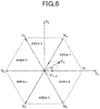
- the voltage (v ⁇ , v ⁇ ) and phase angle ( ⁇ ) are represented by a vector as shown in Fig. 6.
- Fig. 6 shows a vector diagram in which the detected voltages (V r , V s , V t ) are converted into two-phase ⁇ ⁇ coordinates system and the input voltages are observed as voltage vectors in the static coordinates system.
- V a in Fig. 6 represents a base vector and corresponds to an output command value having the phase angle ( ⁇ ) of the input voltage in the ⁇ ⁇ coordinates system.
- the base vector is rotated with a center point shown in Fig. 6 as a center in accordance with a magnitude relationship among the input voltages of the respective phases.
- the coordinates are divided with 60 degrees into six areas from ⁇ axis in the counterclockwise direction.
- Axes of V 1 through V 6 are allocated to boundary lines of the respective areas.
- the area between V 1 and V 2 is assumed as “ area 1 "
- the area between V 2 and V 3 is assumed as “ area 2 "
- the area between V 3 and V 4 is assumed as " area 3 "
- the area between V 4 and V 5 is assumed as “ area 4 "
- the area between V 5 and V 6 is assumed as " area 5"
- the area between V 6 and V 1 is assumed as " area 6 ".
- V 7 through V 9 are allocated to an origin.
- vectors of V 1 through Vg are vectors of voltages outputted from matrix converter 4.
- Vectors of V 1 through V 6 having magnitudes as the vectors (not zero) represent that the voltages not zero are outputted from matrix converter 4. That is to say, vectors of V 1 through V 6 correspond to voltage vectors not zero (hereinafter, referred to as voltage vectors).
- vectors of V 7 through V 9 represent vectors of voltage zero (zero voltage) (hereinafter, referred to as zero vectors).
- voltage vectors V 1 through V 9 are made correspond to the mutually different switching patterns of switching elements S rp , S rn , S sp , S sn , S tp , S tn and the switching patterns to operate switching elements S rp , S rn , S sp , S sn , S tp , S tn are determined dependent upon which area the input voltages belong to. It should be noted that a relationship between voltage vectors V 1 through V 9 and the switching pattern will be described later.
- space vector modulating section 12 determines which area the input voltage at a time point of detection belongs to from the phase angle ( ⁇ ) of base vector v a . In the example shown in Fig. 6 , since base vector va is within area 1, space vector modulating section 12 determines that the input voltage belongs to area 1 from the phase angle ( ⁇ ) of voltage (v ⁇ ,v ⁇ ).
- space vector modulating section 12 identifies an area 2 including phase angle of 90 degrees.
- Space vector modulating section 12 calculates an output time of the voltage vector from an area axis component of base vector (V a ) when the area is identified.
- base vector (V a ) belongs to area 1.
- Space vector modulating section 12 calculates a component (V a1 ) along V 1 axis and a component (V a2 ) along V 2 axis using V 1 axis and V 2 axis which are axes of area 1. Then, the magnitude (V a1 ) of the V 1 axis component is the output time of the switching pattern corresponding to V 1 and the magnitude (V a2 ) of the V 2 axis component is the output time of the switching pattern corresponding to V 2 .
- Each output time (T 1 , T 2 , T z ) is represented by a normalized time corresponding to the period of the carrier.
- a limitation is placed on output times (T 1 , T 2 , T z ).
- Space vector modulating section 12 calculates output times (T 1 , T 2 ) such that each of output times (T 1 , T 2 ) during which the corresponding one of the two voltage vectors is outputted is equal to or below a predetermined lowest limit value.
- the predetermined lowest limit value corresponds to a time for which output time (T z ) is secured and is set to a time shorter than the time corresponding to the half period of the carrier.
- Area 1 is a region between the phase angle of 0 degree to 60 degrees.
- the magnitude (V a1 ) of V 1 axis component is larger than magnitude (V a2 ) of the V 2 axis component.
- output time (T 1 ) of the V 1 switching pattern is longer than output time (T 2 ) of the V 2 switching pattern.
- Area 4 is a region between phase angle of 180 degrees and phase angle of 240 degrees.
- the phase angle of base vector (v a ) ranges from 210 degrees to 240 degrees
- the magnitude (V a5 ) of the V 5 axis component is larger than the magnitude (V a4 ) of the V 4 axis component.
- output time (T 2 ) of the switching pattern V 5 is longer than output time (T 1 ) of the switching pattern of V 4 .
- space vector modulating section 12 calculates the phase angle ( ⁇ ) using v ⁇ , v ⁇ corresponding to the detected voltages of the respective phases, calculates output times (T 1 , T 2 ) of the voltage vectors from the base vector V a having the calculated phase angle ( ⁇ ) as the directional component, and outputs the calculated output times (T 1 , T 2 ) to zero vector time calculating section 13.
- Zero vector time calculating section 13 subtracts a total time of output time (T 1 ) and output time (T 2 ) from a predetermined half period of the period of the carrier to calculate the time of zero vector (T z ). Since space vector modulating section 12 calculates output time (T 1 ) and output time (T 2 ) such that the above-described total time is equal to or below the predetermined lowest limit time, zero vector time calculating section 13 can calculate the time of zero vector (T z ). In this embodiment, in order to provide the alternating current for the output electric power of matrix converter 4, the time at which the non-zero voltage is outputted and the time at which the zero voltage is outputted are periodically provided.
- the output time (T z ) of the zero vector is a subtraction of the output time (T 1 ) and the output time (T 2 ) from the time corresponding to the half period of the carrier.
- Zero vector time calculating section 13 outputs the time (T z ) of the zero vector and the times (T 1 , T 2 ) of the voltage vectors to a switching signal generating section 15.
- Switching signal generating section 15 generates switching signals to drive switching elements S rp , S rn , S sp , S sn , S tp , S tn using the switching pattern stored in switching pattern table 14, the time of zero vector (T z ), and the times (T 1 , T 2 ) of the voltage vectors.
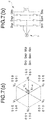
- Fig. 7(a) is an explanatory view of the vector diagram of Fig. 6 to which the switching pattern is added.
- Fig. 7(b) shows a simplified circuit diagram of alternating current power supply 1 and matrix converter 4 from among the charging system in Fig. 1 . It should be noted that “ 1 " shown in Fig. 7(a) denotes the on state and " 0 " denotes the off state.
- vectors (V 1 through V 9 ) correspond to the switching pattern of switching elements S rp , S rn , S sp , S sn , S tp , S tn .
- voltage vector (V 1 ) switching elements S rp , S tn are turned on and other switching elements S rn , S sp , S sn , S tp are turned off.
- voltage vector (V 2 ) switching elements S sp , S tn are turned on and other switching elements S rp , S rn , S sn , S tp are turned off.
- switching elements S rn , S sp are turned on and other switching elements S rp , S sp , S tp , S tn are turned off.
- switching elements S rn , S tp are turned on and other switching elements S rp , S sp , S sn , S tn are turned off.
- switching elements S sn , S tp are turned on and other switching elements S rp , S rn , S sp , S tp , S tn are turned off.
- switching elements S rp , S sn are turned on and other switching elements S rn , S sp , S tp , S tn are turned off. That is to say, in voltage vectors (V 1 through V 6 ), one of switching elements S rp , S sp , S tp , of the upper arm circuit included in one phase from among the respective phases is turned on and other switching elements S rp , S sp , S tp of the upper arm circuit included in the other phases are turned off, at least one of switching elements S rn , S sn , S tn of a lower arm circuit included in the other phases is turned on and other switching elements S rn , S sn , S tn of the lower arm circuit included in the one phase are turned off.
- the switching pattern is allocated to zero vectors (V 7 through V 9 ) shown at an origin of Fig. 7(a) .
- V 7 switching elements S rp , S rn are turned on and other switching elements S sp , S sn , S tp , S tn are turned off.
- V 8 switching elements S sp , S sn are turned on and other switching elements S rp , S rn , S tp , S tn , are turned off.
- switching elements S tp , S tn are turned on and other switching elements S rp , S rn , S sp , S sn , are turned off. That is to say, in the zero vectors (V 7 through V 9 ), switching elements S rp , S rn , S sp , S sn , S tp , S tn included in one phase from among the respective phases are turned on and switching elements S rp , S rn , S sp , S sn , S tp , S tn included in the other phases are turned off.
- one of the areas is identified according to the phase angle ( ⁇ ). Then, output voltage vectors (V 1 through V 6 ) and output time (T 1 , T 2 ) are determined. In addition, zero vector time calculating section 13 calculates zero vectors (V 7 through V 9 ) and output time (T z ) thereof.
- switching pattern table 14 stores the switching pattern which makes correspondent to the areas of Fig. 6 .
- switching signal generating section 15 calculates respective output times of vectors (V 1 through V 9 ) for the carrier period from the output times (T 1 , T 2 ) of the voltage vectors and output time (T z ) of the zero vectors and generates the switching signals.
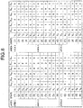
- Fig. 8 is a conceptual diagram representing the table stored in switching pattern table 14.
- areas 1 through 6 corresponds to areas 1 through 6 shown in Fig. 6 .
- V 1 through V 9 correspond to vectors (V 1 through V 9 ).
- S rp , S rn , S sp , S sn , S tp , S tn correspond to switching elements S rp , S rp , S sp , S sn , S tp , S tn .
- states (1) to (6) are derived in a time series from a summit point section of a valley of the carrier.
- matrix pattern table 14 sets the switching pattern such that two voltage vectors and one zero vector are sequentially outputted at the first (former) half period of the period of the carrier and two voltage vectors and one zero vector are sequentially outputted at the second (latter) half period of the period of the carrier.
- switching elements S rp , S rn , S sp , S sn , S tp , S tn are controlled in a sequence of voltage vector (V 1 ), voltage vector (V 2 ), zero vector (V 8 ), voltage vector (V 5 ), voltage vector (V 4 ), and zero vector (V 7 ) per period of the carrier.
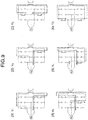
- the transition of the control of switching elements S rp , S rn , S sp , S sn , S tp , S tn in area 1 is shown in Fig. 9.
- Fig. 9 shows a circuit diagram to which the circuit diagram of alternating current power supply 1 and matrix converter 4 is simplified.
- controller 10 turns on (turns on from the off state) switching elements S rp , S rn , S sp , S sn , S tp , S tn of either one arm circuit of the upper arm circuit and the lower arm circuit and maintains the on state of switching elements S rp , S rn , S sp , S sn , S tp , S tn of the other arm circuit.
- switching elements S rp , S rp , S sp , S sn , S tp , S tn each of which is in an on state
- one of switching elements S rp , S rn , S sp , S sn , S tp , S tn is turned off but the state of the other of switching elements S rp , S rn , S sp , S sn , S tp , S tn is maintained (fixed).
- switching elements S rp , S sp , S tp , of the upper arm circuit or switching elements S rn , S sn , S tn of the lower arm circuit are not continuously switched.
- switching elements of S rp , S rn , S sp , S sn , S tp , S tn are alternately switched between the upper arm circuit and the lower arm circuit.
- the output current of matrix converter 4 indicates plus but, in states (4) through (6), the output current of matrix converter 4 indicates minus.
- the output of matrix converter 4 indicates the alternating current by controlling switching elements S rp , S rn , S sp , S sn , S tp , S tn in the switching pattern of area 1 of switching pattern table 14. It should also be noted that, for area 2, area 3, area 4, area 5, and area 6, the switching control in the pattern shown in Fig. 8 is similarly carried out to provide the alternating current for the output of matrix converter 4.
- switching pattern table 14 stores the switching pattern corresponding to phase angle (8).
- Fig. 10 is a graph for explaining a relationship between the carrier and the output times (T 1 , T 2 , T z ).
- switching signal generating section 15 sets command values corresponding to output times (T 1 , T 2 ) taking a synchronization with the period of the carrier. Since controller 10 performs the switching control through a PWM control method, lengths of the output times (T 1 , T 2 , T z ) of the voltage vectors and the zero vector indicate the command value (a voltage value).
- the command values are normalized such that a maximum amplitude of the carrier becomes the output times (T 1 , T 2 , T z ) for which two voltage vectors and one zero vector are outputted.
- the command values are set such that the voltage vectors at the more clockwise side are initially outputted in the respective areas 1 through 6 from among the voltage vectors (V 1 through V 6 ) shown in Fig. 6 . After the two voltage vectors are outputted, the command values are set such that zero vectors (V 7 through V 9 ) are outputted.
- the command values are set such that, at the second half period of the carrier, output times of the two vectors (V 1 through V 6 ) are reversed from those at the first half period of the period of the carrier and outputted and, thereafter, the zero vectors (V 7 through V 9 ) is outputted.
- switching signal generating section 15 sets the command value (T 1 ) at a level corresponding to the output time (T 1 ) with respect to the low level of the carrier and sets the command value (T 2 ) by adding the level corresponding to the output time (T 2 ) with the command value (T 1 ) as a reference, at the first half period of the carrier.
- switching signal generating section 15 sets the command value (T 2 ) at the level corresponding to output time (T 2 ) lowered from the high level of the carrier and sets the command value (T 1 ) at the level corresponding to the output time (T 1 ) with the command value (T 2 ) as the reference.
- Switching signal generating section 15 compares the carrier with the set command values to determine the output timings of the voltage vectors and the zero vector.
- the command values are set with respect to the output times (T 1 , T 2 , T z ) and are compared with the carrier so that the six states per period of the carrier are separated.
- the six states correspond to states (1) through (6) shown in Fig. 8 . That is to say, switching signal generating section 15 compares the output times (T 1 , T 2 , T z ) with the carrier to determine the output timings of the switching pattern stored in switching carrier table 14.
- Switching signal generating section 15 compares the carrier with the output times (T 1 , T 2 , T z ) to determine the output timings as shown in Fig. 10 . At this time, switching signal generating section 15 extracts the switching pattern in accordance with the phase angle ( ⁇ ) from switching pattern table 14, generates the switching signals for switching elements S rp , S rn , S sp , S sn , S tp , S tn to be driven in accordance with the extracted pattern at the output timings, and outputs the switching signals to switching elements S rp , S rn , S sp , S sn , S tp , S tn .
- the switching pattern of area 1 in Fig. 8 is used.
- the switching control outputting the voltage vector (V 1 ) is carried out.
- the switching control to output voltage vector (V 2 ) is carried out.
- the switching control to output the zero vector (V 8 ) is carried out.
- the switching control to output voltage carrier (V 5 ) is carried out.
- the switching control to output voltage vector (V 4 ) is carried out.
- the switching control to output the zero vector (V 7 ) is carried out.
- Fig. 11 shows a time characteristic of the output voltage waveform of matrix converter 4 in a case where the output time (T 1 ) is longer than the output time (T 2 ).
- Fig. 12 shows another time characteristic of the output voltage waveform of matrix converter 4 in a case where output time (T 2 ) is longer than the output time (T 1 ).
- the phase angle ( ⁇ ) falls in the range of 0 degree to 30 degrees, the output time (T 1 ) becomes longer than the output time (T 2 ).
- the voltage waveform outputted from matrix converter 4 is transited as shown in Fig. 12 .
- phase angle ( ⁇ ) is within 30 degrees through 60 degrees
- output time (T 2 ) becomes longer than output time (T 1 ) and the output voltage waveform outputted from matrix converter 4 is transited as shown in Fig. 12 .
- switching elements S rp , S rn , S sp , S sn , S tp , S tn are controlled using the output times (T 1 , T 2 ) outputting the voltage vectors and the output time (T z ) outputting the zero vector to make the output time (T z ) included in the first half period of the carrier equal to the output time (T z ) included in the second half period of the carrier.
- an inverter device (a comparative example 3) in which, in a three-phase inverter circuit formed by a bridge circuit having a plurality of switching elements, with detected voltages of intermediate voltages of the respective phases set as command values (v u *, v v *, v w *), the detected voltages are compared with a triangular wave carrier to control the switching elements is known.
- Fig. 13 shows waveforms of the carrier and command values (v u *, v v *, v w *) and the waveform of the output voltage of the inverter circuit. As shown in Fig.
- comparative example 3 uses a theoretical equation which controls the level of the output voltage when the carrier exceeds the command value and controls so as to reverse the theoretical equation with the mountain and valley of the carrier as boundaries. That is to say, in comparative example 3, the level of the output voltage is set by the comparison of the detected voltages and the carrier and the control of the output of the alternating current is carried out.
- zero voltage intervals (corresponds to ⁇ 1, ⁇ 1 in Fig. 13 ) are deviated with respect to the period of the carrier. Then, since one of the zero voltage intervals ( ⁇ 1 in Fig. 13 ) becomes relatively short, the interval of the switching operations becomes accordingly short at the first time point of the zero voltage interval and at the last time point of the zero voltage interval.
- the zero voltage interval is not prescribed as a predetermined interval with respect to the period of the carrier.
- the output time (T z ) of the zero vector with respect to the period of the carrier is secured, the interval of the switching operations at the initial time point of the zero voltage interval and the last time point of the zero voltage interval is prevented from being shortened and the commutation failure can be prevented. That is to say, as shown in Fig. 14 , the output interval of the zero vector is equally allocated to each half period of the carrier. Hence, the output time (T z ) of the zero vector is not extremely shortened so that the commutation failure can be prevented from occurring.
- Fig. 14 shows a graph for explaining the relationship between the carrier and the output times (T 1 , T 2 , T z ) and shows a time characteristic of the output voltage of matrix converter 4.
- the output time (T z ) is set to a time duration which is a subtraction result of the output times (T 1 , T 2 ) from the time corresponding to the half period of the carrier.
- the switching elements are controlled through the output time (T 1 ) during which one switching element from among the switching elements included in the upper arm circuit is turned on and one switching element from among the switching elements included in the lower arm circuit is turned on and the output time (T 2 ) during which another switching element from among the switching elements included in the upper arm circuit is turned on and another switching element from among the switching elements included in the lower arm circuit is turned on.
- T 1 the output time
- T 2 the output time
- the output time (T 1 ) is a time before the output time (T 2 ) at the first (initial) half period of the carrier and the output time (T 1 ) is a time after the output time (T 2 ) at the last half period of the carrier. This can achieve an equalization of the output time of the zero vector according to a plus side and a minus side of the output voltage of matrix converter 4.
- the output times (T 1 , T 2 , T z ) are calculated from the transformed voltages by coordinates transforming section 11, switching pattern table 14 is referred, and the switching elements (S rp , S rn , S sp , S sn , S tp , S tn ) are controlled through the switching pattern corresponding to the converted voltage phase.
- the output times (T 1 , T 2 ) of the two voltage vectors are first arranged and, subsequently, the output time (T z ) of the zero vector is arranged.
- the output times (T 1 , T 2 ) and the output time (T z ) are allocated so as to correspond to the half period of the carrier.
- These output times may correspond to be shorter than the half period of the carrier or, alternatively, to be longer than the half period of the carrier.
- a predetermined lower limit time in space vector modulating section 12 is not always a time shorter than the half period of the carrier but may be a time shorter than the time partially corresponding to the period of the carrier.
- the output times (T 1 , T 2 ) are controlled to output the two voltage vectors (V 1 through V 6 ) per half period of the carrier.
- the voltage vectors are not always the two voltage vectors (V 1 through V 6 ) but may be a single voltage vector (V 1 through V 6 ) or, alternatively, three voltage vectors (V 1 through V 6 ).
- the switching pattern shown in Fig. 8 is merely one example. Another pattern of the voltage vectors and the zero vectors may be replaced and another switching pattern to output the voltage vectors and the zero vectors may be used.
- matrix converter 4 corresponds to a conversion circuit according to the present invention
- voltage sensors 31 through 33 correspond to voltage detecting means
- controller 10 corresponds to control means
- space vector modulating section 12 and zero vector time calculating section 13 correspond to switching time calculating section
- switching signal generating section 15 corresponds to a control signal generating section
- the output times (T 1 , T 2 ) correspond to a first switching time
- the output time (T z ) correspond to a second switching time
- switching pattern table 14 corresponds to a table
- coordinates transforming section 11 corresponds to coordinates transforming means.
Applications Claiming Priority (2)
| Application Number | Priority Date | Filing Date | Title |
|---|---|---|---|
| JP2011194163A JP5377603B2 (ja) | 2011-09-06 | 2011-09-06 | 電力変換装置 |
| PCT/JP2012/072729 WO2013035782A1 (ja) | 2011-09-06 | 2012-09-06 | 電力変換装置 |
Publications (3)
| Publication Number | Publication Date |
|---|---|
| EP2755313A1 EP2755313A1 (en) | 2014-07-16 |
| EP2755313A4 EP2755313A4 (en) | 2015-10-07 |
| EP2755313B1 true EP2755313B1 (en) | 2018-11-14 |
Family
ID=47832222
Family Applications (1)
| Application Number | Title | Priority Date | Filing Date |
|---|---|---|---|
| EP12830651.1A Active EP2755313B1 (en) | 2011-09-06 | 2012-09-06 | Power conversion device |
Country Status (9)
| Country | Link |
|---|---|
| US (1) | US9197137B2 (ja) |
| EP (1) | EP2755313B1 (ja) |
| JP (1) | JP5377603B2 (ja) |
| KR (1) | KR101588147B1 (ja) |
| CN (1) | CN103765748B (ja) |
| BR (1) | BR112014000990B1 (ja) |
| MX (1) | MX2014000773A (ja) |
| RU (1) | RU2558749C1 (ja) |
| WO (1) | WO2013035782A1 (ja) |
Families Citing this family (11)
| Publication number | Priority date | Publication date | Assignee | Title |
|---|---|---|---|---|
| JP5377604B2 (ja) * | 2011-09-06 | 2013-12-25 | 日産自動車株式会社 | 電力変換装置 |
| JP5437334B2 (ja) * | 2011-09-06 | 2014-03-12 | 日産自動車株式会社 | 電力変換装置 |
| IN2013MU00006A (ja) * | 2013-06-20 | 2015-06-05 | Kraftpowercon India Private Ltd | |
| EP2993774A1 (de) * | 2014-09-05 | 2016-03-09 | AEG Power Solutions GmbH | Umrichterstufe zum Umrichten von Mehrphasenwechselstrom in Einphasenwechselstrom und umgekehrt und Verfahren zum Betreiben dieser Umrichterstufe |
| JP6477893B2 (ja) * | 2015-08-28 | 2019-03-06 | 株式会社村田製作所 | Dc−dcコンバータ |
| US20180043790A1 (en) * | 2016-08-15 | 2018-02-15 | Hamilton Sundstrand Corporation | Active rectifier topology |
| US10114782B2 (en) * | 2016-09-27 | 2018-10-30 | Nxp B.V. | USB type C dual-role-port unattached duty cycle randomization |
| US10498274B2 (en) | 2016-11-10 | 2019-12-03 | Hamilton Sundstrand Corporation | High voltage direct current system for a vehicle |
| US11043880B2 (en) | 2016-11-10 | 2021-06-22 | Hamilton Sunstrand Corporation | Electric power generating system with a synchronous generator |
| WO2018183595A1 (en) * | 2017-03-31 | 2018-10-04 | Murata Manufacturing Co., Ltd. | Apparatus and method of operating matrix converter-based rectifier when one phase is disconnected or is short-circuited |
| WO2019213673A1 (en) * | 2018-05-01 | 2019-11-07 | Murata Manufacturing Co., Ltd. | Buck matrix-type rectifier with boost switch, and operation thereof during one-phase loss |
Family Cites Families (31)
| Publication number | Priority date | Publication date | Assignee | Title |
|---|---|---|---|---|
| US5519311A (en) * | 1984-01-19 | 1996-05-21 | Don Widmayer & Associates, Inc. | Control of AC power to inductive loads |
| JP2676070B2 (ja) * | 1988-11-02 | 1997-11-12 | 日本電信電話株式会社 | 直流電源装置 |
| JPH077944A (ja) * | 1993-06-17 | 1995-01-10 | Kobe Steel Ltd | 電力変換装置の制御方法 |
| JPH08107672A (ja) * | 1994-10-04 | 1996-04-23 | Sawafuji Electric Co Ltd | 三相/二相変換回路 |
| DE19634905A1 (de) * | 1996-08-29 | 1998-03-05 | Abb Patent Gmbh | Gleichrichterschaltung |
| JP3509094B2 (ja) * | 1999-04-13 | 2004-03-22 | 株式会社安川電機 | 三相/単相pwmサイクロコンバータの制御装置 |
| US6330170B1 (en) | 1999-08-27 | 2001-12-11 | Virginia Tech Intellectual Properties, Inc. | Soft-switched quasi-single-stage (QSS) bi-directional inverter/charger |
| GB0006513D0 (en) * | 2000-03-18 | 2000-05-10 | Alstom | Improvements relating to converters |
| JP4374716B2 (ja) * | 2000-04-13 | 2009-12-02 | 富士電機システムズ株式会社 | 電力変換装置 |
| US6459606B1 (en) | 2001-09-27 | 2002-10-01 | York International Corporation | Control system and method for four-quadrant switches in three-phase PWM AC voltage regulators |
| US6462974B1 (en) * | 2001-09-27 | 2002-10-08 | York International Corporation | Space vector modulation-based control method and apparatus for three-phase pulse width modulated AC voltage regulators |
| RU2265947C2 (ru) * | 2002-07-09 | 2005-12-10 | Новоуральский государственный технологический институт | Устройство и способ управления обратимым преобразователем энергии переменного тока в энергию переменного тока |
| JP4556108B2 (ja) * | 2004-06-30 | 2010-10-06 | 富士電機ホールディングス株式会社 | 電力変換器の制御装置 |
| JP4683386B2 (ja) * | 2005-03-07 | 2011-05-18 | 国立大学法人長岡技術科学大学 | 絶縁形直接電力変換器の制御装置 |
| GB0506442D0 (en) * | 2005-03-30 | 2005-05-04 | Przybyla Jan | AC-DC converters |
| KR100949639B1 (ko) * | 2005-04-27 | 2010-03-26 | 가부시키가이샤 야스카와덴키 | 전력 변환 장치와 전력 변환 방법 |
| JP4029904B2 (ja) * | 2006-04-28 | 2008-01-09 | ダイキン工業株式会社 | マトリックスコンバータおよびマトリックスコンバータの制御方法 |
| CN102751898B (zh) * | 2006-08-10 | 2015-10-21 | 伊顿工业公司 | 环形转换器以及运行方法 |
| US8169179B2 (en) | 2006-08-22 | 2012-05-01 | Regents Of The University Of Minnesota | Open-ended control circuit for electrical apparatus |
| JP4995919B2 (ja) * | 2006-10-18 | 2012-08-08 | アーベーベー・リサーチ・リミテッド | 多数の切換え電圧レベルを切り換えるコンバータ回路 |
| WO2008108147A1 (ja) * | 2007-03-07 | 2008-09-12 | Kabushiki Kaisha Yaskawa Denki | 電力変換装置 |
| JP4957303B2 (ja) * | 2007-03-14 | 2012-06-20 | 株式会社明電舎 | 交流−交流直接変換装置の空間ベクトル変調方法 |
| RU2349019C1 (ru) * | 2008-03-11 | 2009-03-10 | Федеральное государственное образовательное учреждение высшего профессионального образования "Кубанский государственный аграрный университет" | Трехфазный преобразователь частоты с естественной коммутацией |
| JP5586872B2 (ja) * | 2009-05-07 | 2014-09-10 | 電気興業株式会社 | 三相単相直接電力変換器回路 |
| US8446743B2 (en) * | 2009-07-10 | 2013-05-21 | Regents Of The University Of Minnesota | Soft switching power electronic transformer |
| JP5282731B2 (ja) * | 2009-12-22 | 2013-09-04 | 株式会社安川電機 | 電力変換装置 |
| RU2414043C1 (ru) | 2010-03-26 | 2011-03-10 | Георгий Маркович Мустафа | Бестрансформаторный преобразователь частоты для регулируемого средневольтного электропривода |
| CN101951168B (zh) | 2010-09-16 | 2013-02-06 | 上海交通大学 | 高压转低压交流变换器 |
| CN102075109A (zh) * | 2010-12-14 | 2011-05-25 | 北京理工大学 | 高频隔离式三相周波变换器型双向变流器及其控制方法 |
| JP5377604B2 (ja) * | 2011-09-06 | 2013-12-25 | 日産自動車株式会社 | 電力変換装置 |
| JP5437334B2 (ja) * | 2011-09-06 | 2014-03-12 | 日産自動車株式会社 | 電力変換装置 |
-
2011
- 2011-09-06 JP JP2011194163A patent/JP5377603B2/ja active Active
-
2012
- 2012-09-06 KR KR1020147004992A patent/KR101588147B1/ko active IP Right Grant
- 2012-09-06 MX MX2014000773A patent/MX2014000773A/es active IP Right Grant
- 2012-09-06 RU RU2014104106/07A patent/RU2558749C1/ru active
- 2012-09-06 EP EP12830651.1A patent/EP2755313B1/en active Active
- 2012-09-06 CN CN201280035899.XA patent/CN103765748B/zh active Active
- 2012-09-06 US US14/342,842 patent/US9197137B2/en active Active
- 2012-09-06 BR BR112014000990-2A patent/BR112014000990B1/pt active IP Right Grant
- 2012-09-06 WO PCT/JP2012/072729 patent/WO2013035782A1/ja active Application Filing
Non-Patent Citations (1)
| Title |
|---|
| None * |
Also Published As
| Publication number | Publication date |
|---|---|
| US20140226382A1 (en) | 2014-08-14 |
| EP2755313A1 (en) | 2014-07-16 |
| US9197137B2 (en) | 2015-11-24 |
| KR101588147B1 (ko) | 2016-01-22 |
| WO2013035782A1 (ja) | 2013-03-14 |
| JP5377603B2 (ja) | 2013-12-25 |
| BR112014000990B1 (pt) | 2021-07-13 |
| MX2014000773A (es) | 2014-05-01 |
| KR20140042916A (ko) | 2014-04-07 |
| JP2013055866A (ja) | 2013-03-21 |
| RU2558749C1 (ru) | 2015-08-10 |
| CN103765748B (zh) | 2016-05-04 |
| BR112014000990A2 (pt) | 2017-02-21 |
| EP2755313A4 (en) | 2015-10-07 |
| CN103765748A (zh) | 2014-04-30 |
Similar Documents
| Publication | Publication Date | Title |
|---|---|---|
| EP2755313B1 (en) | Power conversion device | |
| EP2755312B1 (en) | Power conversion device | |
| EP2755311B1 (en) | Power conversion device | |
| JP6067116B2 (ja) | Dc/dcコンバータ | |
| US8233294B2 (en) | Method and system for controlling a power converter system connected to a DC-bus capacitor | |
| JP6207774B2 (ja) | Dc/dcコンバータ | |
| US9685877B2 (en) | Power conversion apparatus | |
| JP2013055868A5 (ja) | ||
| JP5045137B2 (ja) | 電力変換装置 | |
| JP2013055866A5 (ja) | ||
| JP2013055864A5 (ja) | ||
| KR20070020061A (ko) | Pwm 사이클로컨버터 및 그 제어 방법 | |
| JP6822606B2 (ja) | Dc−dcコンバータ装置 | |
| JP4274023B2 (ja) | Pwmサイクロコンバータの制御方法および制御装置 | |
| JP2021141799A (ja) | 電力変換装置 |
Legal Events
| Date | Code | Title | Description |
|---|---|---|---|
| PUAI | Public reference made under article 153(3) epc to a published international application that has entered the european phase |
Free format text: ORIGINAL CODE: 0009012 |
|
| 17P | Request for examination filed |
Effective date: 20140128 |
|
| AK | Designated contracting states |
Kind code of ref document: A1 Designated state(s): AL AT BE BG CH CY CZ DE DK EE ES FI FR GB GR HR HU IE IS IT LI LT LU LV MC MK MT NL NO PL PT RO RS SE SI SK SM TR |
|
| DAX | Request for extension of the european patent (deleted) | ||
| RA4 | Supplementary search report drawn up and despatched (corrected) |
Effective date: 20150902 |
|
| RIC1 | Information provided on ipc code assigned before grant |
Ipc: H02M 5/293 20060101AFI20150828BHEP |
|
| STAA | Information on the status of an ep patent application or granted ep patent |
Free format text: STATUS: EXAMINATION IS IN PROGRESS |
|
| 17Q | First examination report despatched |
Effective date: 20170102 |
|
| GRAP | Despatch of communication of intention to grant a patent |
Free format text: ORIGINAL CODE: EPIDOSNIGR1 |
|
| STAA | Information on the status of an ep patent application or granted ep patent |
Free format text: STATUS: GRANT OF PATENT IS INTENDED |
|
| INTG | Intention to grant announced |
Effective date: 20180730 |
|
| GRAS | Grant fee paid |
Free format text: ORIGINAL CODE: EPIDOSNIGR3 |
|
| GRAA | (expected) grant |
Free format text: ORIGINAL CODE: 0009210 |
|
| STAA | Information on the status of an ep patent application or granted ep patent |
Free format text: STATUS: THE PATENT HAS BEEN GRANTED |
|
| AK | Designated contracting states |
Kind code of ref document: B1 Designated state(s): AL AT BE BG CH CY CZ DE DK EE ES FI FR GB GR HR HU IE IS IT LI LT LU LV MC MK MT NL NO PL PT RO RS SE SI SK SM TR |
|
| REG | Reference to a national code |
Ref country code: CH Ref legal event code: EP Ref country code: AT Ref legal event code: REF Ref document number: 1066013 Country of ref document: AT Kind code of ref document: T Effective date: 20181115 |
|
| REG | Reference to a national code |
Ref country code: DE Ref legal event code: R096 Ref document number: 602012053593 Country of ref document: DE |
|
| REG | Reference to a national code |
Ref country code: IE Ref legal event code: FG4D |
|
| REG | Reference to a national code |
Ref country code: NL Ref legal event code: MP Effective date: 20181114 |
|
| REG | Reference to a national code |
Ref country code: LT Ref legal event code: MG4D |
|
| REG | Reference to a national code |
Ref country code: AT Ref legal event code: MK05 Ref document number: 1066013 Country of ref document: AT Kind code of ref document: T Effective date: 20181114 |
|
| PG25 | Lapsed in a contracting state [announced via postgrant information from national office to epo] |
Ref country code: ES Free format text: LAPSE BECAUSE OF FAILURE TO SUBMIT A TRANSLATION OF THE DESCRIPTION OR TO PAY THE FEE WITHIN THE PRESCRIBED TIME-LIMIT Effective date: 20181114 Ref country code: AT Free format text: LAPSE BECAUSE OF FAILURE TO SUBMIT A TRANSLATION OF THE DESCRIPTION OR TO PAY THE FEE WITHIN THE PRESCRIBED TIME-LIMIT Effective date: 20181114 Ref country code: IS Free format text: LAPSE BECAUSE OF FAILURE TO SUBMIT A TRANSLATION OF THE DESCRIPTION OR TO PAY THE FEE WITHIN THE PRESCRIBED TIME-LIMIT Effective date: 20190314 Ref country code: BG Free format text: LAPSE BECAUSE OF FAILURE TO SUBMIT A TRANSLATION OF THE DESCRIPTION OR TO PAY THE FEE WITHIN THE PRESCRIBED TIME-LIMIT Effective date: 20190214 Ref country code: NO Free format text: LAPSE BECAUSE OF FAILURE TO SUBMIT A TRANSLATION OF THE DESCRIPTION OR TO PAY THE FEE WITHIN THE PRESCRIBED TIME-LIMIT Effective date: 20190214 Ref country code: FI Free format text: LAPSE BECAUSE OF FAILURE TO SUBMIT A TRANSLATION OF THE DESCRIPTION OR TO PAY THE FEE WITHIN THE PRESCRIBED TIME-LIMIT Effective date: 20181114 Ref country code: LT Free format text: LAPSE BECAUSE OF FAILURE TO SUBMIT A TRANSLATION OF THE DESCRIPTION OR TO PAY THE FEE WITHIN THE PRESCRIBED TIME-LIMIT Effective date: 20181114 Ref country code: LV Free format text: LAPSE BECAUSE OF FAILURE TO SUBMIT A TRANSLATION OF THE DESCRIPTION OR TO PAY THE FEE WITHIN THE PRESCRIBED TIME-LIMIT Effective date: 20181114 Ref country code: HR Free format text: LAPSE BECAUSE OF FAILURE TO SUBMIT A TRANSLATION OF THE DESCRIPTION OR TO PAY THE FEE WITHIN THE PRESCRIBED TIME-LIMIT Effective date: 20181114 |
|
| PG25 | Lapsed in a contracting state [announced via postgrant information from national office to epo] |
Ref country code: SE Free format text: LAPSE BECAUSE OF FAILURE TO SUBMIT A TRANSLATION OF THE DESCRIPTION OR TO PAY THE FEE WITHIN THE PRESCRIBED TIME-LIMIT Effective date: 20181114 Ref country code: NL Free format text: LAPSE BECAUSE OF FAILURE TO SUBMIT A TRANSLATION OF THE DESCRIPTION OR TO PAY THE FEE WITHIN THE PRESCRIBED TIME-LIMIT Effective date: 20181114 Ref country code: RS Free format text: LAPSE BECAUSE OF FAILURE TO SUBMIT A TRANSLATION OF THE DESCRIPTION OR TO PAY THE FEE WITHIN THE PRESCRIBED TIME-LIMIT Effective date: 20181114 Ref country code: AL Free format text: LAPSE BECAUSE OF FAILURE TO SUBMIT A TRANSLATION OF THE DESCRIPTION OR TO PAY THE FEE WITHIN THE PRESCRIBED TIME-LIMIT Effective date: 20181114 Ref country code: GR Free format text: LAPSE BECAUSE OF FAILURE TO SUBMIT A TRANSLATION OF THE DESCRIPTION OR TO PAY THE FEE WITHIN THE PRESCRIBED TIME-LIMIT Effective date: 20190215 Ref country code: PT Free format text: LAPSE BECAUSE OF FAILURE TO SUBMIT A TRANSLATION OF THE DESCRIPTION OR TO PAY THE FEE WITHIN THE PRESCRIBED TIME-LIMIT Effective date: 20190314 |
|
| PG25 | Lapsed in a contracting state [announced via postgrant information from national office to epo] |
Ref country code: PL Free format text: LAPSE BECAUSE OF FAILURE TO SUBMIT A TRANSLATION OF THE DESCRIPTION OR TO PAY THE FEE WITHIN THE PRESCRIBED TIME-LIMIT Effective date: 20181114 Ref country code: DK Free format text: LAPSE BECAUSE OF FAILURE TO SUBMIT A TRANSLATION OF THE DESCRIPTION OR TO PAY THE FEE WITHIN THE PRESCRIBED TIME-LIMIT Effective date: 20181114 Ref country code: CZ Free format text: LAPSE BECAUSE OF FAILURE TO SUBMIT A TRANSLATION OF THE DESCRIPTION OR TO PAY THE FEE WITHIN THE PRESCRIBED TIME-LIMIT Effective date: 20181114 Ref country code: IT Free format text: LAPSE BECAUSE OF FAILURE TO SUBMIT A TRANSLATION OF THE DESCRIPTION OR TO PAY THE FEE WITHIN THE PRESCRIBED TIME-LIMIT Effective date: 20181114 |
|
| REG | Reference to a national code |
Ref country code: DE Ref legal event code: R097 Ref document number: 602012053593 Country of ref document: DE |
|
| PG25 | Lapsed in a contracting state [announced via postgrant information from national office to epo] |
Ref country code: SM Free format text: LAPSE BECAUSE OF FAILURE TO SUBMIT A TRANSLATION OF THE DESCRIPTION OR TO PAY THE FEE WITHIN THE PRESCRIBED TIME-LIMIT Effective date: 20181114 Ref country code: EE Free format text: LAPSE BECAUSE OF FAILURE TO SUBMIT A TRANSLATION OF THE DESCRIPTION OR TO PAY THE FEE WITHIN THE PRESCRIBED TIME-LIMIT Effective date: 20181114 Ref country code: RO Free format text: LAPSE BECAUSE OF FAILURE TO SUBMIT A TRANSLATION OF THE DESCRIPTION OR TO PAY THE FEE WITHIN THE PRESCRIBED TIME-LIMIT Effective date: 20181114 Ref country code: SK Free format text: LAPSE BECAUSE OF FAILURE TO SUBMIT A TRANSLATION OF THE DESCRIPTION OR TO PAY THE FEE WITHIN THE PRESCRIBED TIME-LIMIT Effective date: 20181114 |
|
| PLBE | No opposition filed within time limit |
Free format text: ORIGINAL CODE: 0009261 |
|
| STAA | Information on the status of an ep patent application or granted ep patent |
Free format text: STATUS: NO OPPOSITION FILED WITHIN TIME LIMIT |
|
| 26N | No opposition filed |
Effective date: 20190815 |
|
| PG25 | Lapsed in a contracting state [announced via postgrant information from national office to epo] |
Ref country code: SI Free format text: LAPSE BECAUSE OF FAILURE TO SUBMIT A TRANSLATION OF THE DESCRIPTION OR TO PAY THE FEE WITHIN THE PRESCRIBED TIME-LIMIT Effective date: 20181114 |
|
| PG25 | Lapsed in a contracting state [announced via postgrant information from national office to epo] |
Ref country code: TR Free format text: LAPSE BECAUSE OF FAILURE TO SUBMIT A TRANSLATION OF THE DESCRIPTION OR TO PAY THE FEE WITHIN THE PRESCRIBED TIME-LIMIT Effective date: 20181114 |
|
| PG25 | Lapsed in a contracting state [announced via postgrant information from national office to epo] |
Ref country code: MC Free format text: LAPSE BECAUSE OF FAILURE TO SUBMIT A TRANSLATION OF THE DESCRIPTION OR TO PAY THE FEE WITHIN THE PRESCRIBED TIME-LIMIT Effective date: 20181114 |
|
| REG | Reference to a national code |
Ref country code: CH Ref legal event code: PL |
|
| PG25 | Lapsed in a contracting state [announced via postgrant information from national office to epo] |
Ref country code: LU Free format text: LAPSE BECAUSE OF NON-PAYMENT OF DUE FEES Effective date: 20190906 Ref country code: CH Free format text: LAPSE BECAUSE OF NON-PAYMENT OF DUE FEES Effective date: 20190930 Ref country code: IE Free format text: LAPSE BECAUSE OF NON-PAYMENT OF DUE FEES Effective date: 20190906 Ref country code: LI Free format text: LAPSE BECAUSE OF NON-PAYMENT OF DUE FEES Effective date: 20190930 |
|
| REG | Reference to a national code |
Ref country code: BE Ref legal event code: MM Effective date: 20190930 |
|
| PG25 | Lapsed in a contracting state [announced via postgrant information from national office to epo] |
Ref country code: BE Free format text: LAPSE BECAUSE OF NON-PAYMENT OF DUE FEES Effective date: 20190930 |
|
| PG25 | Lapsed in a contracting state [announced via postgrant information from national office to epo] |
Ref country code: CY Free format text: LAPSE BECAUSE OF FAILURE TO SUBMIT A TRANSLATION OF THE DESCRIPTION OR TO PAY THE FEE WITHIN THE PRESCRIBED TIME-LIMIT Effective date: 20181114 |
|
| PG25 | Lapsed in a contracting state [announced via postgrant information from national office to epo] |
Ref country code: MT Free format text: LAPSE BECAUSE OF FAILURE TO SUBMIT A TRANSLATION OF THE DESCRIPTION OR TO PAY THE FEE WITHIN THE PRESCRIBED TIME-LIMIT Effective date: 20181114 Ref country code: HU Free format text: LAPSE BECAUSE OF FAILURE TO SUBMIT A TRANSLATION OF THE DESCRIPTION OR TO PAY THE FEE WITHIN THE PRESCRIBED TIME-LIMIT; INVALID AB INITIO Effective date: 20120906 |
|
| PG25 | Lapsed in a contracting state [announced via postgrant information from national office to epo] |
Ref country code: MK Free format text: LAPSE BECAUSE OF FAILURE TO SUBMIT A TRANSLATION OF THE DESCRIPTION OR TO PAY THE FEE WITHIN THE PRESCRIBED TIME-LIMIT Effective date: 20181114 |
|
| PGFP | Annual fee paid to national office [announced via postgrant information from national office to epo] |
Ref country code: GB Payment date: 20230823 Year of fee payment: 12 |
|
| PGFP | Annual fee paid to national office [announced via postgrant information from national office to epo] |
Ref country code: FR Payment date: 20230822 Year of fee payment: 12 Ref country code: DE Payment date: 20230822 Year of fee payment: 12 |