EP2747136B1 - Hochdichte organische Brückenvorrichtung und Verfahren - Google Patents
Hochdichte organische Brückenvorrichtung und Verfahren Download PDFInfo
- Publication number
- EP2747136B1 EP2747136B1 EP13196337.3A EP13196337A EP2747136B1 EP 2747136 B1 EP2747136 B1 EP 2747136B1 EP 13196337 A EP13196337 A EP 13196337A EP 2747136 B1 EP2747136 B1 EP 2747136B1
- Authority
- EP
- European Patent Office
- Prior art keywords
- bridge
- organic polymer
- organic
- interconnect structure
- high density
- Prior art date
- Legal status (The legal status is an assumption and is not a legal conclusion. Google has not performed a legal analysis and makes no representation as to the accuracy of the status listed.)
- Active
Links
Images

Classifications
-
- H—ELECTRICITY
- H10—SEMICONDUCTOR DEVICES; ELECTRIC SOLID-STATE DEVICES NOT OTHERWISE PROVIDED FOR
- H10W—GENERIC PACKAGES, INTERCONNECTIONS, CONNECTORS OR OTHER CONSTRUCTIONAL DETAILS OF DEVICES COVERED BY CLASS H10
- H10W72/00—Interconnections or connectors in packages
-
- H—ELECTRICITY
- H05—ELECTRIC TECHNIQUES NOT OTHERWISE PROVIDED FOR
- H05K—PRINTED CIRCUITS; CASINGS OR CONSTRUCTIONAL DETAILS OF ELECTRIC APPARATUS; MANUFACTURE OF ASSEMBLAGES OF ELECTRICAL COMPONENTS
- H05K1/00—Printed circuits
- H05K1/02—Details
- H05K1/14—Structural association of two or more printed circuits
- H05K1/141—One or more single auxiliary printed circuits mounted on a main printed circuit, e.g. modules, adapters
-
- H—ELECTRICITY
- H10—SEMICONDUCTOR DEVICES; ELECTRIC SOLID-STATE DEVICES NOT OTHERWISE PROVIDED FOR
- H10P—GENERIC PROCESSES OR APPARATUS FOR THE MANUFACTURE OR TREATMENT OF DEVICES COVERED BY CLASS H10
- H10P72/00—Handling or holding of wafers, substrates or devices during manufacture or treatment thereof
- H10P72/70—Handling or holding of wafers, substrates or devices during manufacture or treatment thereof for supporting or gripping
- H10P72/74—Handling or holding of wafers, substrates or devices during manufacture or treatment thereof for supporting or gripping using temporarily an auxiliary support
-
- H—ELECTRICITY
- H10—SEMICONDUCTOR DEVICES; ELECTRIC SOLID-STATE DEVICES NOT OTHERWISE PROVIDED FOR
- H10W—GENERIC PACKAGES, INTERCONNECTIONS, CONNECTORS OR OTHER CONSTRUCTIONAL DETAILS OF DEVICES COVERED BY CLASS H10
- H10W70/00—Package substrates; Interposers; Redistribution layers [RDL]
- H10W70/01—Manufacture or treatment
- H10W70/05—Manufacture or treatment of insulating or insulated package substrates, or of interposers, or of redistribution layers
- H10W70/093—Connecting or disconnecting other interconnections thereto or therefrom, e.g. connecting bond wires or bumps
-
- H—ELECTRICITY
- H10—SEMICONDUCTOR DEVICES; ELECTRIC SOLID-STATE DEVICES NOT OTHERWISE PROVIDED FOR
- H10W—GENERIC PACKAGES, INTERCONNECTIONS, CONNECTORS OR OTHER CONSTRUCTIONAL DETAILS OF DEVICES COVERED BY CLASS H10
- H10W70/00—Package substrates; Interposers; Redistribution layers [RDL]
- H10W70/01—Manufacture or treatment
- H10W70/05—Manufacture or treatment of insulating or insulated package substrates, or of interposers, or of redistribution layers
- H10W70/095—Manufacture or treatment of insulating or insulated package substrates, or of interposers, or of redistribution layers of vias therein
-
- H—ELECTRICITY
- H10—SEMICONDUCTOR DEVICES; ELECTRIC SOLID-STATE DEVICES NOT OTHERWISE PROVIDED FOR
- H10W—GENERIC PACKAGES, INTERCONNECTIONS, CONNECTORS OR OTHER CONSTRUCTIONAL DETAILS OF DEVICES COVERED BY CLASS H10
- H10W70/00—Package substrates; Interposers; Redistribution layers [RDL]
- H10W70/60—Insulating or insulated package substrates; Interposers; Redistribution layers
- H10W70/611—Insulating or insulated package substrates; Interposers; Redistribution layers for connecting multiple chips together
- H10W70/616—Insulating or insulated package substrates; Interposers; Redistribution layers for connecting multiple chips together package substrates, interposers or redistribution layers combined with bridge chips
- H10W70/618—Insulating or insulated package substrates; Interposers; Redistribution layers for connecting multiple chips together package substrates, interposers or redistribution layers combined with bridge chips the bridge chips being embedded in the package substrates, interposers or redistribution layers
-
- H—ELECTRICITY
- H10—SEMICONDUCTOR DEVICES; ELECTRIC SOLID-STATE DEVICES NOT OTHERWISE PROVIDED FOR
- H10W—GENERIC PACKAGES, INTERCONNECTIONS, CONNECTORS OR OTHER CONSTRUCTIONAL DETAILS OF DEVICES COVERED BY CLASS H10
- H10W70/00—Package substrates; Interposers; Redistribution layers [RDL]
- H10W70/60—Insulating or insulated package substrates; Interposers; Redistribution layers
- H10W70/62—Insulating or insulated package substrates; Interposers; Redistribution layers characterised by their interconnections
- H10W70/63—Vias, e.g. via plugs
- H10W70/635—Through-vias
-
- H—ELECTRICITY
- H10—SEMICONDUCTOR DEVICES; ELECTRIC SOLID-STATE DEVICES NOT OTHERWISE PROVIDED FOR
- H10W—GENERIC PACKAGES, INTERCONNECTIONS, CONNECTORS OR OTHER CONSTRUCTIONAL DETAILS OF DEVICES COVERED BY CLASS H10
- H10W70/00—Package substrates; Interposers; Redistribution layers [RDL]
- H10W70/60—Insulating or insulated package substrates; Interposers; Redistribution layers
- H10W70/62—Insulating or insulated package substrates; Interposers; Redistribution layers characterised by their interconnections
- H10W70/65—Shapes or dispositions of interconnections
-
- H—ELECTRICITY
- H10—SEMICONDUCTOR DEVICES; ELECTRIC SOLID-STATE DEVICES NOT OTHERWISE PROVIDED FOR
- H10W—GENERIC PACKAGES, INTERCONNECTIONS, CONNECTORS OR OTHER CONSTRUCTIONAL DETAILS OF DEVICES COVERED BY CLASS H10
- H10W70/00—Package substrates; Interposers; Redistribution layers [RDL]
- H10W70/60—Insulating or insulated package substrates; Interposers; Redistribution layers
- H10W70/62—Insulating or insulated package substrates; Interposers; Redistribution layers characterised by their interconnections
- H10W70/66—Conductive materials thereof
-
- H—ELECTRICITY
- H10—SEMICONDUCTOR DEVICES; ELECTRIC SOLID-STATE DEVICES NOT OTHERWISE PROVIDED FOR
- H10W—GENERIC PACKAGES, INTERCONNECTIONS, CONNECTORS OR OTHER CONSTRUCTIONAL DETAILS OF DEVICES COVERED BY CLASS H10
- H10W70/00—Package substrates; Interposers; Redistribution layers [RDL]
- H10W70/60—Insulating or insulated package substrates; Interposers; Redistribution layers
- H10W70/67—Insulating or insulated package substrates; Interposers; Redistribution layers characterised by their insulating layers or insulating parts
- H10W70/68—Shapes or dispositions thereof
- H10W70/685—Shapes or dispositions thereof comprising multiple insulating layers
-
- H—ELECTRICITY
- H10—SEMICONDUCTOR DEVICES; ELECTRIC SOLID-STATE DEVICES NOT OTHERWISE PROVIDED FOR
- H10W—GENERIC PACKAGES, INTERCONNECTIONS, CONNECTORS OR OTHER CONSTRUCTIONAL DETAILS OF DEVICES COVERED BY CLASS H10
- H10W70/00—Package substrates; Interposers; Redistribution layers [RDL]
- H10W70/60—Insulating or insulated package substrates; Interposers; Redistribution layers
- H10W70/67—Insulating or insulated package substrates; Interposers; Redistribution layers characterised by their insulating layers or insulating parts
- H10W70/69—Insulating materials thereof
- H10W70/695—Organic materials
-
- H—ELECTRICITY
- H10—SEMICONDUCTOR DEVICES; ELECTRIC SOLID-STATE DEVICES NOT OTHERWISE PROVIDED FOR
- H10W—GENERIC PACKAGES, INTERCONNECTIONS, CONNECTORS OR OTHER CONSTRUCTIONAL DETAILS OF DEVICES COVERED BY CLASS H10
- H10W90/00—Package configurations
-
- H—ELECTRICITY
- H10—SEMICONDUCTOR DEVICES; ELECTRIC SOLID-STATE DEVICES NOT OTHERWISE PROVIDED FOR
- H10W—GENERIC PACKAGES, INTERCONNECTIONS, CONNECTORS OR OTHER CONSTRUCTIONAL DETAILS OF DEVICES COVERED BY CLASS H10
- H10W90/00—Package configurations
- H10W90/401—Package configurations characterised by multiple insulating or insulated package substrates, interposers or RDLs
-
- H—ELECTRICITY
- H10—SEMICONDUCTOR DEVICES; ELECTRIC SOLID-STATE DEVICES NOT OTHERWISE PROVIDED FOR
- H10W—GENERIC PACKAGES, INTERCONNECTIONS, CONNECTORS OR OTHER CONSTRUCTIONAL DETAILS OF DEVICES COVERED BY CLASS H10
- H10W90/00—Package configurations
- H10W90/701—Package configurations characterised by the relative positions of pads or connectors relative to package parts
-
- H—ELECTRICITY
- H05—ELECTRIC TECHNIQUES NOT OTHERWISE PROVIDED FOR
- H05K—PRINTED CIRCUITS; CASINGS OR CONSTRUCTIONAL DETAILS OF ELECTRIC APPARATUS; MANUFACTURE OF ASSEMBLAGES OF ELECTRICAL COMPONENTS
- H05K1/00—Printed circuits
- H05K1/02—Details
- H05K1/03—Use of materials for the substrate
- H05K1/0313—Organic insulating material
-
- H—ELECTRICITY
- H05—ELECTRIC TECHNIQUES NOT OTHERWISE PROVIDED FOR
- H05K—PRINTED CIRCUITS; CASINGS OR CONSTRUCTIONAL DETAILS OF ELECTRIC APPARATUS; MANUFACTURE OF ASSEMBLAGES OF ELECTRICAL COMPONENTS
- H05K1/00—Printed circuits
- H05K1/02—Details
- H05K1/14—Structural association of two or more printed circuits
- H05K1/142—Arrangements of planar printed circuit boards in the same plane, e.g. auxiliary printed circuit insert mounted in a main printed circuit
-
- H—ELECTRICITY
- H05—ELECTRIC TECHNIQUES NOT OTHERWISE PROVIDED FOR
- H05K—PRINTED CIRCUITS; CASINGS OR CONSTRUCTIONAL DETAILS OF ELECTRIC APPARATUS; MANUFACTURE OF ASSEMBLAGES OF ELECTRICAL COMPONENTS
- H05K1/00—Printed circuits
- H05K1/18—Printed circuits structurally associated with non-printed electric components
- H05K1/181—Printed circuits structurally associated with non-printed electric components associated with surface mounted components
-
- H—ELECTRICITY
- H05—ELECTRIC TECHNIQUES NOT OTHERWISE PROVIDED FOR
- H05K—PRINTED CIRCUITS; CASINGS OR CONSTRUCTIONAL DETAILS OF ELECTRIC APPARATUS; MANUFACTURE OF ASSEMBLAGES OF ELECTRICAL COMPONENTS
- H05K2201/00—Indexing scheme relating to printed circuits covered by H05K1/00
- H05K2201/04—Assemblies of printed circuits
- H05K2201/048—Second PCB mounted on first PCB by inserting in window or holes of the first PCB
-
- H—ELECTRICITY
- H05—ELECTRIC TECHNIQUES NOT OTHERWISE PROVIDED FOR
- H05K—PRINTED CIRCUITS; CASINGS OR CONSTRUCTIONAL DETAILS OF ELECTRIC APPARATUS; MANUFACTURE OF ASSEMBLAGES OF ELECTRICAL COMPONENTS
- H05K2201/00—Indexing scheme relating to printed circuits covered by H05K1/00
- H05K2201/04—Assemblies of printed circuits
- H05K2201/049—PCB for one component, e.g. for mounting onto mother PCB
-
- H—ELECTRICITY
- H05—ELECTRIC TECHNIQUES NOT OTHERWISE PROVIDED FOR
- H05K—PRINTED CIRCUITS; CASINGS OR CONSTRUCTIONAL DETAILS OF ELECTRIC APPARATUS; MANUFACTURE OF ASSEMBLAGES OF ELECTRICAL COMPONENTS
- H05K2201/00—Indexing scheme relating to printed circuits covered by H05K1/00
- H05K2201/10—Details of components or other objects attached to or integrated in a printed circuit board
- H05K2201/10431—Details of mounted components
- H05K2201/10507—Involving several components
- H05K2201/10522—Adjacent components
-
- H—ELECTRICITY
- H05—ELECTRIC TECHNIQUES NOT OTHERWISE PROVIDED FOR
- H05K—PRINTED CIRCUITS; CASINGS OR CONSTRUCTIONAL DETAILS OF ELECTRIC APPARATUS; MANUFACTURE OF ASSEMBLAGES OF ELECTRICAL COMPONENTS
- H05K2201/00—Indexing scheme relating to printed circuits covered by H05K1/00
- H05K2201/10—Details of components or other objects attached to or integrated in a printed circuit board
- H05K2201/10613—Details of electrical connections of non-printed components, e.g. special leads
- H05K2201/10621—Components characterised by their electrical contacts
- H05K2201/10674—Flip chip
-
- H—ELECTRICITY
- H05—ELECTRIC TECHNIQUES NOT OTHERWISE PROVIDED FOR
- H05K—PRINTED CIRCUITS; CASINGS OR CONSTRUCTIONAL DETAILS OF ELECTRIC APPARATUS; MANUFACTURE OF ASSEMBLAGES OF ELECTRICAL COMPONENTS
- H05K2203/00—Indexing scheme relating to apparatus or processes for manufacturing printed circuits covered by H05K3/00
- H05K2203/01—Tools for processing; Objects used during processing
- H05K2203/0147—Carriers and holders
- H05K2203/016—Temporary inorganic, non-metallic carrier, e.g. for processing or transferring
-
- H—ELECTRICITY
- H05—ELECTRIC TECHNIQUES NOT OTHERWISE PROVIDED FOR
- H05K—PRINTED CIRCUITS; CASINGS OR CONSTRUCTIONAL DETAILS OF ELECTRIC APPARATUS; MANUFACTURE OF ASSEMBLAGES OF ELECTRICAL COMPONENTS
- H05K3/00—Apparatus or processes for manufacturing printed circuits
- H05K3/30—Assembling printed circuits with electric components, e.g. with resistors
- H05K3/32—Assembling printed circuits with electric components, e.g. with resistors electrically connecting electric components or wires to printed circuits
- H05K3/34—Assembling printed circuits with electric components, e.g. with resistors electrically connecting electric components or wires to printed circuits by soldering
- H05K3/341—Surface mounted components
- H05K3/3431—Leadless components
- H05K3/3436—Leadless components having an array of bottom contacts, e.g. pad grid array or ball grid array components
-
- H—ELECTRICITY
- H05—ELECTRIC TECHNIQUES NOT OTHERWISE PROVIDED FOR
- H05K—PRINTED CIRCUITS; CASINGS OR CONSTRUCTIONAL DETAILS OF ELECTRIC APPARATUS; MANUFACTURE OF ASSEMBLAGES OF ELECTRICAL COMPONENTS
- H05K3/00—Apparatus or processes for manufacturing printed circuits
- H05K3/46—Manufacturing multilayer circuits
- H05K3/4644—Manufacturing multilayer circuits by building the multilayer layer by layer, i.e. build-up multilayer circuits
- H05K3/467—Adding a circuit layer by thin film methods
-
- H—ELECTRICITY
- H10—SEMICONDUCTOR DEVICES; ELECTRIC SOLID-STATE DEVICES NOT OTHERWISE PROVIDED FOR
- H10P—GENERIC PROCESSES OR APPARATUS FOR THE MANUFACTURE OR TREATMENT OF DEVICES COVERED BY CLASS H10
- H10P72/00—Handling or holding of wafers, substrates or devices during manufacture or treatment thereof
- H10P72/70—Handling or holding of wafers, substrates or devices during manufacture or treatment thereof for supporting or gripping
- H10P72/74—Handling or holding of wafers, substrates or devices during manufacture or treatment thereof for supporting or gripping using temporarily an auxiliary support
- H10P72/7424—Handling or holding of wafers, substrates or devices during manufacture or treatment thereof for supporting or gripping using temporarily an auxiliary support used as a support during the manufacture of self-supporting substrates
-
- H—ELECTRICITY
- H10—SEMICONDUCTOR DEVICES; ELECTRIC SOLID-STATE DEVICES NOT OTHERWISE PROVIDED FOR
- H10W—GENERIC PACKAGES, INTERCONNECTIONS, CONNECTORS OR OTHER CONSTRUCTIONAL DETAILS OF DEVICES COVERED BY CLASS H10
- H10W70/00—Package substrates; Interposers; Redistribution layers [RDL]
- H10W70/60—Insulating or insulated package substrates; Interposers; Redistribution layers
- H10W70/62—Insulating or insulated package substrates; Interposers; Redistribution layers characterised by their interconnections
- H10W70/63—Vias, e.g. via plugs
-
- H—ELECTRICITY
- H10—SEMICONDUCTOR DEVICES; ELECTRIC SOLID-STATE DEVICES NOT OTHERWISE PROVIDED FOR
- H10W—GENERIC PACKAGES, INTERCONNECTIONS, CONNECTORS OR OTHER CONSTRUCTIONAL DETAILS OF DEVICES COVERED BY CLASS H10
- H10W72/00—Interconnections or connectors in packages
- H10W72/071—Connecting or disconnecting
- H10W72/072—Connecting or disconnecting of bump connectors
- H10W72/07231—Techniques
- H10W72/07232—Compression bonding, e.g. thermocompression bonding
-
- H—ELECTRICITY
- H10—SEMICONDUCTOR DEVICES; ELECTRIC SOLID-STATE DEVICES NOT OTHERWISE PROVIDED FOR
- H10W—GENERIC PACKAGES, INTERCONNECTIONS, CONNECTORS OR OTHER CONSTRUCTIONAL DETAILS OF DEVICES COVERED BY CLASS H10
- H10W72/00—Interconnections or connectors in packages
- H10W72/071—Connecting or disconnecting
- H10W72/072—Connecting or disconnecting of bump connectors
- H10W72/07251—Connecting or disconnecting of bump connectors characterised by changes in properties of the bump connectors during connecting
- H10W72/07252—Connecting or disconnecting of bump connectors characterised by changes in properties of the bump connectors during connecting changes in structures or sizes
-
- H—ELECTRICITY
- H10—SEMICONDUCTOR DEVICES; ELECTRIC SOLID-STATE DEVICES NOT OTHERWISE PROVIDED FOR
- H10W—GENERIC PACKAGES, INTERCONNECTIONS, CONNECTORS OR OTHER CONSTRUCTIONAL DETAILS OF DEVICES COVERED BY CLASS H10
- H10W72/00—Interconnections or connectors in packages
- H10W72/20—Bump connectors, e.g. solder bumps or copper pillars; Dummy bumps; Thermal bumps
- H10W72/221—Structures or relative sizes
- H10W72/227—Multiple bumps having different sizes
-
- H—ELECTRICITY
- H10—SEMICONDUCTOR DEVICES; ELECTRIC SOLID-STATE DEVICES NOT OTHERWISE PROVIDED FOR
- H10W—GENERIC PACKAGES, INTERCONNECTIONS, CONNECTORS OR OTHER CONSTRUCTIONAL DETAILS OF DEVICES COVERED BY CLASS H10
- H10W72/00—Interconnections or connectors in packages
- H10W72/20—Bump connectors, e.g. solder bumps or copper pillars; Dummy bumps; Thermal bumps
- H10W72/241—Dispositions, e.g. layouts
-
- H—ELECTRICITY
- H10—SEMICONDUCTOR DEVICES; ELECTRIC SOLID-STATE DEVICES NOT OTHERWISE PROVIDED FOR
- H10W—GENERIC PACKAGES, INTERCONNECTIONS, CONNECTORS OR OTHER CONSTRUCTIONAL DETAILS OF DEVICES COVERED BY CLASS H10
- H10W90/00—Package configurations
- H10W90/701—Package configurations characterised by the relative positions of pads or connectors relative to package parts
- H10W90/721—Package configurations characterised by the relative positions of pads or connectors relative to package parts of bump connectors
- H10W90/724—Package configurations characterised by the relative positions of pads or connectors relative to package parts of bump connectors between a chip and a stacked insulating package substrate, interposer or RDL
Definitions
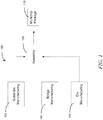
- Die manufacturing process 106 is illustrated in dashed form to indicate that the die can be assembled on the substrate and bridge in the same process 108 or in a separate process at a later time. Die manufacturing process 106 can be any process sufficient to produce desired dies that will be incorporated into the final product. No further description of die manufacturing 106 will be given as it is not important to the disclosure herein.
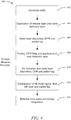
- Substrate 302 may comprise connection points 306 to connect a die, such as die 318 and 319 to substrate 302. Connection points 306 and associated conductive paths (not shown) may adhere to design rules appropriate for substrate 302. In one embodiment, the design rules of substrate 302 allow larger geometries (for e.g. connection points 306) than the design rules of embedded organic bridge 304. In one example, substrate 302 can be produced using design rules of about a 40 ⁇ m wire width and about a 40 ⁇ m wire spacing. Similarly, build-up layers, if any, can be thicker than those in organic bridge 304.
- organic bridges 304 are only a few layers thick, perhaps only the routing layer 314 , pad layer 316, ground and reference layers for the signal layers, plus interleaved dielectric layers 312. In such a situation, this two layer organic bridge 304 will be about 15 ⁇ m thick. However, if desired, the process illustrated in 408 and/or 410 can be repeated as appropriate to achieve an organic bridge 304 of perhaps three or four layers having a thickness of about 20 ⁇ m to about 30 ⁇ m.
Landscapes
- Engineering & Computer Science (AREA)
- Microelectronics & Electronic Packaging (AREA)
- Internal Circuitry In Semiconductor Integrated Circuit Devices (AREA)
- Physics & Mathematics (AREA)
- Geometry (AREA)
- Production Of Multi-Layered Print Wiring Board (AREA)
- Wire Bonding (AREA)
- Combinations Of Printed Boards (AREA)
Claims (12)
- Mikroelektronisches Bauelement (200), umfassend:ein organisches Polymersubstrat (212);eine organische Polymerbrücke (214), eingebettet in dem Substrat, die organische Polymerbrücke umfassend:eine Metallleitschicht (314);eine Metallzwischenschicht (316);verschachtelte organische dielektrische Polymerschichten (312);eine erste Verschaltungsstruktur hoher Dichte (204) an einem ersten Ort der organischen Polymerbrücke, die erste Verschaltungsstruktur angepasst zum Verbinden mit einem ersten Plättchen;eine zweite Verschaltungsstruktur hoher Dichte (204) an einem zweiten Ort der organischen Polymerbrücke, die zweite Verschaltungsstruktur angepasst zum Verbinden mit einem zweiten Plättchen;einen elektrisch leitenden Weg in der organischen Polymerbrücke, der die erste Verschaltungsstruktur hoher Dichte mit der zweiten Verschaltungsstruktur hoher Dichte verbindet, undwobei das organische Polymersubstrat eine Aussparung enthält und die organische Polymerbrücke in der Aussparung eingebettet ist und unter Verwendung eines organischen Polymers daran gebondet ist.
- Mikroelektronisches Bauelement nach Anspruch 1, wobei Drähte des organischen Polymersubstrats eine erste Drahtbreite und eine erste Drahtbeabstandung aufweisen und wobei Drähte der organischen Polymerbrücke eine zweite Drahtbreite und eine zweite Drahtbeabstandung aufweisen.
- Mikroelektronisches Bauelement nach Anspruch 1 oder 2, wobei die erste Drahtbreite größer ist als die zweite Drahtbreite und die erste Drahtbeabstandung größer ist als die zweite Drahtbeabstandung.
- Mikroelektronisches Bauelement nach Anspruch 1, 2 oder 3, wobei die organische Polymerbrücke eine gesamte Dicke von weniger als 20 µm aufweist.
- Organische Polymerbrücke, angepasst zum Verschalten einer Vielzahl von Plättchen, die organische Polymerbrücke umfassend:eine Metallleitschicht;eine Metallzwischenschicht;verschachtelte organische dielektrische Polymerschichten; undeine erste Verschaltungsstruktur hoher Dichte an einem ersten Ort der organischen Polymerbrücke, die erste Verschaltungsstruktur hoher Dichte angepasst zum Verbinden mit einem ersten Plättchen;eine zweite Verschaltungsstruktur hoher Dichte an einem zweiten Ort der organischen Polymerbrücke, die zweite Verschaltungsstruktur angepasst zum Verbinden mit einem zweiten Plättchen;einen elektrisch leitenden Weg in der organischen Polymerbrücke, der die erste Verschaltungsstruktur hoher Dichte mit der zweiten Verschaltungsstruktur hoher Dichte verbindet; undwobei die organische Polymerbrücke angepasst ist, in eine Aussparung in einem organischen Polymersubstrat eingebettet und unter Verwendung eines organischen Polymers daran gebondet zu werden.
- Organische Brücke nach Anspruch 5, wobei alle Schichten eine kombinierte Dicke von weniger als 30 µm aufweisen.
- Organische Brücke nach Anspruch 5, wobei alle Schichten eine kombinierte Dicke von etwa 15 µm aufweisen.
- Organische Brücke nach Anspruch 5, 6 oder 7, ferner umfassend eine zusätzliche Metallschicht und eine zusätzliche verschachtelte organische dielektrische Polymerschicht.
- Verfahren, umfassend:
Bereitstellen einer organischen Polymerbrücke, umfassend:eine Metallleitschicht;eine Metallzwischenschicht;verschachtelte organische dielektrische Polymerschichten;eine erste Verschaltungsstruktur hoher Dichte an einem ersten Ort der organischen Polymerbrücke, die erste Verschaltungsstruktur angepasst zum Verbinden mit einem ersten Plättchen;eine zweite Verschaltungsstruktur hoher Dichte an einem zweiten Ort der organischen Polymerbrücke, die zweite Verschaltungsstruktur angepasst zum Verbinden mit einem zweiten Plättchen;einen elektrisch leitenden Weg, der die erste Verschaltungsstruktur hoher Dichte mit der zweiten Verschaltungsstruktur hoher Dichte verbindet;Bereitstellen eines organischen Bauelementpolymersubstrats mit einer darin gebildeten Aussparung; undEinbetten der organischen Polymerbrücke in die Aussparung des organischen Bauelementpolymersubstrats unter Verwendung eines organischen Polymers. - Verfahren nach Anspruch 9, wobei alle Schichten der organischen Brücke eine Dicke von weniger als 15 µm aufweisen.
- Verfahren nach Anspruch 9, wobei alle Schichten der organischen Brücke eine Dicke von weniger als 20 µm aufweisen.
- Verfahren nach Anspruch 9, 10 oder 11, wobei die Metallzwischenschicht eine Vielzahl von Verschaltungen umfasst und wobei das Verfahren ferner umfasst, ein erstes Plättchen an eine der Vielzahl von Verschaltungen zu bonden und ein zweites Plättchen an eine andere eine der Vielzahl von Verschaltungen zu bonden, wobei das Bonden des ersten Plättchens und des zweiten Plättchens unter Verwendung von Thermokompressionsbonden durchgeführt wird.
Priority Applications (2)
| Application Number | Priority Date | Filing Date | Title |
|---|---|---|---|
| EP24186432.1A EP4440253A3 (de) | 2012-12-20 | 2013-12-09 | Hochdichte organische brückenvorrichtung und verfahren |
| EP17188479.4A EP3273476A1 (de) | 2012-12-20 | 2013-12-09 | Hohe dichte organische brückenvorrichtung und verfahren |
Applications Claiming Priority (2)
| Application Number | Priority Date | Filing Date | Title |
|---|---|---|---|
| US13/722,203 US9236366B2 (en) | 2012-12-20 | 2012-12-20 | High density organic bridge device and method |
| PCT/US2013/044440 WO2014098966A1 (en) | 2012-12-20 | 2013-06-06 | High density organic bridge device and method |
Related Child Applications (3)
| Application Number | Title | Priority Date | Filing Date |
|---|---|---|---|
| EP17188479.4A Division EP3273476A1 (de) | 2012-12-20 | 2013-12-09 | Hohe dichte organische brückenvorrichtung und verfahren |
| EP17188479.4A Division-Into EP3273476A1 (de) | 2012-12-20 | 2013-12-09 | Hohe dichte organische brückenvorrichtung und verfahren |
| EP24186432.1A Division EP4440253A3 (de) | 2012-12-20 | 2013-12-09 | Hochdichte organische brückenvorrichtung und verfahren |
Publications (2)
| Publication Number | Publication Date |
|---|---|
| EP2747136A1 EP2747136A1 (de) | 2014-06-25 |
| EP2747136B1 true EP2747136B1 (de) | 2019-11-20 |
Family
ID=50973358
Family Applications (3)
| Application Number | Title | Priority Date | Filing Date |
|---|---|---|---|
| EP13196337.3A Active EP2747136B1 (de) | 2012-12-20 | 2013-12-09 | Hochdichte organische Brückenvorrichtung und Verfahren |
| EP24186432.1A Pending EP4440253A3 (de) | 2012-12-20 | 2013-12-09 | Hochdichte organische brückenvorrichtung und verfahren |
| EP17188479.4A Ceased EP3273476A1 (de) | 2012-12-20 | 2013-12-09 | Hohe dichte organische brückenvorrichtung und verfahren |
Family Applications After (2)
| Application Number | Title | Priority Date | Filing Date |
|---|---|---|---|
| EP24186432.1A Pending EP4440253A3 (de) | 2012-12-20 | 2013-12-09 | Hochdichte organische brückenvorrichtung und verfahren |
| EP17188479.4A Ceased EP3273476A1 (de) | 2012-12-20 | 2013-12-09 | Hohe dichte organische brückenvorrichtung und verfahren |
Country Status (9)
| Country | Link |
|---|---|
| US (6) | US9236366B2 (de) |
| EP (3) | EP2747136B1 (de) |
| JP (3) | JP2014140022A (de) |
| KR (2) | KR101593277B1 (de) |
| CN (1) | CN104037161B (de) |
| BR (1) | BR102013032406B1 (de) |
| SG (1) | SG2013093521A (de) |
| TW (1) | TWI556401B (de) |
| WO (1) | WO2014098966A1 (de) |
Families Citing this family (58)
| Publication number | Priority date | Publication date | Assignee | Title |
|---|---|---|---|---|
| US8227904B2 (en) * | 2009-06-24 | 2012-07-24 | Intel Corporation | Multi-chip package and method of providing die-to-die interconnects in same |
| US9136236B2 (en) | 2012-09-28 | 2015-09-15 | Intel Corporation | Localized high density substrate routing |
| US9190380B2 (en) | 2012-12-06 | 2015-11-17 | Intel Corporation | High density substrate routing in BBUL package |
| US9236366B2 (en) | 2012-12-20 | 2016-01-12 | Intel Corporation | High density organic bridge device and method |
| US8901748B2 (en) * | 2013-03-14 | 2014-12-02 | Intel Corporation | Direct external interconnect for embedded interconnect bridge package |
| US9147663B2 (en) * | 2013-05-28 | 2015-09-29 | Intel Corporation | Bridge interconnection with layered interconnect structures |
| JP2014236188A (ja) * | 2013-06-05 | 2014-12-15 | イビデン株式会社 | 配線板及びその製造方法 |
| US9041205B2 (en) * | 2013-06-28 | 2015-05-26 | Intel Corporation | Reliable microstrip routing for electronics components |
| US9642259B2 (en) * | 2013-10-30 | 2017-05-02 | Qualcomm Incorporated | Embedded bridge structure in a substrate |
| US20150364422A1 (en) * | 2014-06-13 | 2015-12-17 | Apple Inc. | Fan out wafer level package using silicon bridge |
| JP2016021496A (ja) * | 2014-07-15 | 2016-02-04 | イビデン株式会社 | 配線基板及びその製造方法 |
| KR102262178B1 (ko) | 2014-09-19 | 2021-06-07 | 인텔 코포레이션 | 내장형 브릿지 상호접속부를 가진 반도체 패키지 |
| US9583426B2 (en) | 2014-11-05 | 2017-02-28 | Invensas Corporation | Multi-layer substrates suitable for interconnection between circuit modules |
| US9595496B2 (en) * | 2014-11-07 | 2017-03-14 | Qualcomm Incorporated | Integrated device package comprising silicon bridge in an encapsulation layer |
| US9379090B1 (en) * | 2015-02-13 | 2016-06-28 | Qualcomm Incorporated | System, apparatus, and method for split die interconnection |
| US9443824B1 (en) | 2015-03-30 | 2016-09-13 | Qualcomm Incorporated | Cavity bridge connection for die split architecture |
| US10283492B2 (en) | 2015-06-23 | 2019-05-07 | Invensas Corporation | Laminated interposers and packages with embedded trace interconnects |
| US10477684B2 (en) * | 2015-09-25 | 2019-11-12 | Intel Corporation | Apparatus, system, and method including a bridge device for interfacing a package device with a substrate |
| US10177083B2 (en) | 2015-10-29 | 2019-01-08 | Intel Corporation | Alternative surfaces for conductive pad layers of silicon bridges for semiconductor packages |
| CN108292654A (zh) | 2015-12-11 | 2018-07-17 | 英特尔公司 | 具有利用嵌入微电子衬底中的微电子桥连接的多个微电子器件的微电子结构 |
| US9852994B2 (en) | 2015-12-14 | 2017-12-26 | Invensas Corporation | Embedded vialess bridges |
| WO2017111790A1 (en) * | 2015-12-23 | 2017-06-29 | Manusharow Mathew J | Improving size and efficiency of dies |
| TWI652778B (zh) * | 2016-01-27 | 2019-03-01 | Amkor Technology, Inc. | 半導體封裝以及其製造方法 |
| KR101966328B1 (ko) * | 2016-03-29 | 2019-04-05 | 삼성전기주식회사 | 인쇄회로기판 및 그 제조방법 |
| US11114353B2 (en) | 2016-03-30 | 2021-09-07 | Intel Corporation | Hybrid microelectronic substrates |
| US20170287838A1 (en) | 2016-04-02 | 2017-10-05 | Intel Corporation | Electrical interconnect bridge |
| WO2018004620A1 (en) * | 2016-06-30 | 2018-01-04 | Qian Zhiguo | Bridge die design for high bandwidth memory interface |
| WO2018004692A1 (en) | 2016-07-01 | 2018-01-04 | Pietambaram Srinivas V | Molded embedded bridge for enhanced emib applications |
| KR102632563B1 (ko) | 2016-08-05 | 2024-02-02 | 삼성전자주식회사 | 반도체 패키지 |
| KR102595896B1 (ko) * | 2016-08-08 | 2023-10-30 | 삼성전자 주식회사 | 인쇄회로기판 및 이를 가지는 반도체 패키지 |
| EP3288076B1 (de) * | 2016-08-25 | 2021-06-23 | IMEC vzw | Halbleiterchipgehäuse und verfahren zur herstellung des gehäuses |
| WO2018098650A1 (zh) * | 2016-11-30 | 2018-06-07 | 深圳修远电子科技有限公司 | 集成电路封装结构及方法 |
| US11004824B2 (en) | 2016-12-22 | 2021-05-11 | Intel Corporation | Scalable embedded silicon bridge via pillars in lithographically defined vias, and methods of making same |
| US10943869B2 (en) | 2017-06-09 | 2021-03-09 | Apple Inc. | High density interconnection using fanout interposer chiplet |
| US10622311B2 (en) * | 2017-08-10 | 2020-04-14 | International Business Machines Corporation | High-density interconnecting adhesive tape |
| CN111052369A (zh) * | 2017-09-29 | 2020-04-21 | 英特尔公司 | 使用嵌入式桥管芯的水平间距转换 |
| US10483156B2 (en) * | 2017-11-29 | 2019-11-19 | International Business Machines Corporation | Non-embedded silicon bridge chip for multi-chip module |
| US10784202B2 (en) | 2017-12-01 | 2020-09-22 | International Business Machines Corporation | High-density chip-to-chip interconnection with silicon bridge |
| JP6912423B2 (ja) * | 2018-01-04 | 2021-08-04 | 株式会社東芝 | 電子装置 |
| US10475767B2 (en) | 2018-01-04 | 2019-11-12 | Kabushiki Kaisha Toshiba | Electronic device |
| US10580738B2 (en) * | 2018-03-20 | 2020-03-03 | International Business Machines Corporation | Direct bonded heterogeneous integration packaging structures |
| TWI662676B (zh) * | 2018-08-31 | 2019-06-11 | 欣興電子股份有限公司 | 具有內埋基板的線路載板及其製作方法與晶片封裝結構 |
| US11018124B2 (en) | 2018-08-31 | 2021-05-25 | Intel Corporation | Embedded memory device and method for embedding memory device in a substrate |
| TWI862101B (zh) * | 2018-12-07 | 2024-11-11 | 新加坡商安靠科技新加坡控股私人有限公司 | 半導體封裝和其製造方法 |
| CN111372369B (zh) | 2018-12-25 | 2023-07-07 | 奥特斯科技(重庆)有限公司 | 具有部件屏蔽的部件承载件及其制造方法 |
| US11756889B2 (en) * | 2019-08-07 | 2023-09-12 | Intel Corporation | Ultrathin bridge and multi-die ultrafine pitch patch architecture and method of making |
| US11569172B2 (en) | 2019-08-08 | 2023-01-31 | Taiwan Semiconductor Manufacturing Co., Ltd. | Semiconductor devices and methods of manufacture |
| US10957650B2 (en) | 2019-08-21 | 2021-03-23 | International Business Machines Corporation | Bridge support structure |
| US11527462B2 (en) | 2019-12-13 | 2022-12-13 | International Business Machines Corporation | Circuit substrate with mixed pitch wiring |
| CN111769101B (zh) * | 2020-07-09 | 2022-05-03 | 中国科学院微电子研究所 | 一种基于多转接板的封装结构及封装方法 |
| US11532582B2 (en) * | 2020-08-25 | 2022-12-20 | Taiwan Semiconductor Manufacturing Co., Ltd. | Semiconductor device package and method of manufacture |
| US20230317619A1 (en) * | 2022-04-01 | 2023-10-05 | Intel Corporation | Microelectronic structure including die bonding film between embedded die and surface of substrate cavity, and method of making same |
| US12463178B2 (en) * | 2022-07-03 | 2025-11-04 | Taiwan Semiconductor Manufacturing Company, Ltd. | Semiconductor die assembly having a polygonal linking die |
| CN119768918A (zh) * | 2022-09-09 | 2025-04-04 | 超极存储器股份有限公司 | Ic桥、ic模块及ic模块的制造方法 |
| CN116053251A (zh) * | 2022-12-13 | 2023-05-02 | 海光信息技术股份有限公司 | 封装结构、芯片、电子设备及芯片封装方法 |
| CN120958975A (zh) | 2023-03-30 | 2025-11-14 | 索尼半导体解决方案公司 | 基板装置、电子设备、电子装置、电子设备的制造方法和电子装置的制造方法 |
| CN116092948B (zh) * | 2023-04-10 | 2025-02-28 | 北京华封集芯电子有限公司 | 一种制作芯片的方法及芯片 |
| WO2024212974A1 (zh) * | 2023-04-10 | 2024-10-17 | 北京华封集芯电子有限公司 | 一种制作中介层、芯片的方法、中介层、芯片及芯片封装 |
Family Cites Families (60)
| Publication number | Priority date | Publication date | Assignee | Title |
|---|---|---|---|---|
| US3436604A (en) * | 1966-04-25 | 1969-04-01 | Texas Instruments Inc | Complex integrated circuit array and method for fabricating same |
| US3684818A (en) * | 1970-10-20 | 1972-08-15 | Sprague Electric Co | Multi-layer beam-lead wiring for semiconductor packages |
| JPS4989157A (de) * | 1972-12-29 | 1974-08-26 | ||
| US4054938A (en) * | 1974-05-13 | 1977-10-18 | American Microsystems, Inc. | Combined semiconductor device and printed circuit board assembly |
| US4055725A (en) * | 1974-05-13 | 1977-10-25 | Hollis Engineering, Inc. | Circuit board assembly |
| US4918811A (en) | 1986-09-26 | 1990-04-24 | General Electric Company | Multichip integrated circuit packaging method |
| US5093929A (en) * | 1987-05-29 | 1992-03-03 | Stolar, Inc. | Medium frequency mine communication system |
| US5192716A (en) * | 1989-01-25 | 1993-03-09 | Polylithics, Inc. | Method of making a extended integration semiconductor structure |
| US5019535A (en) * | 1989-03-28 | 1991-05-28 | General Electric Company | Die attachment method using nonconductive adhesive for use in high density interconnected assemblies |
| US5182632A (en) * | 1989-11-22 | 1993-01-26 | Tactical Fabs, Inc. | High density multichip package with interconnect structure and heatsink |
| JPH0377380U (de) | 1989-11-30 | 1991-08-02 | ||
| US5061657A (en) * | 1990-07-18 | 1991-10-29 | The United States Of America As Represented By The Secretary Of The Navy | Method of making integrated circuit to package electrical connections after encapsulation with an organic polymer |
| US5049978A (en) * | 1990-09-10 | 1991-09-17 | General Electric Company | Conductively enclosed hybrid integrated circuit assembly using a silicon substrate |
| US5768109A (en) * | 1991-06-26 | 1998-06-16 | Hughes Electronics | Multi-layer circuit board and semiconductor flip chip connection |
| US5130349A (en) * | 1991-11-07 | 1992-07-14 | Ppg Industries, Inc. | Intumescent flame retardant composition |
| US5198963A (en) * | 1991-11-21 | 1993-03-30 | Motorola, Inc. | Multiple integrated circuit module which simplifies handling and testing |
| US5469333A (en) | 1993-05-05 | 1995-11-21 | International Business Machines Corporation | Electronic package assembly with protective encapsulant material on opposing sides not having conductive leads |
| US5358604A (en) * | 1992-09-29 | 1994-10-25 | Microelectronics And Computer Technology Corp. | Method for producing conductive patterns |
| US5457878A (en) * | 1993-10-12 | 1995-10-17 | Lsi Logic Corporation | Method for mounting integrated circuit chips on a mini-board |
| JP2591499B2 (ja) * | 1994-10-21 | 1997-03-19 | 日本電気株式会社 | 半導体装置 |
| JP3287181B2 (ja) * | 1995-08-15 | 2002-05-27 | ソニー株式会社 | 多層配線の接続構造 |
| JP3583517B2 (ja) * | 1995-09-20 | 2004-11-04 | 株式会社東芝 | 弁ロック管理装置 |
| US6750091B1 (en) | 1996-03-01 | 2004-06-15 | Micron Technology | Diode formation method |
| JP3437369B2 (ja) * | 1996-03-19 | 2003-08-18 | 松下電器産業株式会社 | チップキャリアおよびこれを用いた半導体装置 |
| US6314639B1 (en) * | 1998-02-23 | 2001-11-13 | Micron Technology, Inc. | Chip scale package with heat spreader and method of manufacture |
| US6317331B1 (en) | 1998-08-19 | 2001-11-13 | Kulicke & Soffa Holdings, Inc. | Wiring substrate with thermal insert |
| JP2000091273A (ja) * | 1998-09-11 | 2000-03-31 | Sony Corp | 半導体パッケージの製造方法およびその構造 |
| US6111756A (en) * | 1998-09-11 | 2000-08-29 | Fujitsu Limited | Universal multichip interconnect systems |
| US6690845B1 (en) * | 1998-10-09 | 2004-02-10 | Fujitsu Limited | Three-dimensional opto-electronic modules with electrical and optical interconnections and methods for making |
| KR100470386B1 (ko) * | 1998-12-26 | 2005-05-19 | 주식회사 하이닉스반도체 | 멀티-칩패키지 |
| SG93192A1 (en) * | 1999-01-28 | 2002-12-17 | United Microelectronics Corp | Face-to-face multi chip package |
| JP2001223306A (ja) | 2000-02-14 | 2001-08-17 | Casio Micronics Co Ltd | 半導体装置およびその製造方法 |
| JP2002084108A (ja) | 2000-07-05 | 2002-03-22 | Matsushita Electric Ind Co Ltd | 伝送線路チップとその製造方法及びマルチチップモジュール |
| WO2002017392A2 (en) | 2000-08-24 | 2002-02-28 | Polymer Flip Chip Corporation | Polymer redistribution of flip chip bond pads |
| US6927471B2 (en) * | 2001-09-07 | 2005-08-09 | Peter C. Salmon | Electronic system modules and method of fabrication |
| US6627978B2 (en) | 2001-09-28 | 2003-09-30 | Intel Corporation | Chip package enabling increased input/output density |
| JP4380130B2 (ja) * | 2002-09-13 | 2009-12-09 | ソニー株式会社 | 半導体装置 |
| US7035113B2 (en) | 2003-01-30 | 2006-04-25 | Endicott Interconnect Technologies, Inc. | Multi-chip electronic package having laminate carrier and method of making same |
| US7459781B2 (en) * | 2003-12-03 | 2008-12-02 | Wen-Kun Yang | Fan out type wafer level package structure and method of the same |
| US7799699B2 (en) * | 2004-06-04 | 2010-09-21 | The Board Of Trustees Of The University Of Illinois | Printable semiconductor structures and related methods of making and assembling |
| JP4581768B2 (ja) * | 2005-03-16 | 2010-11-17 | ソニー株式会社 | 半導体装置の製造方法 |
| US7671449B2 (en) * | 2005-05-04 | 2010-03-02 | Sun Microsystems, Inc. | Structures and methods for an application of a flexible bridge |
| US7294552B2 (en) | 2005-08-29 | 2007-11-13 | Delphi Technologies, Inc. | Electrical contact for a MEMS device and method of making |
| JP4989157B2 (ja) | 2006-08-31 | 2012-08-01 | セイコーインスツル株式会社 | 電気二重層キャパシタ |
| EP2104797B1 (de) * | 2007-01-11 | 2013-07-31 | Panasonic Corporation | Lichtquelle |
| KR100888195B1 (ko) | 2007-08-06 | 2009-03-12 | 한국과학기술원 | 능동소자가 내장된 유기기판 제조방법 |
| US8102663B2 (en) * | 2007-09-28 | 2012-01-24 | Oracle America, Inc. | Proximity communication package for processor, cache and memory |
| JP2009231635A (ja) * | 2008-03-24 | 2009-10-08 | Shinko Electric Ind Co Ltd | 配線基板及びその製造方法、及び半導体装置及びその製造方法 |
| US8064224B2 (en) | 2008-03-31 | 2011-11-22 | Intel Corporation | Microelectronic package containing silicon patches for high density interconnects, and method of manufacturing same |
| JP2009290144A (ja) * | 2008-05-30 | 2009-12-10 | Toshiba Corp | 電子機器、プリント回路板、およびこのプリント回路板の製造方法 |
| US9082806B2 (en) | 2008-12-12 | 2015-07-14 | Stats Chippac, Ltd. | Semiconductor device and method of forming a vertical interconnect structure for 3-D FO-WLCSP |
| US8227904B2 (en) * | 2009-06-24 | 2012-07-24 | Intel Corporation | Multi-chip package and method of providing die-to-die interconnects in same |
| JP2011051584A (ja) | 2009-08-07 | 2011-03-17 | Equos Research Co Ltd | 車両 |
| US8212354B2 (en) * | 2009-12-17 | 2012-07-03 | Oracle America, Inc. | Active plastic bridge chips |
| US8274149B2 (en) * | 2010-03-29 | 2012-09-25 | Advanced Semiconductor Engineering, Inc. | Semiconductor device package having a buffer structure and method of fabricating the same |
| US8492197B2 (en) * | 2010-08-17 | 2013-07-23 | Stats Chippac, Ltd. | Semiconductor device and method of forming vertically offset conductive pillars over first substrate aligned to vertically offset BOT interconnect sites formed over second substrate |
| US9406587B2 (en) | 2012-06-26 | 2016-08-02 | Intel Corporation | Substrate conductor structure and method |
| US9236366B2 (en) | 2012-12-20 | 2016-01-12 | Intel Corporation | High density organic bridge device and method |
| US8866308B2 (en) * | 2012-12-20 | 2014-10-21 | Intel Corporation | High density interconnect device and method |
| US11327259B2 (en) * | 2017-12-07 | 2022-05-10 | Intel Corporation | Integrated circuit package with electro-optical interconnect circuitry |
-
2012
- 2012-12-20 US US13/722,203 patent/US9236366B2/en active Active
-
2013
- 2013-06-06 WO PCT/US2013/044440 patent/WO2014098966A1/en not_active Ceased
- 2013-12-06 JP JP2013252669A patent/JP2014140022A/ja active Pending
- 2013-12-09 EP EP13196337.3A patent/EP2747136B1/de active Active
- 2013-12-09 EP EP24186432.1A patent/EP4440253A3/de active Pending
- 2013-12-09 EP EP17188479.4A patent/EP3273476A1/de not_active Ceased
- 2013-12-10 TW TW102145384A patent/TWI556401B/zh active
- 2013-12-17 SG SG2013093521A patent/SG2013093521A/en unknown
- 2013-12-17 BR BR102013032406-0A patent/BR102013032406B1/pt active IP Right Grant
- 2013-12-17 KR KR1020130157445A patent/KR101593277B1/ko active Active
- 2013-12-20 CN CN201310757213.4A patent/CN104037161B/zh active Active
-
2015
- 2015-12-10 JP JP2015241109A patent/JP6572495B2/ja active Active
-
2016
- 2016-01-11 US US14/992,535 patent/US9548264B2/en active Active
- 2016-02-01 KR KR1020160012342A patent/KR101706997B1/ko active Active
- 2016-11-14 US US15/350,393 patent/US10103105B2/en active Active
-
2018
- 2018-04-02 JP JP2018070970A patent/JP6677380B2/ja active Active
- 2018-09-19 US US16/135,695 patent/US10672713B2/en active Active
-
2020
- 2020-06-01 US US16/889,190 patent/US12002762B2/en active Active
-
2024
- 2024-05-30 US US18/678,813 patent/US20240321762A1/en active Pending
Non-Patent Citations (1)
| Title |
|---|
| None * |
Also Published As
| Publication number | Publication date |
|---|---|
| JP2018129528A (ja) | 2018-08-16 |
| US10103105B2 (en) | 2018-10-16 |
| US20160133552A1 (en) | 2016-05-12 |
| US12002762B2 (en) | 2024-06-04 |
| US20170125349A1 (en) | 2017-05-04 |
| US9236366B2 (en) | 2016-01-12 |
| KR101706997B1 (ko) | 2017-02-15 |
| BR102013032406B1 (pt) | 2021-05-25 |
| BR102013032406A2 (pt) | 2014-08-26 |
| JP6572495B2 (ja) | 2019-09-11 |
| EP4440253A3 (de) | 2025-01-01 |
| JP2016105484A (ja) | 2016-06-09 |
| US20240321762A1 (en) | 2024-09-26 |
| KR20140080427A (ko) | 2014-06-30 |
| US9548264B2 (en) | 2017-01-17 |
| EP3273476A1 (de) | 2018-01-24 |
| US20200294924A1 (en) | 2020-09-17 |
| TW201442201A (zh) | 2014-11-01 |
| US20190019755A1 (en) | 2019-01-17 |
| US20140174807A1 (en) | 2014-06-26 |
| JP2014140022A (ja) | 2014-07-31 |
| EP2747136A1 (de) | 2014-06-25 |
| CN104037161B (zh) | 2017-03-01 |
| JP6677380B2 (ja) | 2020-04-08 |
| WO2014098966A1 (en) | 2014-06-26 |
| KR20160025536A (ko) | 2016-03-08 |
| KR101593277B1 (ko) | 2016-02-11 |
| US10672713B2 (en) | 2020-06-02 |
| CN104037161A (zh) | 2014-09-10 |
| SG2013093521A (en) | 2014-07-30 |
| TWI556401B (zh) | 2016-11-01 |
| EP4440253A2 (de) | 2024-10-02 |
Similar Documents
| Publication | Publication Date | Title |
|---|---|---|
| US20240321762A1 (en) | High density organic bridge device and method | |
| US10847414B2 (en) | Embedded 3D interposer structure | |
| US9837372B1 (en) | Wafer-level die to package and die to die interconnects suspended over integrated heat sinks | |
| KR101476894B1 (ko) | 다중 다이 패키징 인터포저 구조 및 방법 | |
| KR102448099B1 (ko) | 히트 스프레더 구조를 포함하는 반도체 패키지 | |
| JP5588620B2 (ja) | ウェーハ・レベル・パッケージ及びその形成方法 | |
| CN105575889B (zh) | 制造三维集成电路的方法 | |
| KR20170135453A (ko) | 관통 몰드 볼 커넥터 및 엘리베이트 패드를 포함하는 반도체 패키지 및 제조 방법 | |
| US20050258536A1 (en) | Chip heat sink device and method | |
| CN113594120B (zh) | 半导体封装装置及其制造方法 | |
| TW202447902A (zh) | 半導體裝置及製作具有整合式被動裝置的互連橋的方法 |
Legal Events
| Date | Code | Title | Description |
|---|---|---|---|
| PUAI | Public reference made under article 153(3) epc to a published international application that has entered the european phase |
Free format text: ORIGINAL CODE: 0009012 |
|
| 17P | Request for examination filed |
Effective date: 20131209 |
|
| AK | Designated contracting states |
Kind code of ref document: A1 Designated state(s): AL AT BE BG CH CY CZ DE DK EE ES FI FR GB GR HR HU IE IS IT LI LT LU LV MC MK MT NL NO PL PT RO RS SE SI SK SM TR |
|
| AX | Request for extension of the european patent |
Extension state: BA ME |
|
| RBV | Designated contracting states (corrected) |
Designated state(s): AL AT BE BG CH CY CZ DE DK EE ES FI FR GB GR HR HU IE IS IT LI LT LU LV MC MK MT NL NO PL PT RO RS SE SI SK SM TR |
|
| GRAP | Despatch of communication of intention to grant a patent |
Free format text: ORIGINAL CODE: EPIDOSNIGR1 |
|
| STAA | Information on the status of an ep patent application or granted ep patent |
Free format text: STATUS: GRANT OF PATENT IS INTENDED |
|
| RIC1 | Information provided on ipc code assigned before grant |
Ipc: H05K 1/14 20060101ALI20190611BHEP Ipc: H01L 23/14 20060101ALI20190611BHEP Ipc: H05K 3/34 20060101ALI20190611BHEP Ipc: H05K 3/46 20060101ALI20190611BHEP Ipc: H01L 23/482 20060101ALI20190611BHEP Ipc: H01L 25/065 20060101AFI20190611BHEP Ipc: H05K 1/03 20060101ALI20190611BHEP Ipc: H01L 21/48 20060101ALI20190611BHEP Ipc: H01L 23/00 20060101ALI20190611BHEP Ipc: H01L 23/538 20060101ALI20190611BHEP Ipc: H01L 21/683 20060101ALI20190611BHEP Ipc: H01L 23/13 20060101ALI20190611BHEP Ipc: H05K 1/18 20060101ALI20190611BHEP |
|
| INTG | Intention to grant announced |
Effective date: 20190628 |
|
| GRAS | Grant fee paid |
Free format text: ORIGINAL CODE: EPIDOSNIGR3 |
|
| GRAA | (expected) grant |
Free format text: ORIGINAL CODE: 0009210 |
|
| STAA | Information on the status of an ep patent application or granted ep patent |
Free format text: STATUS: THE PATENT HAS BEEN GRANTED |
|
| AK | Designated contracting states |
Kind code of ref document: B1 Designated state(s): AL AT BE BG CH CY CZ DE DK EE ES FI FR GB GR HR HU IE IS IT LI LT LU LV MC MK MT NL NO PL PT RO RS SE SI SK SM TR |
|
| REG | Reference to a national code |
Ref country code: GB Ref legal event code: FG4D |
|
| REG | Reference to a national code |
Ref country code: CH Ref legal event code: EP |
|
| REG | Reference to a national code |
Ref country code: IE Ref legal event code: FG4D |
|
| REG | Reference to a national code |
Ref country code: DE Ref legal event code: R096 Ref document number: 602013063056 Country of ref document: DE |
|
| REG | Reference to a national code |
Ref country code: AT Ref legal event code: REF Ref document number: 1205163 Country of ref document: AT Kind code of ref document: T Effective date: 20191215 |
|
| REG | Reference to a national code |
Ref country code: LT Ref legal event code: MG4D |
|
| PG25 | Lapsed in a contracting state [announced via postgrant information from national office to epo] |
Ref country code: BG Free format text: LAPSE BECAUSE OF FAILURE TO SUBMIT A TRANSLATION OF THE DESCRIPTION OR TO PAY THE FEE WITHIN THE PRESCRIBED TIME-LIMIT Effective date: 20200220 Ref country code: FI Free format text: LAPSE BECAUSE OF FAILURE TO SUBMIT A TRANSLATION OF THE DESCRIPTION OR TO PAY THE FEE WITHIN THE PRESCRIBED TIME-LIMIT Effective date: 20191120 Ref country code: SE Free format text: LAPSE BECAUSE OF FAILURE TO SUBMIT A TRANSLATION OF THE DESCRIPTION OR TO PAY THE FEE WITHIN THE PRESCRIBED TIME-LIMIT Effective date: 20191120 Ref country code: LV Free format text: LAPSE BECAUSE OF FAILURE TO SUBMIT A TRANSLATION OF THE DESCRIPTION OR TO PAY THE FEE WITHIN THE PRESCRIBED TIME-LIMIT Effective date: 20191120 Ref country code: NO Free format text: LAPSE BECAUSE OF FAILURE TO SUBMIT A TRANSLATION OF THE DESCRIPTION OR TO PAY THE FEE WITHIN THE PRESCRIBED TIME-LIMIT Effective date: 20200220 Ref country code: LT Free format text: LAPSE BECAUSE OF FAILURE TO SUBMIT A TRANSLATION OF THE DESCRIPTION OR TO PAY THE FEE WITHIN THE PRESCRIBED TIME-LIMIT Effective date: 20191120 Ref country code: GR Free format text: LAPSE BECAUSE OF FAILURE TO SUBMIT A TRANSLATION OF THE DESCRIPTION OR TO PAY THE FEE WITHIN THE PRESCRIBED TIME-LIMIT Effective date: 20200221 Ref country code: ES Free format text: LAPSE BECAUSE OF FAILURE TO SUBMIT A TRANSLATION OF THE DESCRIPTION OR TO PAY THE FEE WITHIN THE PRESCRIBED TIME-LIMIT Effective date: 20191120 |
|
| REG | Reference to a national code |
Ref country code: NL Ref legal event code: FP |
|
| PG25 | Lapsed in a contracting state [announced via postgrant information from national office to epo] |
Ref country code: HR Free format text: LAPSE BECAUSE OF FAILURE TO SUBMIT A TRANSLATION OF THE DESCRIPTION OR TO PAY THE FEE WITHIN THE PRESCRIBED TIME-LIMIT Effective date: 20191120 Ref country code: IS Free format text: LAPSE BECAUSE OF FAILURE TO SUBMIT A TRANSLATION OF THE DESCRIPTION OR TO PAY THE FEE WITHIN THE PRESCRIBED TIME-LIMIT Effective date: 20200320 Ref country code: RS Free format text: LAPSE BECAUSE OF FAILURE TO SUBMIT A TRANSLATION OF THE DESCRIPTION OR TO PAY THE FEE WITHIN THE PRESCRIBED TIME-LIMIT Effective date: 20191120 |
|
| PG25 | Lapsed in a contracting state [announced via postgrant information from national office to epo] |
Ref country code: AL Free format text: LAPSE BECAUSE OF FAILURE TO SUBMIT A TRANSLATION OF THE DESCRIPTION OR TO PAY THE FEE WITHIN THE PRESCRIBED TIME-LIMIT Effective date: 20191120 |
|
| PG25 | Lapsed in a contracting state [announced via postgrant information from national office to epo] |
Ref country code: CZ Free format text: LAPSE BECAUSE OF FAILURE TO SUBMIT A TRANSLATION OF THE DESCRIPTION OR TO PAY THE FEE WITHIN THE PRESCRIBED TIME-LIMIT Effective date: 20191120 Ref country code: RO Free format text: LAPSE BECAUSE OF FAILURE TO SUBMIT A TRANSLATION OF THE DESCRIPTION OR TO PAY THE FEE WITHIN THE PRESCRIBED TIME-LIMIT Effective date: 20191120 Ref country code: DK Free format text: LAPSE BECAUSE OF FAILURE TO SUBMIT A TRANSLATION OF THE DESCRIPTION OR TO PAY THE FEE WITHIN THE PRESCRIBED TIME-LIMIT Effective date: 20191120 Ref country code: EE Free format text: LAPSE BECAUSE OF FAILURE TO SUBMIT A TRANSLATION OF THE DESCRIPTION OR TO PAY THE FEE WITHIN THE PRESCRIBED TIME-LIMIT Effective date: 20191120 Ref country code: PT Free format text: LAPSE BECAUSE OF FAILURE TO SUBMIT A TRANSLATION OF THE DESCRIPTION OR TO PAY THE FEE WITHIN THE PRESCRIBED TIME-LIMIT Effective date: 20200412 |
|
| REG | Reference to a national code |
Ref country code: CH Ref legal event code: PL |
|
| REG | Reference to a national code |
Ref country code: AT Ref legal event code: MK05 Ref document number: 1205163 Country of ref document: AT Kind code of ref document: T Effective date: 20191120 |
|
| REG | Reference to a national code |
Ref country code: DE Ref legal event code: R097 Ref document number: 602013063056 Country of ref document: DE |
|
| REG | Reference to a national code |
Ref country code: BE Ref legal event code: MM Effective date: 20191231 |
|
| PG25 | Lapsed in a contracting state [announced via postgrant information from national office to epo] |
Ref country code: SK Free format text: LAPSE BECAUSE OF FAILURE TO SUBMIT A TRANSLATION OF THE DESCRIPTION OR TO PAY THE FEE WITHIN THE PRESCRIBED TIME-LIMIT Effective date: 20191120 Ref country code: MC Free format text: LAPSE BECAUSE OF FAILURE TO SUBMIT A TRANSLATION OF THE DESCRIPTION OR TO PAY THE FEE WITHIN THE PRESCRIBED TIME-LIMIT Effective date: 20191120 Ref country code: SM Free format text: LAPSE BECAUSE OF FAILURE TO SUBMIT A TRANSLATION OF THE DESCRIPTION OR TO PAY THE FEE WITHIN THE PRESCRIBED TIME-LIMIT Effective date: 20191120 |
|
| PLBE | No opposition filed within time limit |
Free format text: ORIGINAL CODE: 0009261 |
|
| STAA | Information on the status of an ep patent application or granted ep patent |
Free format text: STATUS: NO OPPOSITION FILED WITHIN TIME LIMIT |
|
| 26N | No opposition filed |
Effective date: 20200821 |
|
| PG25 | Lapsed in a contracting state [announced via postgrant information from national office to epo] |
Ref country code: IE Free format text: LAPSE BECAUSE OF NON-PAYMENT OF DUE FEES Effective date: 20191209 Ref country code: LU Free format text: LAPSE BECAUSE OF NON-PAYMENT OF DUE FEES Effective date: 20191209 |
|
| PG25 | Lapsed in a contracting state [announced via postgrant information from national office to epo] |
Ref country code: AT Free format text: LAPSE BECAUSE OF FAILURE TO SUBMIT A TRANSLATION OF THE DESCRIPTION OR TO PAY THE FEE WITHIN THE PRESCRIBED TIME-LIMIT Effective date: 20191120 Ref country code: PL Free format text: LAPSE BECAUSE OF FAILURE TO SUBMIT A TRANSLATION OF THE DESCRIPTION OR TO PAY THE FEE WITHIN THE PRESCRIBED TIME-LIMIT Effective date: 20191120 Ref country code: BE Free format text: LAPSE BECAUSE OF NON-PAYMENT OF DUE FEES Effective date: 20191231 Ref country code: CH Free format text: LAPSE BECAUSE OF NON-PAYMENT OF DUE FEES Effective date: 20191231 Ref country code: LI Free format text: LAPSE BECAUSE OF NON-PAYMENT OF DUE FEES Effective date: 20191231 Ref country code: SI Free format text: LAPSE BECAUSE OF FAILURE TO SUBMIT A TRANSLATION OF THE DESCRIPTION OR TO PAY THE FEE WITHIN THE PRESCRIBED TIME-LIMIT Effective date: 20191120 |
|
| PG25 | Lapsed in a contracting state [announced via postgrant information from national office to epo] |
Ref country code: IT Free format text: LAPSE BECAUSE OF FAILURE TO SUBMIT A TRANSLATION OF THE DESCRIPTION OR TO PAY THE FEE WITHIN THE PRESCRIBED TIME-LIMIT Effective date: 20191120 |
|
| PG25 | Lapsed in a contracting state [announced via postgrant information from national office to epo] |
Ref country code: CY Free format text: LAPSE BECAUSE OF FAILURE TO SUBMIT A TRANSLATION OF THE DESCRIPTION OR TO PAY THE FEE WITHIN THE PRESCRIBED TIME-LIMIT Effective date: 20191120 |
|
| PG25 | Lapsed in a contracting state [announced via postgrant information from national office to epo] |
Ref country code: MT Free format text: LAPSE BECAUSE OF FAILURE TO SUBMIT A TRANSLATION OF THE DESCRIPTION OR TO PAY THE FEE WITHIN THE PRESCRIBED TIME-LIMIT Effective date: 20191120 Ref country code: HU Free format text: LAPSE BECAUSE OF FAILURE TO SUBMIT A TRANSLATION OF THE DESCRIPTION OR TO PAY THE FEE WITHIN THE PRESCRIBED TIME-LIMIT; INVALID AB INITIO Effective date: 20131209 |
|
| PG25 | Lapsed in a contracting state [announced via postgrant information from national office to epo] |
Ref country code: TR Free format text: LAPSE BECAUSE OF FAILURE TO SUBMIT A TRANSLATION OF THE DESCRIPTION OR TO PAY THE FEE WITHIN THE PRESCRIBED TIME-LIMIT Effective date: 20191120 |
|
| PG25 | Lapsed in a contracting state [announced via postgrant information from national office to epo] |
Ref country code: MK Free format text: LAPSE BECAUSE OF FAILURE TO SUBMIT A TRANSLATION OF THE DESCRIPTION OR TO PAY THE FEE WITHIN THE PRESCRIBED TIME-LIMIT Effective date: 20191120 |
|
| P01 | Opt-out of the competence of the unified patent court (upc) registered |
Effective date: 20230518 |
|
| REG | Reference to a national code |
Ref country code: DE Ref legal event code: R079 Ref document number: 602013063056 Country of ref document: DE Free format text: PREVIOUS MAIN CLASS: H01L0025065000 Ipc: H10D0080300000 |
|
| PGFP | Annual fee paid to national office [announced via postgrant information from national office to epo] |
Ref country code: NL Payment date: 20251126 Year of fee payment: 13 |
|
| PGFP | Annual fee paid to national office [announced via postgrant information from national office to epo] |
Ref country code: DE Payment date: 20251119 Year of fee payment: 13 |
|
| PGFP | Annual fee paid to national office [announced via postgrant information from national office to epo] |
Ref country code: GB Payment date: 20251120 Year of fee payment: 13 |
|
| PGFP | Annual fee paid to national office [announced via postgrant information from national office to epo] |
Ref country code: FR Payment date: 20251124 Year of fee payment: 13 |