EP2715412B1 - DURABLE MgO-MgF2 COMPOSITE FILM FOR INFRARED ANTI-REFLECTION COATINGS - Google Patents
DURABLE MgO-MgF2 COMPOSITE FILM FOR INFRARED ANTI-REFLECTION COATINGS Download PDFInfo
- Publication number
- EP2715412B1 EP2715412B1 EP12725241.9A EP12725241A EP2715412B1 EP 2715412 B1 EP2715412 B1 EP 2715412B1 EP 12725241 A EP12725241 A EP 12725241A EP 2715412 B1 EP2715412 B1 EP 2715412B1
- Authority
- EP
- European Patent Office
- Prior art keywords
- coating
- mgf
- film
- mgo
- substrate
- Prior art date
- Legal status (The legal status is an assumption and is not a legal conclusion. Google has not performed a legal analysis and makes no representation as to the accuracy of the status listed.)
- Active
Links
Images
Classifications
-
- C—CHEMISTRY; METALLURGY
- C23—COATING METALLIC MATERIAL; COATING MATERIAL WITH METALLIC MATERIAL; CHEMICAL SURFACE TREATMENT; DIFFUSION TREATMENT OF METALLIC MATERIAL; COATING BY VACUUM EVAPORATION, BY SPUTTERING, BY ION IMPLANTATION OR BY CHEMICAL VAPOUR DEPOSITION, IN GENERAL; INHIBITING CORROSION OF METALLIC MATERIAL OR INCRUSTATION IN GENERAL
- C23C—COATING METALLIC MATERIAL; COATING MATERIAL WITH METALLIC MATERIAL; SURFACE TREATMENT OF METALLIC MATERIAL BY DIFFUSION INTO THE SURFACE, BY CHEMICAL CONVERSION OR SUBSTITUTION; COATING BY VACUUM EVAPORATION, BY SPUTTERING, BY ION IMPLANTATION OR BY CHEMICAL VAPOUR DEPOSITION, IN GENERAL
- C23C14/00—Coating by vacuum evaporation, by sputtering or by ion implantation of the coating forming material
- C23C14/0021—Reactive sputtering or evaporation
- C23C14/0026—Activation or excitation of reactive gases outside the coating chamber
- C23C14/0031—Bombardment of substrates by reactive ion beams
-
- C—CHEMISTRY; METALLURGY
- C23—COATING METALLIC MATERIAL; COATING MATERIAL WITH METALLIC MATERIAL; CHEMICAL SURFACE TREATMENT; DIFFUSION TREATMENT OF METALLIC MATERIAL; COATING BY VACUUM EVAPORATION, BY SPUTTERING, BY ION IMPLANTATION OR BY CHEMICAL VAPOUR DEPOSITION, IN GENERAL; INHIBITING CORROSION OF METALLIC MATERIAL OR INCRUSTATION IN GENERAL
- C23C—COATING METALLIC MATERIAL; COATING MATERIAL WITH METALLIC MATERIAL; SURFACE TREATMENT OF METALLIC MATERIAL BY DIFFUSION INTO THE SURFACE, BY CHEMICAL CONVERSION OR SUBSTITUTION; COATING BY VACUUM EVAPORATION, BY SPUTTERING, BY ION IMPLANTATION OR BY CHEMICAL VAPOUR DEPOSITION, IN GENERAL
- C23C14/00—Coating by vacuum evaporation, by sputtering or by ion implantation of the coating forming material
- C23C14/04—Coating on selected surface areas, e.g. using masks
- C23C14/042—Coating on selected surface areas, e.g. using masks using masks
-
- C—CHEMISTRY; METALLURGY
- C23—COATING METALLIC MATERIAL; COATING MATERIAL WITH METALLIC MATERIAL; CHEMICAL SURFACE TREATMENT; DIFFUSION TREATMENT OF METALLIC MATERIAL; COATING BY VACUUM EVAPORATION, BY SPUTTERING, BY ION IMPLANTATION OR BY CHEMICAL VAPOUR DEPOSITION, IN GENERAL; INHIBITING CORROSION OF METALLIC MATERIAL OR INCRUSTATION IN GENERAL
- C23C—COATING METALLIC MATERIAL; COATING MATERIAL WITH METALLIC MATERIAL; SURFACE TREATMENT OF METALLIC MATERIAL BY DIFFUSION INTO THE SURFACE, BY CHEMICAL CONVERSION OR SUBSTITUTION; COATING BY VACUUM EVAPORATION, BY SPUTTERING, BY ION IMPLANTATION OR BY CHEMICAL VAPOUR DEPOSITION, IN GENERAL
- C23C14/00—Coating by vacuum evaporation, by sputtering or by ion implantation of the coating forming material
- C23C14/06—Coating by vacuum evaporation, by sputtering or by ion implantation of the coating forming material characterised by the coating material
- C23C14/0694—Halides
-
- C—CHEMISTRY; METALLURGY
- C23—COATING METALLIC MATERIAL; COATING MATERIAL WITH METALLIC MATERIAL; CHEMICAL SURFACE TREATMENT; DIFFUSION TREATMENT OF METALLIC MATERIAL; COATING BY VACUUM EVAPORATION, BY SPUTTERING, BY ION IMPLANTATION OR BY CHEMICAL VAPOUR DEPOSITION, IN GENERAL; INHIBITING CORROSION OF METALLIC MATERIAL OR INCRUSTATION IN GENERAL
- C23C—COATING METALLIC MATERIAL; COATING MATERIAL WITH METALLIC MATERIAL; SURFACE TREATMENT OF METALLIC MATERIAL BY DIFFUSION INTO THE SURFACE, BY CHEMICAL CONVERSION OR SUBSTITUTION; COATING BY VACUUM EVAPORATION, BY SPUTTERING, BY ION IMPLANTATION OR BY CHEMICAL VAPOUR DEPOSITION, IN GENERAL
- C23C14/00—Coating by vacuum evaporation, by sputtering or by ion implantation of the coating forming material
- C23C14/06—Coating by vacuum evaporation, by sputtering or by ion implantation of the coating forming material characterised by the coating material
- C23C14/08—Oxides
- C23C14/081—Oxides of aluminium, magnesium or beryllium
-
- C—CHEMISTRY; METALLURGY
- C23—COATING METALLIC MATERIAL; COATING MATERIAL WITH METALLIC MATERIAL; CHEMICAL SURFACE TREATMENT; DIFFUSION TREATMENT OF METALLIC MATERIAL; COATING BY VACUUM EVAPORATION, BY SPUTTERING, BY ION IMPLANTATION OR BY CHEMICAL VAPOUR DEPOSITION, IN GENERAL; INHIBITING CORROSION OF METALLIC MATERIAL OR INCRUSTATION IN GENERAL
- C23C—COATING METALLIC MATERIAL; COATING MATERIAL WITH METALLIC MATERIAL; SURFACE TREATMENT OF METALLIC MATERIAL BY DIFFUSION INTO THE SURFACE, BY CHEMICAL CONVERSION OR SUBSTITUTION; COATING BY VACUUM EVAPORATION, BY SPUTTERING, BY ION IMPLANTATION OR BY CHEMICAL VAPOUR DEPOSITION, IN GENERAL
- C23C14/00—Coating by vacuum evaporation, by sputtering or by ion implantation of the coating forming material
- C23C14/22—Coating by vacuum evaporation, by sputtering or by ion implantation of the coating forming material characterised by the process of coating
- C23C14/24—Vacuum evaporation
- C23C14/28—Vacuum evaporation by wave energy or particle radiation
- C23C14/30—Vacuum evaporation by wave energy or particle radiation by electron bombardment
-
- C—CHEMISTRY; METALLURGY
- C23—COATING METALLIC MATERIAL; COATING MATERIAL WITH METALLIC MATERIAL; CHEMICAL SURFACE TREATMENT; DIFFUSION TREATMENT OF METALLIC MATERIAL; COATING BY VACUUM EVAPORATION, BY SPUTTERING, BY ION IMPLANTATION OR BY CHEMICAL VAPOUR DEPOSITION, IN GENERAL; INHIBITING CORROSION OF METALLIC MATERIAL OR INCRUSTATION IN GENERAL
- C23C—COATING METALLIC MATERIAL; COATING MATERIAL WITH METALLIC MATERIAL; SURFACE TREATMENT OF METALLIC MATERIAL BY DIFFUSION INTO THE SURFACE, BY CHEMICAL CONVERSION OR SUBSTITUTION; COATING BY VACUUM EVAPORATION, BY SPUTTERING, BY ION IMPLANTATION OR BY CHEMICAL VAPOUR DEPOSITION, IN GENERAL
- C23C14/00—Coating by vacuum evaporation, by sputtering or by ion implantation of the coating forming material
- C23C14/22—Coating by vacuum evaporation, by sputtering or by ion implantation of the coating forming material characterised by the process of coating
- C23C14/50—Substrate holders
- C23C14/505—Substrate holders for rotation of the substrates
-
- G—PHYSICS
- G02—OPTICS
- G02B—OPTICAL ELEMENTS, SYSTEMS OR APPARATUS
- G02B1/00—Optical elements characterised by the material of which they are made; Optical coatings for optical elements
- G02B1/10—Optical coatings produced by application to, or surface treatment of, optical elements
- G02B1/11—Anti-reflection coatings
- G02B1/113—Anti-reflection coatings using inorganic layer materials only
Definitions
- IR infrared
- SWIR short-wave infrared range
- MWIR middle-wave infrared range
- LWIR long-wave infrared range
- Germanium (Ge), zinc-selenide (ZnSe) and zinc-sulfide (ZnS) are the most popular optical window materials for use in the LWIR regime, these materials having a transmittance of 47%, 71% and 75%, respectively.
- An additional consideration of importance is that the IR optic made of the foregoing materials may be exposed to severe environmental condition for various applications. Consequently, environmentally durable antireflection (AR) coatings are necessary for LWIR optics applications.
- the optical performance of an AR coating is dominated by the refractive index of outermost layer.
- a low refractive index of the outermost layer enables one to achieve a broadband AR coating.
- coating durability and environmental stability are mainly affected by the outermost layer in optical coatings.
- the material property of the outermost layer plays a critical role not only in optical performance, but also in mechanical strength and environmental stability.
- An IR-AR coating from 7.7 ⁇ to 10.3 ⁇ has been established where ytterbium fluoride (YbF3) is used as the outermost layer.
- YbF3 ytterbium fluoride
- abrasion resistance in all of (1) a short-wave infrared range (SWIR) of 1-3 ⁇ m, (2) a middle-wave infrared range (MWIR) 3-5 ⁇ m, and (3) a long-wave infrared range (LWIR) of 8-14 ⁇ m.
- SWIR short-wave infrared range
- MWIR middle-wave infrared range
- LWIR long-wave infrared range
- JP 2003 322702 A provides a method of manufacturing an antireflective film which has high transmissivity to infrared light, an antireflective film which is obtained by the method, a spatial optical modulating element which has the antireflective film and employs infrared light as readout light, and a spatial optical modulating device equipped with the element.
- JP 2006 065140 A provides an antireflection film which has an excellent antireflection characteristic for a wide incident-angle range, and achieves an excellent optical performance by reducing a difference of reflectance due to polarization, and also provides an optical system and an exposure apparatus which have the antireflection film, and a manufacturing method of a device in which the exposure apparatus is used.
- US 4 264 133 A is directed to an antireflective coating for a transparent substrate of an optical component, in which said coating comprises at least two layers, one of which has a thickness of approximately lambda/4 and the other a thickness of approximately lambda/2, and in which said lambda/2 layer is a composite layer comprising a basic layer and at least one inhomogeneity adjusting layer, wherein lambda is a wavelength lying within a band of wavelengths in which reflectances are to be reduced.
- JP 3 625876 B2 relates to forming an optical thin film having low light absorption by a sputtering method with high productivity.
- the present disclosure is directed to the formation of an optic having a smooth, dense uniform composited MgO-MgF 2 coating and a method of forming such composited coating from a MgF 2 source material by vaporization of the MgF 2 material and fluorine depletion on an oxygen-containing plasma atmosphere that further densifies and smoothes the composited MgO-MgF 2 coating.
- the present invention relates to a method of depositing a thin film of a selected material on the surface of a substrate using plasma ion assisted deposition, the method having the steps of: providing a vacuum chamber and within said chamber: providing a substrate on which a coating is to be deposited; providing at a MgF2 material source and vaporizing said material using an e beam to provide a coating material vapor flux, said flux passing from said material source through a reversed mask to said substrate; providing plasma ions contain oxygen ion within said plasma from a plasma source; rotating said substrate at a selected rotation frequency f; and depositing said coating material on said substrate as a coating film and bombarding said substrate and said film with said plasma ions before and during said material depositions; wherein the method forms a smooth, dense uniform composited MgO-MgF2 coating.
- a low refractive index coating material with durable mechanical properties that provides a broadband antireflection spectral performance in the range of 1-14 ⁇ m and can withstand a severe abrasion test.
- the thickness of the coating is dependent on the range in which it will be used.
- the thickest coatings will be used in the LWIR range
- the thinnest coatings will be used in the SWIR range
- coatings of intermediate thickness will be used in the MWIR range.
- the composited MgO-MgF 2 coating can be used in all three ranges.
- the broad range for the deposited coating is 100nm to 1500nm.
- the coating thickness in the range of 600nm to 900nm.
- the thickness described is in the range of 250nm to 450nm.
- the thickness described is in the range of 150nm to 300nm.
- MgF 2 While MgF 2 , one of the hardest metal fluoride materials, seems to be a good candidate as low refractive index capping layer because of its transparency up to the LWIR, it has one detriment. It is known that a relative thicker layer is required in the LWIR spectral regime as compared to the VIS and UV spectral regimes. In fact, an MgF 2 AR coating must be up to 40 times thicker in the LWIR range than an MgF 2 coating in the UV range. However, MgF 2 film porosity and surface roughness rise significantly as layer thickness increases, and this in turn reduces the corresponding film durability for LWIR application. The present disclosure solves this problem through the use of modified plasma ion-assisted deposition with in-situ plasma smoothing to provide a technical solution by the production of a chemically and mechanically strengthened MgO-MgF 2 composited coating.
- the result is a smooth and densified MgO-MgF 2 composited coating layer that provides for the increased durability of a broadband IR-AR composited MgO-MgF 2 coating that can be used in each of the SWIR. MWIR and LWIR range described herein.
- the term “composited film” or “composited coating” means a MgO-MgF 2 film or coating in which MgF 2 is used as the bulk material, and as it is vaporized and deposited on a substrate using PIAD and an oxygen rich atmosphere as described herein, and fluorine depletion and replacement occurs with the formation of a MgO-MgF 2 coating that is densified and smoothed by the plasma ion assist.
- the resulting film is one in which a Mg atom may be bonded to both a F atom and an O atom resulting is a uniform film and not one in which the MgO merely fills voids or the porosity of a MgF 2 structure.
- the porosity of the base metal fluoride material is filled-in and the coating is densified as it is being deposited, hence thicker, a more durable coating can be made.
- the oxide is applied as a separate layer after the metal fluoride layer is formed and it also filled the porosity or any columnar structure of the metal fluoride film.
- the coating structure was for use with UV radiation. Such structures cannot be used in the infrared, particularly the LWIR. Also herein the terms "film” and "coating” may be used interchangeably.
- coatings described herein are directed to operations in a short-wave infrared range (SWIR) of 1-3 ⁇ m, a middle-wave infrared range (MWIR) 3-5 ⁇ m, and long-wave infrared range (LWIR) of 8-14 ⁇ m.
- SWIR short-wave infrared range
- MWIR middle-wave infrared range
- LWIR long-wave infrared range
- optical performance of an AR coating is dominated by the refractive index of outermost layer.
- a low refractive index of the outermost layer enables one to achieve a broadband AR coating [ Jue Wang et al, "Optical coatings with ultralow refractive index SiO2 films,” 41st Boulder Damage Symposium, Sept 21-23, 2009, SPIE 7504, 75040F ].
- coating durability and environmental stability are mainly affected by the outermost layer in optical coatings.
- material property of the outermost layer plays a critical role not only in optical performance but also in mechanical strength and environmental stability.
- MgF 2 is a good candidate as a low refractive index layer for optical coating applications from UV, VIS up to LWIR.
- the MgF 2 film or coating thickness for AR coatings in the LWIR range needs to be 40 times thicker than that used for MgF 2 coatings AR coatings in the UV range.
- the MgF 2 film porosity and surface roughness strongly correlate to the layer thickness. Thick MgF 2 layers lead to a porous, very rough surface which in turn results in a low abrasion resistance.
- a MgO-MgF2 composited film suitable for use in the LWIR range and providing enhanced durability was prepared with the use of modified PIAD with a high bias voltage and an oxygen rich plasma environment.
- Modified plasma ion-assisted deposition established for oxide coatings such as SiO 2 have been described in US Patent Application Publication Nos. 2010/02154932 and 2009/0141358 .
- the modified PIAD technique enables the preparation of dense and smooth oxide coatings.
- the method has been to deposit a metal fluoride layer and then fill in and smooth the fluoride layer indirectly by inserting in-situ smoothed oxide layers between metal fluoride layers.
- the plasma ions were directly employed to modified MgF 2 film within a reversed mask configuration, see US application publication 2008/0050910 , and an oxygen-rich environment, leading to a formation of MgO-MgF 2 composited film.
- the strengthened MgO-MgF2 composited film was used as a capping layer for a LWIR broadband AR coating and the MgO-MgF 2 capping layer resulted in increased abrasion resistance and environmental durability.
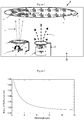
- Figure 1 is a schematic drawing of modified PIAD with a reverse mask and a side shield that enabled the deposition of thick MgO-MgF2 composited films or coatings that are also simultaneously densified.
- Figure 1 illustrates a deposition set-up 8 having a vacuum chamber 28 in which is located a substrate carrier 22 having substrates 24 thereon, an e-beam 10 that impinges a target 18 to produce a vapor flux 20 that passes through a reversed mask 12 for deposition on the substrates 24.
- a plasma source 16 that generates a plasma 21, for example an argon plasma, and an oxygen source/feed for producing the plasma as an oxygen containing plasma.
- the film densification process is controlled by means of masking technology as shown in Figure 1 , where zone ⁇ and ⁇ correspond to the mask shadowed and un-shadowed areas, respectively.
- P ⁇ represents in-situ plasma smoothing
- P ⁇ corresponds to plasma ion-assisted deposition.
- V b is the bias voltage
- J i and m i are the plasma ion flux in ion/(cm 2 sec)
- m i is mass in a.u., respectively.
- R is the coating deposition rate in nm/sec; e is the electron charge; ⁇ is a unit conversion factor; n s is surface atom density in atom/cm 2 ; and ⁇ and ⁇ are the radian of mask shadowed and un-shadowed area of the vapor flux relative to the center of the rotated plate having a rotation frequency of f .
- Adjustment of the mask shape and height, APS parameters, and plate rotation frequency enables one to separately control the amount of momentum transfer for fluorine depletion and for plasma assisted deposition.
- Oxygen gas, O 2 is introduced into the deposition system during the modified PIAD process to compensate fluorine loss and obtain MgO-MgF2 composited film.
- the oxygen flow rate is proportional to the deposition rate and the applied bias voltage, and can range from 3 sccm to 25 sccm depending on the deposition rate and bias voltage. It should be noted that in the process described herein a relatively high bias voltage of 110V was employed in the process.
- a low bias voltage of approximately 50V is necessary in order to eliminate the amount of fluorine depletion.
- a high bias voltage is intentionally applied for MgF 2 film modification in an oxygen rich plasma environment in order to form the MgO-MgF 2 coating.
- FIG. 2 is a graph of the refractive indices, n, of a 200nm modified MgO-MgF 2 coating as a function of wavelength.
- n the refractive index of a 200nm modified MgO-MgF 2 coating as a function of wavelength.
- a comparison of the refractive index at a wavelength of 2 ⁇ m, where most reference data is available, can be made for the modified MgO-MgF 2 coating versus bulk MgF 2 and MgO.
- the estimated refractive index of the modified MgO-MgF 2 film disclosed herein is 1.43.
- the refractive index of MgF 2 and MgO bulk materials at the same wavelength is 1.37 and 1.73, respectively ( Handbook of Chemistry and Physics, 48th ed. (The Chemical Rubber Co., Cleveland, OH, 1968) page B-192 ).
- fluorine depletion typically occurs when plasma interacts with the fluorides (see J. Wang et al, Extended lifetime of fluoride optics," 39th Bolder Damage Symposium, published as Proceedings of the SPIE 6720, 672011-9 (2009 ).
- the amount of fluorine depletion is strongly process dependent. Using a bias voltage of 110 V and a deposition rate of 0.25 nm/sec, it is reasonable to assume a maximum of 10% fluorine which is depleted during the MgF 2 modification process which results in the formation of a MgO-MgF 2 coating.
- MgO-MgF 2 composited coating Within an oxygen rich plasma environment, the depleted fluorine sites are replaced by oxygen, leading to the formation of MgO and resulting in a MgO-MgF 2 composited coating.
- An estimated refractive index of coating consisting of 10% MgO and 90% MgF 2 , the material being deposited using MgO and MgF 2 as coating source materials, at a wavelength of 2 ⁇ is 1.40, which is lower than the value of 1.43 for the modified MgO-MgF 2 film of the present disclosure in which only MgF 2 is the only metal-containing source material and oxygen is used to convert some of the MgF 2 to MgO.
- the additional increase in refractive index of the modified MgF 2 film may contribute to the fact that the PIAD process results in a high film packing density which is higher than the MgF 2 bulk material. Similar densification effect has been obtained in SiO 2 film ( J. Wang et al, "Elastic and plastic relaxation of densified SiO2 films," Applied Optics Vol. 47(13), pages 189-192 (2008 )).
- the modified MgF 2 film or coating is densified to form a MgO-MgF 2 composited coating or film, instead of a pure MgF 2 film or coating.
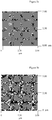
- FIGS. 3a and 3b show AFM images of 200nm MgO-MgF 2 composited film deposited by the modified PIAD process ( Figure 3a ) and a standard pure MgF 2 film with the same thickness ( Figure 3b ).
- the corresponding surface roughness for Figures 3a and 3b is 0.4nm and 2.4nm, respectively.
- the smoothed film structure of Figure 3a further increases coating durability, especially when it is used as a capping layer.
- a MgO-MgF 2 composited film for IR optics, especially for IR antireflective coatings where the modified MgO-MgF 2 composited film serves as a capping layer, leading to an increased abrasion resistance and environmental durability.
- a MgO-MgF 2 composited film can be used as a capping layer for a LWIR broadband AR application.
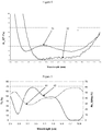
- Figure 4 plots a reflectance (Rx) at 12° angle of incidence of a LWIR broadband AR coating without the MgO-MgF 2 composited capping layer (numeral 30); and with the MgO-MgF2 composited capping coating layer (numeral 32).
- the reflectance of the an optic having the MgO-MgF 2 composited capping coating layer is less than 2% in the wavelength range of 7.25nm to 11.75nm as shown in Figure 4 . In the wavelength range of 7.5nm to 11.5nm the reflectance Rx is less than 1%. In contrast, the reflectance of a coating without the MgO-MgF 2 composited capping coating layer is greater than 2% in the same wavelength.
- Figure 5 plots the spectral transmittance Tx (numeral 40) and reflectance Rx_12° (numeral 42) of the LWIR broadband AR coating with the MgO-MgF 2 composited layer 30 as a capping layer.
- the reflectance Rx is less than 2% in the approximate range of 7.25nm to 11.25nm, and the transmission Tx is greater than 60% in the same wavelength range.
- the LWIR broadband AR without the capping layer fails severe abrasion test describe elsewhere herein.
- the durability of the MgO-MgF 2 composited AR coating increases with the use of a 700nm MgO-MgF 2 composited capping layer.
- a witness sample prepared as described here with a 700nm MgO-MgF 2 composited capping layer passed all severe abrasion tests and environmental tests using MIL-C-48497A.
- an optic having a composited MgO-MgF 2 anti-reflective coating thereon suitable for use with infrared radiation having a wavelength in the range of 1 ⁇ m to 14 ⁇ m, said coating thickness being variable with said wavelength range, the coating thickness being in the range of 100nm to 1500nm.
- the coating thickness can be in the range of 150nm to 300nm.
- the coating thickness can be in the range of 250nm to 450nm.
- the coating thickness can be in the range of 600nm to 1500nm.
- the coating can have a reflectance Rx of less than 2% in the wavelength range of 7.25nm to 11.75nm. Also, the coating can have a reflectance of less than 1% in the wavelength range of 7.5nm to 11.5nm. Further, the coated optic can have a transmission of greater than 60% in the wavelength range of 7.5nm to 11.5nm. In addition, the coating on the coated optic can pass an abrasion test with a barring force between 2 and 2.5 lbs.
- the disclosure is directed to a method of depositing a thin film of a selected material on the surface of a substrate using plasma ion assisted deposition, the method having the steps of: providing a vacuum chamber and within said chamber:
- the coating can be deposited to a thickness in the range of 100nm to 1500nm.
- the coating is deposited to a thickness in the range of 150nm to 300nm.
- the coating is deposited to a thickness in the range of 250nm to 450nm.
- the coating is deposited to a thickness in the range of 600nm to 1500nm.
- the coating material deposited on said substrate can pass an abrasion test with a barring force between 0.9072 and 1.1340 kg (2 and 2.5 lbs).
Landscapes
- Chemical & Material Sciences (AREA)
- Chemical Kinetics & Catalysis (AREA)
- Engineering & Computer Science (AREA)
- Materials Engineering (AREA)
- Mechanical Engineering (AREA)
- Metallurgy (AREA)
- Organic Chemistry (AREA)
- Physics & Mathematics (AREA)
- Inorganic Chemistry (AREA)
- General Physics & Mathematics (AREA)
- Optics & Photonics (AREA)
- Health & Medical Sciences (AREA)
- Toxicology (AREA)
- Physical Vapour Deposition (AREA)
- Surface Treatment Of Optical Elements (AREA)
- Optical Elements Other Than Lenses (AREA)
- Optical Filters (AREA)
Applications Claiming Priority (2)
| Application Number | Priority Date | Filing Date | Title |
|---|---|---|---|
| US201161491667P | 2011-05-31 | 2011-05-31 | |
| PCT/US2012/039230 WO2012166484A1 (en) | 2011-05-31 | 2012-05-24 | DURABLE MgO-MgF2 COMPOSITE FILM FOR INFRARED ANTI-REFLECTION COATINGS |
Publications (2)
| Publication Number | Publication Date |
|---|---|
| EP2715412A1 EP2715412A1 (en) | 2014-04-09 |
| EP2715412B1 true EP2715412B1 (en) | 2019-09-04 |
Family
ID=46201852
Family Applications (1)
| Application Number | Title | Priority Date | Filing Date |
|---|---|---|---|
| EP12725241.9A Active EP2715412B1 (en) | 2011-05-31 | 2012-05-24 | DURABLE MgO-MgF2 COMPOSITE FILM FOR INFRARED ANTI-REFLECTION COATINGS |
Country Status (4)
| Country | Link |
|---|---|
| US (2) | US20120307353A1 (enExample) |
| EP (1) | EP2715412B1 (enExample) |
| JP (2) | JP2015501001A (enExample) |
| WO (1) | WO2012166484A1 (enExample) |
Families Citing this family (5)
| Publication number | Priority date | Publication date | Assignee | Title |
|---|---|---|---|---|
| US10502965B2 (en) | 2014-09-17 | 2019-12-10 | Corning Incorporated | High-efficiency multiwavelength beam expander employing dielectric-enhanced mirrors |
| US20170066684A1 (en) * | 2015-09-08 | 2017-03-09 | Corning Incorporated | Optical coatings including buffer layers |
| US11572617B2 (en) * | 2016-05-03 | 2023-02-07 | Applied Materials, Inc. | Protective metal oxy-fluoride coatings |
| EP4220244A4 (en) * | 2020-09-23 | 2024-11-20 | Agc Inc. | Far-infrared ray transmitting member and method for manufacturing far-infrared ray transmitting member |
| DE102021206788A1 (de) * | 2021-06-30 | 2023-01-05 | Carl Zeiss Smt Gmbh | Verfahren zum Abscheiden einer Schicht, optisches Element und optische Anordnung für den DUV-Wellenlängenbereich |
Citations (2)
| Publication number | Priority date | Publication date | Assignee | Title |
|---|---|---|---|---|
| JP3625876B2 (ja) * | 1994-11-14 | 2005-03-02 | オリンパス株式会社 | 光学薄膜の製造方法および該光学薄膜を有する光学部品 |
| US20080050910A1 (en) * | 2006-08-25 | 2008-02-28 | Gary Allen Hart | Method for producing smooth, dense optical films |
Family Cites Families (26)
| Publication number | Priority date | Publication date | Assignee | Title |
|---|---|---|---|---|
| JPS5133751B2 (enExample) * | 1972-07-27 | 1976-09-21 | ||
| CH588711A5 (enExample) * | 1975-02-18 | 1977-06-15 | Balzers Patent Beteilig Ag | |
| US5165960A (en) * | 1991-07-29 | 1992-11-24 | Ford Motor Company | Deposition of magnesium fluoride films |
| JPH06313802A (ja) * | 1993-04-28 | 1994-11-08 | Topcon Corp | 赤外域多層膜 |
| JP3526922B2 (ja) * | 1994-10-14 | 2004-05-17 | 株式会社トプコン | 赤外反射防止膜 |
| JPH08310840A (ja) * | 1995-05-16 | 1996-11-26 | Nippon Sheet Glass Co Ltd | 反射防止膜 |
| JP3987169B2 (ja) * | 1997-10-02 | 2007-10-03 | オリンパス株式会社 | 光学薄膜の製造方法 |
| JPH10282304A (ja) * | 1998-05-22 | 1998-10-23 | Nikon Corp | 光学薄膜 |
| TW469465B (en) * | 1998-12-10 | 2001-12-21 | Mitsubishi Materials Corp | Protective film for FPD and manufacture thereof, and FPD using the same |
| EP1134303B1 (en) | 2000-03-13 | 2010-06-09 | Canon Kabushiki Kaisha | Thin film production process |
| JP3639795B2 (ja) * | 2000-03-13 | 2005-04-20 | キヤノン株式会社 | 薄膜の製造方法 |
| JP2001262317A (ja) * | 2000-03-17 | 2001-09-26 | Olympus Optical Co Ltd | 光学薄膜及びその製造方法 |
| JP4184706B2 (ja) * | 2002-04-30 | 2008-11-19 | 浜松ホトニクス株式会社 | 反射防止膜の製造方法 |
| JP2005281726A (ja) * | 2004-03-26 | 2005-10-13 | Ntt Afty Corp | プラズマ成膜方法及びその装置 |
| JP2006065140A (ja) * | 2004-08-30 | 2006-03-09 | Canon Inc | 反射防止膜、当該反射防止膜を有する光学系、露光装置、並びに、デバイス製造方法 |
| EP1965229A3 (en) | 2007-02-28 | 2008-12-10 | Corning Incorporated | Engineered fluoride-coated elements for laser systems |
| WO2009070227A1 (en) * | 2007-11-30 | 2009-06-04 | Corning Incorporated | Dense homogeneous fluoride films for duv elements and method of preparing same |
| US20110111131A1 (en) * | 2008-03-27 | 2011-05-12 | Fraunhofer-Gesellschaft Zur Forderung Der Angewandten Forschung E.V. | Method for producing a multicomponent, polymer- and metal-containing layer system, device and coated article |
| US20110014398A1 (en) * | 2008-04-09 | 2011-01-20 | Ulvac, Inc. | Film deposition apparatus and film deposition method |
| US8399110B2 (en) | 2008-05-29 | 2013-03-19 | Corning Incorporated | Adhesive, hermetic oxide films for metal fluoride optics and method of making same |
| US8526293B2 (en) * | 2008-06-13 | 2013-09-03 | Panasonic Corporation | Information recording medium and recording/reproducing method for the same |
| US8153241B2 (en) | 2009-02-26 | 2012-04-10 | Corning Incorporated | Wide-angle highly reflective mirrors at 193NM |
| US8382823B2 (en) * | 2009-05-28 | 2013-02-26 | Snu R&Db Foundation | Biodegradable stent and method for manufacturing the same |
| US8526104B2 (en) | 2010-04-30 | 2013-09-03 | Corning Incorporated | Plasma ion assisted deposition of Mo/Si multilayer EUV coatings |
| JP5932251B2 (ja) * | 2011-06-17 | 2016-06-08 | キヤノン株式会社 | フッ化膜形成方法及び光学素子の製造方法 |
| US20140154510A1 (en) * | 2011-07-11 | 2014-06-05 | Panasonic Corporation | Film structure and method for producing same |
-
2012
- 2012-05-18 US US13/475,009 patent/US20120307353A1/en not_active Abandoned
- 2012-05-24 EP EP12725241.9A patent/EP2715412B1/en active Active
- 2012-05-24 JP JP2014513578A patent/JP2015501001A/ja active Pending
- 2012-05-24 WO PCT/US2012/039230 patent/WO2012166484A1/en not_active Ceased
-
2017
- 2017-01-06 JP JP2017001061A patent/JP6381687B2/ja not_active Expired - Fee Related
- 2017-03-06 US US15/450,647 patent/US9963773B2/en active Active
Patent Citations (2)
| Publication number | Priority date | Publication date | Assignee | Title |
|---|---|---|---|---|
| JP3625876B2 (ja) * | 1994-11-14 | 2005-03-02 | オリンパス株式会社 | 光学薄膜の製造方法および該光学薄膜を有する光学部品 |
| US20080050910A1 (en) * | 2006-08-25 | 2008-02-28 | Gary Allen Hart | Method for producing smooth, dense optical films |
Also Published As
| Publication number | Publication date |
|---|---|
| US20120307353A1 (en) | 2012-12-06 |
| JP2015501001A (ja) | 2015-01-08 |
| US9963773B2 (en) | 2018-05-08 |
| WO2012166484A1 (en) | 2012-12-06 |
| US20170175245A1 (en) | 2017-06-22 |
| EP2715412A1 (en) | 2014-04-09 |
| JP2017095805A (ja) | 2017-06-01 |
| JP6381687B2 (ja) | 2018-08-29 |
Similar Documents
| Publication | Publication Date | Title |
|---|---|---|
| US9963773B2 (en) | Durable MgO—MgF2 composite film for infrared anti-reflection coatings | |
| EP1232407B1 (fr) | Filtre anticalorique et procede de fabrication de ce filtre | |
| US8153241B2 (en) | Wide-angle highly reflective mirrors at 193NM | |
| JP5622468B2 (ja) | レンズの製造方法及びレンズ | |
| US9983333B2 (en) | Hafnium or zirconium oxide coating | |
| US8817367B2 (en) | Plasma ion assisted deposition of Mo/Si multilayer EUV coatings | |
| EP1529124B1 (fr) | Procede d'obtention d'une couche mince de silice fluoree stabilisee, substrat ainsi revetu et lentille ophthalmique ainsi obtenue | |
| EP3751319A1 (en) | Optical thin film, optical member, and method for manufacturing optical thin film | |
| KR102403855B1 (ko) | 내구성 개선을 위한 나노-라미네이트를 가진 광학 코팅 | |
| EP3757626B1 (en) | Optical device and manufacturing method therefor | |
| JP5916821B2 (ja) | 酸化ハフニウムコーティング | |
| US5879820A (en) | Multilayer stack of fluoride materials usable in optics and its production process | |
| EP3055265A1 (fr) | Vitrage de contrôle thermique | |
| WO1997008357A1 (en) | Anti-reflective coating | |
| EP1211523A2 (en) | Infrared laser optical element and manufacturing method therefor | |
| JP7216471B2 (ja) | 車載レンズ用のプラスチックレンズ及びその製造方法 | |
| JP2015505900A (ja) | 中赤外線性能が改善された酸化イットリウム被覆光学素子 | |
| EP3605154B1 (en) | Thin film forming method and porous thin film | |
| Amochkina et al. | Characterization of PARMS Produced 1-μm thick Ta2O5 and SiO2 Monolayers in 0.35-5 μm Spectral Range | |
| JPH09202961A (ja) | 赤外線用光学膜の製造方法 | |
| JPH08333672A (ja) | 光学部品の製造方法 | |
| WO2023042438A1 (ja) | 遮光膜、多層反射防止膜、それらの製造方法及び光学部材 | |
| Hirvonen | Ion Beam Assisted Deposition for Optical Coatings: R&D to Production | |
| JPH03218822A (ja) | 紫外線遮断ガラス | |
| JPH0763903A (ja) | プラスチック製光学部品の光学薄膜およびその成膜方法 |
Legal Events
| Date | Code | Title | Description |
|---|---|---|---|
| PUAI | Public reference made under article 153(3) epc to a published international application that has entered the european phase |
Free format text: ORIGINAL CODE: 0009012 |
|
| 17P | Request for examination filed |
Effective date: 20131111 |
|
| AK | Designated contracting states |
Kind code of ref document: A1 Designated state(s): AL AT BE BG CH CY CZ DE DK EE ES FI FR GB GR HR HU IE IS IT LI LT LU LV MC MK MT NL NO PL PT RO RS SE SI SK SM TR |
|
| DAX | Request for extension of the european patent (deleted) | ||
| STAA | Information on the status of an ep patent application or granted ep patent |
Free format text: STATUS: EXAMINATION IS IN PROGRESS |
|
| 17Q | First examination report despatched |
Effective date: 20180606 |
|
| GRAP | Despatch of communication of intention to grant a patent |
Free format text: ORIGINAL CODE: EPIDOSNIGR1 |
|
| STAA | Information on the status of an ep patent application or granted ep patent |
Free format text: STATUS: GRANT OF PATENT IS INTENDED |
|
| INTG | Intention to grant announced |
Effective date: 20190624 |
|
| GRAS | Grant fee paid |
Free format text: ORIGINAL CODE: EPIDOSNIGR3 |
|
| GRAA | (expected) grant |
Free format text: ORIGINAL CODE: 0009210 |
|
| STAA | Information on the status of an ep patent application or granted ep patent |
Free format text: STATUS: THE PATENT HAS BEEN GRANTED |
|
| AK | Designated contracting states |
Kind code of ref document: B1 Designated state(s): AL AT BE BG CH CY CZ DE DK EE ES FI FR GB GR HR HU IE IS IT LI LT LU LV MC MK MT NL NO PL PT RO RS SE SI SK SM TR |
|
| REG | Reference to a national code |
Ref country code: GB Ref legal event code: FG4D |
|
| REG | Reference to a national code |
Ref country code: CH Ref legal event code: EP |
|
| REG | Reference to a national code |
Ref country code: AT Ref legal event code: REF Ref document number: 1176152 Country of ref document: AT Kind code of ref document: T Effective date: 20190915 |
|
| REG | Reference to a national code |
Ref country code: DE Ref legal event code: R096 Ref document number: 602012063609 Country of ref document: DE |
|
| REG | Reference to a national code |
Ref country code: IE Ref legal event code: FG4D |
|
| REG | Reference to a national code |
Ref country code: NL Ref legal event code: FP |
|
| REG | Reference to a national code |
Ref country code: LT Ref legal event code: MG4D |
|
| PG25 | Lapsed in a contracting state [announced via postgrant information from national office to epo] |
Ref country code: NO Free format text: LAPSE BECAUSE OF FAILURE TO SUBMIT A TRANSLATION OF THE DESCRIPTION OR TO PAY THE FEE WITHIN THE PRESCRIBED TIME-LIMIT Effective date: 20191204 Ref country code: FI Free format text: LAPSE BECAUSE OF FAILURE TO SUBMIT A TRANSLATION OF THE DESCRIPTION OR TO PAY THE FEE WITHIN THE PRESCRIBED TIME-LIMIT Effective date: 20190904 Ref country code: SE Free format text: LAPSE BECAUSE OF FAILURE TO SUBMIT A TRANSLATION OF THE DESCRIPTION OR TO PAY THE FEE WITHIN THE PRESCRIBED TIME-LIMIT Effective date: 20190904 Ref country code: BG Free format text: LAPSE BECAUSE OF FAILURE TO SUBMIT A TRANSLATION OF THE DESCRIPTION OR TO PAY THE FEE WITHIN THE PRESCRIBED TIME-LIMIT Effective date: 20191204 Ref country code: HR Free format text: LAPSE BECAUSE OF FAILURE TO SUBMIT A TRANSLATION OF THE DESCRIPTION OR TO PAY THE FEE WITHIN THE PRESCRIBED TIME-LIMIT Effective date: 20190904 Ref country code: LT Free format text: LAPSE BECAUSE OF FAILURE TO SUBMIT A TRANSLATION OF THE DESCRIPTION OR TO PAY THE FEE WITHIN THE PRESCRIBED TIME-LIMIT Effective date: 20190904 |
|
| PG25 | Lapsed in a contracting state [announced via postgrant information from national office to epo] |
Ref country code: AL Free format text: LAPSE BECAUSE OF FAILURE TO SUBMIT A TRANSLATION OF THE DESCRIPTION OR TO PAY THE FEE WITHIN THE PRESCRIBED TIME-LIMIT Effective date: 20190904 Ref country code: LV Free format text: LAPSE BECAUSE OF FAILURE TO SUBMIT A TRANSLATION OF THE DESCRIPTION OR TO PAY THE FEE WITHIN THE PRESCRIBED TIME-LIMIT Effective date: 20190904 Ref country code: RS Free format text: LAPSE BECAUSE OF FAILURE TO SUBMIT A TRANSLATION OF THE DESCRIPTION OR TO PAY THE FEE WITHIN THE PRESCRIBED TIME-LIMIT Effective date: 20190904 Ref country code: GR Free format text: LAPSE BECAUSE OF FAILURE TO SUBMIT A TRANSLATION OF THE DESCRIPTION OR TO PAY THE FEE WITHIN THE PRESCRIBED TIME-LIMIT Effective date: 20191205 Ref country code: ES Free format text: LAPSE BECAUSE OF FAILURE TO SUBMIT A TRANSLATION OF THE DESCRIPTION OR TO PAY THE FEE WITHIN THE PRESCRIBED TIME-LIMIT Effective date: 20190904 |
|
| REG | Reference to a national code |
Ref country code: AT Ref legal event code: MK05 Ref document number: 1176152 Country of ref document: AT Kind code of ref document: T Effective date: 20190904 |
|
| PG25 | Lapsed in a contracting state [announced via postgrant information from national office to epo] |
Ref country code: RO Free format text: LAPSE BECAUSE OF FAILURE TO SUBMIT A TRANSLATION OF THE DESCRIPTION OR TO PAY THE FEE WITHIN THE PRESCRIBED TIME-LIMIT Effective date: 20190904 Ref country code: PL Free format text: LAPSE BECAUSE OF FAILURE TO SUBMIT A TRANSLATION OF THE DESCRIPTION OR TO PAY THE FEE WITHIN THE PRESCRIBED TIME-LIMIT Effective date: 20190904 Ref country code: PT Free format text: LAPSE BECAUSE OF FAILURE TO SUBMIT A TRANSLATION OF THE DESCRIPTION OR TO PAY THE FEE WITHIN THE PRESCRIBED TIME-LIMIT Effective date: 20200106 Ref country code: IT Free format text: LAPSE BECAUSE OF FAILURE TO SUBMIT A TRANSLATION OF THE DESCRIPTION OR TO PAY THE FEE WITHIN THE PRESCRIBED TIME-LIMIT Effective date: 20190904 Ref country code: AT Free format text: LAPSE BECAUSE OF FAILURE TO SUBMIT A TRANSLATION OF THE DESCRIPTION OR TO PAY THE FEE WITHIN THE PRESCRIBED TIME-LIMIT Effective date: 20190904 Ref country code: EE Free format text: LAPSE BECAUSE OF FAILURE TO SUBMIT A TRANSLATION OF THE DESCRIPTION OR TO PAY THE FEE WITHIN THE PRESCRIBED TIME-LIMIT Effective date: 20190904 |
|
| PG25 | Lapsed in a contracting state [announced via postgrant information from national office to epo] |
Ref country code: CZ Free format text: LAPSE BECAUSE OF FAILURE TO SUBMIT A TRANSLATION OF THE DESCRIPTION OR TO PAY THE FEE WITHIN THE PRESCRIBED TIME-LIMIT Effective date: 20190904 Ref country code: SM Free format text: LAPSE BECAUSE OF FAILURE TO SUBMIT A TRANSLATION OF THE DESCRIPTION OR TO PAY THE FEE WITHIN THE PRESCRIBED TIME-LIMIT Effective date: 20190904 Ref country code: IS Free format text: LAPSE BECAUSE OF FAILURE TO SUBMIT A TRANSLATION OF THE DESCRIPTION OR TO PAY THE FEE WITHIN THE PRESCRIBED TIME-LIMIT Effective date: 20200224 Ref country code: SK Free format text: LAPSE BECAUSE OF FAILURE TO SUBMIT A TRANSLATION OF THE DESCRIPTION OR TO PAY THE FEE WITHIN THE PRESCRIBED TIME-LIMIT Effective date: 20190904 |
|
| REG | Reference to a national code |
Ref country code: DE Ref legal event code: R097 Ref document number: 602012063609 Country of ref document: DE |
|
| PLBE | No opposition filed within time limit |
Free format text: ORIGINAL CODE: 0009261 |
|
| STAA | Information on the status of an ep patent application or granted ep patent |
Free format text: STATUS: NO OPPOSITION FILED WITHIN TIME LIMIT |
|
| PG2D | Information on lapse in contracting state deleted |
Ref country code: IS |
|
| PG25 | Lapsed in a contracting state [announced via postgrant information from national office to epo] |
Ref country code: DK Free format text: LAPSE BECAUSE OF FAILURE TO SUBMIT A TRANSLATION OF THE DESCRIPTION OR TO PAY THE FEE WITHIN THE PRESCRIBED TIME-LIMIT Effective date: 20190904 Ref country code: IS Free format text: LAPSE BECAUSE OF FAILURE TO SUBMIT A TRANSLATION OF THE DESCRIPTION OR TO PAY THE FEE WITHIN THE PRESCRIBED TIME-LIMIT Effective date: 20200105 |
|
| 26N | No opposition filed |
Effective date: 20200605 |
|
| PG25 | Lapsed in a contracting state [announced via postgrant information from national office to epo] |
Ref country code: SI Free format text: LAPSE BECAUSE OF FAILURE TO SUBMIT A TRANSLATION OF THE DESCRIPTION OR TO PAY THE FEE WITHIN THE PRESCRIBED TIME-LIMIT Effective date: 20190904 |
|
| PG25 | Lapsed in a contracting state [announced via postgrant information from national office to epo] |
Ref country code: MC Free format text: LAPSE BECAUSE OF FAILURE TO SUBMIT A TRANSLATION OF THE DESCRIPTION OR TO PAY THE FEE WITHIN THE PRESCRIBED TIME-LIMIT Effective date: 20190904 Ref country code: CH Free format text: LAPSE BECAUSE OF NON-PAYMENT OF DUE FEES Effective date: 20200531 Ref country code: LI Free format text: LAPSE BECAUSE OF NON-PAYMENT OF DUE FEES Effective date: 20200531 |
|
| REG | Reference to a national code |
Ref country code: BE Ref legal event code: MM Effective date: 20200531 |
|
| GBPC | Gb: european patent ceased through non-payment of renewal fee |
Effective date: 20200524 |
|
| PG25 | Lapsed in a contracting state [announced via postgrant information from national office to epo] |
Ref country code: LU Free format text: LAPSE BECAUSE OF NON-PAYMENT OF DUE FEES Effective date: 20200524 |
|
| PG25 | Lapsed in a contracting state [announced via postgrant information from national office to epo] |
Ref country code: IE Free format text: LAPSE BECAUSE OF NON-PAYMENT OF DUE FEES Effective date: 20200524 Ref country code: FR Free format text: LAPSE BECAUSE OF NON-PAYMENT OF DUE FEES Effective date: 20200531 Ref country code: GB Free format text: LAPSE BECAUSE OF NON-PAYMENT OF DUE FEES Effective date: 20200524 |
|
| PG25 | Lapsed in a contracting state [announced via postgrant information from national office to epo] |
Ref country code: BE Free format text: LAPSE BECAUSE OF NON-PAYMENT OF DUE FEES Effective date: 20200531 |
|
| PG25 | Lapsed in a contracting state [announced via postgrant information from national office to epo] |
Ref country code: TR Free format text: LAPSE BECAUSE OF FAILURE TO SUBMIT A TRANSLATION OF THE DESCRIPTION OR TO PAY THE FEE WITHIN THE PRESCRIBED TIME-LIMIT Effective date: 20190904 Ref country code: MT Free format text: LAPSE BECAUSE OF FAILURE TO SUBMIT A TRANSLATION OF THE DESCRIPTION OR TO PAY THE FEE WITHIN THE PRESCRIBED TIME-LIMIT Effective date: 20190904 Ref country code: CY Free format text: LAPSE BECAUSE OF FAILURE TO SUBMIT A TRANSLATION OF THE DESCRIPTION OR TO PAY THE FEE WITHIN THE PRESCRIBED TIME-LIMIT Effective date: 20190904 |
|
| PG25 | Lapsed in a contracting state [announced via postgrant information from national office to epo] |
Ref country code: MK Free format text: LAPSE BECAUSE OF FAILURE TO SUBMIT A TRANSLATION OF THE DESCRIPTION OR TO PAY THE FEE WITHIN THE PRESCRIBED TIME-LIMIT Effective date: 20190904 |
|
| P01 | Opt-out of the competence of the unified patent court (upc) registered |
Effective date: 20230527 |
|
| PGFP | Annual fee paid to national office [announced via postgrant information from national office to epo] |
Ref country code: NL Payment date: 20250421 Year of fee payment: 14 |
|
| PGFP | Annual fee paid to national office [announced via postgrant information from national office to epo] |
Ref country code: DE Payment date: 20250409 Year of fee payment: 14 |