EP2701325A1 - Procédé de génération de signal et dispositif de génération de signal - Google Patents
Procédé de génération de signal et dispositif de génération de signal Download PDFInfo
- Publication number
- EP2701325A1 EP2701325A1 EP12773614.8A EP12773614A EP2701325A1 EP 2701325 A1 EP2701325 A1 EP 2701325A1 EP 12773614 A EP12773614 A EP 12773614A EP 2701325 A1 EP2701325 A1 EP 2701325A1
- Authority
- EP
- European Patent Office
- Prior art keywords
- phase
- signal
- data
- change
- symbols
- Prior art date
- Legal status (The legal status is an assumption and is not a legal conclusion. Google has not performed a legal analysis and makes no representation as to the accuracy of the status listed.)
- Granted
Links
- 238000000034 method Methods 0.000 title claims abstract description 100
- 230000008859 change Effects 0.000 claims abstract description 941
- 230000005540 biological transmission Effects 0.000 claims abstract description 676
- 239000011159 matrix material Substances 0.000 claims abstract description 129
- 230000007274 generation of a signal involved in cell-cell signaling Effects 0.000 claims abstract description 33
- 230000008569 process Effects 0.000 claims description 26
- 238000012545 processing Methods 0.000 abstract description 152
- 238000012937 correction Methods 0.000 description 145
- 238000013507 mapping Methods 0.000 description 119
- 238000004891 communication Methods 0.000 description 109
- 238000001514 detection method Methods 0.000 description 100
- 235000007682 pyridoxal 5'-phosphate Nutrition 0.000 description 71
- 230000000694 effects Effects 0.000 description 64
- NGVDGCNFYWLIFO-UHFFFAOYSA-N pyridoxal 5'-phosphate Chemical compound CC1=NC=C(COP(O)(O)=O)C(C=O)=C1O NGVDGCNFYWLIFO-UHFFFAOYSA-N 0.000 description 60
- 238000006243 chemical reaction Methods 0.000 description 52
- 238000009826 distribution Methods 0.000 description 40
- 239000000969 carrier Substances 0.000 description 28
- 125000004122 cyclic group Chemical group 0.000 description 28
- 230000003321 amplification Effects 0.000 description 22
- 239000000284 extract Substances 0.000 description 22
- 238000003199 nucleic acid amplification method Methods 0.000 description 22
- 238000003780 insertion Methods 0.000 description 21
- 230000037431 insertion Effects 0.000 description 21
- 239000002609 medium Substances 0.000 description 18
- 238000004364 calculation method Methods 0.000 description 17
- 230000006870 function Effects 0.000 description 16
- 230000006872 improvement Effects 0.000 description 16
- 238000001824 photoionisation detection Methods 0.000 description 16
- 239000000047 product Substances 0.000 description 16
- 230000015556 catabolic process Effects 0.000 description 15
- 238000006731 degradation reaction Methods 0.000 description 15
- 239000013598 vector Substances 0.000 description 15
- 230000009467 reduction Effects 0.000 description 14
- 238000010586 diagram Methods 0.000 description 13
- 238000005516 engineering process Methods 0.000 description 13
- 230000002829 reductive effect Effects 0.000 description 11
- 238000001228 spectrum Methods 0.000 description 10
- 239000013589 supplement Substances 0.000 description 10
- 230000001419 dependent effect Effects 0.000 description 8
- 238000002360 preparation method Methods 0.000 description 8
- 101100228469 Caenorhabditis elegans exp-1 gene Proteins 0.000 description 7
- 230000002452 interceptive effect Effects 0.000 description 7
- 238000012986 modification Methods 0.000 description 7
- 230000004048 modification Effects 0.000 description 7
- 230000000737 periodic effect Effects 0.000 description 7
- 238000004422 calculation algorithm Methods 0.000 description 6
- 230000011664 signaling Effects 0.000 description 6
- 238000005562 fading Methods 0.000 description 5
- 239000004065 semiconductor Substances 0.000 description 5
- 230000005236 sound signal Effects 0.000 description 5
- OVSKIKFHRZPJSS-UHFFFAOYSA-N 2,4-D Chemical compound OC(=O)COC1=CC=C(Cl)C=C1Cl OVSKIKFHRZPJSS-UHFFFAOYSA-N 0.000 description 4
- VZSRBBMJRBPUNF-UHFFFAOYSA-N 2-(2,3-dihydro-1H-inden-2-ylamino)-N-[3-oxo-3-(2,4,6,7-tetrahydrotriazolo[4,5-c]pyridin-5-yl)propyl]pyrimidine-5-carboxamide Chemical compound C1C(CC2=CC=CC=C12)NC1=NC=C(C=N1)C(=O)NCCC(N1CC2=C(CC1)NN=N2)=O VZSRBBMJRBPUNF-UHFFFAOYSA-N 0.000 description 4
- AFCARXCZXQIEQB-UHFFFAOYSA-N N-[3-oxo-3-(2,4,6,7-tetrahydrotriazolo[4,5-c]pyridin-5-yl)propyl]-2-[[3-(trifluoromethoxy)phenyl]methylamino]pyrimidine-5-carboxamide Chemical compound O=C(CCNC(=O)C=1C=NC(=NC=1)NCC1=CC(=CC=C1)OC(F)(F)F)N1CC2=C(CC1)NN=N2 AFCARXCZXQIEQB-UHFFFAOYSA-N 0.000 description 4
- 238000013459 approach Methods 0.000 description 4
- 238000007906 compression Methods 0.000 description 4
- 230000006835 compression Effects 0.000 description 4
- 230000007850 degeneration Effects 0.000 description 4
- 238000001914 filtration Methods 0.000 description 4
- 230000000644 propagated effect Effects 0.000 description 4
- IHCCLXNEEPMSIO-UHFFFAOYSA-N 2-[4-[2-(2,3-dihydro-1H-inden-2-ylamino)pyrimidin-5-yl]piperidin-1-yl]-1-(2,4,6,7-tetrahydrotriazolo[4,5-c]pyridin-5-yl)ethanone Chemical compound C1C(CC2=CC=CC=C12)NC1=NC=C(C=N1)C1CCN(CC1)CC(=O)N1CC2=C(CC1)NN=N2 IHCCLXNEEPMSIO-UHFFFAOYSA-N 0.000 description 3
- NIPNSKYNPDTRPC-UHFFFAOYSA-N N-[2-oxo-2-(2,4,6,7-tetrahydrotriazolo[4,5-c]pyridin-5-yl)ethyl]-2-[[3-(trifluoromethoxy)phenyl]methylamino]pyrimidine-5-carboxamide Chemical compound O=C(CNC(=O)C=1C=NC(=NC=1)NCC1=CC(=CC=C1)OC(F)(F)F)N1CC2=C(CC1)NN=N2 NIPNSKYNPDTRPC-UHFFFAOYSA-N 0.000 description 3
- 230000010363 phase shift Effects 0.000 description 3
- 238000012805 post-processing Methods 0.000 description 3
- 238000000926 separation method Methods 0.000 description 3
- 238000003860 storage Methods 0.000 description 3
- XDLMVUHYZWKMMD-UHFFFAOYSA-N 3-trimethoxysilylpropyl 2-methylprop-2-enoate Chemical compound CO[Si](OC)(OC)CCCOC(=O)C(C)=C XDLMVUHYZWKMMD-UHFFFAOYSA-N 0.000 description 2
- 230000008901 benefit Effects 0.000 description 2
- 239000003638 chemical reducing agent Substances 0.000 description 2
- 238000000354 decomposition reaction Methods 0.000 description 2
- 230000001934 delay Effects 0.000 description 2
- 238000009432 framing Methods 0.000 description 2
- 230000010354 integration Effects 0.000 description 2
- 230000000670 limiting effect Effects 0.000 description 2
- 239000003607 modifier Substances 0.000 description 2
- 230000003287 optical effect Effects 0.000 description 2
- 230000009897 systematic effect Effects 0.000 description 2
- 238000012546 transfer Methods 0.000 description 2
- 239000006163 transport media Substances 0.000 description 2
- 238000011144 upstream manufacturing Methods 0.000 description 2
- OHVLMTFVQDZYHP-UHFFFAOYSA-N 1-(2,4,6,7-tetrahydrotriazolo[4,5-c]pyridin-5-yl)-2-[4-[2-[[3-(trifluoromethoxy)phenyl]methylamino]pyrimidin-5-yl]piperazin-1-yl]ethanone Chemical compound N1N=NC=2CN(CCC=21)C(CN1CCN(CC1)C=1C=NC(=NC=1)NCC1=CC(=CC=C1)OC(F)(F)F)=O OHVLMTFVQDZYHP-UHFFFAOYSA-N 0.000 description 1
- KZEVSDGEBAJOTK-UHFFFAOYSA-N 1-(2,4,6,7-tetrahydrotriazolo[4,5-c]pyridin-5-yl)-2-[5-[2-[[3-(trifluoromethoxy)phenyl]methylamino]pyrimidin-5-yl]-1,3,4-oxadiazol-2-yl]ethanone Chemical compound N1N=NC=2CN(CCC=21)C(CC=1OC(=NN=1)C=1C=NC(=NC=1)NCC1=CC(=CC=C1)OC(F)(F)F)=O KZEVSDGEBAJOTK-UHFFFAOYSA-N 0.000 description 1
- HMUNWXXNJPVALC-UHFFFAOYSA-N 1-[4-[2-(2,3-dihydro-1H-inden-2-ylamino)pyrimidin-5-yl]piperazin-1-yl]-2-(2,4,6,7-tetrahydrotriazolo[4,5-c]pyridin-5-yl)ethanone Chemical compound C1C(CC2=CC=CC=C12)NC1=NC=C(C=N1)N1CCN(CC1)C(CN1CC2=C(CC1)NN=N2)=O HMUNWXXNJPVALC-UHFFFAOYSA-N 0.000 description 1
- LDXJRKWFNNFDSA-UHFFFAOYSA-N 2-(2,4,6,7-tetrahydrotriazolo[4,5-c]pyridin-5-yl)-1-[4-[2-[[3-(trifluoromethoxy)phenyl]methylamino]pyrimidin-5-yl]piperazin-1-yl]ethanone Chemical compound C1CN(CC2=NNN=C21)CC(=O)N3CCN(CC3)C4=CN=C(N=C4)NCC5=CC(=CC=C5)OC(F)(F)F LDXJRKWFNNFDSA-UHFFFAOYSA-N 0.000 description 1
- WZFUQSJFWNHZHM-UHFFFAOYSA-N 2-[4-[2-(2,3-dihydro-1H-inden-2-ylamino)pyrimidin-5-yl]piperazin-1-yl]-1-(2,4,6,7-tetrahydrotriazolo[4,5-c]pyridin-5-yl)ethanone Chemical compound C1C(CC2=CC=CC=C12)NC1=NC=C(C=N1)N1CCN(CC1)CC(=O)N1CC2=C(CC1)NN=N2 WZFUQSJFWNHZHM-UHFFFAOYSA-N 0.000 description 1
- JQMFQLVAJGZSQS-UHFFFAOYSA-N 2-[4-[2-(2,3-dihydro-1H-inden-2-ylamino)pyrimidin-5-yl]piperazin-1-yl]-N-(2-oxo-3H-1,3-benzoxazol-6-yl)acetamide Chemical compound C1C(CC2=CC=CC=C12)NC1=NC=C(C=N1)N1CCN(CC1)CC(=O)NC1=CC2=C(NC(O2)=O)C=C1 JQMFQLVAJGZSQS-UHFFFAOYSA-N 0.000 description 1
- YJLUBHOZZTYQIP-UHFFFAOYSA-N 2-[5-[2-(2,3-dihydro-1H-inden-2-ylamino)pyrimidin-5-yl]-1,3,4-oxadiazol-2-yl]-1-(2,4,6,7-tetrahydrotriazolo[4,5-c]pyridin-5-yl)ethanone Chemical compound C1C(CC2=CC=CC=C12)NC1=NC=C(C=N1)C1=NN=C(O1)CC(=O)N1CC2=C(CC1)NN=N2 YJLUBHOZZTYQIP-UHFFFAOYSA-N 0.000 description 1
- YLZOPXRUQYQQID-UHFFFAOYSA-N 3-(2,4,6,7-tetrahydrotriazolo[4,5-c]pyridin-5-yl)-1-[4-[2-[[3-(trifluoromethoxy)phenyl]methylamino]pyrimidin-5-yl]piperazin-1-yl]propan-1-one Chemical compound N1N=NC=2CN(CCC=21)CCC(=O)N1CCN(CC1)C=1C=NC(=NC=1)NCC1=CC(=CC=C1)OC(F)(F)F YLZOPXRUQYQQID-UHFFFAOYSA-N 0.000 description 1
- CONKBQPVFMXDOV-QHCPKHFHSA-N 6-[(5S)-5-[[4-[2-(2,3-dihydro-1H-inden-2-ylamino)pyrimidin-5-yl]piperazin-1-yl]methyl]-2-oxo-1,3-oxazolidin-3-yl]-3H-1,3-benzoxazol-2-one Chemical compound C1C(CC2=CC=CC=C12)NC1=NC=C(C=N1)N1CCN(CC1)C[C@H]1CN(C(O1)=O)C1=CC2=C(NC(O2)=O)C=C1 CONKBQPVFMXDOV-QHCPKHFHSA-N 0.000 description 1
- DFGKGUXTPFWHIX-UHFFFAOYSA-N 6-[2-[4-[2-(2,3-dihydro-1H-inden-2-ylamino)pyrimidin-5-yl]piperazin-1-yl]acetyl]-3H-1,3-benzoxazol-2-one Chemical compound C1C(CC2=CC=CC=C12)NC1=NC=C(C=N1)N1CCN(CC1)CC(=O)C1=CC2=C(NC(O2)=O)C=C1 DFGKGUXTPFWHIX-UHFFFAOYSA-N 0.000 description 1
- 101000623895 Bos taurus Mucin-15 Proteins 0.000 description 1
- 235000008694 Humulus lupulus Nutrition 0.000 description 1
- 238000007476 Maximum Likelihood Methods 0.000 description 1
- 238000004458 analytical method Methods 0.000 description 1
- 238000013144 data compression Methods 0.000 description 1
- 238000013500 data storage Methods 0.000 description 1
- 238000013461 design Methods 0.000 description 1
- 230000005684 electric field Effects 0.000 description 1
- 230000008030 elimination Effects 0.000 description 1
- 238000003379 elimination reaction Methods 0.000 description 1
- 238000005265 energy consumption Methods 0.000 description 1
- 238000011156 evaluation Methods 0.000 description 1
- 230000004907 flux Effects 0.000 description 1
- 230000010365 information processing Effects 0.000 description 1
- 230000001788 irregular Effects 0.000 description 1
- 238000007726 management method Methods 0.000 description 1
- 238000002156 mixing Methods 0.000 description 1
- 238000005457 optimization Methods 0.000 description 1
- 238000012856 packing Methods 0.000 description 1
- 230000036961 partial effect Effects 0.000 description 1
- 238000003672 processing method Methods 0.000 description 1
- 230000008707 rearrangement Effects 0.000 description 1
- 230000004044 response Effects 0.000 description 1
- 230000002441 reversible effect Effects 0.000 description 1
- 238000005070 sampling Methods 0.000 description 1
- 238000007493 shaping process Methods 0.000 description 1
- 238000004088 simulation Methods 0.000 description 1
- 239000007787 solid Substances 0.000 description 1
- 230000006641 stabilisation Effects 0.000 description 1
- 238000011105 stabilization Methods 0.000 description 1
- 230000001502 supplementing effect Effects 0.000 description 1
- 230000001360 synchronised effect Effects 0.000 description 1
- 230000009466 transformation Effects 0.000 description 1
- 238000000844 transformation Methods 0.000 description 1
Images


Classifications
-
- H—ELECTRICITY
- H04—ELECTRIC COMMUNICATION TECHNIQUE
- H04B—TRANSMISSION
- H04B7/00—Radio transmission systems, i.e. using radiation field
- H04B7/02—Diversity systems; Multi-antenna system, i.e. transmission or reception using multiple antennas
- H04B7/04—Diversity systems; Multi-antenna system, i.e. transmission or reception using multiple antennas using two or more spaced independent antennas
- H04B7/0413—MIMO systems
-
- H—ELECTRICITY
- H04—ELECTRIC COMMUNICATION TECHNIQUE
- H04B—TRANSMISSION
- H04B7/00—Radio transmission systems, i.e. using radiation field
- H04B7/02—Diversity systems; Multi-antenna system, i.e. transmission or reception using multiple antennas
- H04B7/04—Diversity systems; Multi-antenna system, i.e. transmission or reception using multiple antennas using two or more spaced independent antennas
- H04B7/06—Diversity systems; Multi-antenna system, i.e. transmission or reception using multiple antennas using two or more spaced independent antennas at the transmitting station
- H04B7/0602—Diversity systems; Multi-antenna system, i.e. transmission or reception using multiple antennas using two or more spaced independent antennas at the transmitting station using antenna switching
-
- H—ELECTRICITY
- H04—ELECTRIC COMMUNICATION TECHNIQUE
- H04B—TRANSMISSION
- H04B1/00—Details of transmission systems, not covered by a single one of groups H04B3/00 - H04B13/00; Details of transmission systems not characterised by the medium used for transmission
- H04B1/005—Details of transmission systems, not covered by a single one of groups H04B3/00 - H04B13/00; Details of transmission systems not characterised by the medium used for transmission adapting radio receivers, transmitters andtransceivers for operation on two or more bands, i.e. frequency ranges
- H04B1/0096—Details of transmission systems, not covered by a single one of groups H04B3/00 - H04B13/00; Details of transmission systems not characterised by the medium used for transmission adapting radio receivers, transmitters andtransceivers for operation on two or more bands, i.e. frequency ranges where a full band is frequency converted into another full band
-
- H—ELECTRICITY
- H04—ELECTRIC COMMUNICATION TECHNIQUE
- H04B—TRANSMISSION
- H04B17/00—Monitoring; Testing
- H04B17/0082—Monitoring; Testing using service channels; using auxiliary channels
- H04B17/0085—Monitoring; Testing using service channels; using auxiliary channels using test signal generators
-
- H—ELECTRICITY
- H04—ELECTRIC COMMUNICATION TECHNIQUE
- H04B—TRANSMISSION
- H04B17/00—Monitoring; Testing
- H04B17/10—Monitoring; Testing of transmitters
- H04B17/11—Monitoring; Testing of transmitters for calibration
- H04B17/12—Monitoring; Testing of transmitters for calibration of transmit antennas, e.g. of the amplitude or phase
-
- H—ELECTRICITY
- H04—ELECTRIC COMMUNICATION TECHNIQUE
- H04B—TRANSMISSION
- H04B7/00—Radio transmission systems, i.e. using radiation field
- H04B7/02—Diversity systems; Multi-antenna system, i.e. transmission or reception using multiple antennas
- H04B7/04—Diversity systems; Multi-antenna system, i.e. transmission or reception using multiple antennas using two or more spaced independent antennas
- H04B7/0413—MIMO systems
- H04B7/0456—Selection of precoding matrices or codebooks, e.g. using matrices antenna weighting
-
- H—ELECTRICITY
- H04—ELECTRIC COMMUNICATION TECHNIQUE
- H04B—TRANSMISSION
- H04B7/00—Radio transmission systems, i.e. using radiation field
- H04B7/02—Diversity systems; Multi-antenna system, i.e. transmission or reception using multiple antennas
- H04B7/04—Diversity systems; Multi-antenna system, i.e. transmission or reception using multiple antennas using two or more spaced independent antennas
- H04B7/06—Diversity systems; Multi-antenna system, i.e. transmission or reception using multiple antennas using two or more spaced independent antennas at the transmitting station
- H04B7/0613—Diversity systems; Multi-antenna system, i.e. transmission or reception using multiple antennas using two or more spaced independent antennas at the transmitting station using simultaneous transmission
- H04B7/0682—Diversity systems; Multi-antenna system, i.e. transmission or reception using multiple antennas using two or more spaced independent antennas at the transmitting station using simultaneous transmission using phase diversity (e.g. phase sweeping)
-
- H—ELECTRICITY
- H04—ELECTRIC COMMUNICATION TECHNIQUE
- H04L—TRANSMISSION OF DIGITAL INFORMATION, e.g. TELEGRAPHIC COMMUNICATION
- H04L12/00—Data switching networks
- H04L12/02—Details
- H04L12/16—Arrangements for providing special services to substations
- H04L12/18—Arrangements for providing special services to substations for broadcast or conference, e.g. multicast
- H04L12/189—Arrangements for providing special services to substations for broadcast or conference, e.g. multicast in combination with wireless systems
-
- H—ELECTRICITY
- H04—ELECTRIC COMMUNICATION TECHNIQUE
- H04L—TRANSMISSION OF DIGITAL INFORMATION, e.g. TELEGRAPHIC COMMUNICATION
- H04L27/00—Modulated-carrier systems
- H04L27/32—Carrier systems characterised by combinations of two or more of the types covered by groups H04L27/02, H04L27/10, H04L27/18 or H04L27/26
- H04L27/34—Amplitude- and phase-modulated carrier systems, e.g. quadrature-amplitude modulated carrier systems
- H04L27/36—Modulator circuits; Transmitter circuits
-
- H—ELECTRICITY
- H04—ELECTRIC COMMUNICATION TECHNIQUE
- H04L—TRANSMISSION OF DIGITAL INFORMATION, e.g. TELEGRAPHIC COMMUNICATION
- H04L27/00—Modulated-carrier systems
- H04L27/32—Carrier systems characterised by combinations of two or more of the types covered by groups H04L27/02, H04L27/10, H04L27/18 or H04L27/26
- H04L27/34—Amplitude- and phase-modulated carrier systems, e.g. quadrature-amplitude modulated carrier systems
- H04L27/38—Demodulator circuits; Receiver circuits
-
- H—ELECTRICITY
- H04—ELECTRIC COMMUNICATION TECHNIQUE
- H04L—TRANSMISSION OF DIGITAL INFORMATION, e.g. TELEGRAPHIC COMMUNICATION
- H04L65/00—Network arrangements, protocols or services for supporting real-time applications in data packet communication
- H04L65/60—Network streaming of media packets
- H04L65/61—Network streaming of media packets for supporting one-way streaming services, e.g. Internet radio
- H04L65/611—Network streaming of media packets for supporting one-way streaming services, e.g. Internet radio for multicast or broadcast
-
- H—ELECTRICITY
- H04—ELECTRIC COMMUNICATION TECHNIQUE
- H04W—WIRELESS COMMUNICATION NETWORKS
- H04W52/00—Power management, e.g. TPC [Transmission Power Control], power saving or power classes
- H04W52/04—TPC
- H04W52/18—TPC being performed according to specific parameters
- H04W52/22—TPC being performed according to specific parameters taking into account previous information or commands
- H04W52/225—Calculation of statistics, e.g. average, variance
-
- H—ELECTRICITY
- H04—ELECTRIC COMMUNICATION TECHNIQUE
- H04J—MULTIPLEX COMMUNICATION
- H04J11/00—Orthogonal multiplex systems, e.g. using WALSH codes
- H04J11/0023—Interference mitigation or co-ordination
- H04J11/0026—Interference mitigation or co-ordination of multi-user interference
- H04J11/003—Interference mitigation or co-ordination of multi-user interference at the transmitter
- H04J11/0033—Interference mitigation or co-ordination of multi-user interference at the transmitter by pre-cancellation of known interference, e.g. using a matched filter, dirty paper coder or Thomlinson-Harashima precoder
Definitions
- the present invention relates to a transmission device and a reception device for communication using multiple antennas.
- a MIMO (Multiple-Input, Multiple-Output) system is an example of a conventional communication system using multiple antennas.
- multi-antenna communication of which the MIMO system is typical, multiple transmission signals are each modulated, and each modulated signal is simultaneously transmitted from a different antenna in order to increase the transmission speed of the data
- Fig. 23 illustrates a sample configuration of a transmission and reception device having two transmit antennas and two receive antennas, and using two transmit modulated signals (transsmit streams).
- encoded data are interleaved, the interleaved data are modulated, and frequency conversion and the like are performed to generate transmission signals, which are then transmitted from antennas.
- the scheme for simultaneously transmitting different modulated signals from different transmit antennas at the same time and on a common frequency is a spatial multiplexing MIMO system.
- Patent Literature 1 suggests using a transmission device provided with a different interleaving pattern for each transmit antenna. That is, the transmission device from Fig. 23 should use two distinct interleaving patterns performed by two interleavers ( ⁇ a and ⁇ b ). As for the reception device, Non-Patent Literature 1 and Non-Patent Literature 2 describe improving reception quality by iteratively using soft values for the detection scheme (by the MIMO detector of Fig. 23 ).
- NLOS Non Line-Of-Sight
- LOS Line-Of-Sight
- BER Bit Error Rate
- Figs. 24A and 24B clearly indicate that, regardless of whether or not iterative detection is performed, reception quality degrades in the spatial multiplexing MIMO system as the Rician factor increases. Thus, the problem of reception quality degradation upon stabilization of the propagation environment in the spatial multiplexing MIMO system, which does not occur in a conventional single-modulation signal system, is unique to the spatial multiplexing MIMO system.
- Broadcast or multicast communication is a service applied to various propagation environments.
- the radio wave propagation environment between the broadcaster and the receivers belonging to the users is often a LOS environment
- a situation may occur in which the received electric field strength, is high at the reception device, but in which degradation in reception quality makes service reception difficult.
- a MIMO system that offers a certain degree of reception quality is desirable.
- Non-Patent Literature 8 describes a scheme for selecting a codebook used in precoding (i.e. a precoding matrix, also referred to as a precoding weight matrix) based on feedback information from a communication party.
- a precoding matrix also referred to as a precoding weight matrix
- Non-Patent Literature 8 does not at all disclose a scheme for precoding in an environment in which feedback information cannot be acquired from the other party, such as in the above broadcast or multicast communication.
- Non-Patent Literature 4 discloses a scheme for switching the precoding matrix over time. This scheme is applicable when no feedback information is available.
- Non-Patent Literature 4 discloses using a unitary matrix as the precoding matrix, and switching the unitary matrix at random, but does not at all disclose a scheme applicable to degradation of reception quality in the above-described LOS environment.
- Non-Patent Literature 4 simply recites hopping between precoding matrices at random.
- Non-Patent Literature 4 makes no mention whatsoever of a precoding method, or a structure of a precoding matrix, for remedying degradation of reception quality in a LOS environment.
- Patent Literature 1 International Patent Application Publication No. WO2005/050885
- An object of the present invention is to provide a MIMO system that improves reception quality in a LOS environment.
- the present invention provides a signal generation method for generating, from a plurality of baseband signals, a plurality of signals for transmission at the same time in the same frequency band, the signal generation method comprising: generating a first baseband signal s1 from a first set of bits and a second baseband signal s2 from a second set of bits; selecting, as a signal generation process to be performed, a first signal generation process or a second signal generation process; when the first signal generation process is selected, applying weighting according to a predetermined matrix F to each of the first baseband signal s1 and the second baseband signal s2, thus generating the plurality of signals for transmission at the same time in the same frequency band as a first weighted signal z1 and a second weighted signal z2, and when the second signal generation process is selected, performing phase change on each of the first baseband signal s1 and the second baseband signal s2, thus generating a first post-phase-change baseband signal s1' and a second post-phase-change baseband signal
- the present invention also provides a signal generation apparatus for generating, from a plurality of baseband signals, a plurality of signals for transmission at the same time in the same frequency band, the signal generation apparatus comprising: a mapper generating a first baseband signal s1 from a first set of bits and a second baseband signal s2 from a second set of bits; a controller selecting, as a signal generation process to be performed, a first signal generation process or a second signal generation process; a phase changer, when the first signal generation process is selected, performing phase change on each of the first baseband signal s 1.
- the present invention provides a signal generation method and a signal generation apparatus that remedy degradation of reception quality in a LOS environment, thereby providing high-quality service to LOS users during broadcast or multicast communication.
- the following describes, in detail, a transmission scheme, a transmission device, a reception scheme, and a reception device pertaining to the present embodiment.
- Fig. 1 illustrates the structure of an N t ⁇ N r spatial multiplexing MIMO system.
- An information vector z is encoded and interleaved
- u i (u il , ..., u iM ) (where M is the number of transmitted bits per symbol).
- a transmit vector s (s i , ..., S Nt )
- H NtNr is the channel matrix
- n (n 1 , ..., n Nr ) is the noise vector
- the average value of n i is zero for independent and identically distributed (i.i.d) complex Gaussian noise of variance ⁇ 2 .
- the probability distribution of the received vectors can be expressed as formula 2, below, for a multi-dimensional Gaussian distribution.
- a receiver performing iterative decoding is considered.
- Such a receiver is illustrated in Fig. 1 as being made up of an outer soft-in/soft-out decoder and a MIMO detector.
- the log-likelihood ratio vector (L-value) for Fig. 1 is given by formula 3 through formula 5, as follows.
- the following describes the MIMO signal iterative detection performed by the N t ⁇ N r spatial multiplexing MIMO system.
- the log-likelihood ratio of u mn is defined by formula 6.
- formula 6 can be expressed as formula 7.
- u mn ) can be expressed as follows.
- the posterior L-value for the MAP or APP (a posterior probability) can be can be expressed as follows.
- the posterior L-value for the Max-log APP can be expressed as follows.
- Fig. 23 illustrates the basic configuration of a system related to the following explanations.
- the illustrated system is a 2x2 spatial multiplexing MIMO system having an outer decoder for each of two streams A and B.
- the two outer decoders perform identical LDPC encoding (Although the present example considers a configuration in which the outer encoders use LDPC codes, the outer encoders are not restricted to the use of LDPC as the error-correcting codes. The example may also be realized using other error-correcting codes, such as turbo codes, convolutional codes, or LDPC convolutional codes. Further, while the outer encoders are presently described as individually configured for each transmit antenna, no limitation is intended in this regard.
- a single outer encoder may be used for a plurality of transmit antennas, or the number of outer encoders may be greater than the number of transmit antennas.
- the system also has interleavers ( ⁇ a , ⁇ b ) for each of the streams A and B.
- the modulation scheme is 2 h -QAM (i.e., h bits transmitted per symbol).
- the receiver performs iterative detection (iterative APP (or Max-log APP) decoding) of MIMO signals, as described above.
- the LDPC codes are decoded using, for example, sum-product decoding.
- Fig. 2 illustrates the frame configuration and describes the symbol order after interleaving.
- (i a ,j a ) and (i b ,j b ) can be expressed as follows.
- i a and i b represent the symbol order after interleaving
- ⁇ a and ⁇ b represent the interleavers of streams A and B
- ⁇ a ia,ja and ⁇ b ib,jb represent the data order of streams A and B before interleaving.
- the partial sets A(m) and B(n) are defined as follows.
- A(m) signifies the set of column indices equal to 1 for row m of check matrix H
- B(n) signifies the set of row indices equal to 1 for row n of check matrix H.
- ⁇ mn ⁇ n ⁇ ⁇ A m ⁇ n sign ⁇ ⁇ n ⁇ + ⁇ mn ⁇ ⁇ f ⁇ ⁇ n ⁇ ⁇ A m ⁇ n f ⁇ ⁇ n ⁇ + ⁇ mn ⁇
- ⁇ n can then be computed as follows.
- Step A4 Log-likelihood Ratio Calculation: For n ⁇ [1,N], the log-likelihood ratio L n is computed as follows.
- the above describes one iteration of sum-product decoding operations. Afterward, MIMO signal iterative detection is performed.
- the variables m, n, ⁇ mn , ⁇ mn , ⁇ n , and L n used in the above explanation of sum-product decoding operations are expressed as m a , n a , ⁇ a mana , ⁇ a mana , ⁇ na , and L na for stream A and as m b , n b , ⁇ b mbnb , ⁇ b mbnb , ⁇ nb , and L nb for stream B.
- n a ⁇ ia , ja a
- n b ⁇ ib , jb b
- n a ,n b ⁇ [1,N].
- the variables ⁇ na , L na , ⁇ nb , and L nb are expressed as ⁇ k,na , L k,na , ⁇ ⁇ ,nb , and L k,nb .
- ⁇ k , n X L k - 1 , ⁇ iX , jX X u ⁇ iX , jX X + ln ⁇ ⁇ U k , n X , + 1 exp - 1 2 ⁇ ⁇ 2 ⁇ ⁇ y i X - H 22 i X ⁇ s u i X ⁇ 2 + ⁇ u ⁇ iX , jX X ⁇ U k , n X , - 1 ⁇ exp - 1 2 ⁇ ⁇ 2 ⁇ ⁇ y i X - H 22 i X ⁇ s u i X ⁇ 2 + ⁇ u ⁇ iX , jX X
- ⁇ k , n X L k - 1 , ⁇ iX , jX X u ⁇ iX , jX X + max U k , n X , + 1 ⁇ u i X , y i X , ⁇ u ⁇ iX , jX X - max U k , n X , - 1 ⁇ u i X , y i X , ⁇ u ⁇ iX , jX X
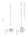
- Fig. 3 shows a sample configuration of a transmission device 300 pertaining to the present embodiment.
- An encoder 302A takes information (data) 301A and a frame configuration signal 313 as input (which includes the error-correction scheme, coding rate, block length, and other information used by the encoder 302A in error-correction coding of the data, such that the scheme designated by the frame configuration signal 313 is used. The error-correction scheme may be switched).
- the encoder 302A performs error-correction coding, such as convolutional encoding, LDPC encoding, turbo encoding or similar, and outputs encoded data 303A.
- An interleaver 304A takes the encoded data 303A and the frame configuration signal 313 as input, performs interleaving, i.e., rearranges the order thereof, and then outputs interleaved data 305A. (Depending on the frame configuration signal 313, the interleaving scheme may be switched.)
- a mapper 306A takes the interleaved data 305A and the frame configuration signal 313 as input and performs modulation, such as QPSK (Quadrature Phase Shift Keying), 16-QAM (16-Quadradature Amplitude Modulation), or 64-QAM (64-Quadradture Amplitude Modulation) thereon, then outputs a baseband signal 307A. (Depending on the frame configuration signal 313, the modulation scheme may be switched.)
- modulation such as QPSK (Quadrature Phase Shift Keying), 16-QAM (16-Quadradature Amplitude Modulation), or 64-QAM (64-Quadradture Amplitude Modulation)
- Figs. 19A and 19B illustrate an example of a QPSK modulation mapping scheme for a baseband signal made up of an in-phase component I and a quadrature component Q in the IQ plane.
- Fig. 19B illustrates an example of a QPSK modulation mapping scheme in the IQ plane differing from Fig. 19A in that the signal points of Fig. 19A have been rotated about the origin to obtain the signal points of Fig. 19B .
- Non-Patent Literature 9 and Non-Patent Literature 10 describe such a constellation rotation scheme.
- the Cyclic Q Delay described in Non-Patent Literature 9 and Non-Patent Literature 10 may also be adopted.
- An alternate example, distinct from Figs. 19A and 19B is shown in Figs. 20A and 20B , which illustrate a signal point arrangement for 16-QAM in the IQ plane.
- the example of Fig. 20A corresponds to Fig. 19A
- that of Fig. 20B corresponds to Fig. 19B .
- An encoder 302B takes information (data) 301B and the frame configuration signal 313 as input (which includes the error-correction scheme, coding rate, block length, and other information used by the encoder 302A in error-correction coding of the data, such that the scheme designated by the frame configuration signal 313 is used. The error-correction scheme may be switched).
- the encoder 302B performs error-correction coding, such as convolutional encoding, LDPC encoding, turbo encoding or similar, and outputs encoded data 303B.
- An interleaver 304B takes the encoded data 303B and the frame configuration signal 313 as input, performs interleaving, i.e., rearranges the order thereof, and outputs interleaved data 305B. (Depending on the frame configuration signal 313, the interleaving scheme may be switched.)
- a mapper 306B takes the interleaved data 305B and the frame configuration signal 313 as input and performs modulation, such as QPSK, 16-QAM, or 64-QAM thereon, then outputs a baseband signal 307B. (Depending on the frame configuration signal 313, the modulation scheme may be switched.)
- a signal processing scheme information generator 314 takes the frame configuration signal 313 as input and accordingly outputs signal processing scheme information 315.
- the signal processing scheme information 315 designates the fixed precoding matrix to be used, and includes information on the pattern of phase changes used for changing the phase.
- a weighting unit 308A takes baseband signal 307A, baseband signal 307B, and the signal processing scheme information 315 as input and, in accordance with the signal processing scheme information 315, performs weighting on the baseband signals 307A and 307B, then outputs a weighted signal 309A.
- the weighting scheme is described in detail, later.
- a wireless unit 310A takes weighted signal 309A as input and performs processing such as quadrature modulation, band limitation, frequency conversion, amplification, and so on, then outputs transmit signal 311A. Transmit signal 311A is then output as radio waves by an antenna 312A.
- a weighting unit 308B takes baseband signal 307A, baseband signal 307B, and the signal processing scheme information 315 as input and, in accordance with the signal processing scheme information 315, performs weighting on the baseband signals 307A and 307B, then outputs weighted signal 316B.
- Fig. 21 illustrates the configuration of the weighting units 308A and 308B.
- the area of Fig. 21 enclosed in the dashed line represents one of the weighting units.
- Baseband signal 307A is multiplied by w11 to obtain w11 ⁇ s1(t), and multiplied by w21 to obtain w21 ⁇ s1(t).
- baseband signal 307B is multiplied by w12 to obtain w12 ⁇ s2(t), and multiplied by w22 to obtain w22 ⁇ s2(t).
- z1(t) w11 ⁇ s1(t)+w12 ⁇ s2(t)
- z2(t) w21 ⁇ s1(t)+w22 ⁇ s22(t) are obtained.
- s1(t) and s2(t) are baseband signals modulated according to a modulation scheme such as BPSK (Binary Phase Shift Keying), QPSK, 8-PSK (8-Phase Shift Keying), 16-QAM, 32-QAM (32-Quadrature Amplitude Modulation), 64-QAM, 256-QAM 16-APSK (16-Amplitude Phase Shift Keying) and so on.
- BPSK Binary Phase Shift Keying
- QPSK Quadrature Shift Keying
- 8-PSK 8-Phase Shift Keying
- 16-QAM 32-QAM (32-Quadrature Amplitude Modulation)
- 64-QAM 64-QAM
- 256-QAM 16-APSK (16-Amplitude Phase Shift Keying
- Both weighting units perform weighting using a fixed precoding matrix.
- the precoding matrix uses, for example, the scheme of formula 36, and satisfies the conditions of formula 37 or formula 38, all found below. However, this is only an example.
- the precoding matrix is:
- ⁇ may be given by formula 37.
- ⁇ may be given by formula 38.
- the precoding matrix is not restricted to that of formula 36, but may also be as indicated by formula 39.
- a Ae j ⁇ 11
- b Be j ⁇ 12
- c Ce j ⁇ 21
- d De j ⁇ 22 .
- one of a, b, c, and d may be zero.
- the following configurations are possible: (1) a may be zero while b, c, and d are non-zero, (2) b may be zero while a, c, and d are non-zero, (3) c may be zero while a, b, and d are non-zero, or (4) d may be zero while a, b, and c are non-zero.
- the precoding matrix may also be set, changed, and fixed for use.
- a phase changer 317B takes weighted signal 316B and the signal processing scheme information 315 as input, then regularly changes the phase of the signal 316B for output.
- This regular change is a change of phase performed according to a predetermined phase changing pattern having a predetermined period (cycle) (e.g., every n symbols (n being an integer, n ⁇ 1) or at a predetermined interval).
- a predetermined period e.g., every n symbols (n being an integer, n ⁇ 1) or at a predetermined interval.
- Wireless unit 310B takes post-phase-change signal 309B as input and performs processing such as quadrature modulation, band limitation, frequency conversion, amplification, and so on, then outputs transmit signal 311B. Transmit signal 311B is then output as radio waves by an antenna 312B.
- Fig. 4 illustrates a sample configuration of a transmission device 400 that differs from that of Fig. 3 .
- the points of difference of Fig. 4 from Fig. 3 are described next.
- An encoder 402 takes information (data) 401 and the frame configuration signal 313 as input, and, in accordance with the frame configuration signal 313, performs error-correction coding and outputs encoded data 402.
- a distributor 404 takes the encoded data 403 as input, performs distribution thereof, and outputs data 405A and data 405B.
- Fig. 4 illustrates only one encoder, the number of encoders is not limited as such.
- the present invention may also be realized using m encoders (m being an integer, m ⁇ 1) such that the distributor divides the encoded data created by each encoder into two groups for distribution.
- Fig. 5 illustrates an example of a frame configuration in the time domain for a transmission device according to the present embodiment.
- Symbol 500_1 is for notifying the reception device of the transmission scheme.
- symbol 500_1 conveys information such as the error-correction scheme used for transmitting data symbols, the coding rate thereof, and the modulation scheme used for transmitting data symbols.
- Symbol 501_1 is for estimating channel fluctuations for modulated signal z1(t) (where t is time) transmitted by the transmission device.
- Symbol 502_1 is a data symbol transmitted by modulated signal z1(t) as symbol number u (in the time domain).
- Symbol 503_1 is a data symbol transmitted by modulated signal z1(t) as symbol number u+1.
- Symbol 501_2 is for estimating channel fluctuations for modulated signal z2(t) (where t is time) transmitted by the transmission device.
- Symbol 502_2 is a data symbol transmitted by modulated signal z2(t) as symbol number u (in the time domain).
- Symbol 503_2 is a data symbol transmitted by modulated signal z1(t) as symbol number u+1.
- the symbols of z1(t) and of z2(t) having the same time are transmitted from the transmit antenna using the same (shared/common) frequency.
- the following describes the relationships between the modulated signals z1(t) and z2(t) transmitted by the transmission device and the received signals r1(t) and r2(t) received by the reception device.
- 504#1 and 504#2 indicate transmit antennas of the transmission device, while 505#1 and 505#2 indicate receive antennas of the reception device.
- the transmission device transmits modulated signal z1(t) from transmit antenna 504#1 and transmits modulated signal z2(t) from transmit antenna 504#2.
- the modulated signals z1(t) and z2(t) are assumed to occupy the same (shared/common) frequency (band).
- the channel fluctuations in the transmit antennas of the transmission device and the antennas of the reception device are h 11 (t), h 12 (t), h 21 (t), and h 22 (t), respectively.
- receive antenna 505#1 of the reception device receives received signal r1(t) and that receive antenna 505#2 of the reception device receives received signal r2(t)
- Fig. 6 pertains to the weighting scheme (precoding scheme) and the phase changing scheme of the present embodiment.
- a weighting unit 600 is a combined version of the weighting units 308A and 308B from Fig. 3 .
- stream s1(t) and stream s2(t) correspond to the baseband signals 307A and 307B of Fig. 3 . That is, the streams s1(t) and s2(t) are baseband signals made up of an in-phase component I and a quadrature component Q conforming to mapping by a modulation scheme such as QPSK, 16-QAM, and 64-QAM.
- a modulation scheme such as QPSK, 16-QAM, and 64-QAM.
- stream s1(t) is represented as s1(u) at symbol number u, as s1(u+1) at symbol number u+1, and so forfh.
- stream s2(t) is represented as s2(u) at symbol number u, as s2(u+1) at symbol number u+1, and so forth.
- the weighting unit 600 takes the baseband signals 307A (s1(t)) and 307B (s2(t)) as well as the signal processing scheme information 315 from Fig. 3 as input, performs weighting in accordance with the signal processing scheme information 315, and outputs the weighted signals 309A (z1(t)) and 316B(z2'(t)) from Fig. 3 .
- the phase changer 317B changes the phase of weighted signal 316B(z2'(t)) and outputs post-phase-change signal 309B(z2(t)).
- y(t) is a phase changing formula following a predetermined scheme. For example, given a period (cycle) of four and time u, the phase changing formula is expressible as formula 43, below.
- phase changing formula for time u+1 may be, for example, as given by formula 44.
- phase changing formula for time u+k is expressible as formula 45.
- the regular change of phase is not restricted to a period (cycle) of four.
- Improved reception capabilities (the error-correction capabilities, to be exact) may potentially be promoted in the reception device by increasing the period (cycle) number (this does not mean that a greater period (cycle) is better, though avoiding small numbers such as two is likely ideal).
- formula 43 through formula 45 represent a configuration in which a change in phase is carried out through rotation by consecutive predetermined phases (in the above formula, every ⁇ /2), the change in phase need not be rotation by a constant amount, but may also be random.
- the phase in accordance with the predetermined period (cycle) of y(t), the phase may be changed through sequential multiplication as shown in formula 46 and formula 47.
- the key point of regular phase changing is that the phase of the modulated signal is regularly changed.
- the degree of phase change is preferably as even as possible, such as from - ⁇ radians to ⁇ radians. However, given that this describes a distribution, random changes are also possible.
- the weighting unit 600 of Fig. 6 performs precoding using fixed, predetermined precoding weights, and the phase changer 317B changes the phase of the signal input thereto while regularly varying the phase changing degree.
- the reception quality is likely to improve tremendously.
- the phase and amplitude components of the direct wave may greatly differ from the specialized precoding matrix, upon reception.
- the LOS environment has certain rules.
- data reception quality is tremendously improved through a regular change applied to a transmit signal that obeys those rules.
- the present invention offers a signal processing scheme for improvements in the LOS environment.
- Fig. 7 illustrates a sample configuration of a reception device 700 pertaining to the present embodiment.
- Wireless unit 703_X receives, as input, received signal 702_X received by antenna 701_X, performs processing such as frequency conversion, quadrature demodulation, and the like, and outputs baseband signal 704_X.
- Channel fluctuation estimator 705_1 for modulated signal z1 transmitted by the transmission device takes baseband signal 704_X as input, extracts reference symbol 501_1 for channel estimation from Fig. 5 , estimates the value of h 11 from formula 40, and outputs channel estimation signal 706_1.
- Channel fluctuation estimator 705_2 for modulated signal z2 transmitted by the transmission device takes baseband signal 704_X as input, extracts reference symbol 501_2 for channel estimation from Fig. 5 , estimates the value of h 12 from formula 40, and outputs channel estimation signal 706_2.
- Wireless unit 703_Y receives, as input, received signal 702_Y received by antenna 701_X, performs processing such as frequency conversion, quadrature demodulation, and the like, and outputs baseband signal 704_Y.
- Channel fluctuation estimator 707_1 for modulated signal z1 transmitted by the transmission device takes baseband signal 704_Y as input, extracts reference symbol 501_1 for channel estimation from Fig. 5 , estimates the value of h 21 from formula 40, and outputs channel estimation signal 708_1.
- Channel fluctuation estimator 707_2 for modulated signal z2 transmitted by the transmission device takes baseband signal 704_Y as input, extracts reference symbol 501_2 for channel estimation from Fig. 5 , estimates the value of h 22 from formula 40, and outputs channel estimation signal 708_2.
- a control information decoder 709 receives baseband signal 704_X and baseband signal 704_Y as input, detects symbol 500_1 that indicates the transmission scheme from Fig. 5 , and outputs a transmission scheme information signal 710 for the transmission device.
- a signal processor 711 takes the baseband signals 704_X and 704_Y, the channel estimation signals 706_1, 706_2, 708_1, and 708_2, and the transmission scheme information signal 710 as input, performs detection and decoding, and then outputs received data 712_1 and 712_2.
- Fig. 8 illustrates a sample configuration of the signal processor 711 pertaining to the present embodiment.
- the signal processor 711 is primarily made up of an inner MIMO detector, soft-in/soft-out decoders, and a coefficient generator.
- Non-Patent Literature 2 and Non-Patent Literature 3 describe a scheme of iterative decoding using this structure.
- the MIMO system described in Non-Patent Literature 2 and Non-Patent Literature 3 is a spatial multiplexing MIMO system, while the present embodiment differs from Non-Patent Literature 2 and Non-Patent Literature 3 in describing a MIMO system that regularly changes the phase over time while using the same precoding matrix.
- the precoding weight matrix from Fig. 6 be F (here, a fixed precoding matrix remaining unchanged for a given received signal) and letting the phase changing formula used by the phase changer from Fig.
- the reception device may use the decoding schemes of Non-Patent Literature 2 and 3 on R(t) by computing H(t) ⁇ Y(t) ⁇ F.
- the coefficient generator 819 from Fig. 8 takes a transmission scheme information signal 818 (corresponding to 710 from Fig. 7 ) indicated by the transmission device (information for specifying the fixed precoding matrix in use and the phase changing pattern used when the phase is changed) and outputs a signal processing scheme information signal 820.
- the inner MIMO detector 803 takes the signal processing scheme information signal as input and performs iterative detection and decoding using the signal and the relationship thereof to formula 48. The operations thereof are described below.
- the processor illustrated in Fig. 8 uses a processing scheme, as illustrated by Fig. 10 , to perform iterative decoding (iterative detection).
- detection of one codeword (or one frame) of modulated signal (stream) s1 and of one codeword (or one frame) of modulated signal (stream) s2 is performed.
- the soft-in/soft-out decoder obtains the log-likelihood ratio of each bit of the codeword (or frame) of modulated signal (stream) s1 and of the codeword (or frame) of modulated signal (stream) s2.
- the log-likelihood ratio is used to perform a second round of detection and decoding. These operations are performed multiple times (these operations are hereinafter referred to as iterative decoding (iterative detection)).
- the following explanations center on the creation scheme of the log-likelihood ratio of a symbol at a specific time within one frame.
- a memory 815 takes baseband signal 801X (corresponding to baseband signal 704_X from Fig. 7 ), channel estimation signal group 802X (corresponding to channel estimation signals 706_1 and 706_2 from Fig. 7 ), baseband signal 801Y (corresponding to baseband signal 704_Y from Fig. 7 ), and channel estimation signal group 802Y (corresponding to channel estimation signals 708_1 and 708_2 from Fig. 7 ) as input, executes (computes) H(t) ⁇ Y(t) ⁇ F from formula 48 in order to perform iterative decoding (iterative detection) and stores the resulting matrix as a transformed channel signal group.
- the memory 815 then outputs the above-described signals as needed, specifically as baseband signal 816X, transformed channel estimation signal group 817X, baseband signal 816Y, and transformed channel estimation signal group 817Y.
- the inner MIMO detector 803 takes baseband signal 801X, channel estimation signal group 802X, baseband signal 801Y, and channel estimation signal group 802Y as input.
- the modulation scheme for modulated signal (stream) s1 and modulated signal (stream) s2 is taken to be 16-QAM.
- the inner MIMO detector 803 first computes H(t) ⁇ Y(t) ⁇ F from the channel estimation signal groups 802X and 802Y, thus calculating a candidate signal point corresponding to baseband signal 801X.
- Fig. 11 represents such a calculation.
- each black dot is a candidate signal point in the IQ plane.
- the modulation scheme is 16-QAM, 256 candidate signal points exist. (However, Fig.
- 11 is only a representation and does not indicate all 256 candidate signal points.) Letting the four bits transmitted in modulated signal s1 be b0, b1, b2, and b3 and the four bits transmitted in modulated signal s2 be b4, b5, b6, and b7, candidate signal points corresponding to (b0, b1, b2, b3, b4, b5, b6, b7) are found in Fig. 11 . The Euclidean squared distance between each candidate signal point and each received signal point 1101 (corresponding to baseband signal 801X) is then computed. The Euclidian squared distance between each point is divided by the noise variance ⁇ 2 .
- E x (b0, b1, b2, b3, b4, b5, b6, b7) is calculated. That is, E x is the Euclidian squared distance between a candidate signal point (corresponding to (b0, b1, b2, b3, b4, b5, b6, b7) and a received signal point, divided by the noise variance.
- each of the baseband signals and the modulated signals s1 and s2 is a complex signal.
- the inner MIMO detector 803 computes H(t)xY(t)xF from the channel estimation signal groups 802X and 802Y, calculates candidate signal points corresponding to baseband signal 801Y, computes the Euclidean squared distance between each of the candidate signal points and the received signal points (corresponding to baseband signal 801Y), and divides the Euclidean squared distance by the noise variance ⁇ 2 . Accordingly, E Y (b0, b1, b2, b3, b4, b5, b6, b7) is calculated. That is, E Y is the Euclidian squared distance between a candidate signal point corresponding to (b0, b1, b2, b3, b4, b5, b6, b7) and a received signal point, divided by the noise variance.
- E X (b0, b1, b2, b3, b4, b5, b6, b7)+E Y (b0, b1, b2, b3, b4, b5, b6, b7) E(b0, b1, b2, b3, b4, b5, b6, b7) is computed.
- the inner MIMO detector 803 outputs E(b0, b1, b2, b3, b4, b5, b6, b7) as a signal 804.
- Log-likelihood calculator 805A takes the signal 804 as input, calculates the log-likelihood of bits b0, b1, b2, and b3, and outputs log-likelihood signal 806A. Note that this log-likelihood calculation produces the log-likelihood of a bit being 1 and the log-likelihood of a bit being 0.
- the calculation scheme is as shown in formula 28, formula 29, and formula 30, and the details are given by Non-Patent Literature 2 and 3.
- log-likelihood calculator 805A takes the signal 804 as input, calculates the log-likelihood of bits b0, b1, b2, and b3, and outputs log-likelihood signal 806B.
- a deinterleaver (807A) takes log-likelihood signal 806A as input, performs deinterleaving corresponding to that of the interleaver (the interleaver (304A) from Fig. 3 ), and outputs deinterleaved log-likelihood signal 808A.
- a deinterleaver (807B) takes log-likelihood signal 806B as input, performs deinterleaving corresponding to that of the interleaver (the interleaver (304B) from Fig. 3 ), and outputs deinterleaved log-likelihood signal 808B.
- Log-likelihood ratio calculator 809A takes deinterleaved log-likelihood signal 808A as input, calculates the log-likelihood ratio of the bits encoded by encoder 302A from Fig. 3 , and outputs log-livelihood ratio signal 810A.
- log-likelihood ratio calculator 809B takes deinterleaved log-likelihood signal 808B as input, calculates the log-likelihood ratio of the bits encoded by encoder 302B from Fig. 3 , and outputs log-likelihood ratio signal 810B.
- Soft-in/soft-out decoder 811A takes log-likelihood ratio signal 810A as input, performs decoding, and outputs decoded log-likelihood ratio 812A.
- soft-in/soft-out decoder 811B takes log-likelihood ratio signal 810B as input, performs decoding, and outputs decoded log-likelihood ratio 812B.
- the interleaver (813A) takes the k-1th decoded log-likelihood ratio 812A decoded by the soft-in/soft-out decoder as input, performs interleaving, and outputs interleaved log-likelihood ratio 814A.
- the interleaving pattern used by the interleaver (813A) is identical to that of the interleaver (304A) from Fig. 3 .
- Another interleaver (813B) takes the k-1th decoded log-likelihood ratio 812B decoded by the soft-in/soft-out decoder as input, performs interleaving, and outputs interleaved log-likelihood ratio 814B.
- the interleaving pattern used by the other interleaver (813B) is identical to that of another interleaver (304B) from Fig. 3 .
- the inner MIMO detector 803 takes baseband signal 816X, transformed channel estimation signal group 817X, baseband signal 816Y, transformed channel estimation signal group 817Y, interleaved log-likelihood ratio 814A, and interleaved log-likelihood ratio 814B as input.
- baseband signal 816X, transformed channel estimation signal group 817X, baseband signal 816Y, and transformed channel estimation signal group 817Y are used instead of baseband signal 801X, channel estimation signal group 802X baseband signal 801Y, and channel estimation signal group 802Y because the latter cause delays due to the iterative decoding.
- the iterative decoding operations of the inner MIMO detector 803 differ from the initial detection operations thereof in that the interleaved log-likelihood ratios 814A and 814B are used in signal processing for the former.
- the inner MIMO detector 803 first calculates E(b0, b1, b2, b3, b4, b5, b6, b7) in the same manner as for initial detection.
- the coefficients corresponding to formula 11 and formula 32 are computed from the interleaved log-likelihood ratios 814A and 814B.
- E(b0, b1, b2, b3, b4, b5, b6, b7) is corrected using the coefficients so calculated to obtain E'(b0, b2, b3, b4, b5, b6, b7), which is output as the signal 804.
- Log-likelihood calculator 805A takes the signal 804 as input, calculates the log-likelihood of bits b0, b2, and b3, and outputs the log-likelihood signal 806A. Note that this log-likelihood calculation produces the log-likelihood of a bit being 1 and the log-likelihood of a bit being 0.
- the calculation scheme is as shown in formula 31 through formula 35, and the details are given by Non-Patent Literature 2 and 3.
- log-likelihood calculator 805B takes the signal 804 as input, calculates the log-likelihood of bits b4, b5, b6, and b7, and outputs the log-likelihood signal 806A. Operations performed by the deinterleaver onwards are similar to those performed for initial detection.
- Fig. 8 illustrates the configuration of the signal processor when performing iterative detection
- this structure is not absolutely necessary as good reception improvements are obtainable by iterative detection alone.
- the configuration need not include the interleavers 813A and 813B. In such a case, the inner MIMO detector 803 does not perform iterative detection.
- QR decomposition may also be used to perform initial detection and iterative detection.
- MMSE Minimum Mean-Square Error
- ZF Zero-Forcing linear operations
- Fig. 9 illustrates the configuration of a signal processor, unlike that of Fig. 8 , that serves as the signal processor for modulated signals transmitted by the transmission device from Fig. 4 .
- the point of difference from Fig. 8 is the number of soft-in/soft-out decoders.
- a soft-in/soft-out decoder 901 takes the log-likelihood ratio signals 810A and 810B as input, performs decoding, and outputs a decoded log-likelihood ratio 902.
- a distributor 903 takes the decoded log-likelihood ratio 902 as input for distribution. Otherwise, the operations are identical to those explained for Fig. 8 .
- a transmission device when a transmission device according to the present embodiment using a MIMO system transmits a plurality of modulated signals from a plurality of antennas, changing the phase over time while multiplying by the precoding matrix so as to regularly change the phase results in improvements to data reception quality for a reception device in a LOS environment where direct waves are dominant, in contrast to a conventional spatial multiplexing MIMO system.
- the number of antennas is limited and explanations are given accordingly.
- the Embodiment may also be applied to a greater number of antennas. In other words, the number of antennas in the reception device does not affect the operations or advantageous effects of the present embodiment.
- LDPC codes are described as a particular example, the present embodiment is not limited in this manner.
- the decoding scheme is not limited to the sum-product decoding example given for the soft-in/soft-out decoder.
- Other soft-in/soft-out decoding schemes such as the BCJR algorithm, SOVA, and the Max-Log-Map algorithm may also be used. Details are provided in Non-Patent Literature 6.
- the present embodiment is described using a single-carrier scheme, no limitation is intended in this regard.
- the present embodiment is also applicable to multi-carrier transmission.
- the present embodiment may also be realized using, for example, spread-spectrum communications, OFDM (Orthogonal Frequency-Division Multiplexing), SC-FDMA (Single Carrier Frequency-Division Multiple Access), SC-OFDM (Single Carrier Orthogonal Frequency-Division Multiplexing), wavelet OFDM as described in Non-Patent Literature 7, and so on.
- symbols other than data symbols such as pilot symbols (preamble, unique word, etc) or symbols transmitting control information, may be arranged within the frame in any manner.
- Fig. 12 illustrates the configuration of a transmission device using OFDM.
- components operating in the manner described for Fig. 3 use identical reference numbers.
- OFDM-related processor 1201A takes weighted signal 309A as input, performs OFDM-related processing thereon, and outputs transmit signal 1202A.
- OFDM-related processor 1201B takes post-phase-change signal 309B as input, performs OFDM-related processing thereon, and outputs transmit signal 1202A
- Fig. 13 illustrates a sample configuration of the OFDM-related processors 1201A and 1201B and onward from Fig. 12 .
- Components 1301A through 1310A belong between 1201A and 312A from Fig. 12
- components 1301B through 1310B belong between 1201B and 312B.
- Serial-to-parallel converter 1302A performs serial-to-parallel conversion on weighted signal 1301A (corresponding to weighted signal 309A from Fig. 12 ) and outputs parallel signal 1303A.
- Reorderer 1304A takes parallel signal 1303A as input, performs reordering thereof, and outputs reordered signal 1305A. Reordering is described in detail later.
- IFFT (Inverse Fast Fourier Transform) unit 1306A takes reordered signal 1305A as input, applies an IFFT thereto, and outputs post-IFFT signal 1307A.
- Wireless unit 1308A takes post-IFFT signal 1307A as input, performs processing such as frequency conversion and amplification, thereon, and outputs modulated signal 1309A. Modulated signal 1309A is then output as radio waves by antenna 1310A.
- Serial-to-parallel converter 1302B performs serial-to-parallel conversion on weighted signal 1301B (corresponding to post-phase-change signal 309B from Fig. 12 ) and outputs parallel signal 1303B.
- Reorderer 1304B takes parallel signal 1303B as input, performs reordering thereof, and outputs reordered signal 1305B. Reordering is described in detail later.
- IFFT unit 1306B takes reordered signal 1305B as input, applies an IFFT thereto, and outputs post-IFFT signal 1307B.
- Wireless unit 1308B takes post-IFFT signal 1307B as input, performs processing such as frequency conversion and amplification thereon, and outputs modulated signal 1309B. Modulated signal 1309B is then output as radio waves by antenna 1310A.
- the transmission device from Fig. 3 does not use a multi-carrier transmission scheme.
- the change of phase is performed to achieve a period (cycle) of four and the post-phase-change symbols are arranged with respect to the time domain.
- Fig. 12 when multi-carrier transmission, such as OFDM, is used, then, naturally, precoded post-phase-change symbols may be arranged with respect to the time domain as in Fig. 3 , and this applies to each (sub-)carrier.
- the arrangement may also be in the frequency domain, or in both the frequency domain and the time domain. The following describes these arrangements.
- Figs. 14A and 14B indicate frequency on the horizontal axes and time on the vertical axes thereof, and illustrate an example of a symbol reordering scheme used by the reorderers 1304A and 1304B from Fig. 13 .
- the frequency axes are made up of (sub-)carriers 0 through 9.
- the modulated signals z1 and z2 share common time (timing) and use a common frequency band.
- Fig. 14A illustrates a reordering scheme for the symbols of modulated signal z1
- Fig. 14B illustrates a reordering scheme for the symbols of modulated signal z2.
- the assigned ordering is #0, #1, #2, #3, and so on.
- #0, #1, #2, and #3 are equivalent to one period (cycle).
- #4n, #4n+1, #4n+2, and #4n+3 are also equivalent to one period (cycle).
- symbols #0, #1, #2, #3, and so on are arranged in order, beginning at carrier 0. Symbols #0 through #9 are given time $1, followed by symbols #10 through #19 which are given time #2, and so on in a regular arrangement. Note that the modulated signals z1 and z2 are complex signals.
- the assigned ordering is #0, #1, #2, #3, and so on.
- a different change of phase is applied to each of #0, #1, #2, and #3, which are equivalent to one period (cycle).
- a different change of phase is applied to each of #4n, #4n+1, #4n+2, and #4n+3 (n being a non-zero positive integer), which are also equivalent to one period (cycle)
- symbols #0, #1, #2, #3, and so on are arranged in order, beginning at carrier 0. Symbols #0 through #9 are given time $1, followed by symbols #10 through #19 which are given time #2, and so on in a regular arrangements.
- the symbol group 1402 shown in Fig. 14B corresponds to one period (cycle) of symbols when the phase changing scheme of Fig. 6 is used.
- Symbol #0 is the symbol obtained by using the phase at time u in Fig. 6
- symbol #1 is the symbol obtained by using the phase at time u+1 in Fig. 6
- symbol #2 is the symbol obtained by using the phase at time u+2 in Fig. 6
- symbol #3 is the symbol obtained by using the phase at time u+3 in Fig. 6 .
- symbol #x is the symbol obtained by using the phase at time u in Fig.
- symbol #x is the symbol obtained by using the phase at time u+1 in Fig. 6 when x mod 4 equals 1
- symbol #x is the symbol obtained by using the phase at time u+2 in Fig. 6 when x mod 4 equals 2
- symbol #x is the symbol obtained by using the phase at time u+3 in Fig. 6 when x mod 4 equals 3.
- modulated signal z1 shown in Fig. 14A has not undergone a change of phase.
- symbols may be arranged with respect to the frequency domain.
- the symbol arrangement scheme is not limited to those illustrated by Figs. 14A and 14B . Further examples are shown in Figs. 15A, 15B , 16A, and 16B .
- Figs. 15A and 15B indicate frequency on the horizontal axes and time on the vertical axes thereof, and illustrate an example of a symbol reordering scheme used by the reorderers 1304A and 1304B from Fig. 13 that differs from that of Figs. 14A and 14B .
- Fig. 15A illustrates a reordering scheme for the symbols of modulated signal z1
- Fig. 15B illustrates a reordering scheme for the symbols of modulated signal z2.
- Figs. 15A and 15B differ from Figs. 14A and 14B in that different reordering schemes are applied to the symbols of modulated signal z1 and to the symbols of modulated signal z2.
- Fig. 15A and 15B indicate frequency on the horizontal axes and time on the vertical axes thereof, and illustrate an example of a symbol reordering scheme used by the reorderers 1304A and 1304B from Fig. 13 that differs from that of Figs. 14A and
- symbol group 1502 shown in Fig. 15B corresponds to one period (cycle) of symbols when the phase changing scheme of Fig. 6 is used
- Figs. 16A and 16B indicate frequency on the horizontal axes and time on the vertical axes thereof, and illustrate an example of a symbol reordering scheme used by the reorderers 1304A and 1304B from Fig. 13 that differs from that of Figs. 14A and 14B .
- Fig. 16A illustrates a reordering scheme for the symbols of modulated signal z 1
- Fig. 16B illustrates a reordering scheme for the symbols of modulated signal z2.
- Figs. 16A and 16B differ from Figs. 14A and 14B in that, while Figs. 14A and 14B showed symbols arranged at sequential carriers, Figs. 16A and 16B do not arrange the symbols at sequential carriers.
- different reordering schemes may be applied to the symbols of modulated signal z1 and to the symbols of modulated signal z2 as in Figs. 15A and 15B .
- Figs. 17A and 17B indicate frequency on the horizontal axes and time on the vertical axes thereof, and illustrate an example of a symbol reordering scheme used by the reordered 1304A and 1304B from Fig. 13 that differs from those of Figs. 14A through 16B .
- Fig. 17A illustrates a reordering scheme for the symbols of modulated signal z 1
- Fig. 17B illustrates a reordering scheme for the symbols of modulated signal z2. While Figs. 14A through 16B show symbols arranged with respect to the frequency axis, Figs. 17A and 17B use the frequency and time axes together in a single arrangements.
- the symbol group 1702 is equivalent to one period (cycle) of symbols when the phase changing scheme is used (i.e., to eight symbols) such that symbol #0 is the symbol obtained by using the phase at time u, symbol #1 is the symbol obtained by using the phase at time u+1, symbol #2 is the symbol obtained by using the phase at time u+2, symbol #3 is the symbol obtained by using the phase at time u+3, symbol #4 is the symbol obtained by using the phase at time u+4, symbol #5 is the symbol obtained by using the phase at time u+5, symbol #6 is the symbol obtained by using the phase at time u+6, and symbol #7 is the symbol obtained by using the phase at time u+7.
- symbol #x is the symbol obtained by using the phase at time u when x mod 8 equals 0
- symbol #x is the symbol obtained by using the phase at time u+1 when x mod 8 equals 1
- symbol #x is the symbol obtained by using the phase at time u+2 when x mod 8 equals 2
- symbol #x is the symbol obtained by using the phase at time u+3 when x mod 8 equals 3
- symbol #x is the symbol obtained by using the phase at time u+4 when x mod 8 equals 4
- symbol #x is the symbol obtained by using the phase at time u+5 when x mod 8 equals 5
- symbol #x is the symbol obtained by using the phase at time u+6 when x mod 8 equals 6
- symbol #x is the symbol obtained by using the phase at time u+7 when x mod 8 equals 7.
- n slots (carriers) in the frequency domain and m slots in the time domain should be used to arrange the symbols of each period (cycle), such that m > n.
- the phase changing period (cycle) should preferably reduce direct wave fluctuations.
- m should be greater than n.
- using the time and frequency domains together for reordering is preferable to using either of the frequency domain or the time domain alone due to the strong probability of the direct waves becoming regular. As a result, the effects of the present invention are more easily obtained.
- reordering in the frequency domain may lead to diversity gain due the fact that frequency-domain fluctuations are abrupt. As such, using the frequency and time domains together for reordering is not always ideal.
- Figs. 18A and 18B indicate frequency on the horizontal axes and time on the vertical axes thereof, and illustrate an example of a symbol reordering scheme used by the reorderers 1304A and 1304B from Fig. 13 that differs from that of Figs. 17A and 14B .
- Fig. 18A illustrates a reordering scheme for the symbols of modulated signal z1
- Fig. 18B illustrates a reordering scheme for the symbols of modulated signal z2.
- Figs. 18A and 18B illustrate the use of the time and frequency domains, together.
- Figs. 18A and 18B illustrate the use of the time and frequency domains, together.
- Figs. 18A and 18B illustrate the use of the time and frequency domains, together.
- Figs. 18A and 18B illustrate the use of the time and frequency domains, together.
- Figs. 18A and 18B illustrate the use of the time and frequency domains, together.
- Figs. 18A and 18B prioritize the time domain and use the frequency domain for secondary symbol arrangement.
- symbol group 1802 corresponds to one period (cycle) of symbols when the phase changing scheme is used.
- the reordering scheme applied to the symbols of modulated signal z1 and the symbols of modulated signal z2 may be identical or may differ as in Figs. 15A and 15B . Both approaches allow good reception quality to be obtained. Also, in Figs. 17A, 17B , 18A, and 18B , the symbols may be arranged non-sequentially as in Figs. 16A and 16B . Both approaches allow good reception quality to be obtained.
- Fig. 22 indicates frequency on the horizontal axis and time on the vertical axis thereof, and illustrates an example of a symbol reordering scheme used by the reorderers 1304A and 1304B from Fig. 13 that differs from the above.
- Fig. 22 illustrates a regular phase changing scheme using four slots, similar to time u through u+3 from Fig. 6 .
- the frequency-domain symbol group 2210 in Fig. 22 indicates four symbols to which the change of phase is applied at time u through u+3 from Fig. 6 .
- symbol #0 is obtained through a change of phase at time u
- symbol #1 is obtained through a change of phase at time u+1
- symbol #2 is obtained through a change of phase at time u+2
- symbol #3 is obtained through a change of phase at time u+3.
- symbol #4 is obtained through a change of phase at time u
- symbol #5 is obtained through a change of phase at time u+1
- symbol #6 is obtained through a change of phase at time u+2
- symbol #7 is obtained through a change of phase at time u+3.
- symbol #0 is obtained through a change of phase at time u
- symbol #9 is obtained through a change of phase at time u+1
- symbol #18 is obtained through a change of phase at time u+2
- symbol #27 is obtained through a change of phase at time u+3.
- symbol #28 is obtained through a change of phase at time u
- symbol #1 is obtained through a change of phase at time u+1
- symbol #10 is obtained through a change of phase at time u+2
- symbol #19 is obtained through a change of phase at time u+3.
- symbol #20 is obtained through a change of phase at time u
- symbol #29 is obtained through a change of phase at time u+1
- symbol #2 is obtained through a change of phase at time u+2
- symbol #11 is obtained through a change of phase at time u+3.
- symbol #12 is obtained through a change of phase at time u
- symbol #21 is obtained through a change of phase at time u+1
- symbol #30 is obtained through a change of phase at time u+2
- symbol #3 is obtained through a change of phase at time u+3.
- Fig. 22 The characteristic feature of Fig. 22 is seen in that, taking symbol #11 as an example, the two neighbouring symbols thereof having the same time in the frequency domain (#10 and #12) are both symbols changed using a different phase than symbol #11, and the two neighbouring symbols thereof having the same carrier in the time domain (#2 and #20) are both symbols changed using a different phase than symbol #11.
- symbol #11 the two neighbouring symbols thereof having the same time in the frequency domain
- #2 and #20 are both symbols changed using a different phase than symbol #11
- phase changing is effectively carried out. This is highly likely to improve date reception quality as influence from regularizing direct waves is less prone to reception.
- Embodiment 1 phase changing is applied to a weighted (precoded with a fixed precoding matrix) signal z(t).
- the following Embodiments describe various phase changing schemes by which the effects of Embodiment 1 may be obtained.
- phase changer 317B is configured to perform a change of phase on only one of the signals output by the weighting unit 600.
- phase changing may also be applied before precoding is performed by the weighting unit 600.
- the transmission device may also feature the weighting unit 600 before the phase changer 317B, as shown in Fig. 25 .
- phase changing may be performed on both modulated signals s1(t) and s2(t).
- the transmission device is configured so as to include a phase changer taking both signals output by the weighting unit 600, as shown in Fig. 26 .
- phase changer 317A performs regular a regular change of phase on the signal input thereto, and as such changes the phase of signal z1'(t) precoded by the weighting unit. Post-phase-change signal z1(t) is then output to a transmitter.
- phase changing rate applied by the phase changers 317A and 317B varies simultaneously in order to perform the phase changing shown in Fig. 26 .
- the regular phase changing period (cycle) may be the same for both phase changers 317A and 317B, or may vary for each.
- a change of phase may be performed before precoding is performed by the weighting unit.
- the transmission device should be configured as illustrated in Fig. 27 .
- each of the transmit signals is, for example, control information that includes information about the phase changing pattern.
- the reception device knows the phase changing scheme by which the transmission device regularly varies the change, i.e., the phase changing pattern, and is thus able to demodulate (decode) the signals correctly.
- Fig. 28 differs from Fig. 6 in the inclusion of phase change ON/OFF information 2800 and in that the change of phase is performed on only one of z1'(t) and z2'(t) (i.e., performed on one of z1'(t) and z2'(t), which have identical time or a common frequency). Accordingly, in order to perform the change of phase on one of z1'(t) and z2'(t), the phase changers 317A and 317B shown in Fig. 28 may each be ON, and performing the change of phase, or OFF, and not performing the change of phase.
- the phase change ON/OFF information 2800 is control information therefor.
- the phase change ON/OFF information 2800 is output by the signal processing scheme information generator 314 shown in Fig. 3 .
- the two intervals form a phase changing period (cycle). While the above explanation describes the interval where the change of phase is performed on z 1'(t) only and the interval where the change of phase is performed on z2'(t) only as being equal, no limitation is intended in this manner. The two intervals may also differ. In addition, while the above explanation describes performing a change of phase having a period (cycle) of four on z1'(t) only and then performing a change of phase having a period (cycle) of four on z2'(t) only, no limitation is intended in this manner.
- the changes of phase may be performed on z1'(t) and on z2'(t) in any order (e.g., the change of phase may alternate between being performed on z 1'(t) and on z2'(t), or may be performed in random order).
- the two intervals form a phase changing period (cycle).
- the two intervals may also differ.
- the above explanation describes performing the change of phase having a period (cycle) of four on s1(t) only and then performing the change of phase having a period (cycle) of four on s2(t) only, no limitation is intended in this manner.
- the changes of phase may be performed on s1(t) and on s2(t) in any order (e.g., may alternate between being performed on s1(t) and on s2(t), or may be performed in random order).
- the reception conditions under which the reception device receives each transmit signal z1(t) and z2(t) are equalized.
- the ability of the error corrected codes to correct errors may be improved, thus ameliorating received signal quality in the LOS environment.
- Embodiment 2 as described above is able to produce the same results as the previously described Embodiment 1.
- the present embodiment used a single-carrier scheme, i.e., time domain phase changing, as an example, no limitation is intended in this regard. The same effects are also achievable using multi-carrier transmission. Accordingly, the present embodiment may also be realized using, for example, spread-spectrum communications, OFDM, SC-FDMA (Single Carrier Frequency-Division Multiple Access), SC-OFDM, wavelet OFDM as described in Non-Patent Literature 7, and so on. As previously described, while the present embodiment explains the change of phase as changing the phase with respect to the time domain t, the phase may alternatively be changed with respect to the frequency domain as described in Embodiment 1.
- phase changing scheme in the time domain t described in the present embodiment leads to a change of phase applicable to the frequency domain.
- the phase changing scheme of the present embodiment is also applicable to changing the phase with respect both the time domain and the frequency domain.
- Figs. 6 , 25 , 26 , and 27 illustrate changes of phase in the time domain
- replacing time t with carrier f in each of Figs. 6 , 25 , 26 , and 27 corresponds to a change of phase in the frequency domain.
- replacing (t) with (t, f) where t is time and f is frequency corresponds to performing the change of phase on time-frequency blocks.
- symbols other than data symbols such as pilot symbols (preamble, unique word, etc) or symbols transmitting control information, may be arranged within the frame in any manner.
- Embodiments 1 and 2 discuss regular changes of phase.
- Embodiment 3 describes a scheme of allowing the reception device to obtain good received signal quality for data, regardless of the reception device arrangement, by considering the location of the reception device with respect to the transmission device.
- Embodiment 3 concerns the symbol arrangement within signals obtained through a change of phase.
- Fig. 31 illustrates an example of frame configuration for a portion of the symbols within a signal in the time-frequency domain, given a transmission scheme where a regular change of phase is performed for a multi-carrier scheme such as OFDM.
- Fig. 6 illustrates a change of phase in the time domain
- switching time t with carrier f in Fig. 6 corresponds to a change of phase in the frequency domain.
- replacing (t) with (t, f) where t is time and f is frequency corresponds to performing phase changes on time-frequency blocks.
- Fig. 31 illustrates the frame configuration of modulated signal z2', which is input to phase changer 317B from Fig. 12 .
- Each square represents one symbol (although both signals s1 and s2 are included for precoding purposes, depending on the precoding matrix, only one of signals s1 and s2 may be used).
- the carrier here described may alternatively be termed a sub-carrier.
- time $2 there is a very strong correlation between the channel conditions for symbol 3100 at carrier 2, time $2 and the channel conditions for the frequency-domain nearest-neighbour symbols to carrier 2, i.e., symbol 3104 at carrier 1, time $2 and symbol 3104 at time $2, carrier 3.
- N being an integer, N ⁇ 2
- N being an integer, N ⁇ 2
- the present embodiment takes advantage of the high correlation in channel conditions existing between neighbouring symbols in the frequency domain and/or neighbouring symbols in the time domain in a symbol arrangement enabling high data reception quality to be obtained by the reception device receiving the phase-changed symbols.
- time X, carrier Y is a symbol for transmitting data (hereinafter, data symbol), neighbouring symbols in the time domain, i.e., at time X-1, carrier Y and at time X+1, carrier Y are also data symbols, and a different change of phase should be performed on precoded baseband signal z2' corresponding to each of these three data symbols, i.e., on precoded baseband signal z2' at time X, carrier Y, at time X-1, carrier Y and at time X+1, carrier Y.
- time X, carrier Y is a data symbol
- neighbouring symbols in the frequency domain i.e., at time X, carrier Y-1 and at time X
- carrier Y+1 are also data symbols
- a different change of phase should be performed on precoded baseband signal z2' corresponding to each of these three data symbols, i.e., on precoded baseband signal z2' at time X, carrier Y, at time X, carrier Y-1 and at time X, carrier Y+1.
- symbol A A very strong correlation exists between the channel conditions of given symbol of a transmit signal (hereinafter, symbol A) and the channel conditions of the symbols neighbouring symbol A in the time domain, as described above.
- symbol A the channel conditions of given symbol of a transmit signal
- Condition #3 can be derived.
- time X, carrier Y is a data symbol
- neighbouring symbols in the time domain i.e., at time X-1, carrier Y and at time X+1
- carrier Y are also data symbols
- neighbouring symbols in the frequency domain i.e., at time X, carrier Y-1 and at time X, carrier Y+1 are also data symbols
- a different change in phase should be performed on precoded baseband signal z2' corresponding to each of these five data symbols, i.e., on precoded baseband signal z2' at time X, carrier Y, at time X, carrier Y-1, at time X, carrier Y+1, at a time X-1, carrier Y, and at time X+1, carrier Y.
- phase change is defined from 0 radians to 2 ⁇ radians.
- a phase change of e j ⁇ X,Y is applied to precoded baseband signal z2' from Fig. 6
- a phase change of e j ⁇ X-1,Y is applied to precoded baseband signal z2' from Fig. 6
- a phase change of e j ⁇ X+1,Y is applied to precoded baseband signal z2' from Fig.
- Fig. 31 illustrates an example of Condition #3 where symbol A corresponds to symbol 3100.
- the symbols are arranged such that the phase by which precoded baseband signal z2' from Fig. 6 is multiplied differs for symbol 3100, for both neighbouring symbols thereof in the time domain 3101 and 3102, and for both neighbouring symbols thereof in the frequency domain 3102 and 3104. Accordingly, despite received signal quality degradation of symbol 3100 for the receiver, good signal quality is highly likely for the neighbouring signals, thus guaranteeing good signal quality after error correction.
- Fig. 32 illustrates a symbol arrangement obtained through phase changes under these conditions.
- phase changing schemes When a change of phase is performed on precoded baseband signal z1' and precoded baseband signal z2' as shown in Fig. 26 , several phase changing schemes are possible. The details thereof are explained below.
- Scheme 1 involves a change in phase performed on precoded baseband signal z2' as described above, to achieve the change in phase illustrated by Fig. 32 .
- a change of phase having a period (cycle) of 10 is applied to precoded baseband signal z2'.
- the change in phase applied to precoded baseband signal z2' at each (sub-)carrier varies over time. (Although such changes are applied in Fig. 32 with a period (cycle) of ten, other phase changing schemes are also possible.) Then, as shown in Fig.
- the change in phase performed on precoded baseband signal z1' produces a constant value that is one-tenth of that of the change in phase performed on precoded baseband signal z2'.
- the value of the change in phase performed on precoded baseband signal z1' is e j0 .
- the value of the change in phase performed on precoded baseband signal z1' is e j ⁇ /9 , and so on.
- the change in phase performed on precoded baseband signal z1' produces a constant value that is one-tenth that of the change in phase performed on precoded baseband signal z2' such that the phase changing value varies with the number of each period (cycle).
- the value is e j0 for the first period (cycle), e j ⁇ /9 for the second period (cycle), and so on.
- the change in phase performed on precoded baseband signal z2' has a period (cycle) of ten, but the period (cycle) can be effectively made greater than ten by taking the change in phase applied to precoded baseband signal z1' and to precoded baseband signal z2' into consideration. Accordingly, data reception quality may be improved for the reception device.
- Scheme 2 involves a change in phase of precoded baseband signal z2' as described above, to achieve the change in phase illustrated by Fig. 32 .
- a change of phase having a period (cycle) of ten is applied to precoded baseband signal z2'.
- the change in phase applied to precoded baseband signal z2' at each (sub-)carrier varies over time.
- the change in phase performed on precoded baseband signal z1' differs from that performed on precoded baseband signal z2' in having a period (cycle) of three rather than ten.
- the change in phase performed on precoded baseband signal z2' has a period (cycle) of ten, but by taking the changes in phase applied to precoded baseband signal z1' and precoded baseband signal z2' into consideration, the period (cycle) can be effectively made equivalent to 30 for both precoded baseband signals z1' and z2'. Accordingly, data reception quality may be improved for the reception device.
- An effective way of applying scheme 2 is to perform a change in phase on precoded baseband signal z1' with a period (cycle) of N and perform a change in phase on precoded baseband signal z2' with a period (cycle) of M such that N and M are coprime.
- a period (cycle) of N ⁇ M is easily achievable, effectively making the period (cycle) greater when N and M are coprime.
- Embodiment 3 The above describes an example of the phase changing scheme pertaining to Embodiment 3.
- the present invention is not limited in this manner.
- a change in phase may be performed with respect the frequency domain or the time domain, or on time-frequency blocks. Similar improvement to the data reception quality can be obtained for the reception device in all cases.
- Figs. 47A and 47B illustrate the frame configuration of modulated signals (precoded baseband signals) z1 or z1' and z2' in the time-frequency domain.
- Fig. 47A illustrates the frame configuration of modulated signal (precoded baseband signals) z1 or z1' while
- Fig. 47B illustrates the frame configuration of modulated signal (precoded baseband signals) z2'.
- 4701 marks pilot symbols while 4702 marks data symbols.
- the data symbols 4702 are symbols on which precoding or precoding and a change in phase have been performed.
- Figs. 47A and 47B like Fig. 6 , indicate the arrangement of symbols when a change in phase is applied to precoded baseband signal z2' (while no change of phase is performed on precoded baseband signal z1).
- Fig. 6 illustrates a change in phase with respect to the time domain
- switching time t with carrier f in Fig. 6 corresponds to a change in phase with respect to the frequency domain.
- replacing (t) with (t, f) where t is time and f is frequency corresponds to performing a change of phase on time-frequency blocks.
- the numerical values indicated in Figs. 47A and 47B for each of the symbols are the values of precoded baseband signal z2' after the change in phase. No values are given for the symbols of precoded baseband signal z1' (z1) as no change in phase is performed thereon.
- Figs. 47A and 47B The key point of Figs. 47A and 47B is that the change in phase is performed on the data symbols of precoded baseband signal z2', i.e., on precoded symbols. (The symbols under discussion, being precoded, actually include both symbols s1 and s2.) Accordingly, no change of phase is performed on the pilot symbols inserted into z2'.
- Figs. 48A and 48B illustrate the frame configuration of modulated signals (precoded baseband signals) z1 or z1' and z2' in the time-frequency domain.
- Fig. 48A illustrates the frame configuration of modulated signal (precoded baseband signals) z1' or z1' while
- Fig. 47B illustrates the frame configuration of modulated signal (precoded baseband signals) z2'.
- 4701 marks pilot symbols while 4702 marks data symbols.
- the data symbols 4702 are symbols on which precoding, or precoding and a change in phase, have been performed.
- Figs. 48A and 48B like Fig. 26 , indicate the arrangement of symbols when a change in phase is applied to precoded baseband signal z1' and to precoded baseband signal z2'.
- Fig. 26 illustrates a change in phase with respect to the time domain
- switching time t with carrier f in Fig. 26 corresponds to a change in phase with respect to the frequency domain.
- replacing (t) with (t, f) where t is time and f is frequency corresponds to performing a change of phase on time-frequency blocks.
- the numerical values indicated in Figs. 48A and 48B for each of the symbols are the values of precoded baseband signal z1' and z2' after the change in phase.
- Figs. 48A and 48B The key point of Figs. 48A and 48B is that a change of phase is performed on the data symbols of precoded baseband signal z1', that is, on the precoded symbols thereof, and on the data symbols of precoded baseband signal z2', that is, on the precoded symbols thereof. (The symbols under discussion, being precoded, actually include both symbols s1 and s2.) Accordingly, no change of phase is performed on the pilot symbols inserted in z 1', nor on the pilot symbols inserted in z2'.
- Figs. 49A and 49B illustrate the frame configuration of modulated signals (precoded baseband signals) z1 or z1' and z2' in the time-frequency domain.
- Fig. 49A illustrates the frame configuration of modulated signal (precoded baseband signals) z1 or z1' while
- Fig. 49B illustrates the frame configuration of modulated signal (precoded baseband signal) z2'.
- 4701 marks pilot symbols
- 4702 data symbols
- data symbols 4702 are symbols on which precoding or precoding and the change in phase have been performed.
- Figs. 49A and 49B illustrate the frame configuration of modulated signals (precoded baseband signals) z1 or z1' and z2' in the time-frequency domain.
- Fig. 49A illustrates the frame configuration of modulated signal (precoded baseband signals) z1 or z
- 49A and 49B differ from Figs. 47A and 47B in the configuration scheme for symbols other than data symbols.
- the times and carriers at which pilot symbols are inserted into modulated signal z1' are null symbols in modulated signal z2'.
- the times and carriers at which pilot symbols are inserted into modulated signal z2' are null symbols in modulated signal z1'.
- Figs. 49A and 49B like Fig. 6 , indicate the arrangement of symbols when a change in phase is applied to precoded baseband signal z2' (while no change of phase is performed on precoded basehand signal z1).
- Fig. 6 illustrates a change of phase with respect to the time domain
- switching time t with carrier f in Fig. 6 corresponds to a change of phase with respect to the frequency domain.
- replacing (t) with (t, f) where t is time and f is frequency corresponds to performing a change of phase on time-frequency blocks.
- 49A and 49B for each of the symbols are the values of precoded baseband signal z2' after a change of phase is performed. No values are given for the symbols of precoded baseband signal z1' (z1) as no change of phase is performed thereon.
- Figs. 49A and 49B The key point of Figs. 49A and 49B is that a change of phase is performed on the data symbols of precoded baseband signal z2', i.e., on precoded symbols. (The symbols under discussion, being precoded, actually include both symbols s1 and s2.) Accordingly, no change of phase is performed on the pilot symbols inserted into z2'.
- Figs. 50A and 50B illustrate the frame configuration of modulated signals (precoded baseband signals) z1 or z1' and z2' in the time-frequency domain.
- Fig. 50A illustrates the frame configuration of modulated signal (precoded baseband signal) z1 or z1' while
- Fig. 50B illustrates the frame configuration of modulated signal (precoded baseband signal) z2'.
- 4701 marks pilot symbols
- 4702 data symbols
- data symbols 4702 are symbols on which precoding, or precoding and a change of phase, have been performed.
- Figs. 50A and 50B illustrate the frame configuration of modulated signals (precoded baseband signals) z1 or z1' and z2' in the time-frequency domain.
- Fig. 50A illustrates the frame configuration of modulated signal (precoded baseband signal) z1
- 50A and 50B differ from Figs. 48A and 48B in the configuration scheme for symbols other than data symbols.
- the times and carriers at which pilot symbols are inserted into modulated signal z1' are null symbols in modulated signal z2'.
- the times and carriers at which pilot symbols are inserted into modulated signal z2' are null symbols in modulated signal z1'.
- Figs. 50A and 50B like Fig. 26 , indicate the arrangement of symbols when a change of phase is applied to precoded baseband signal z1' and to precoded baseband signal z2'.
- Fig. 26 illustrates a change of phase with respect to the time domain
- switching time t with carrier f in Fig. 26 corresponds to a change of phase with respect to the frequency domain.
- replacing (t) with (t, f) where t is time and f is frequency corresponds to performing a change of phase on time-frequency blocks.
- the numerical values indicated in Figs. 50A and 50B for each of the symbols are the values of precoded baseband signal z1' and z2' after a change of phase.
- Figs. 50A and 50B The key point of Figs. 50A and 50B is that a change of phase is performed on the data symbols of precoded baseband signal z1', that is, on the precoded symbols thereof, and on the data symbols of precoded baseband signal z2', that is, on the precoded symbols thereof. (The symbols under discussion, being precoded, actually include both symbols s1 and s2.) Accordingly, no change of phase is performed on the pilot symbols inserted in z1', nor on the pilot symbols inserted in z2'.
- Fig. 51 illustrates a sample configuration of a transmission device generating and transmitting modulated signal having the frame configuration of Figs. 47A, 47B , 49A, and 49B .
- Components thereof performing the same operations as those of Fig. 4 use the same reference symbols thereas.
- the weighting units 308A and 308B and phase changer 317B only operate at times indicated by the frame configuration signal 313 as corresponding to data symbols.
- a pilot symbol generator 5101 (that also generates null symbols) outputs baseband signals 5102A and 5102B for a pilot symbol whenever the frame configuration signal 313 indicates a pilot symbol (or a null symbol).
- the frame configuration signal 313 takes control information symbols 5104 and control information 5103 as input.
- the frame configuration signal 313 indicates a control information symbol
- baseband signals 5102A and 5102B thereof are output.
- Wireless units 310A and 310B of Fig. 51 take a plurality of baseband signals as input and select a desired baseband signal according to the frame configuration signal 313. Wireless units 310A and 310B then apply OFDM signal processing and output modulated signals 311A and 311B conforming to the frame configuration.
- Fig. 52 illustrates a sample configuration of a transmission device generating and transmitting modulated signal having the frame configuration of Figs. 48A, 48B , 50A, and 50B .
- Components thereof performing the same operations as those of Figs. 4 and 51 use the same reference symbols thereas.
- Fig. 51 features an additional phase changer 317A that only operates when the frame configuration signal 313 indicates a data symbol. At all other times, the operations are identical to those explained for Fig. 51 .
- Fig. 53 illustrates a sample configuration of a transmission device that differs from that of Fig. 51 .
- phase changer 317B takes a plurality of baseband signals as input. Then, when the frame configuration signal 313 indicates a data symbol, phase changer 317B performs a change of phase on precoded baseband signal 316B. When frame configuration signal 313 indicates a pilot symbol (or null symbol) or a control information symbol, phase changer 317B pauses phase changing operations, such that the symbols of the baseband signal are output as-is. (This may be interpreted as performing forced rotation corresponding to e j0 .)
- a selector 5301 takes the plurality of baseband signals as input and selects a baseband signal having a symbol indicated by the frame configuration signal 313 for output.
- Fig. 54 illustrates a sample configuration of a transmission device that differs from that of Fig. 52 .
- phase changer 317B takes a plurality of baseband signals as input. Then, when the frame configuration signal 313 indicates a data symbol, phase changer 317B performs a change of phase on precoded baseband signal 316B. When frame configuration signal 313 indicates a pilot symbol (or null symbol) or a control information symbol, phase changer 317B pauses phase changing operations such that the symbols of the baseband signal are output as-is. (This may be interpreted as performing forced rotation corresponding to e j0 .)
- phase changer 5201 takes a plurality of baseband signals as input. Then, when the frame configuration signal 313 indicates a data symbol, phase changer 5201 performs a change of phase on precoded baseband signal 309A. When frame configuration signal 313 indicates a pilot symbol (or null symbol) or a control information symbol, phase changer 5201 pauses phase changing operations such that the symbols of the baseband signal are output as-is. (This may be interpreted as performing forced rotation corresponding to e j0 .)
- a characteristic feature of the present invention is that the change of phase is not performed on all symbols within the frame configuration in the time-frequency domain, but only performed on signals that have been precoded.
- Embodiments 1 and 2 described above, discuss a regular change of phase.
- Embodiment 3 discloses performing a different change of phase on neighbouring symbols.
- the present embodiment describes a phase changing scheme that varies according to the modulation scheme and the coding rate of the error-correcting codes used by the transmission device.
- Table 1 is a list of phase changing scheme settings corresponding to the settings and parameters of the transmission device.
- Table 1 No. of Modulated Transmission Signals Modulation Scheme Coding Rate Phase Changing Pattern 2 #1:QPSK, #2: QPSK #1: 1/2, #2 2/3 #1: -, #2:A 2 #1-QPSK, #2: QPSK #1: 1/2, #2: 3/4 #1: A, #2:B 2 #1:QPSK, #2: QPSK #1: 2/3, #2: 3/5 #1: A, #2: C 2 #1:QPSK, #2: QPSK #1: 2/3, #2: 2/3 #1: C, #2:- 2 #1:QPSK, #2: QPSK #1: 3/3, #2: 2/3 #1: D, #2: E 2 #1: QPSK, #2: 16-QAM #1: 1/2, #2: 2/3 #1: B, #2: A 2 #1: QPSK, #2: 16-QAM #1: 1/2, #2: 3/4 #1: A, #2: C 2 #1: QPSK, #2: 16-QAM #1: 1/2
- #1 denotes modulated signal s1 from Embodiment described above (baseband signal s1 modulated with the modulation scheme set by the transmission device) and #2 denotes modulated signal s2 (baseband signal s2 modulated with the modulation scheme set by the transmission device).
- the coding rate column of Table 1 indicates the coding rate of the error-correcting codes for modulation schemes #1 and #2.
- the phase changing pattern column of Table 1 indicates the phase changing scheme applied to precoded baseband signals z1 (z1') and z2 (z2'), as explained in Embodiments 1 through 3.
- phase changing patterns are labeled A, B, C, D, E, and so on, this refers to the phase change degree applied, for example, in a phase changing pattern given by formula 46 and formula 47, above.
- the dash signifies that no change of phase is applied.
- the combinations of modulation scheme and coding rate listed in Table 1 are examples. Other modulation schemes (such as 128-QAM and 256-QAM) and coding rates (such as 7/8) not listed in Table 1 may also be included. Also, as described in Embodiment 1, the error-correcting codes used for s1 and s2 may differ (Table 1 is given for cases where a single type of error-correcting codes is used, as in Fig. 4 ). Furthermore, the same modulation scheme and coding rate may be used with different phase changing patterns.
- the transmission device transmits information indicating the phase changing patterns to the reception device.
- the reception device specifies the phase changing pattern by cross-referencing the information and Table 1, then performs demodulation and decoding.
- the modulation scheme and error-correction scheme determine a unique phase changing pattern, then as long as the transmission device transmits the modulation scheme and information regarding the error-correction scheme, the reception device knows the phase changing pattern by obtaining that information. As such, information pertaining to the phase changing pattern is not strictly necessary.
- the change of phase is applied to precoded (baseband signals.
- the amplitude may also be modified along with the phase in order to apply periodical, regular changes.
- an amplification modification pattern regularly modifying the amplitude of the modulated signals may also be made to conform to Table 1.
- the transmission device should include an amplification modifier that modifies the amplification after weighting unit 308A or weighting unit 308B from Fig. 3 or 4 .
- amplification modification may be performed on only one of or on both of the precoded baseband signals z1(t) and z2(t) (in the former case, the amplification modifier is only needed after one of weighting unit 308A and 308B).
- mapping scheme may also be regularly modified by the mapper, without a regular change of phase.
- the mapping scheme applied to modulated signal s2(t) may be regularly changed as follows: from 16-QAM to 16-APSK, to 16-QAM in the IQ plane, to a first mapping scheme producing a signal point arrangement unlike 16-APSK, to 16-QAM in the IQ plane, to a second mapping scheme producing a signal point arrangement unlike 16-APSK, and so on.
- the data reception quality can be improved for the reception device, much like the results obtained by a regular change of phase described above.
- the present invention may use any combination of schemes for a regular change of phase, mapping scheme, and amplitude, and the transmit signal may transmit with all of these taken into consideration.
- the present embodiment may be realized using single-carrier schemes as well as multi-carrier schemes. Accordingly, the present embodiment may also be realized using, for example, spread-spectrum communications, OFDM, SC-FDMA, SC-OFDM, wavelet OFDM as described in Non-Patent Literature 7, and so on.
- the present embodiment describes changing the phase, amplitude, and mapping schemes by performing phase, amplitude, and mapping scheme modifications with respect to the time domain t. However, much like Embodiment 1, the same changes may be carried out with respect to the frequency domain.
- phase, amplitude, and mapping scheme modification in the time domain t described in the present embodiment leads to phase, amplitude, and mapping scheme modification applicable to the frequency domain.
- phase, amplitude, and mapping scheme modification of the present embodiment is also applicable to phase, amplitude, and mapping scheme modification in both the time domain and the frequency domain.
- symbols other than data symbols such as pilot symbols (preamble, unique word, etc) or symbols transmitting control information, may be arranged within the frame in any manner.
- the present embodiment describes a scheme for regularly changing the phase when encoding is performed using block codes as described in Non-Patent Literature 12 through 15, such as QC (Quasi-Cyclic) LDPC Codes (not only QC-LDPC but also LDPC codes may be used), concatenated LDPC and BCH (Bose-Chaudhuri-Hocquenghem) codes, Turbo codes or Duo-Binary Turbo Codes using tail-biting, and so on.
- QC Quasi-Cyclic
- BCH Bose-Chaudhuri-Hocquenghem
- the number of bits making up each coded block matches the number of bits making up each block code (control information and so on described below may yet be included).
- control information or the like e.g., CRC (cyclic redundancy check) transmission parameters
- Fig. 34 illustrates the varying numbers of symbols and slots needed in each coded block when block codes are used.
- Fig. 34 illustrates the varying numbers of symbols and slots needed in each coded block when block codes are used when, for example, two streams s 1 and s2 are transmitted as indicated by the transmission device from Fig. 4 , and the transmission device has only one encoder.
- the transmission scheme may be any single-carrier scheme or multi-carrier scheme such as OFDM.
- Fig. 34 when block codes are used, there are 6000 bits making up a single coded block. In order to transmit these 6000 bits, the number of required symbols depends on the modulation scheme, being 3000 symbols for QPSK, 1500 symbols for 16-QAM, and 1000 symbols for 64-QAM.
- phase changing values are assumed as having been prepared for use in the scheme for a regular change of phase. That is, five different phase changing values (or phase changing sets) have been prepared for the phase changer of the transmission device from Fig. 4 (equivalent to the period (cycle) from Embodiments 1 through 4) (As in Fig. 6 , five phase changing values are needed in order to perform a change of phase with a period (cycle) of five on precoded baseband signal z2' only. Also, as in Fig. 26 , two phase changing values are needed for each slot in order to perform the change of phase on both precoded baseband signals z1' and z2'. These two phase changing values are termed a phase changing set.
- phase changing sets should ideally be prepared in order to perform the change of phase with a period (cycle) of five in such circumstances).
- These five phase changing values are expressed as PHASE[0], PHASE[1], PHASE[2], PHASE[3], and PHASE[4].
- PHASE[0] is used on 300 slots
- PHASE[1] is used on 300 slots
- PHASE[2] is used on 300 slots
- PHASE[3] is used on 300 slots
- PHASE[4] is used on 300 slots. This is due to the fact that any bias in phase usage causes great influence to be exerted by the more frequently used phase, and that the reception device is dependent on such influence for data reception quality.
- PHASE[0] is used on 150 slots
- PHASE[1] is used on 150 slots
- PHASE[2] is used on 150 slots
- PHASE[3] is used on 150 slots
- PHASE[4] is used on 150 slots.
- PHASE[0] is used on 100 slots
- PHASE[1] is used on 100 slots
- PHASE[2] is used on 100 slots
- PHASE[3] is used on 100 slots
- PHASE[4] is used on 100 slots.
- a scheme for a regular change of phase requires the preparation of N phase changing values (or phase changing sets) (where the N different phases are expressed as PHASE[0], PHASE[1], PHASE[2], ..., PHASE[N-2], PHASE[N-1]).
- PHASE[0] is used on K 0 slots
- PHASE[1] is used on K 1 slots
- PHASE[N-1] is used on K N-1 slots, such that Condition #A01 is met.
- Condition #A01 is preferably satisfied for the supported modulation scheme.
- Condition #A01 may not be satisfied for some modulation schemes. In such a case, the following condition applies instead of Condition #A01.
- K a and K b satisfies 0 or 1. That is,
- satisfies 0 or 1 ( ⁇ a, ⁇ b, where a, b 0, 1, 2, ..., N-1 (a denotes an integer that satisfies 0 ⁇ a ⁇ N-1, b denotes an integer that satisfies 0 ⁇ b ⁇ N-1), a ⁇ b)
- Fig. 35 illustrates the varying numbers of symbols and slots needed in two coded blocks when block codes are used.
- Fig. 35 illustrates the varying numbers of symbols and slots needed in each coded block when block codes are used when, for example, two streams s1 and s2 are transmitted as indicated by the transmission device from Fig. 3 and Fig. 12 , and the transmission device has two encoders.
- the transmission scheme may be any single-carrier scheme or multi-carrier scheme such as OFDM.
- 6000 bits making up a single coded block.
- the number of required symbols depends on the modulation scheme, being 3000 symbols for QPSK, 1500 symbols for 16-QAM, and 1000 symbols for 64-QAM.
- the transmission device from Fig. 3 and the transmission device from Fig. 12 each transmit two streams at once, and have two encoders. As such, the two streams each transmit different code blocks. Accordingly, when the modulation scheme is QPSK, two coded blocks drawn from s 1 and s2 are transmitted within the same interval, e.g., a first coded block drawn from s1 is transmitted, then a second coded block drawn from s2 is transmitted. As such, 3000 slots are needed in order to transmit the first and second coded blocks.
- phase changing values are assumed as having been prepared for use in the scheme for a regular change of phase. That is, five different phase changing values (or phase changing sets) have been prepared for the phase changers of the transmission devices from Figs. 3 and 12 (equivalent to the period (cycle) from Embodiments 1 through 4) (As in Fig. 6 , five phase changing values are needed in order to perform a change of phase having a period (cycle) of five on precoded baseband signal z2' only. Also, as in Fig. 26 , two phase changing values are needed for each slot in order to perform the change of phase on both precoded baseband signals z1' and z2'. These two phase changing values are termed a phase changing set.
- phase changing sets should ideally be prepared in order to perform the change of phase with a period (cycle) of five in such circumstances).
- These five phase changing values are expressed as PHASE[0], PHASE[1], PHASE[2], PHASE[3], and PHASE[4].
- PHASE[0] is used on 600 slots
- PHASE[1] is used on 600 slots
- PHASE[2] is used on 600 slots
- PHASE[3] is used on 600 slots
- PHASE[4] is used on 600 slots. This is due to the fact that any bias in phase usage causes great influence to be exerted by the more frequently used phase, and that the reception device is dependent on such influence for data reception quality.
- PHASE[0] is used on slots 600 times
- PHASE[1] is used on slots 600 times
- PHASE[2] is used on slots 600 times
- PHASE[3] is used on slots 600 times
- PHASE[4] is used on slots 600 times.
- PHASE[0] is used on slots 600 times
- PHASE[1] is used on slots 600 times
- PHASE[2] is used on slots 600 times
- PHASE[3] is used on slots 600 times
- PHASE[4] is used on slots 600 times.
- PHASE[0] is used on 300 slots
- PHASE[1] is used on 300 slots
- PHASE[2] is used on 300 slots
- PHASE[3] is used on 300 slots
- PHASE[4] is used on 300 slots.
- PHASE[0] is used on slots 300 times
- PHASE[1] is used on slots 300 times
- PHASE[2] is used on slots 300 times
- PHASE[3] is used on slots 300 times
- PHASE[4] is used on slots 300 times.
- PHASE[0] is used on slots 300 times
- PHASE[1] is used on slots 300 times
- PHASE[2] is used on slots 300 times
- PHASE[3] is used on slots 300 times
- PHASE[4] is used on slots 300 times.
- PHASE[0] is used on 200 slots
- PHASE[1] is used on 200 slots
- PHASE[2] is used on 200 slots
- PHASE[3] is used on 200 slots
- PHASE[4] is used on 200 slots.
- PHASE[0] is used on slots 200 times
- PHASE[1] is used on slots 200 times
- PHASE[2] is used on slots 200 times
- PHASE[3] is used on slots 200 times
- PHASE[4] is used on slots 200 times.
- PHASE[0] is used on slots 200 times
- PHASE[1] is used on slots 200 times
- PHASE[2] is used on slots 200 times
- PHASE[3] is used on slots 200 times
- PHASE[4] is used on slots 200 times.
- phase changing values (or phase changing sets) expressed as PHASE[0], PHASE[1], PHASE[2], ..., PHASE[N-2], PHASE[N-1].
- PHASE[0] is used on K 0 slots
- PHASE[1] is used on K 1 slots
- PHASE[N-1] is used on K N-1 slots, such that Condition #A03 is met.
- PHASE[0] is used K 0,1 times
- PHASE[1] is used K 1,1 times
- PHASE[N-1] is used K N-1,1 times, such that Condition #A04 is met.
- PHASE[0] is used K 0,2 times
- PHASE[1] is used K 1,2 times
- PHASE[N-1] is used K N-1,2 times, such that Condition #A05 is met.
- Condition #A03, #A04, and #A05 should preferably be met for the supported modulation scheme.
- K a and K b satisfies 0 or 1. That is,
- satisfies 0 or 1 ( ⁇ a, ⁇ b, where a, b 0, 1, 2, ..., N-1 (a denotes an integer that satisfies 0 ⁇ a ⁇ N-1, b denotes an integer that satisfies 0 ⁇ b ⁇ N-1), a ⁇ b)
- K a,1 and K b,1 satisfies 0 or 1. That is,
- satisfies 0 or 1 ( ⁇ a, ⁇ b, where a, b 0, 1, 2, ..., N-1, (a denotes an integer that satisfies 0 ⁇ a ⁇ N-1, b denotes an integer that satisfies 0 ⁇ b ⁇ N-1)a ⁇ b)
- K a,2 and K b,2 satisfies 0 or 1. That is,
- satisfies 0 or 1 ( ⁇ a, ⁇ b, where a, b 0, 1, 2, ..., N-1 (a denotes an integer that satisfies 0 ⁇ a ⁇ N-1, b denotes an integer that satisfies 0 ⁇ b ⁇ N-1), a ⁇ b)
- bias among the phases being used to transmit the coded blocks is removed by creating a relationship between the coded block and the phase of multiplication. As such, data reception quality can be improved for the reception device.
- N phase changing values are needed in order to perform a change of phase having a period (cycle) of N with the scheme for a regular change of phase.
- N phase changing values or phase changing sets
- PHASE[0], PHASE[1], PHASE[2], ..., PHASE[N-2], and PHASE[N-1] are prepared.
- the N phase changing values (or phase changing sets) may also change the phases of blocks in the time domain or in the time-frequency domain to obtain a symbol arrangement as described in Embodiment 1.
- the transmission device may select any one of these transmission schemes.
- Non-Patent Literature 3 spatial multiplexing MIMO schemes involve transmitting signals s1 and s2, which are mapped using a selected modulation scheme, on each of two different antennas.
- MIMO schemes using a fixed precoding matrix involve performing precoding only (with no change of phase).
- space-time block coding schemes are described in Non-Patent Literature 9, 16, and 17.
- Single-stream transmission schemes involve transmitting signal s1, mapped with a selected modulation scheme, from an antenna after performing predetermined processing.
- Schemes using multi-carrier transmission such as OFDM involve a first carrier group made up of a plurality of carriers and a second carrier group made up of a plurality of carriers different from the first carrier group, and so on, such that multi-carrier transmission is realized with a plurality of carrier groups.
- any of spatial multiplexing MIMO schemes, MIMO schemes using a fixed precoding matrix, space-time block coding schemes, single-stream transmission, and schemes using a regular change of phase may be used.
- schemes using a regular change of phase on a selected (sub-)carrier group are preferably used to realize the present embodiment.
- phase changing value for PHASE[i] of X radians is performed on only one precoded baseband signal
- the phase changers of Figs. 3 , 4 , 5 , 12 , 25 , 29 , 51 , and 53 multiplies precoded baseband signal z2' by e jX .
- the phase changers from Figs. 26 , 27 , 28 , 52 , and 54 multiplies precoded baseband signal z2' by e jX and multiplies precoded baseband signal z1' by e jY .
- Fig. 36 illustrates the configuration of a system that includes devices executing transmission schemes and reception schemes described in the above Embodiments.
- the devices executing transmission schemes and reception schemes described in the above Embodiments include various receivers such as a broadcaster, a television 3611, a DVD recorder 3612, a STB (set-top box) 3613, a computer 3620, a vehicle-mounted television 3641, a mobile phone 3630 and so on within a digital broadcasting system 3600.
- the broadcaster 3601 uses a transmission scheme discussed in the above-described Embodiments to transmit multiplexed data, in which video, audio, and other data are multiplexed, over a predetermined transmission band
- the signals transmitted by the broadcaster 3601 are received by an antenna (such as antenna 3660 or 3640) embedded within or externally connected to each of the receivers.
- Each receiver obtains the multiplexed data by using reception schemes discussed in the above-described Embodiments to demodulate the signals received by the antenna. Accordingly, the digital broadcasting system 3600 is able to realize the effects of the present invention, as discussed in the above-described Embodiments.
- the video data included in the multiplexed data are coded with a video coding method compliant with a standard such as MPEG-2 (Moving Picture Experts Group), MPEG4-AVC (Advanced Video Coding), VC-1, or the like.
- the audio data included in the multiplexed data are encoded with an audio coding method compliant with a standard such as Dolby AC-3 (Audio Coding), Dolby Digital Plus, MLP (Meridian Lossless Packing), DTS (Digital Theater Systems), DTS-HD, PCM (Pulse-Code Modulation), or the like.
- Fig. 37 illustrates the configuration of a receiver 7900 that executes a reception scheme described in the above-described Embodiments.
- the receiver 3700 corresponds to a receiver included in one of the television 3611, the DVD recorder 3612, the STB 3613, the computer 3620, the vehicle-mounted television 3641, the mobile phone 3630 and so on from Fig. 36 .
- the receiver 3700 includes a tuner 3701 converting a high-frequency signal received by an antenna 3760 into a baseband signal, and a demodulator 3702 demodulating the baseband signal so converted to obtain the multiplexed data
- the demodulator 3702 executes a reception scheme discussed in the above-described Embodiments, and thus achieves the effects of the present invention as explained above.
- the receiver 3700 further includes a stream interface 3720 that demultiplexes the audio and video data in the multiplexed data obtained by the demodulator 3702, a signal processor 3704 that decodes the video data obtained from the demultiplexed video data into a video signal by applying a video decoding method corresponding thereto and decodes the audio data obtained from the demultiplexed audio data into an audio signal by applying an audio decoding method corresponding thereto, an audio output unit 3706 that outputs the decoded audio signal through a speaker or the like, and a video display unit 3707 that outputs the decoded video signal on a display or the like.
- a stream interface 3720 that demultiplexes the audio and video data in the multiplexed data obtained by the demodulator 3702
- a signal processor 3704 that decodes the video data obtained from the demultiplexed video data into a video signal by applying a video decoding method corresponding thereto and decodes the audio data obtained from the demultiplexed audio data
- a remote control 3750 When, for example, a user uses a remote control 3750, information for a selected channel (selected (television) program or audio broadcast) is transmitted to an operation input unit 3710. Then, the receiver 3700 performs processing on the received signal received by the antenna 3760 that includes demodulating the signal corresponding to the selected channel, performing error-correcting decoding, and so on, in order to obtain the received data. At this point, the receiver 3700 obtains control symbol information that includes information on the transmission scheme (the transmission scheme, modulation scheme, error-correction scheme, and so on from the above-described Embodiments) (as described using Figs. 5 and 41 ) from control symbols included the signal corresponding to the selected channel.
- the transmission scheme the transmission scheme, modulation scheme, error-correction scheme, and so on from the above-described Embodiments
- the receiver 3700 is able to correctly set the reception operations, demodulation scheme, error-correction scheme and so on, thus enabling the data included in the data symbols transmitted by the broadcaster (base station) to be obtained.
- the above description is given for an example of the user using the remote control 3750, the same operations apply when the user presses a selection key embedded in the receiver 3700 to select a channel.
- the user is able to view programs received by the receiver 3700.
- the receiver 3700 pertaining to the present embodiment further includes a drive 3708 that may be a magnetic disk, an optical disc, a non-volatile semiconductor memory, or a similar recording medium.
- the receiver 3700 stores data included in the demultiplexed data obtained through demodulation by the demodulator 3702 and error-correcting decoding (in some circumstances, the data obtained through demodulation by the demodulator 3702 may not be subject to error correction. Also, the receiver 3700 may perform further processing after error correction.
- the same hereinafter applies to similar statements concerning other components), data corresponding to such data (e.g., data obtained through compression of such data), data obtained through audio and video processing, and so on, on the drive 3708.
- an optical disc is a recording medium, such as DVD (Digital Versatile Disc) or BD (Blu-ray Disc), that is readable and writable with the use of a laser beam.
- a magnetic disk is a floppy disk, a hard disk, or similar recording medium on which information is storable through the use of magnetic flux to magnetize a magnetic body.
- a non-volatile semiconductor memory is a recording medium, such as flash memory or ferroelectric random access memory, composed of semiconductor element(s). Specific examples of non-volatile semiconductor memory include an SD card using flash memory and a Flash SSD (Solid State Drive). Naturally, the specific types of recording media mentioned herein are merely examples. Other types of recording mediums may also be used.
- the user is able to record and store programs received by the receiver 3700, and is thereby able to view programs at any given time after broadcasting by reading out the recorded data thereof.
- the receiver 3700 storing multiplexed data obtained through demodulation by the demodulator 3702 and error-correcting decoding on the drive 3708
- a portion of the data included in the multiplexed data may instead be extracted and recorded.
- the audio and video data may be extracted from the multiplexed data demodulated by the demodulator 3702 and stored as new multiplexed data.
- the drive 3708 may store either the audio data or the video data included in the multiplexed data obtained through demodulation by the demodulator 3702 and error-correcting decoding as new multiplexed data.
- the aforementioned data broadcasting service content included in the multiplexed data may also be stored on the drive 3708.
- a television, recording device e.g., a DVD recorder, BD recorder HDD recorder, SD card, or similar
- mobile phone incorporating the receiver 3700 of the present invention receives multiplexed data obtained through demodulation by the demodulator 3702 and error-correcting decoding that includes data for correcting bugs in software used to operate the television or recording device, for correcting bugs in software for preventing personal information and recorded data from being leaked, and so on, such software bugs may be corrected by installing the data on the television or recording device.
- bugs in the receiver 3700 are corrected through the inclusion of data for correcting bugs in the software of the receiver 3700. Accordingly, the television, recording device, or mobile phone incorporating the receiver 3700 may be made to operate more reliably.
- the process of extracting a portion of the data included in the multiplexed data obtained through demodulation by the demodulator 3702 and error-correcting decoding is performed by, for example, the stream interface 3703.
- the stream interface 3703 demultiplexes the various data included in the multiplexed data demodulated by the demodulator 3702, such as audio data, video data, data broadcasting service content, and so on, as instructed by a non-diagrammed controller such as a CPU.
- the stream interface 3703 then extracts and multiplexes only the indicated demultiplexed data, thus generating new multiplexed data.
- the data to be extracted from the demultiplexed data may be determined by the user or may be determined in advance according to the type of recording medium.
- the receiver 3700 is able to extract and record only the data needed in order to view the recorded program. As such, the amount of data to be recorded can be reduced.
- the video data included in the multiplexed data so obtained may be converted by using a different video coding method than the original video coding method applied thereto, so as to reduce the amount of data or the bit rate thereof.
- the drive 3708 may then store the converted video data as new multiplexed data.
- the video coding method used to generate the new video data may conform to a different standard than that used to generate the original video data.
- the same video coding method may be used with different parameters.
- the audio data included in the multiplexed data obtained through demodulation by the demodulator 3702 and error-correcting decoding may be converted by using a different audio coding method than the original audio coding method applied thereto, so as to reduce the amount of data or the bit rate thereof.
- the drive 3708 may then store the converted audio data as new multiplexed data.
- the process by which the audio or video data included in the multiplexed data obtained through demodulation by the demodulator 3702 and error-correcting decoding is converted so as to reduce the amount of data or the bit rate thereof is performed by, for example, the stream interface 3703 or the signal processor 3704.
- the stream interface 3703 demultiplexes the various data included in the multiplexed data demodulated by the demodulator 3702, such as audio data, video data, data broadcasting service content, and so on, as instructed by an undiagrammed controller such as a CPU.
- the signal processor 3704 then performs processing to convert the video data so demultiplexed by using a different video coding method than the original video coding method applied thereto, and performs processing to convert the audio data so demultiplexed by using a different video coding method than the original audio coding method applied thereto.
- the stream interface 3703 then multiplexes the converted audio and video data, thus generating new multiplexed data.
- the signal processor 3704 may, in accordance with instructions from the controller, performing conversion processing on either the video data or the audio data, alone, or may perform conversion processing on both types of data.
- the amounts of video data and audio data or the bit rate thereof to be obtained by conversion may be specified by the user or determined in advance according to the type of recording medium.
- the receiver 3700 is able to modify the amount of data or the bitrate of the audio and video data for storage according to the data storage capacity of the recording medium, or according to the data reading or writing speed of the drive 3708. Therefore, programs can be stored on the drive despite the storage capacity of the recording medium being less than the amount of multiplexed data obtained through demodulation by the demodulator 3702 and error-correcting decoding, or the data reading or writing speed of the drive being lower than the bit rate of the demultiplexed data obtained through demodulation by the demodulator 3702. As such, the user is able to view programs at any given time after broadcasting by reading out the recorded data.
- the receiver 3700 further includes a stream output interface 3709 that transmits the multiplexed data demultiplexed by the demodulator 3702 to external devices through a communications medium 3730.
- the stream output interface 3709 may be, for example, a wireless communication device transmitting modulated multiplexed data to an external device using a wireless transmission scheme conforming to a wireless communication standard such as Wi-FiTM (IEEE 802.11a, IEEE 802.11b, IEEE 802.11g, IEEE 802.1 In, and so on), WiGig, WirelessHD, Bluetooth, ZigBee, and so on through a wireless medium (corresponding to the communications medium 3730).
- Wi-FiTM IEEE 802.11a, IEEE 802.11b, IEEE 802.11g, IEEE 802.1 In, and so on
- WiGig WirelessHD
- Bluetooth ZigBee
- ZigBee ZigBee
- the stream output interface 3709 may also be a wired communication device transmitting modulated multiplexed data to an external device using a communication scheme conforming to a wired communication standard such as EthernetTM, USB (Universal Serial Bus), PLC (Power Line Communication), HDMI (High-Definition Multimedia Interface) and so on through a wired transmission path (corresponding to the communications medium 3730) connected to the stream output interface 3709.
- a wired communication standard such as EthernetTM, USB (Universal Serial Bus), PLC (Power Line Communication), HDMI (High-Definition Multimedia Interface) and so on through a wired transmission path (corresponding to the communications medium 3730) connected to the stream output interface 3709.
- the user is able to use an external device with the multiplexed data received by the receiver 3700 using the reception scheme described in the above-described Embodiments.
- the usage of multiplexed data by the user here includes use of the multiplexed data for real-time viewing on an external device, recording of the multiplexed data by a recording unit included in an external device, and transmission of the multiplexed data from an external device to a yet another external device.
- the receiver 3700 outputting multiplexed data obtained through demodulation by the demodulator 3702 and error-correcting decoding through the stream output interface 3709
- a portion of the data included in the multiplexed data may instead be extracted and output.
- the audio and video data may be extracted from the multiplexed data obtained through demodulation by the demodulator 3702 and error-correcting decoding, multiplexed and output by the stream output interface 3709 as new multiplexed data.
- the stream output interface 3709 may store either the audio data or the video data included in the multiplexed data obtained through demodulation by the demodulator 3702 and error-correcting decoding as new multiplexed data.
- the process of extracting a portion of the data included in the multiplexed data obtained through demodulation by the demodulator 3702 and error-correcting decoding is performed by, for example, the stream interface 3703.
- the stream interface 3703 demultiplexes the various data included in the multiplexed data demodulated by the demodulator 3702, such as audio data, video data, data broadcasting service content, and so on, as instructed by an undiagrammed controller such as a CPU.
- the stream interface 3703 then extracts and multiplexes only the indicated demultiplexed data, thus generating new multiplexed data
- the data to be extracted from the demultiplexed data may be determined by the user or may be determined in advance according to the type of stream output interface 3709.
- the receiver 3700 is able to extract and output only the required data to an external device. As such, fewer multiplexed data are output using less communication band.
- the video data included in the multiplexed data so obtained may be converted by using a different video coding method than the original video coding method applied thereto, so as to reduce the amount of data or the bit rate thereof.
- the stream output interface 3709 may then output the converted video data as new multiplexed data.
- the video coding method used to generate the new video data may conform to a different standard than that used to generate the original video data.
- the same video coding method may be used with different parameters.
- the audio data included in the multiplexed data obtained through demodulation by the demodulator 3702 and error-correcting decoding may be converted by using a different audio coding method than the original audio coding method applied thereto, so as to reduce the amount of data or the bit rate thereof.
- the stream output interface 3709 may then output the converted audio data as new multiplexed data.
- the process by which the audio or video data included in the multiplexed data obtained through demodulation by the demodulator 3702 and error-correcting decoding is converted so as to reduce the amount of data or the bit rate thereof is performed by, for example, the stream interface 3703 or the signal processor 3704.
- the stream interface 3703 demultiplexes the various data included in the multiplexed data demodulated by the demodulator 3702, such as audio data, video data, data broadcasting service content, and so on, as instructed by an undiagrammed controller.
- the signal processor 3704 then performs processing to convert the video data so demultiplexed by using a different video coding method than the original video coding method applied thereto, and performs processing to convert the audio data so demultiplexed by using a different video coding method than the original audio coding method applied thereto.
- the stream interface 3703 then multiplexes the converted audio and video data, thus generating new multiplexed data
- the signal processor 3704 may, in accordance with instructions from the controller, performing conversion processing on either the video data or the audio data, alone, or may perform conversion processing on both types of data.
- the amounts of video data and audio data or the bit rate thereof to be obtained by conversion may be specified by the user or determined in advance according to the type of stream output interface 3709.
- the receiver 3700 is able to modify the bit rate of the video and audio data for output according to the speed of communication with the external device.
- the speed of communication with an external device being slower than the bit rate of the multiplexed data obtained through demodulation by the demodulator 3702 and error-correcting decoding, by outputting new multiplexed data from the stream output interface to the external device, the user is able to use the new multiplexed data with other communication devices.
- the receiver 3700 further includes an audiovisual output interface 3711 that outputs audio and video signals decoded by the signal processor 3704 to the external device through an external communications medium.
- the audiovisual output interface 3711 may be, for example, a wireless communication device transmitting modulated audiovisual data to an external device using a wireless transmission scheme conforming to a wireless communication standard such as Wi-FiTM (IEEE 802.11a, IEEE 802.11b, IEEE 802.11g, IEEE 802.11n, and so on), WiGig, WirelessHD, Bluetooth, ZigBee, and so on through a wireless medium.
- Wi-FiTM IEEE 802.11a, IEEE 802.11b, IEEE 802.11g, IEEE 802.11n, and so on
- WiGig WirelessHD
- Bluetooth ZigBee
- ZigBee ZigBee
- the stream output interface 3709 may also be a wired communication device transmitting modulated audiovisual data to an external device using a communication scheme conforming to a wired communication standard such as EthernetTM, USB, PLC, HDMI, and so on through a wired transmission path connected to the stream output interface 3709. Furthermore, the stream output interface 3709 may be a terminal for connecting a cable that outputs analogue audio signals and video signals as-is.
- the user is able to use the audio signals and video signals decoded by the signal processor 3704 with an external device.
- the receiver 3700 includes an operation input unit 3710 that receives user operations as input
- the receiver 3700 behaves in accordance with control signals input by the operation input unit 3710 according to user operations, such as by switching the power supply ON or OFF, changing the channel being received, switching subtitle display ON or OFF, switching between languages, changing the volume output by the audio output unit 3706, and various other operations, including modifying the settings for receivable channels and the like.
- the receiver 3700 may further include functionality for displaying an antenna level representing the received signal quality while the receiver 3700 is receiving a signal.
- the antenna level may be, for example, a index displaying the received signal quality calculated according to the RSSI (Received Signal Strength Indicator), the received signal magnetic field strength, the C/N (carrier-to-noise) ratio, the BER, the packet error rate, the frame error rate, the channel state information, and so on, received by the receiver 3700 and indicating the level and the quality of a received signal.
- the demodulator 3702 includes a signal quality calibrator that measures the RSSI, the received signal magnetic field strength, the C/N ratio, the BER, the packet error rate, the frame error rate, the channel state information, and so on.
- the receiver 3700 displays the antenna level (signal level, signal quality) in a user-recognizable format on the video display unit 3707.
- the display format for the antenna level may be a numerical value displayed according to the RSSI, the received signal magnetic field strength, the C/N ratio, the BER, the packet error rate, the frame error rate, the channel state information, and so on, or may be an image display that varies according to the RSSI, the received signal magnetic field strength, the C/N ratio, the BER, the packet error rate, the frame error rate, the channel state information, and so on.
- the receiver 3700 may display multiple antenna level (signal level, signal quality) calculated for each stream s1, s2, and so on demultiplexed using the reception scheme discussed in the above-described Embodiments, or may display a single antenna level (signal level, signal quality) calculated for all such streams.
- the signal level may also be displayed for each hierarchical level.
- the user is given an understanding of the antenna level (signal level, signal quality) numerically or visually during reception using the reception schemes discussed in the above-described Embodiments.
- the receiver 3700 includes the audio output unit 3706, the video display unit 3707, the drive 3708, the stream output interface 3709, and the audiovisual output interface 3711, all of these components are not strictly necessary. As long as the receiver 3700 includes at least one of the above-described components, the user is able to use the multiplexed data obtained through demodulation by the demodulator 3702 and error-correcting decoding. Any receiver may be freely combined with the above-described components according to the usage scheme.
- the following is a detailed description of a sample configuration of multiplexed data.
- the data configuration typically used in broadcasting is an MPEG-2 transport stream (TS). Therefore the following description describes an example related to MPEG2-TS.
- TS MPEG-2 transport stream
- the data configuration of the multiplexed data transmitted by the transmission and reception schemes discussed in the above-described Embodiments is not limited to MPEG2-TS.
- the advantageous effects of the above-described Embodiments are also achievable using any other data structure.
- Fig. 38 illustrates a sample configuration for multiplexed data.
- the multiplexed data are elements making up programmes (or events, being a portion thereof) currently provided by various services.
- the multiplexed data are elements making up programmes (or events, being a portion thereof) currently provided by various services.
- one or more video streams, audio streams, presentation graphics (PG) streams, interactive graphics (IG) streams, and other such element streams are multiplexed to obtain the multiplexed data.
- the video streams represent main video and sub video of the movie
- the audio streams represent main audio of the movie and sub-audio to be mixed with the main audio
- the presentation graphics streams represent subtitles for the movie.
- Main video refers to video images normally presented on a screen
- sub-video refers to video images (for example, images of text explaining the outline of the movie) to be presented in a small window inserted within the video images.
- the interactive graphics streams represent an interactive display made up of GUI (Graphical User Interface) components presented on a screen.
- GUI Graphic User Interface
- PID 0x 1011 is assigned to the video stream used for the main video of the movie
- PIDs 0x1100 through 0x111F are assigned to the audio streams
- PIDs 0x1200 through 0x121F are assigned to the presentation graphics
- PIDs 0x1400 through 0x141F are assigned to the interactive graphics
- PIDs 0x1B00 through 0x1B1F are assigned to the video streams used for the sub-video of the movie
- PIDs 0x1A00 through 0x1A1F are assigned to the audio streams used as sub-audio to be mixed with the main audio of the movie.
- Fig. 39 is a schematic diagram illustrating an example of the multiplexed data being multiplexed.
- a video stream 3901 made up of a plurality of frames
- an audio stream 3904 made up of a plurality of audio frames
- PES packet sequence 3902 and 3905 is respectively converted into PES packet sequence 3902 and 3905
- TS packets 3903 and 3906 are respectively converted into PES packet sequence 3903 and 3906.
- a presentation graphics stream 3911 and an interactive graphics stream 3914 are respectively converted into PES packet sequence 3912 and 3915, then further converted into TS packets 3913 and 3916.
- the multiplexed data 3917 is made up of the TS packets 3903, 3906, 3913, and 3916 multiplexed into a single stream.
- Fig. 40 illustrates further details of a PES packet sequence as contained in the video stream.
- the first tier of Fig. 40 shows a video frame sequence in the video stream.
- the second tier shows a PES packet sequence.
- Arrows yy1, yy2, yy3, and yy4 indicate the plurality of Video Presentation Units, which are I-pictures, B-pictures, and P-pictures, in the video stream as divided and individually stored as the payload of a PES packet.
- Each PES packet has a PES header.
- a PES header contains a PTS (Presentation Time Stamp) at which the picture is to be displayed, a DTS (Decoding Time Stamp) at which the picture is to be decoded, and so on.
- PTS Presentation Time Stamp
- Fig. 41 illustrates the structure of a TS packet as ultimately written into the multiplexed data.
- a TS packet is a 188-byte fixed-length packet made up of a 4-byte PID identifying the stream and of a 184-byte TS payload containing the data The above-described PES packets are divided and individually stored as the TS payload.
- each TS packet has a 4-byte TP_Extra_Header affixed thereto to build a 192-byte source packet, which is to be written as the multiplexed data
- the TP_Extra_Header contains information such as an Arrival_Time_Stamp (ATS).
- ATS Arrival_Time_Stamp
- the ATS indicates a time for starring transfer of the TS packet to the PID filter of a decoder.
- the multiplexed data are made up of source packets arranged as indicated in the bottom tier of Fig. 41 .
- a SPN source packet number
- the TS packets included in the multiplexed data also include a PAT (Program Association Table), a PMT (Program Map Table), a PCR (Program Clock Reference) and so on.
- the PAT indicates the PID of a PMT used in the multiplexed data, and the PID of the PAT itself is registered as 0.
- the PMT includes PIDs identifying the respective streams, such as video, audio and subtitles, contained in the multiplexed data and attribute information (frame rate, aspect ratio, and the like) of the streams identified by the respective PIDs.
- the PMT includes various types of descriptors relating to the multiplexed data.
- One such descriptor may be copy control information indicating whether or not copying of the multiplexed data is permitted.
- the PCR includes information for synchronizing the ATC (Arrival Time Clock) serving as the chronological axis of the ATS to the STC (System Time Clock) serving as the chronological axis of the PTS and DTS.
- Each PCR packet includes an STC time corresponding to the ATS at which the packet is to be transferred to the decoder.
- Fig. 42 illustrates the detailed data configuration of a PMT.
- the PMT starts with a PMT header indicating the length of the data contained in the PMT.
- descriptors pertaining to the multiplexed data are arranged.
- One example of a descriptor included in the PMT is the copy control information described above.
- stream information pertaining to the respective streams included in the multiplexed data is arranged.
- Each piece of stream information is composed of stream descriptors indicating a stream type identifying a compression codec employed for a corresponding stream, a PID for the stream, and attribute information (frame rate, aspect ratio, and the like) of the stream.
- the PMT includes the same number of stream descriptors as the number of streams included in the multiplexed data.
- the multiplexed data are recorded along with a multiplexed data information file.
- Fig. 43 illustrates a sample configuration for the multiplexed data information file.
- the multiplexed data information file is management information for the multiplexed data, is provided in one-to-one correspondence with the multiplexed data, and is made up of multiplexed data information, stream attribute information, and an entry map.
- the multiplexed data information is made up of a system rate, a playback start time, and a playback end time.
- the system rate indicates the maximum transfer rate of the multiplexed data to the PID filter of a later-described system target decoder.
- the multiplexed data includes ATS at an interval set so as not to exceed the system rate.
- the playback start time is set to the time specified by the PTS of the first video frame in the multiplexed data
- the playback end time is set to the time calculated by adding the playback duration of one frame to the PTS of the last video frame in the multiplexed data.
- Fig. 44 illustrates a sample configuration for the stream attribute information included in the multiplexed data information file.
- the stream attribute information is attribute information for each stream included in the multiplexed data, registered for each PID. That is, different pieces of attribute information are provided for different streams, namely for the video streams, the audio streams, the presentation graphics streams, and the interactive graphics streams.
- the video stream attribute information indicates the compression codec employed to compress the video stream, the resolution of individual pictures constituting the video stream, the aspect ratio, the frame rate, and so on.
- the audio stream attribute information indicates the compression codec employed to compress the audio stream, the number of channels included in the audio stream, the language of the audio stream, the sampling frequency, and so on. This information is used to initialize the decoder before playback by a player.
- the stream type included in the PMT is used among the information included in the multiplexed data.
- the video stream attribute information included in the multiplexed data information file is used.
- the video coding method and device described in any of the above Embodiments may be modified to additionally include a step or unit of setting a specific piece of information in the stream type included in the PMT or in the video stream attribute information.
- the specific piece of information is for indicating that the video data are generated by the video coding method and device described in the Embodiment. According to such a structure, video data generated by the video coding method and device described in any of the above Embodiments is distinguishable from video data compliant with other standards.
- Fig. 45 illustrates a sample configuration of an audiovisual output device 4500 that includes a reception device 4504 receiving a modulated signal that includes audio and video data transmitted by a broadcaster (base station) or data intended for broadcasting.
- the configuration of the reception device 4504 corresponds to the reception device 3700 from Fig. 37 .
- the audiovisual output device 4500 incorporates, for example, an OS (Operating System), or incorporates a communication device 4506 for connecting to the Internet (e.g., a communication device intended for a wireless LAN (Local Area Network) or for EthernetTM).
- a video display unit 4501 is able to simultaneously display audio and video data, or video in video data for broadcast 4502, and hypertext 4503 (from the World Wide Web) provided over the Internet.
- either of the video in video data for broadcast 4502 and the hypertext 4503 provided over the Internet may be selected to change operations.
- the website displayed may be changed by remote control operations.
- audio and video data, or video in video data for broadcast 4502 is selected, information from a selected channel (selected (television) program or audio broadcast) may be transmitted by the remote control 4507.
- an interface 4505 obtains the information transmitted by the remote control.
- the reception device 4504 performs processing such as demodulation and error-correction corresponding to the selected channel, thereby obtaining the received data.
- the reception device 4504 obtains control symbol information that includes information on the transmission scheme (as described using Fig. 5 ) from control symbols included the signal corresponding to the selected channel. As such, the reception device 4504 is able to correctly set the reception operations, demodulation scheme, error-correction scheme and so on, thus enabling the data included in the data symbols transmitted by the broadcaster (base station) to be obtained.
- the remote control 4507 the same operations apply when the user presses a selection key embedded in the audiovisual output device 4500 to select a channel.
- the audiovisual output device 4500 may be operated using the Internet.
- the audiovisual output device 4500 may be made to record (store) a program through another terminal connected to the Internet.
- the audiovisual output device 4500 should include the drive 3708 from Fig. 37 .
- the channel is selected before recording begins.
- the reception device 4504 performs processing such as demodulation and error-correction corresponding to the selected channel, thereby obtaining the received data.
- the reception device 4504 obtains control symbol information that includes information on the transmission scheme (the transmission scheme, modulation scheme, error-correction scheme, and so on from the above-described Embodiments) (as described using Fig. 5 ) from control symbols included the signal corresponding to the selected channel.
- the reception device 4504 is able to correctly set the reception operations, demodulation scheme, error-correction scheme and so on, thus enabling the data included in the data symbols transmitted by the broadcaster (base station) to be obtained.
- the present description considers a communications/broadcasting device such as a broadcaster, a base station, an access point, a terminal, a mobile phone, or the like provided with the transmission device, and a communications device such as a television, radio, terminal, personal computer, mobile phone, access point, base station, or the like provided with the reception device.
- the transmission device and the reception device pertaining to the present invention are communication devices in a form able to execute applications, such as a television, radio, personal computer, mobile phone, or similar, through connection to some sort of interface (e.g., USB).
- symbols other than data symbols such as pilot symbols (namely preamble, unique word, postamble, reference symbols, scattered pilot symbols and so on), symbols intended for control information, and so on may be freely arranged within the frame.
- pilot symbols and symbols intended for control information are presently named, such symbols may be freely named otherwise as the function thereof remains the important consideration.
- a pilot symbol for example, is a known symbol modulated with PSK modulation in the transmitter and receiver (alternatively, the receiver may be synchronized such that the receiver knows the symbols transmitted by the transmitter), the receiver is able to use this symbol for frequency synchronization, time synchronization, channel estimation (CSI (Channel State Information) estimation for each modulated signal), signal detection, and the like.
- CSI Channel State Information
- the symbols intended for control information are symbols transmitting information (such as the modulation scheme, error-correcting coding scheme, coding rate of error-correcting codes, and setting information for the top layer used in communications) transmitted to the receiving party in order to execute transmission of non-data (i.e., applications).
- information such as the modulation scheme, error-correcting coding scheme, coding rate of error-correcting codes, and setting information for the top layer used in communications
- the present invention is not limited to the Embodiments, but may also be realized in various other ways.
- the present invention is not limited to such devices and may be implemented as software for the corresponding communications scheme.
- Embodiments describe phase changing schemes for schemes of transmitting two modulated signals from two antennas, no limitation is intended in this regard. Precoding and a change of phase may be performed on four signals that have been mapped to generate four modulated signals transmitted using four antennas. That is, the present invention is applicable to performing a change of phase on N signals that have been mapped and precoded to generate N modulated signals transmitted using N antennas.
- Embodiments describe examples of systems where two modulated signals are transmitted from two antennas and received by two respective antennas in a MIMO system
- the present invention is not limited in this regard and is also applicable to MISO (Multiple Input Single Output) systems.
- the reception device does not include antenna 701_Y, wireless unit 703_Y, channel fluctuation estimator 707_1 for modulated signal z1, and channel fluctuation estimator 707_2 for modulated signal z2 from Fig. 7 .
- the processing described in Embodiment 1 may still be executed to estimate r1 and r2.
- Technology for receiving and decoding a plurality of signals transmitted simultaneously at a common frequency are received by a single antenna is widely known.
- the present invention is additional processing supplementing conventional technology for a signal processor reverting a phase changed by the transmitter.
- the present invention describes examples of systems where two modulated signals are transmitted from two antennas and received by two respective antennas in a MIMO communications system
- the present invention is not limited in this regard and is also applicable to MISO systems.
- the transmission device performs precoding and change of phase such that the points described thus far are applicable.
- the reception device does not include antenna 701_Y, wireless unit 703_Y, channel fluctuation estimator 707_1 for modulated signal z1, and channel fluctuation estimator 707_2 for modulated signal z2 from Fig. 7 .
- the processing described in the present description may still be executed to estimate the data transmitted by the transmission device.
- a single-antenna receiver may apply ML operations (Max-log APP or similar)).
- the present invention may have the signal processor 711 from Fig. 7 perform demodulation (detection) by taking the precoding and change of phase applied by the transmitter into consideration.
- the present description uses terms such as precoding, precoding weights, precoding matrix, and so on.
- the terminology itself may be otherwise (e.g., may be alternatively termed a codebook) as the key point of the present invention is the signal processing itself.
- Multi-carrier schemes other than OFDM and single-carrier schemes may all be used to achieve similar Embodiments.
- spread-spectrum communications may also be used.
- single-carrier schemes are used, a change of phase is performed with respect to the time domain.
- Different data may be transmitted by each stream s1(t) and s2(t) (s1(i), s2(i)), or identical data may be transmitted thereby.
- the two stream baseband signals s1(i) and s2(i) undergo precoding and a regular change of phase (the order of operations may be freely reversed) to generate two post-processing baseband signals z1(i) and z2(i).
- the in-phase component I is I 1 (i) while the quadrature component is Q 1 (i)
- the in-phase component is I 1 (i) while the quadrature component is Q 2 (i).
- the baseband components may be switched, as long as the following holds.
- the baseband signals being switched need not necessarily have a common time.
- the baseband signals being switched need not necessarily have a common time.
- any of the following are possible.
- Fig. 55 illustrates a baseband signal switcher 5502 explaining the above.
- processed baseband signal z1(i) 5501_1 has in-phase component I 1 (i) and quadrature component Q 1 (i)
- processed baseband signal z2(i) 5501_2 has in-phase component I 2 (i) and quadrature component Q 2 (i).
- switched baseband signal r1(i) 5503_1 has in-phase component I r1 (i) and quadrature component Q r1 (i)
- switched baseband signal r2(i) 5503_2 has in-phase component I r2 (i) and quadrature component Q r2 (i)
- the in-phase component I r1 (i) and quadrature component Q r1 (i) of switched baseband signal r1(i) 5503_1 and the in-phase component Ir2(i) and quadrature component Q r2 (i) of switched baseband signal r2(i) 5503_2 may be expressed as any of the above.
- this example describes switching performed on baseband signals having a common time (common ((sub-)camer) frequency) and having undergone two types of signal processing, the same may be applied to baseband signals having undergone two types of signal processing but having different time (different ((sub-)carrier) frequencies).
- Each of the transmit antennas of the transmission device and each of the receive antennas of the reception device shown in the figures may be formed by a plurality of antennas.
- the present description uses the symbol ⁇ , which is the universal quantifier, and the symbol ⁇ , which is the existential quantifier.
- the present description uses the radian as the unit of phase in the complex plane, e.g., for the argument thereof.
- the baseband signals s1, s2, z1, and z2 are described as being complex signals.
- a complex signal made up of in-phase signal I and quadrature signal Q is also expressible as complex signal I+jQ.
- I and Q may be equal to zero.
- Fig. 46 illustrates a sample broadcasting system using the phase changing scheme described in the present description.
- a video encoder 4601 takes video as input, performs video encoding, and outputs encoded video data 4602.
- An audio encoder takes audio as input, performs audio encoding, and outputs encoded audio data 4604.
- a data encoder 4605 takes data as input, performs data encoding (e.g., data compression), and outputs encoded data 4606. Taken as a whole, these components form a source information encoder 4600.
- a transmitter 4607 takes the encoded video data 4602, the encoded audio data 4604, and the encoded data 4606 as input, performs error-correcting coding, modulation, precoding, and phase changing (e.g., the signal processing by the transmission device from Fig. 3 ) on a subset of or on the entirety of these, and outputs transmit signals 4608_1 through 4608_N. Transmit signals 4608_1 through 4608_N are then transmitted by antennas 4609_1 through 4609_N as radio waves.
- a receiver 4612 takes received signals 4611_1 through 4611_M received by antennas 4610_1 through 4610_M as input, performs processing such as frequency conversion, change of phase, decoding of the precoding, log-likelihood ratio calculation, and error-correcting decoding (e.g., the processing by the reception device from Fig. 7 ), and outputs received data 4613, 4615, and 4617.
- a source information decoder 4619 takes the received data 4613, 4615, and 4617 as input.
- a video decoder 4614 takes received data 4613 as input, performs video decoding, and outputs a video signal. The video is then displayed on a television display.
- An audio decoder 4616 takes received data 4615 as input The audio decoder 4616 performs audio decoding and outputs an audio signal. The audio is then played through speakers.
- a data decoder 4618 takes received data 4617 as input, performs data decoding, and outputs information.
- the number of encoders in the transmission device using a multi-carrier transmission scheme such as OFDM may be any number, as described above. Therefore, as in Fig. 4 , for example, the transmission device may have only one encoder and apply a scheme for distributing output to the multi-carrier transmission scheme such as OFDM. In such circumstances, the wireless units 310A and 310B from Fig. 4 should replace the OFDM-related processors 1201A and 1201B from Fig. 12 . The description of the OFDM-related processors is as given for Embodiment 1.
- Embodiment 1 gives formula 36 as an example of a precoding matrix, another precoding matrix may also be used, when the following scheme is applied.
- PHASE[k] is calculated as follows.
- N 0,1, 2, ..., N-2, N-1 (k denotes an integer that satisfies 0 ⁇ k ⁇ N-1).
- N 5, 7, 9,11, or 15, the reception device is able to obtain good data reception quality.
- Precoding and a change of phase may be performed on three or more baseband signals on which mapping has been performed according to a modulation scheme, followed by predetermined processing on the post-phase-change baseband signals and transmission using a plurality of antennas, to realize the same results.
- Programs for executing the above transmission scheme may, for example, be stored in advance in ROM (Read-Only Memory) and be read out for operation by a CPU.
- ROM Read-Only Memory
- the programs for executing the above transmission scheme may be stored on a computer-readable recording medium, the programs stored in the recording medium may be loaded in the RAM (Random Access Memory) of the computer, and the computer may be operated in accordance with the programs.
- RAM Random Access Memory
- Embodiments may be typically assembled as an LSI (Large Scale Integration), a type of integrated circuit. Individual components may respectively be made into discrete chips, or a subset or entirety of the components may be made into a single chip.
- LSI Large Scale Integration
- IC Integrated Circuit
- system LSI super LSI
- ultra LSI ultra LSI
- the method of integrated circuit assembly is not limited to LSI.
- a dedicated circuit or a general-purpose processor may be used.
- a FPGA Field Programmable Gate Array
- reconfigurable processor may be used.
- Embodiment 1 explained that the precoding matrix in use may be switched when transmission parameters change.
- the present embodiment describes a detailed example of such a case, where, as described above (in the supplement), the transmission parameters change such that streams s1(t) and s2(t) switch between transmitting different data and transmitting identical data, and the precoding matrix and phase changing scheme being used are switched accordingly.
- the example of the present embodiment describes a situation where two modulated signals transmitted from two different transmit antenna alternate between having the modulated signals include identical data and having the modulated signals each include different data.
- Fig. 56 illustrates a sample configuration of a transmission device switching between transmission schemes, as described above.
- components operating in the manner described for Fig. 54 use identical reference numbers.
- Fig. 56 differs from Fig. 54 in that a distributor 404 takes the frame configuration signal 313 as input. The operations of the distributor 404 are described using Fig. 57 .
- Fig. 57 illustrates the operations of the distributor 404 when transmitting identical data and when transmitting different data.
- distributed data 405 is given as x1, x2, x3, x4, x5, x6, and so on
- distributed data 405B is similarly given as x1, x2, x3, x4, x5, x6, and so on.
- distributed data 405A are given as x 1, x3, x5, x7, x9, and so on, while distributed data 405B are given as x2, x4, x6, x8, x 10, and so on.
- the distributor 404 determines, according to the frame configuration signal 313 taken as input, whether the transmission mode is identical data transmission or different data transmission.
- Fig. 58 An alternative to the above is shown in Fig. 58 .
- the distributor 404 when transmitting identical data, the distributor 404 outputs distributed data 405A as x1, x2, x3, x4, x5, x6, and so on, while outputting nothing as distributed data 405B.
- the distributor 404 when the frame configuration signal 313 indicates identical data transmission, the distributor 404 operates as described above, while interleaver 304B and mapper 306B from Fig. 56 do not operate.
- baseband signal 307A output by mapper 306A from Fig. 56 is valid, and is taken as input by both weighting unit 308A and 308B.
- the precoding matrix when the transmission mode switches from identical data transmission to different data transmission, the precoding matrix may also be switched.
- the precoding matrix used to transmit identical data may be as follows.
- w ⁇ 11 w ⁇ 12 w ⁇ 21 w ⁇ 22 a 0 0 a
- a is a real number (a may also be a complex number, but given that the baseband signal input as a result of precoding undergoes a change of phase, a real number is preferable for considerations of circuit size and complexity reduction). Also, when a is equal to one, the weighting units 308A and 308B do not perform weighting and output the input signal as-is.
- the weighted baseband signals 309A and 316B are identical signals output by the weighting units 308A and 308B.
- phase changer 5201 When the frame configuration signal indicates identical transmission mode, a phase changer 5201 performs a change of phase on weighted baseband signal 309A and outputs post-phase-change baseband signal 5202. Similarly, when the frame configuration signal indicates identical transmission mode, phase changer 317B performs a change of phase on weighted baseband signal 316B and outputs post-phase-hange baseband signal 309B.
- the change of phase performed by phase changer 5201 is of e jA(t) (alternatively, e jA(f) or e jA(t,f) ) (where t is time and f is frequency) (accordingly, e jA(t) (alternatively, e jA(f) or e jA(t,f) ) is the value by which the input baseband signal is multiplied), and the change of phase performed by phase changer 317B is of ejB(t) (alternatively, e iB(f) or e iB(t,f) ) (where t is time and f is frequency) (accordingly, e iB(t) (alternatively, e iB(f) or e iB(t,f) ) is the value by which the input baseband signal is multiplied).
- the following condition is satisfied.
- the transmit signal is able to reduce multi-path influence and thereby improve data reception quality for the reception device.
- the change of phase may also be performed by only one of the weighted baseband signals 309A and 316B.
- Fig. 56 when OFDM is used, processing such as IFFT and frequency conversion is performed on post-phase-change baseband signal 5202, and the result is transmitted by a transmit antenna.
- processing such as IFFT and frequency conversion is performed on post-phase-change baseband signal 5202, and the result is transmitted by a transmit antenna.
- processing such as IFFT and frequency conversion is performed on post-phase-change baseband signal 309B, and the result is transmitted by a transmit antenna.
- post-phase-change baseband signal 309B may be considered the same as signal 1301B from Fig. 13 .
- phase changers 5201 and 317B from Fig. 56 us a different phase changing scheme than when transmitting identical data.
- phase changer 5201 performs the change of phase while phase changer 317B does not, or phase changer 317B performs the change of phase while phase changer 5201 does not. Only one of the two phase changers performs the change of phase.
- the reception device obtains good data reception quality in the LOS environment as well as the NLOS environment.
- the precoding matrix may be as given in formula 52, or as given in any of formula 36, formula 50, and formula 39, or may be a precoding matrix unlike that given in formula 52.
- the reception device is especially likely to experience improvements to data reception quality in the LOS environment.
- the present embodiment discusses examples using OFDM as the transmission scheme, the invention is not limited in this manner. Multi-carrier schemes other than OFDM and single-carrier schemes may all be used to achieve similar Embodiments. Here, spread-spectrum communications may also be used. When single-carrier schemes are used, the change of phase is performed with respect to the time domain.
- the change of phase is performed on the data symbols, only.
- the change of phase need not be limited to the data symbols but may also be performed on pilot symbols, control symbols, and other such symbols inserted into the transmission frame of the transmit signal. (The change of phase need not always be performed on symbols such as pilot symbols and control symbols, though doing so is preferable in order to achieve diversity gain.)
- the present embodiment describes a configuration scheme for a base station corresponding to Embodiment C1.
- Fig. 59 illustrates the relationship of a base stations (broadcasters) to terminals.
- a terminal P (5907) receives transmit signal 5903A transmitted by antenna 5904A and transmit signal 5905A transmitted by antenna 5906A of broadcaster A (5902A), then performs predetermined processing thereon to obtained received data.
- a terminal Q (5908) receives transmit signal 5903A transmitted by antenna 5904A of base station A (5902A) and transmit signal 593B transmitted by antenna 5904B of base station B (5902B), then performs predetermined processing thereon to obtained received data
- Figs. 60 and 61 illustrate the frequency allocation of base station A (5902A) for transmit signals 5903A and 5905A transmitted by antennas 5904A and 5906A, and the frequency allocation of base station B (5902B) for transmit signals 5903B and 5905B transmitted by antennas 5904B and 5906B.
- frequency is on the horizontal axis and transmission power is on the vertical axis.
- transmit signals 5903A and 5905A transmitted by base station A (5902A) and transmit signals 5903B and 5905B transmitted by base station B (5902B) use at least frequency band X and frequency band Y.
- Frequency band X is used to transmit data of a first channel
- frequency band Y is used to transmit data of a second channel.
- terminal P receives transmit signal 5903A transmitted by antenna 5904A and transmit signal 5905A transmitted by antenna 5906A of base station A (5902A), extracts frequency band X therefrom, performs predetermined processing, and thus obtains the data of the first channel.
- Terminal Q receives transmit signal 5903A transmitted by antenna 5904A of base station A (5902A) and transmit signal 5903B transmitted by antenna 5904B of base station B (5902B), extracts frequency band Y therefrom, performs predetermined processing, and thus obtains the data of the second channel.
- base station A (5902A) and base station B (5902B).
- both base station A (5902A) and base station B (5902B) incorporate a transmission device configured as illustrated by Figs. 56 and 13 .
- base station A (5902A) When transmitting as illustrated by Fig. 60 , base station A (5902A) generates two different modulated signals (on which precoding and a change of phase are performed) with respect to frequency band X as described in Embodiment C1. The two modulated signals are respectively transmitted by the antennas 5904A and 5906A.
- base station A (5902A) operates interleaver 304A, mapper 306A, weighting unit 308A, and phase changer from Fig. 56 to generate modulated signal 5202.
- a transmit signal corresponding to modulated signal 5202 is transmitted by antenna 1310A from Fig. 13 , i.e., by antenna 5904A from Fig. 59 .
- base station B (5902B) operates interleaver 304A, mapper 306A, weighting unit 308A, and phase changer 5201 from Fig. 56 to generate modulated signal 5202.
- a transmit signal corresponding to modulated signal 5202 is transmitted by antenna 1310A from Fig. 13 , i.e., by antenna 5904B from Fig. 59 .
- the creation of encoded data in frequency band Y may involve, as shown in Fig. 56 , generating encoded data in individual base stations or may involve having one of the base stations generate such encoded data for transmission to other base stations. As an alternative scheme, one of the base stations may generate modulated signals and be configured to pass the modulated signals so generated to other base stations.
- signal 5901 includes information pertaining to the transmission mode (identical data transmission or different data transmission).
- the base stations obtain this signal and thereby switch between generation schemes for the modulated signals in each frequency band.
- signal 5901 is indicated in Fig. 59 as being input from another device or from a network.
- base station A (5902) is a master station passing a signal corresponding to signal 5901 to base station B (5902B) are also possible.
- the preceding matrix and phase changing scheme are set according to the transmission scheme to generate modulated signals.
- base stations each generating modulated signals for transmission from a common antenna may be considered to be two combined base stations using the precoding matrix given by formula 52.
- the phase changing scheme is as explained in Embodiment C1, for example, and satisfies the conditions of formula 53.
- the transmission scheme of frequency band X and frequency band Y may vary over time. Accordingly, as illustrated in Fig. 61 , as time passes, the frequency allocation changes from that indicated in Fig. 60 to that indicated in Fig. 61 .
- the reception device obtain improved data reception quality for identical data transmission as well as different data transmission, but the transmission devices can also share a phase changer.
- the present embodiment discusses examples using OFDM as the transmission scheme, the invention is not limited in this manner. Multi-carrier schemes other than OFDM and single-carrier schemes may all be used to achieve similar Embodiments. Here, spread-spectrum communications may also be use. When single-carrier schemes are used, the change of phase is performed with respect to the time domain.
- the change of phase is carried out on the data symbols, only.
- the change of phase need not be limited to the data symbols but may also be performed on pilot symbols, control symbols, and other such symbols inserted into the transmission frame of the transmit signal. (The change of phase need not always be performed on symbols such as pilot symbols and control symbols, though doing so is preferable in order to achieve diversity gain.)
- the present embodiment describes a configuration scheme for a repeater corresponding to Embodiment C1.
- the repeater may also be termed a repeating station.
- Fig. 62 illustrates the relationship of a base stations (broadcasters) to repeaters and terminals.
- base station 6201 at least transmits modulated signals on frequency band X and frequency band Y.
- Base station 6201 transmits respective modulated signals on antenna 6202A and antenna 6202B. The transmission scheme here used is described later, with reference to Fig. 63 .
- Repeater A (6203A) performs processing such as demodulation on received signal 6205A received by receive antenna 6204A and on received signal 6207A received by receive antenna 6206A, thus obtaining received data. Then, in order to transmit the received data to a terminal, repeater A (6203A) performs transmission processing to generate modulated signals 6209A and 6211A for transmission on respective antennas 6210A and 6212A.
- repeater B (6203B) performs processing such as demodulation on received signal 6205B received by receive antenna 6204B and on received signal 6207B received by receive antenna 6206B, thus obtaining received data. Then, in order to transmit the received data to a terminal, repeater B (6203B) performs transmission processing to generate modulated signals 6209B and 6211B for transmission on respective antennas 6210B and 6212B.
- repeater B (6203B) is a master repeater that outputs a control signal 6208.
- repeater A (6203A) takes the control signal as input A master repeater is not strictly necessary.
- Base station 6201 may also transmit individual control signals to repeater A (6203A) and to repeater B (6203B).
- Terminal P receives modulated signals transmitted by repeater A (6203A), thereby obtaining data.
- Terminal Q receives signals transmitted by repeater A (6203A) and by repeater B (6203B), thereby obtaining data.
- Terminal R (6213) receives modulated signals transmitted by repeater B (6203B), thereby obtaining data.
- Fig. 63 illustrates the frequency allocation for a modulated signal transmitted by antenna 6202A among transmit signals transmitted by the base station, and the frequency allocation of modulated signals transmitted by antenna 6202B.
- frequency is on the horizontal axis and transmission power is on the vertical axis.
- the modulated signals transmitted by antenna 6202A and by antenna 6202B use at least frequency band X and frequency band Y.
- Frequency band X is used to transmit data of a first channel
- frequency band Y is used to transmit data of a second channel.
- the data of the first channel is transmitted using frequency band X in different data transmission mode.
- the modulated signals transmitted by antenna 6202A and by antenna 6202B include components of frequency band X. These components of frequency band X are received by repeater A and by repeater B.
- modulated signals in frequency band X are signals on which mapping has been performed, and to which precoding (weighting) and the change of phase are applied.
- the data of the second channel is transmitted by antenna 6202A of Fig. 2 and transmits data in components of frequency band Y. These components of frequency band Y are received by repeater A and by repeater B.
- Fig. 64 illustrate the frequency allocation for transmit signals transmitted by repeater A and repeater B, specifically for modulated signal 6209A transmitted by antenna 6210A and modulated signal 6211A transmitted by antenna 6212A of repeater 6210A, and for modulated signal 6209B transmitted by antenna 6210B and modulated signal 6211B transmitted by antenna 6212B of repeater B.
- frequency is on the horizontal axis and transmission power is on the vertical axis.
- modulated signal 6209A transmitted by antenna 6210A and modulated signal 6211A transmitted by antenna 6212A use at least frequency band X and frequency band Y.
- modulated signal 6209B transmitted by antenna 6210B and modulated signal 6211B transmitted by antenna 6212B similarly use at least frequency band X and frequency band Y.
- Frequency band X is used to transmit data of a first channel
- frequency band Y is used to transmit data of a second channel.
- the data of the first channel is transmitted using frequency band X in different data transmission mode.
- modulated signal 6209A transmitted by antenna 6210A and modulated signal 6211A transmitted by antenna 6212B include components of frequency band X. These components of frequency band X are received by terminal P.
- modulated signal 6209B transmitted by antenna 6210B and modulated signal 6211B transmitted by antenna 6212B include components of frequency band X. These components of frequency band X are received by terminal R.
- modulated signals in frequency band X are signals on which mapping has been performed, and to which precoding (weighting) and the change of phase are applied.
- the data of the second channel is carried by the modulated signals transmitted by antenna 6210A of repeater A (6203A) and by antenna 6210B of repeater B (6203) from Fig. 62 and transmits data in components of frequency band Y.
- the components of frequency band Y in modulated signal 6209A transmitted by antenna 6210A of repeater A (6203A) and those in modulated signal 6209B transmitted by antenna 6210B of repeater B (6203B) are used in a transmission mode that involves identical data transmission, as explained in Embodiment C1.
- These components of frequency band Y are received by terminal Q.
- repeater A (6203A) and repeater B (6203B) from Fig. 62 , with reference to Fig. 65 .
- Fig. 65 illustrates a sample configuration of a receiver and transmitter in a repeater. Components operating identically to those of Fig. 56 use the same reference numbers thereas.
- Receiver 6203X takes received signal 6502A received by receive antenna 6501A and received signal 6502B received by receive antenna 6501B as input, performs signal processing (signal demultiplexing or compositing, error-correction decoding, and so on) on the components of frequency band X thereof to obtain data 6204X transmitted by the base station using frequency band X, outputs the data to the distributor 404 and obtains transmission scheme information included in control information (and transmission scheme information when transmitted by a repeater), and outputs the frame configuration signal 313.
- signal processing signal demultiplexing or compositing, error-correction decoding, and so on
- Receiver 6203X and onward constitute a processor for generating a modulated signal for transmitting frequency band X. Further, the receiver here described is not only the receiver for frequency band X as shown in Fig. 65 , but also incorporates receivers for other frequency bands. Each receiver forms a processor for generating modulated signals for transmitting a respective frequency band.
- the overall operations of the distributor 404 are identical to those of the distributor in the base station described in Embodiment C2.
- repeater A (6203A) and repeater B (6203B) When transmitting as indicated in Fig. 64 , repeater A (6203A) and repeater B (6203B) generate two different modulated signals (on which precoding and change of phase are performed) in frequency band X as described in Embodiment C1.
- the two modulated signals are respectively transmitted by antennas 6210A and 6212A of repeater A (6203) from Fig. 62 and by antennas 6210B and 6212B of repeater B (6203B) from Fig. 62 .
- repeater A operates a processor 6500 pertaining to frequency band Y and corresponding to the signal processor 6500 pertaining to frequency band X shown in Fig. 65 (the signal processor 6500 is the signal processor pertaining to frequency band X, but given that an identical signal processor is incorporated for frequency band Y, this description uses the same reference numbers), interleaver 304A, mapper 306A, weighting unit 308A, and phase changer 5201 to generate modulated signal 5202.
- a transmit signal corresponding to modulated signal 5202 is then transmitted by antenna 1310A from Fig. 13 , that is, by antenna 6210A from Fig. 62 .
- repeater B (6203 B) operates interleaver 304A, mapper 306A, weighting unit 308A, and phase changer 5201 from Fig. 62 pertaining to frequency band Y to generate modulated signal 5202. Then, a transmit signal corresponding to modulated signal 5202 is transmitted by antenna 1310A from Fig. 13 , i.e., by antenna 6210B from Fig. 62 .
- Fig. 66 illustrates the frame configuration of the modulated signal transmitted by the base station, with time on the horizontal axis and frequency on the vertical axis
- the base station transmits transmission scheme information 6601, repeater-applied phase change information 6602, and data symbols 6603.
- the repeater obtains and applies the transmission scheme information 6601, the repeater-applied phase change information 6602, and the data symbols 6603 to the transmit signal, thus determining the phase changing scheme.
- repeater B (6203B) is the master and indicates the phase changing scheme to repeater A (6203A).
- the precoding matrix and phase changing scheme are set according to the transmission scheme to generate modulated signals.
- repeaters each generating modulated signals for transmission from a common antenna may be considered to be two combined repeaters using the precoding matrix given by formula 52.
- the phase changing scheme is as explained in Embodiment C1, for example, and satisfies the conditions of formula 53.
- the base station and repeater may each have two antennas that transmit respective modulated signals and two antennas that receive identical data.
- the operations of such a base station or repeater are as described for Embodiment C1.
- the reception device obtain improved data reception quality for identical data transmission as well as different data transmission, but the transmission devices can also share a phase changer.
- the present embodiment discusses examples using OFDM as the transmission scheme, the invention is not limited in this manner. Multi-carrier schemes other than OFDM and single-carrier schemes may all be used to achieve similar Embodiments. Here, spread-spectrum communications may also be used. When single-carrier schemes are used, the change of phase is performed with respect to the time domain.
- the change of phase is carried out on the data symbols, only.
- the change of phase need not be limited to the data symbols but may also be performed on pilot symbols, control symbols, and other such symbols inserted into the transmission frame of the transmit signal. (The change of phase need not always be performed on symbols such as pilot symbols and control symbols, though doing so is preferable in order to achieve diversity gain.)
- the present embodiment concerns a phase changing scheme different from the phase changing schemes described in Embodiment 1 and in the Supplement
- PHASE[k] is calculated as follows.
- the reception device is able to achieve improvements in data reception quality in the LOS environment, and especially in a radio wave propagation environment.
- a regular phase relationship holds.
- the phase relationship is modified, in tum avoiding poor conditions in a burst-like propagation environment.
- PHASE[k] may be calculated as follows.
- PHASE[k] may be calculated as follows.
- PHASE[k] may be calculated as follows.
- the reception device is made more likely to obtain good reception quality.
- the change of phase of the present embodiment is applicable not only to single-carrier schemes but also to multi-carrier schemes. Accordingly, the present embodiment may also be realized using, for example, spread-spectrum communications, OFDM, SC-FDMA, SC-OFDM, wavelet OFDM as described in Non-Patent Literature 7, and so on.
- the present embodiment explains the change of phase by changing the phase with respect to the time domain t
- the phase may alternatively be changed with respect to the frequency domain as described in Embodiment 1. That is, considering the change of phase in the time domain t described in the present embodiment and replacing t with f (f being the ((sub-) carrier) frequency) leads to a change of phase applicable to the frequency domain.
- the phase changing scheme of the present embodiment is also applicable to a change of phase in both the time domain and the frequency domain. Further, when the phase changing scheme described in the present embodiment satisfies the conditions indicated in Embodiment A1, the reception device is highly likely to obtain good data quality.
- the present embodiment concerns a phase changing scheme different from the phase changing schemes described in Embodiment 1, in the Supplement, and in Embodiment C4.
- the present description discusses performing a change of phase on one precoded baseband signal (i.e., in Figs 3 , 4 , 6 , 12 , 25 , 29 , 51 and 53 ) namely on precoded baseband signal z2'.
- n+1 different phase changing values are prepared.
- the n+1 different phase changing values of PHASE[0], PHASE[1], PHASE[i], ..., PHASE[n-1], PHASE[n] are expressed as follows.
- PHASE[0] is used once, while PHASE[1] through PHASE[n] are each used twice (i.e., PHASE[1] is used twice, PHASE[2] is used twice, and so on, until PHASE[n-1] is used twice and PHASE[n] is used twice).
- the reception device is able to achieve better data reception quality.
- the phase changing values are fewer, the effect thereof on the transmission device and reception device may be reduced.
- the reception device is able to achieve improvements in data reception quality in the LOS environment, and especially in a radio wave propagation environment.
- a regular phase relationship occurs.
- the change of phase is performed, the phase relationship is modified, in turn avoiding poor conditions in a burst-like propagation environment.
- PHASE[k] may be calculated as follows.
- k 0, 1, 2, ..., n-2, n-1, n (k denotes an integer that satisfies 0 ⁇ k ⁇ n).
- phase changing values PHASE[0], PHASE[1], ..., PHASE[i], ..., PHASE[n-1], PHASE[n] are given by formula 59.
- PHASE[0] is used once, while PHASE[1] through PHASE[n] are each used twice (i.e., PHASE[1] is used twice, PHASE[2] is used twice, and so on, until PHASE[n-1] is used twice and PHASE[n] is used twice).
- a phase changing scheme is realized in which the phase changing value is regularly switched between fewer phase changing values.
- the reception device is able to achieve better data reception quality. As the phase changing values are fewer, the effect thereof on the transmission device and reception device may be reduced.
- PHASE[k] may be calculated as follows.
- phase changing values PHASE[0], PHASE[1], ..., PHASE[i], ..., PHASE[n-1], PHASE[n] are given by formula 60.
- PHASE[0] is used once, while PHASE[1] through PHASE[n] are each used twice (i.e., PHASE[1] is used twice, PHASE[2] is used twice, and so on, until PHASE[n-1] is used twice and PHASE[n] is used twice).
- a phase changing scheme is realized in which the phase changing value is regularly switched between fewer phase changing values.
- the reception device is able to achieve better data reception quality. As the phase changing values are fewer, the effect thereof on the transmission device and reception device may be reduced.
- PHASE[k] may be calculated as follows.
- phase changing values PHASE[0], PHASE[1], ..., PHASE[i], ..., PHASE[n-1], PHASE[n] are given by formula 61.
- PHASE[0] is used once, while PHASE[1] through PHASE[n] are each used twice (i.e., PHASE[1] is used twice, PHASE[2] is used twice, and so on, until PHASE[n-1] is used twice and PHASE[n] is used twice).
- a phase changing scheme is realized in which the phase changing value is regularly switched between fewer phase changing values.
- the reception device is able to achieve better data reception quality. As the phase changing values are smaller, the effect thereof on the transmission device and reception device may be reduced.
- the reception device is made more likely to obtain good reception quality.
- the change of phase of the present embodiment is applicable not only to single-carrier schemes but also to transmission using multi-carrier schemes. Accordingly, the present embodiment may also be realized using, for example, spread-spectrum communications, OFDM, SC-FDMA, SC-OFDM, wavelet OFDM as described in Non-Patent Literature 7, and so on.
- the present embodiment explains the change of phase as a change of phase with respect to the time domain t
- the phase may alternatively be changed with respect to the frequency domain as described in Embodiment 1. That is, considering the change of phase with respect to the time domain t described in the present embodiment and replacing t with f (f being the ((sub-) carrier) frequency) leads to a change of phase applicable to the frequency domain.
- the phase changing scheme of the present embodiment is also applicable to a change of phase with respect to both the time domain and the frequency domain.
- the present embodiment describes a scheme for regularly changing the phase, specifically that of Embodiment C5, when encoding is performed using block codes as described in Non-Patent Literature 12 through 15, such as QC LDPC Codes (not only QC-LDPC but also LDPC codes may be used), concatenated LDPC (blocks) and BCH codes, Turbo codes or Duo-Binary Turbo Codes using tail-biting, and so on.
- QC LDPC Codes not only QC-LDPC but also LDPC codes may be used
- blocks blocks
- BCH codes concatenated LDPC
- Turbo codes or Duo-Binary Turbo Codes using tail-biting and so on.
- the following example considers a case where two streams s1 and s2 are transmitted.
- the number of bits making up each coded block matches the number of bits making up each block code (control information and so on described below may yet be included).
- the number of bits making up each coded block is the sum of the number of bits making up the block codes and the number of bits making up the information.
- Fig. 34 illustrates the varying numbers of symbols and slots needed in two coded blocks when block codes are used.
- Fig. 34 illustrates the varying numbers of symbols and slots needed in each coded block when block codes are used when, for example, two streams s1 and s2 are transmitted as indicated by the transmission device from Fig. 4 , and the transmission device has only one encoder.
- the transmission scheme may be any single-carrier scheme or multi-carrier scheme such as OFDM.
- 6000 bits making up a single coded block
- the number of required symbols depends on the modulation scheme, being 3000 symbols for QPSK, 1500 symbols for 16-QAM, and 1000 symbols for 64-QAM.
- phase changing values are assumed as having been prepared for use in the scheme for a regular change of phase, which has a period (cycle) of five. That is, the phase changer of the transmission device from Fig. 4 uses five phase changing values (or phase changing sets) to achieve the period (cycle) of five. However, as described in Embodiment C5, three different phase changing values are present. Accordingly, some of the five phase changing values needed for the period (cycle) of five are identical. (As in Fig. 6 , five phase changing values are needed in order to perform a change of phase having a period (cycle) of five on precoded baseband signal z2' only. Also, as in Fig.
- phase changing values are needed for each slot in order to perform the change of phase on both precoded baseband signals z1' and z2'. These two phase changing values are termed a phase changing set. Accordingly, five phase changing sets should ideally be prepared in order to perform a change of phase having a period (cycle) of five in such circumstances).
- the five phase changing values (or phase changing sets) needed for the period (cycle) of five are expressed as P[0], P[1], P[2], P[3], and P[4].
- phase changing value P[0] is used on 300 slots
- phase changing value P[1] is used on 300 slots
- phase changing value P[2] is used on 300 slots
- phase changing value P[3] is used on 300 slots
- phase changing value P[4] is used on 300 slots.
- phase changing value P[0] is used on 150 slots
- phase changing value P[1] is used on 150 slots
- phase changing value P[2] is used on 150 slots
- phase changing value P[3] is used on 150 slots
- phase changing value P[4] is used on 150 slots.
- phase changing value P[0] is used on 100 slots
- phase changing value P[1] is used on 100 slots
- phase changing value P[2] is used on 100 slots
- phase changing value P[3] is used on 100 slots
- phase changing value P[4] is used on 100 slots.
- phase changing value P[0] is used on K 0 slots
- phase changing value P[1] is used on K 1 slots
- phase changing value P[2n] is used on K 2n slots, such that Condition #C01 is met.
- phase changing value PHASE[0] is used on G 0 slots
- phase changing value PHASE[1] is used on G 1 slots
- phase changing value PHASE[n] is used on G n slots, such that Condition #C01 is met.
- Condition #C01 may be modified as follows.
- Condition #C01 (or Condition #C02) should preferably be met for the supported modulation scheme.
- Condition #C01 (or Condition #C02) may not be satisfied for some modulation schemes. In such a case, the following condition applies instead of Condition #C01.
- K a and K b satisfies 0 or 1. That is,
- satisfies 0 or 1 ( ⁇ a, ⁇ b, where a, b 0, 1, 2, ..., 2n-1, 2n (a denotes an integer that satisfies 0 ⁇ a ⁇ 2n, b denotes an integer that satisfies 0 ⁇ b ⁇ 2n) a ⁇ b).
- Condition #C03 may be expressed as follows.
- G a and G b satisfies 0, 1, or 2. That is,
- satisfies 0, 1, or 2 ( ⁇ a, ⁇ b , where a, b 1, 2, ..., n-1, n (a denotes an integer that satisfies 1 ⁇ a ⁇ n, b denotes an integer that satisfies 1 ⁇ b ⁇ n), a ⁇ b) and
- the difference between 2 ⁇ G 0 and G a satisfies 0, 1, or 2. That is, [2 ⁇ G 0 -G a
- satisfies 0, 1, or 2 ( ⁇ a, where a 1, 2, ..., n-1, n (a denotes an integer that satisfies 1 ⁇ a ⁇ n)).
- Fig. 35 illustrates the varying numbers of symbols and slots needed in two coded blocks when block codes are used.
- Fig. 35 illustrates the varying numbers of symbols and slots needed in each coded block when block codes are used when, for example, two streams s1 and s2 are transmitted as indicated by the transmission device from Fig. 3 and Fig. 12 , and the transmission device has two encoders.
- the transmission scheme may be any single-carrier scheme or multi-carrier scheme such as OFDM.
- the transmission device from Fig. 3 and the transmission device from Fig. 12 each transmit two streams at once, and have two encoders. As such, the two streams each transmit different code blocks. Accordingly, when the modulation scheme is QPSK, two coded blocks drawn from s1 and s2 are transmitted within the same interval, e.g., a first coded block drawn from s1 is transmitted, then a second coded block drawn from s2 is transmitted. As such, 3000 slots are needed in order to transmit the first and second coded blocks.
- phase changing values are assumed as having been prepared for use in the scheme for a regular change of phase, which has a period (cycle) of five. That is, the phase changer of the transmission device from Fig. 4 uses five phase changing values (or phase changing sets) to achieve the period (cycle) of five. However, as described in Embodiment C5, three different phase changing values are present. Accordingly, some of the five phase changing values needed for the period (cycle) of five are identical. (As in Fig. 6 , five phase changing values are needed in order to perform the change of phase having a period (cycle) of five on precoded baseband signal z2' only. Also, as in Fig.
- phase changing values are needed for each slot in order to perform the change of phase on both precoded baseband signals z1' and z2'. These two phase changing values are termed a phase changing set. Accordingly, five phase changing sets should ideally be prepared in order to perform a change of phase having a period (cycle) of five in such circumstances).
- the five phase changing values (or phase changing sets) needed for the period (cycle) of five are expressed as P[0], P[1], P[2], P[3], and P[4].
- phase changing value P[0] is used on 600 slots
- phase changing value P[1] is used on 600 slots
- phase changing value P[2] is used on 600 slots
- phase changing value P[3] is used on 6100 slots
- phase changing value P[4] is used on 600 slots.
- phase changing value P[0] is used on slots 600 times
- phase changing value P[1] is used on slots 600 times
- phase changing value P[2] is used on slots 600 times
- phase changing value P[3] is used on slots 600 times
- phase changing value PHASE[4] is used on slots 600 times.
- phase changing value P[0] is used on slots 600 times
- phase changing value P[1] is used on slots 600 times
- phase changing value P[2] is used on slots 600 times
- phase changing value P[3] is used on slots 600 times
- phase changing value P[4] is used on slots 600 times.
- phase changing value P[0] is used on 300 slots
- phase changing value P[1] is used on 300 slots
- phase changing value P[2] is used on 300 slots
- phase changing value P[3] is used on 300 slots
- phase changing value P[4] is used on 300 slots.
- phase changing value P[0] is used on slots 300 times
- phase changing value P[1] is used on slots 300 times
- phase changing value P[2] is used on slots 300 times
- phase changing value P[3] is used on slots 300 times
- phase changing value P[4] is used on slots 300 times.
- phase changing value P[0] is used on slots 300 times
- phase changing value P[1] is used on slots 300 times
- phase changing value P[2] is used on slots 300 times
- phase changing value P[3] is used on slots 300 times
- phase changing value P[4] is used on slots 300 times.
- phase changing value P[0] is used on 200 slots
- phase changing value P[1] is used on 200 slots
- phase changing value P[2] is used on 200 slots
- phase changing value P[3] is used on 200 slots
- phase changing value P[4] is used on 200 slots.
- phase changing value P[0] is used on slots 200 times
- phase changing value P[1] is used on slots 200 times
- phase changing value P[2] is used on slots 200 times
- phase changing value P[3] is used on slots 200 times
- phase changing value P[4] is used on slots 200 times.
- phase changing value P[0] is used on slots 200 times
- phase changing value P[1] is used on slots 200 times
- phase changing value P[2] is used on slots 200 times
- phase changing value P[3] is used on slots 200 times
- phase changing value P[4] is used on slots 200 times.
- phase changing value P[0] is used on K 0 slots
- phase changing value P[1] is used on K 1 slots
- phase changing value P[2n] is used on K 2n slots, such that Condition #C01 is met
- phase changing value P[0] is used K 0,1 times
- phase changing value P[1] is used K 1,1 times
- phase changing value P[2n] is used K 2n,1 times.
- phase changing value P[0] is used K 0,2 times
- phase changing value P[1] is used K 1,2 times
- phase changing value P[2n] is used K 2n,2 times.
- phase changing value PHASE[0] is used on G 0 slots
- phase changing value PHASE[1] is used on G 1 slots
- phase changing value PHASE[n] is used on G n slots, such that Condition #C05 is met.
- phase changing value PHASE[0] is used G 0,1 times
- phase changing value PHASE[1] is used G 1,1 times
- phase changing value PHASE[n] is used G n,1 times.
- phase changing value PHASE[0] is used G 0,2 times
- phase changing value PHASE[1] is used G 1,2 times
- phase changing value PHASE[n] is used G n,1 times.
- Condition #C05, Condition #C06, and Condition #C07 should preferably be met for the supported modulation scheme.
- Condition #C05, Condition #C06, and Condition #C07 may not be satisfied for some modulation schemes.
- K a and K b satisfies 0 or 1. That is,
- satisfies 0 or 1 ( ⁇ a, ⁇ b, where a, b 0, 1, 2, ..., 2n-1, 2n (a denotes an integer that satisfies 0 ⁇ a ⁇ 2n, b denotes an integer that satisfies 0 ⁇ b ⁇ 2n), a ⁇ b).
- K a,1 and K b,1 satisfies 0 or 1. That is,
- satisfies 0 or 1 ( ⁇ a, ⁇ b, where a, b 0, 1, 2, ..., 2n-1, 2n (a denotes an integer that satisfies 0 ⁇ a ⁇ 2n, b denotes an integer that satisfies 0 ⁇ b ⁇ 2n), a ⁇ b).
- K a,2 and K b,2 satisfies 0 or 1. That is,
- satisfies 0 or 1 ( ⁇ a, ⁇ b, where a, b 0, 1, 2, ..., 2n-1, 2n (a denotes an integer that satisfies 0 ⁇ a ⁇ 2n, b denotes an integer that satisfies 0 ⁇ b ⁇ 2n), a ⁇ b).
- Condition #C11, Condition #C12, and Condition #C13 may be expressed as follows.
- G a and G b satisfies 0, 1, or 2. That is,
- satisfies 0, 1, or 2 ( ⁇ a, ⁇ b, where a, b 1, 2, ..., n-1, n (a denotes an integer that satisfies 1 ⁇ a ⁇ n, b denotes an integer that satisfies 1 ⁇ b ⁇ n), a ⁇ b) and
- the difference between 2 ⁇ G 0 and G a satisfies 0, 1, or 2. That is,
- satisfies 0, 1, or 2 ( ⁇ a, where a 1, 2, ..., n-1, n (a denotes an integer that satisfies 1 ⁇ a ⁇ n)).
- G a,1 and G b,1 satisfies 0, 1, or 2. That is,
- satisfies 0, 1, or 2 ( ⁇ a, ⁇ b, where a, b 1, 2, ..., n-1, n (a denotes an integer that satisfies 1 ⁇ a ⁇ n, b denotes an integer that satisfies 1 ⁇ b ⁇ n), a ⁇ b) and The difference between 2 ⁇ G 0,1 and G a,1 satisfies 0, 1, or 2.
- G a,2 and G b,2 satisfies 0, 1, or 2. That is,
- satisfies 0, 1, or 2 ( ⁇ a, ⁇ b, where a, b 1, 2, ..., n-1, n (a denotes an integer that satisfies 1 ⁇ a ⁇ n, b denotes an integer that satisfies 1 ⁇ b ⁇ n), a ⁇ b) and The difference between 2 ⁇ G 0,2 and G a,2 satisfies 0, 1, or 2.
- bias among the phase changing values being used to transmit the coded blocks is removed by creating a relationship between the coded block and the phase changing values. As such, data reception quality can be improved for the reception device.
- N phase changing values are needed in order to perform the change of phase having a period (cycle) of N with a regular phase changing scheme.
- N phase changing values (or phase changing sets) P[0], P[1], P[2], ..., P[N-2], and P[N-1] are prepared.
- the N phase changing values (or phase changing sets) P[0], P[1], P[2], ..., P[N-2], and P[N-1] may also change the phases of blocks in the time domain or in the time-frequency domain to obtain a symbol arrangement as described in Embodiment 1.
- the transmission device may select any one of these transmission schemes.
- Non-Patent Literature 3 spatial multiplexing MEMO schemes involve transmitting signals s1 and s2, which are mapped using a selected modulation scheme, on each of two different antennas.
- MIMO schemes using a fixed precoding matrix involve performing precoding only (with no change of phase).
- space-time block coding schemes are described in Non-Patent Literature 9, 16, and 17.
- Single-stream transmission schemes involve transmitting signal s1, mapped with a selected modulation scheme, from an antenna after performing predetermined processing.
- Schemes using multi-carrier transmission such as OFDM involve a first carrier group made up of a plurality of carriers and a second carrier group made up of a plurality of carriers different from the first carrier group, and so on, such that multi-carrier transmission is realized with a plurality of carrier groups.
- any of spatial multiplexing MIMO schemes, MIMO schemes using a fixed precoding matrix, space-time block coding schemes, single-stream transmission, and schemes using a regular change of phase may be used.
- schemes using a regular change of phase on a selected (sub-)carrier group are preferably used to realize the present embodiment.
- phase changers from Figs. 3 , 4 , 6 , 12 , 25 , 29 , 51 , and 53 multiply precoded baseband signal z2' by e iX .
- phase changers from Figs. 26 , 27 , 28 , 52 , and 54 multiply precoded baseband signal z2' by e jX and multiply precoded baseband signal z1' by e jY .
- the present embodiment describes a scheme for regularly changing the phase, specifically as done in Embodiment A1 and Embodiment C6, when encoding is performed using block codes as described in Non-Patent Literature 12 through 15, such as QC LDPC Codes (not only QC-LDPC but also LDPC (block) codes may be used), concatenated LDPC and BCH codes, Turbo codes or Duo-Binary Turbo Codes, and so on.
- QC LDPC Codes not only QC-LDPC but also LDPC (block) codes may be used
- concatenated LDPC and BCH codes concatenated LDPC and BCH codes
- Turbo codes or Duo-Binary Turbo Codes and so on.
- the number of bits making up each coded block is the sum of the number of bits making up the block codes and the number of bits making up the information.
- Fig. 34 illustrates the varying numbers of symbols and slots needed in one coded block when block codes are used
- Fig. 34 illustrates the varying numbers of symbols and slots needed in each coded block when block codes are used when, for example, two streams s1 and s2 are transmitted as indicated by the transmission device from Fig. 4 , and the transmission device has only one encoder.
- the transmission scheme may be any single-carrier scheme or multi-carrier scheme such as OFDM.
- Fig. 34 when block codes are used, there are 6000 bits making up a single coded block. In order to transmit these 6000 bits, the number of required symbols depends on the modulation scheme, being 3000 symbols for QPSK, 1500 symbols for 16-QAM, and 1000 symbols for 64-QAM.
- phase changing values (or phase changing sets) are assumed as having been prepared for use in the scheme for a regular change of phase, which has a period (cycle) of five.
- the phase changing values (or phase changing sets) prepared in order to regularly change the phase with a period (cycle) of five are P[0], P[1], P[2], P[3], and P[4].
- P[0], P[1], P[2], P[3], and P[4] should include at least two different phase changing values (i.e., P[0], P[1], P[2], P[3], and P[4] may include identical phase changing values).
- phase changing values are needed in order to perform a change of phase having a period (cycle) of five on precoded baseband signal z2' only.
- two phase changing values are needed for each slot in order to perform the change of phase on both precoded baseband signals z1' and z2'.
- These two phase changing values are termed a phase changing set. Accordingly, five phase changing sets should ideally be prepared in order to perform a change of phase having a period (cycle) of five in such circumstances).
- phase changing value P[0] is used on 300 slots
- phase changing value P[1] is used on 300 slots
- phase changing value P[2] is used on 300 slots
- phase changing value P[3] is used on 300 slots
- phase changing value P[4] is used on 300 slots.
- phase changing value P[0] is used on 150 slots
- phase changing value P[1] is used on 150 slots
- phase changing value P[2] is used on 150 slots
- phase changing value P[3] is used on 150 slots
- phase changing value P[4] is used on 150 slots.
- phase changing value P[0] is used on 100 slots
- phase changing value P[1] is used on 100 slots
- phase changing value P[2] is used on 100 slots
- phase changing value P[3] is used on 100 slots
- phase changing value P[4] is used on 100 slots.
- phase changing values used in the phase changing scheme regularly switching between phase changing values with a period (cycle) of N are expressed as P[0], P[1], ..., P[N-2], P[N-1].
- P[0], P[1], ..., P[N-2], P[N-1] should include at least two different phase changing values
- phase changing value P[0] is used on K 0 slots
- phase changing value P[1] is used on K 1 slots
- phase changing value P[N-1] is used on K N-1 slots, such that Condition #C17 is met.
- Condition #C 17 should preferably be met for the supported modulation scheme.
- Condition #C17 may not be satisfied for some modulation schemes. In such a case, the following condition applies instead of Condition #C17.
- K a and K b satisfies 0 or 1. That is,
- satisfies 0 or I ( ⁇ a, ⁇ b, where a, b 0, 1, 2, ..., N-1 (a denotes an integer that satisfies 0 ⁇ a ⁇ N-1, b denotes an integer that satisfies 0 ⁇ b ⁇ N-1), a ⁇ b).
- Fig. 35 illustrates the varying numbers of symbols and slots needed in two coded block when block codes are used.
- Fig. 35 illustrates the varying numbers of symbols and slots needed in each coded block when block codes are used when, for example, two streams s 1 and s2 are transmitted as indicated by the transmission device from Fig. 3 and Fig. 12 , and the transmission device has two encoders.
- the transmission scheme may be any single-carrier scheme or multi-carrier scheme such as OFDM.
- 6000 bits making up a single coded block.
- the number of required symbols depends on the modulation scheme, being 3000 symbols for QPSK, 1500 symbols for 16-QAM, and 1000 symbols for 64-QAM.
- the transmission device from Fig. 3 and the transmission device from Fig. 12 each transmit two streams at once, and have two encoders. As such, the two streams each transmit different code blocks. Accordingly, when the modulation scheme is QPSK, two coded blocks drawn from s1 and s2 are transmitted within the same interval, e.g., a first coded block drawn from s1 is transmitted, then a second coded block drawn from s2 is transmitted. As such, 3000 slots are needed in order to transmit the first and second coded blocks.
- phase changing values are assumed as having been prepared for use in the scheme for a regular change of phase, which has a period (cycle) of five. That is, the phase changer of the transmission device from Fig. 4 uses five phase changing values (or phase changing sets) P[0], P[1], P[2], P[3], and P[4] to achieve the period (cycle) of five.
- P[0], P[1], P[2], P[3], and P[4] should include at least two different phase changing values (i.e., P[0], P[1], P[2], P[3], and P[4] may include identical phase changing values).
- phase changing values are needed in order to perform a change of phase having a period (cycle) of five on precoded baseband signal z2' only.
- two phase changing values are needed for each slot in order to perform the change of phase on both precoded baseband signals z1' and z2'.
- These two phase changing values are termed a phase changing set. Accordingly, five phase changing sets should ideally be prepared in order to perform a change of phase having a period (cycle) of five in such circumstances).
- the five phase changing values (or phase changing sets) needed for the period (cycle) of five are expressed as P[0], P[1], P[2], P[3], and P[4].
- phase changing value P[0] is used on 600 slots
- phase changing value P[1] is used on 600 slots
- phase changing value P[2] is used on 600 slots
- phase changing value P[3] is used on 600 slots
- phase changing value P[4] is used on 600 slots.
- phase changing value P[0] is used on slots 600 times
- phase changing value P[1] is used on slots 600 times
- phase changing value P[2] is used on slots 600 times
- phase changing value P[3] is used on slots 600 times
- phase changing value P[4] is used on slots 600 times.
- phase changing value P[0] is used on slots 600 times
- phase changing value P[1] is used on slots 600 times
- phase changing value P[2] is used on slots 600 times
- phase changing value P[3] is used on slots 600 times
- phase changing value P[4] is used on slots 600 times.
- phase changing value P[0] is used on 300 slots
- phase changing value P[1] is used on 300 slots
- phase changing value P[2] is used on 300 slots
- phase changing value P[3] is used on 300 slots
- phase changing value P[4] is used on 300 slots.
- phase changing value P[0] is used on slots 300 times
- phase changing value P[1] is used on slots 300 times
- phase changing value P[2] is used on slots 300 times
- phase changing value P[3] is used on slots 300 times
- phase changing value P[4] is used on slots 300 times.
- phase changing value P[0] is used on slots 300 times
- phase changing value P[1] is used on slots 300 times
- phase changing value P[2] is used on slots 300 times
- phase changing value P[3] is used on slots 300 times
- phase changing value P[4] is used on slots 300 times.
- phase changing value P[0] is used on 200 slots
- phase changing value P[1] is used on 200 slots
- phase changing value P[2] is used on 200 slots
- phase changing value P[3] is used on 200 slots
- phase changing value P[4] is used on 200 slots.
- phase changing value P[0] is used on slots 200 times
- phase changing value P[1] is used on slots 200 times
- phase changing value P[2] is used on slots 200 times
- phase changing value P[3] is used on slots 200 times
- phase changing value P[4] is used on slots 200 times.
- phase changing value P[0] is used on slots 200 times
- phase changing value P[1] is used on slots 200 times
- phase changing value P[2] is used on slots 200 times
- phase changing value P[3] is used on slots 200 times
- phase changing value P[4] is used on slots 200 times.
- phase changing values used in the phase changing scheme regularly switching between phase changing values with a period (cycle) of N are expressed as P[0], P[1], ..., P[N-2], P[N-1].
- P[0], P[1], ..., P[N-2], P[N-1] should include at least two different phase changing values (i.e., P[0], P[1], ..., P[N-2], P[N-1] may include identical phase changing values).
- phase changing value P[0] is used on K 0 slots
- phase changing value P[1] is used on K 1 slots
- phase changing value P[N-1] is used on K N-1 slots, such that Condition #C19 is met.
- phase changing value P[0] is used K 0,1 times
- phase changing value P[1] is used K 1 , 1 times
- phase changing value P[N-1] is used K N-1,1 times.
- phase changing value P[0] is used K 0,2 times
- phase changing value P[1] is used K 1,2 times
- phase changing value P[N-1] is used K N-1,2 times.
- Condition #C19, Condition #C20, and Condition #C21 are preferably met for the supported modulation scheme.
- Condition #C19, Condition #C20, and Condition #C21 may not be satisfied for some modulation schemes.
- the following conditions apply instead of Condition #C19, Condition ##C20, and Condition ⁇ C21.
- K a and K b satisfies 0 or 1. That is,
- satisfies 0 or I ( ⁇ a, ⁇ b, where a, b 0, 1, 2, ..., N-1 (a denotes an integer that satisfies 0 ⁇ a ⁇ N-1, b denotes an integer that satisfies 0 ⁇ b ⁇ N-1), a ⁇ b).
- K a,1 and Kb,1 satisfies 0 or 1. That is, [K a,1 -K b,1
- satisfies 0 or 1 ( ⁇ a, ⁇ b, where a, b 0, 1, 2,..., N-1 (a denotes an integer that satisfies 0 ⁇ a ⁇ N-1, b denotes an integer that satisfies 0 ⁇ b ⁇ N-1), a ⁇ b).
- K a,2 and K b,2 satisfies 0 or 1. That is,
- satisfies 0 or 1 ( ⁇ a, ⁇ b, where a, b 0, 1, 2, ..., N-1 (a denotes an integer that satisfies 0 ⁇ a ⁇ N-1, b denotes an integer that satisfies 0 ⁇ b ⁇ N-1), a ⁇ b).
- bias among the phase changing values being used to transmit the coded blocks is removed by creating a relationship between the coded block and the phase changing values. As such, data reception quality can be improved for the reception device.
- N phase changing values are needed in order to perform a change of phase having a period (cycle) of N with the scheme for a regular change of phase.
- N phase changing values (or phase changing sets) P[0], P[1], P[2], ..., P[N-2], and P[N-1] are prepared.
- the N phase changing values (or phase changing sets) P[0], P[1], P[2], ..., P[N-2], and P[N-1] may also change the phases of blocks in the time domain or in the time-frequency domain to obtain a symbol arrangement as described in Embodiment 1.
- the transmission device may select any one of these transmission schemes.
- Non-Patent Literature 3 spatial multiplexing MIMO schemes involve transmitting signals s1 and s2, which are mapped using a selected modulation scheme, on each of two different antennas.
- MIMO schemes using a fixed precoding matrix involve performing precoding only (with no change of phase).
- space-time block coding schemes are described in Non-Patent Literature 9, 16, and 17.
- Single-stream transmission schemes involve transmitting signal s1, mapped with a selected modulation scheme, from an antenna after performing predetermined processing.
- Schemes using multi-carrier transmission such as OFDM involve a first carrier group made up of a plurality of carriers and a second carrier group made up of a plurality of carriers different from the first carrier group, and so on, such that multi-carrier transmission is realized with a plurality of carrier groups.
- any of spatial multiplexing MIMO schemes, MIMO schemes using a fixed precoding matrix, space-time block coding schemes, single-stream transmission, and schemes using a regular change of phase may be used.
- schemes using a regular change of phase on a selected (sub-)carrier group are preferably used to realize the present embodiment.
- phase changers of Figs. 3 , 4 , 6 , 12 , 25 , 29 , 51 , and 53 multiply precoded baseband signal z2' by e jX .
- phase changers from Figs. 26 , 27 , 28 , 52 , and 54 multiply precoded baseband signal z2' by e jX and multiply precoded baseband signal z1' by e jY .
- Fig. 67 illustrates a sample transmission device pertaining to the present embodiment. Components thereof operating identically to those of Fig. 3 use the same reference numbers thereas, and the description thereof is omitted for simplicity, below.
- Fig. 67 differs from Fig. 3 in the insertion of a baseband signal switcher 6702 directly following the weighting units. Accordingly, the following explanations are primarily centered on the baseband signal switcher 6702.
- Fig. 21 illustrates the configuration of the weighting units 308A and 308B.
- the area of Fig. 21 enclosed in the dashed line represents one of the weighting units.
- Baseband signal 307A is multiplied by w 11 to obtain w11 ⁇ s1(t), and multiplied by w21 to obtain w21 ⁇ s1(t).
- baseband signal 307B is multiplied by w12 to obtain w12 ⁇ s2(t), and multiplied by w22 to obtain w22 ⁇ s2(t).
- z1(t) w11 ⁇ s1(t)+w12 ⁇ s2(t)
- z2(t) w21 ⁇ s1(t)+w22 ⁇ s22(t) are obtained.
- s1(t) and s2(t) are baseband signals modulated according to a modulation scheme such as BPSK, QPSK, 8-PSK, 16-QAM, 32-QAM, 64-QAM, 256-QAM, 16-APSK and so on. Both weighting units perform weighting using a fixed precoding matrix.
- the precoding matrix uses, for example, the scheme of formula 62, and satisfies the conditions of formula 63 or formula 64, all found below. However, this is only an example.
- the value of a is not limited to formula 63 and formula 64, and may, for example, be 1, or may be 0 ( ⁇ is preferably a real number greater than or equal to 0, but may be also be an imaginary number).
- the precoding matrix is
- ⁇ may be given by formula 64.
- the precoding matrix is not restricted to that of formula 62, but may also be:
- a Ae j ⁇ 11
- b Be j ⁇ 12
- c Ce j ⁇ 21
- d De j ⁇ 22 .
- one of a, b, c, and d may be equal to zero.
- a may be zero while b, c, and d are non-zero
- (2) b may be zero while a, c, and d are non-zero
- (3) c may be zero while a, b, and d are non-zero
- or (4) d may be zero while a, b, and c are non-zero.
- any two of a, b, c, and d may be equal to zero.
- (1) a and d may be zero while b and c are non-zero, or (2) b and c may be zero while a and d are non-zero.
- the precoding matrix in use may also be set and changed, or the same precoding matrix may be used as-is.
- the baseband signal switcher 6702 takes weighted signal 309A and weighted signal 316B as input, performs baseband signal switching, and outputs switched baseband signal 6701A and switched baseband signal 6701B.
- the details of baseband signal switching are as described with reference to Fig. 55 .
- the baseband signal switching performed in the present embodiment differs from that of Fig. 55 in terms of the signal used for switching.
- weighted signal 309A(p1(i)) has an in-phase component I of I p1 (i) and a quadrature component Q of Q p1 (i)
- weighted signal 316B(p2(i)) has an in-phase component I of I p2 (i) and a quadrature component Q of Q p2 (i).
- switched baseband signal 6701A(q1(i)) has an in-phase component I of I q1 (i) and a quadrature component Q of Q q1 (i)
- switched baseband signal 6701B(q2(i) has an in-phase component I of I q2 (i) and a quadrature component Q of Q q2 (i).
- i represents (time or (carrier) frequency order).
- i represents time, though i may also represent (carrier) frequency when Fig. 67 is applied to an OFDM scheme, as in Fig. 12 .
- the baseband components are switched by the baseband signal switcher 6702, such that:
- the weighted signals 309A and 316B are not limited to the above-described switching of in-phase component and quadrature component. Switching may be performed on in-phase components and quadrature components greater than those of the two signals.
- the baseband signals being switched need not necessarily have a common time (common (sub-)carrier) frequency).
- common time common (sub-)carrier
- weighted signal 309A(p1(i)) has an in-phase component I of I p1 (i) and a quadrature component Q of Q p1 (i)
- weighted signal 316B(p2(i)) has an in-phase component I of I p2 (i) and a quadrature component Q of Q p2 (i)
- switched baseband signal 6701A(q1(i)) has an in-phase component I of I q1 (i) and a quadrature component Q of Q q1 (i)
- switched baseband signal 6701B(q2(i)) has an in-phase component I q2 (i) and a quadrature component Q of Q q2 (i).
- weighted signal 309A(p1(i)) has an in-phase component I of I p1 (i) and a quadrature component Q of Q p1 (i)
- weighted signal 316B( p2 (i)) has an in-phase component I of I p2 (i) and a quadrature component Q of Q p2 (i).
- switched baseband signal 6701A(q1(i)) has an in-phase component I of I q1 (i) and a quadrature component Q of Q q1 (i)
- switched baseband signal 6701B(q2(i)) has an in-phase component I q2 (i) and a quadrature component Q of Q q2 (i).
- in-phase component I of I q1 (i) and quadrature component Q of Q q1 (i) of switched baseband signal 6701A(q1(i)) and in-phase component I q2 (i) and quadrature component Q of Q q2 (i) of baseband signal 6701B(q2(i)) are expressible as any of the above.
- the modulated signal corresponding to switched baseband signal 6701A(q1(i)) is transmitted from transmit antenna 312A, while the modulated signal corresponding to switched baseband signal 6701B(q2(i)) is transmitted from transmit antenna 312B, both being transmitted simultaneously on a common frequency.
- the modulated signals corresponding to switched baseband signal 6701A(q1(i)) and switched baseband signal 6701B(q2(i)) are transmitted from different antennas, simultaneously on a common frequency.
- Phase changer 317B takes switched baseband signal 6701B and signal processing scheme information 315 as input and regularly changes the phase of switched baseband signal 6701B for output.
- This regular change is a change of phase performed according to a predetermined phase changing pattern having a predetermined period (cycle) (e.g., every n symbols (n being an integer, n ⁇ 1) or at a predetermined interval).
- the phase changing pattern is described in detail in Embodiment 4.
- Wireless unit 310B takes post-phase-change signal 309B as input and performs processing such as quadrature modulation, band limitation, frequency conversion, amplification, and so on, then outputs transmit signal 311B. Transmit signal 311B is then output as radio waves by an antenna 312B.
- Fig. 67 much like Fig. 3 , is described as having a plurality of encoders. However, Fig. 67 may also have an encoder and a distributor like Fig. 4 . In such a case, the signals output by the distributor are the respective input signals for the interleaver, while subsequent processing remains as described above for Fig. 67 , despite the changes required thereby.
- Fig. 5 illustrates an example of a frame configuration in the time domain for a transmission device according to the present embodiment.
- Symbol 500_1 is a symbol for notifying the reception device of the transmission scheme.
- symbol 500_1 conveys information such as the error-correction scheme used for transmitting data symbols, the coding rate thereof, and the modulation scheme used for transmitting data symbols.
- Symbol 501_1 is for estimating channel fluctuations for modulated signal z2(t) (where t is time) transmitted by the transmission device.
- Symbol 502_1 is a data symbol transmitted by modulated signal z1(t) as symbol number u (in the time domain).
- Symbol 503_1 is a data symbol transmitted by modulated signal z1(t) as symbol number u+1.
- Symbol 501_2 is for estimating channel fluctuations for modulated signal z2(t) (where t is time) transmitted by the transmission device.
- Symbol 502_2 is a data symbol transmitted by modulated signal z2(t) as symbol number u.
- Symbol 503_2 is a data symbol transmitted by modulated signal z1(t) as symbol number u+1.
- the symbols of z1(t) and of z2(t) having the same time are transmitted from the transmit antenna using the same (shared/common) frequency.
- the following describes the relationships between the modulated signals z1(t) and z2(t) transmitted by the transmission device and the received signals r1(t) and r2(t) received by the reception device.
- 504#1 and 504#2 indicate transmit antennas of the transmission device, while 505#1 and 505#2 indicate receive antennas of the reception device.
- the transmission device transmits modulated signal z1(t) from transmit antenna 504#1 and transmits modulated signal z2(t) from transmit antenna 504#2.
- modulated signals z1(t) and z2(t) are assumed to occupy the same (shared/common) frequency (band).
- the channel fluctuations in the transmit antennas of the transmission device and the antennas of the reception device are h 11 (t), h 12 (t), h 21 (t), and h 22 (t), respectively.
- receive antenna 505#1 of the reception device receives received signal r1(t) and that receive antenna 505#2 of the reception device receives received signal r2(t)
- Fig. 69 pertains to the weighting scheme (precoding scheme), the baseband switching scheme, and the phase changing scheme of the present embodiment.
- the weighting unit 600 is a combined version of the weighting units 308A and 308B from Fig. 67 .
- stream s1(t) and stream s2(t) correspond to the baseband signals 307A and 307B of Fig. 3 . That is, the streams s1(t) and s2(t) are baseband signals made up of an in-phase component I and a quadrature component Q conforming to mapping by a modulation scheme such as QPSK, 16-QAM, and 64-QAM.
- a modulation scheme such as QPSK, 16-QAM, and 64-QAM.
- stream s1(t) is represented as s1(u) at symbol number u, as s1(u+1) at symbol number u+1, and so forth.
- stream s2(t) is represented as s2(u) at symbol number u, as s2(u+1) at symbol number u+1, and so forth.
- the weighting unit 600 takes the baseband signals 307A (s1(t)) and 307B (s2(t)) as well as the signal processing scheme information 315 from Fig. 67 as input, performs weighting in accordance with the signal processing scheme information 315, and outputs the weighted signals 309A (p 1 (t)) and 316B(p 2 (t)) from Fig. 67 .
- precoding matrix F may be expressed as follows.
- switched baseband signal 6701A(q 1 (i)) has an in-phase component I of Iq 1 (i) and a quadrature component Q of Qp 1 (i)
- switched baseband signal 6701B(q 2 (i)) has an in-phase component I of Iq 2 (i) and a quadrature component Q of Qq 2 (i).
- y(t) is a phase changing formula obeying a predetermined scheme. For example, given a period (cycle) of four and time u, the phase changing formula may be expressed as formula 71, below.
- phase changing formula for time u+1 nay be, for example, as given by formula 72.
- phase changing formula for time u+k generalizes to formula 73.
- the regular change of phase is not restricted to a period (cycle) of four.
- Improved reception capabilities (the error-correction capabilities, to be exact) may potentially be promoted in the reception device by increasing the period (cycle) number (this does not mean that a greater period (cycle) is better, though avoiding small numbers such as two is likely ideal.).
- formula 71 through formula 73 represent a configuration in which a change of phase is carried out through rotation by consecutive predetermined phases (in the above formula, every ⁇ /2), the change of phase need not be rotation by a constant amount but may also be random.
- the phase in accordance with the predetermined period (cycle) of y(t), the phase may be changed through sequential multiplication as shown in formula 74 and formula 75.
- the key point of the regular change of phase is that the phase of the modulated signal is regularly changed.
- the phase changing degree variance rate is preferably as even as possible, such as from - ⁇ radians to ⁇ radians. However, given that this concerns a distribution, random variance is also possible.
- the weighting unit 600 of Fig. 6 performs precoding using fixed, predetermined precoding weights
- the baseband signal switcher performs baseband signal switching as described above
- the phase changer changes the phase of the signal input thereto while regularly varying the degree of change.
- the reception quality is likely to improve tremendously.
- the phase and amplitude components of the direct wave may greatly differ from the specialized precoding matrix, upon reception.
- the LOS environment has certain rules.
- data reception quality is tremendously improved through a regular change of transmit signal phase that obeys those rules.
- the present invention offers a signal processing scheme for improving the LOS environment.
- Fig. 7 illustrates a sample configuration of a reception device 700 pertaining to the present embodiment.
- Wireless unit 703_X receives, as input, received signal 702_X received by antenna 701_X, performs processing such as frequency conversion, quadrature demodulation, and the like, and outputs baseband signal 704_X.
- Channel fluctuation estimator 705_1 for modulated signal z1 transmitted by the transmission device takes baseband signal 704_X as input, extracts reference symbol 501_1 for channel estimation from Fig. 5 , estimates the value of h 11 from formula 66, and outputs channel estimation signal 706_1.
- Channel fluctuation estimator 705_2 for modulated signal z2 transmitted by the transmission device takes baseband signal 704_X as input, extracts reference symbol 501_2 for channel estimation from Fig. 5 , estimates the value of h 12 from formula 66, and outputs channel estimation signal 706_2.
- Wireless unit 703_Y receives, as input, received signal 702_Y received by antenna 701_X, performs processing such as frequency conversion, quadrature demodulation, and the like, and outputs baseband signal 704_Y.
- Channel fluctuation estimator 707_1 for modulated signal z1 transmitted by the transmission device takes baseband signal 704_Y as input, extracts reference symbol 501_1 for channel estimation from Fig. 5 , estimates the value of h 21 from formula 66, and outputs channel estimation signal 708_1.
- Channel fluctuation estimator 707_2 for modulated signal z2 transmitted by the transmission device takes baseband signal 704_Y as input, extracts reference symbol 501_2 for channel estimation from Fig. 5 , estimates the value of h 22 from formula 66, and outputs channel estimation signal 708_2.
- a control information decoder 709 receives baseband signal 704_X and baseband signal 704_Y as input, detects symbol 500_1 that indicates the transmission scheme from Fig. 5 , and outputs a transmission device transmission scheme information signal 710.
- a signal processor 711 takes the baseband signals 704_X and 704_Y, the channel estimation signals 706_1, 706_2, 708_1, and 708_2, and the transmission scheme information signal 710 as input, performs detection and decoding, and then outputs received data 712_1 and 712_2.
- Fig. 8 illustrates a sample configuration of the signal processor 711 pertaining to the present embodiment.
- the signal processor 711 is primarily made up of an inner MIMO detector, a soft-in/soft-out decoder, and a coefficient generator.
- Non-Patent Literature 2 and Non-Patent Literature 3 describe the scheme of iterative decoding with this structure.
- the MIMO system described in Non-Patent Literature 2 and Non-Patent Literature 3 is a spatial multiplexing MIMO system, while the present embodiment differs from Non-Patent Literature 2 and Non-Patent Literature 3 in describing a MIMO system that regularly changes the phase over time, while using the precoding matrix and performing baseband signal switching.
- the coefficient generator 819 from Fig. 8 takes a transmission scheme information signal 818 (corresponding to 710 from Fig. 7 ) indicated by the transmission device (information for specifying the fixed precoding matrix in use and the phase changing pattern used when the phase is changed) and outputs a signal processing scheme information signal 820.
- the inner MIMO detector 803 takes the signal processing scheme information signal 820 as input and performs iterative detection and decoding using the signal. The operations are described below.
- the processor illustrated in Fig. 8 uses a processing scheme, as is illustrated in Fig. 10 , to perform iterative decoding (iterative detection).
- detection of one codeword (or one frame) of modulated signal (stream) s1 and of one codeword (or one frame) of modulated signal (stream) s2 are performed.
- the log-likelihood ratio of each bit of the codeword (or frame) of modulated signal (stream) s1 and of the codeword (or frame) of modulated signal (stream) s2 are obtained from the soft-in/soft-out decoder.
- the log-likelihood ratio is used to perform a second round of detection and decoding.
- These operations (referred to as iterative decoding (iterative detection)) are performed multiple times.
- the following explanations center on the creation of the log-likelihood ratio of a symbol at a specific time within one frame.
- a memory 815 takes baseband signal 801X (corresponding to baseband signal 704_X from Fig. 7 ), channel estimation signal group 802X (corresponding to channel estimation signals 706_1 and 706_2 from Fig. 7 ), baseband signal 801Y (corresponding to baseband signal 704_Y from Fig. 7 ), and channel estimation signal group 802Y (corresponding to channel estimation signals 708_1 and 708_2 from Fig. 7 ) as input, performs iterative decoding (iterative detection), and stores the resulting matrix as a transformed channel signal group.
- the memory 815 then outputs the above-described signals as needed, specifically as baseband signal 816X, transformed channel estimation signal group 817X, baseband signal 816Y, and transformed channel estimation signal group 817Y.
- the inner MIMO detector 803 takes baseband signal 801X, channel estimation signal group 802X, baseband signal 801Y, and channel estimation signal group 802Y as input
- the modulation scheme for modulated signal (stream) s1 and modulated signal (stream) s2 is described as 16-QAM.
- the inner MIMO detector 803 first computes a candidate signal point corresponding to baseband signal 801X from the channel estimation signal groups 802X and 802Y.
- Fig. 11 represents such a calculation.
- each black dot is a candidate signal point in the IQ plane.
- the modulation scheme is 16-QAM, 256 candidate signal points exist. (However, Fig.
- 11 is only a representation and does not indicate all 256 candidate signal points.) Letting the four bits transmitted in modulated signal s1 be b0, b1, b2, and b3 and the four bits transmitted in modulated signal s2 be b4, b5, b6, and b7, candidate signal points corresponding to (b0, b1, b2, b3, b4, b5, b6, b7) are found in Fig. 11 . The Euclidean squared distance between each candidate signal point and each received signal point 1101 (corresponding to baseband signal 801X) is then computed. The Euclidian squared distance between each point is divided by the noise variance ⁇ 2 .
- E X (b0, b1, b2, b3, b4, b5, b6, b7) is calculated. That is, the Euclidian squared distance between a candidate signal point corresponding to (b0, b 1, b2, b3, b4, b5, b6, b7) and a received signal point is divided by the noise variance.
- each of the baseband signals and the modulated signals s1 and s2 is a complex signal.
- the inner MIMO detector 803 calculates candidate signal points corresponding to baseband signal 801Y from channel estimation signal group 802X and channel estimation signal group 802Y, computes the Euclidean squared distance between each of the candidate signal points and the received signal points (corresponding to baseband signal 801Y), and divides the Euclidean squared distance by the noise variance ⁇ 2. Accordingly, E Y (b0, b1, b2, b3, b4, b5, b6, b7) is calculated. That is, E Y is the Euclidian squared distance between a candidate signal point corresponding to (b0, b1, b2, b3, b4, b5, b6, b7) and a received signal point, divided by the noise variance.
- E X (b0, b1, b2, b3, b4, b5, b6, b7)+E Y (b0, b1, b2, b3, b4, b5, b6, b7) E(b0, b1, b2, b3, b4, b5, b6, b7) is computed.
- the inner MIMO detector 803 outputs E(b0, b1, b2, b3, b4, b5, b6, b7) as the signal 804.
- the log-likelihood calculator 805A takes the signal 804 as input, calculates the log-likelihood of bits b0, b1, b2, and b3, and outputs the log-likelihood signal 806A. Note that this log-likelihood calculation produces the log-likelihood of a bit being 1 and the log-likelihood of a bit being 0. The calculation is as shown in formula 28, formula 29, and formula 30, and the details thereof are given by Non-Patent Literature 2 and 3.
- log-likelihood calculator 805B takes the signal 804 as input, calculates the log-likelihood of bits b4, b5, b6, and b7, and outputs log-likelihood signal 806A.
- a deinterleaver (807A) takes log-likelihood signal 806A as input, performs deinterleaving corresponding to that of the interleaver (the interleaver (304A) from Fig. 67 ), and outputs deinterleaved log-likelihood signal 808A.
- a deinterleaver (807B) takes log-likelihood signal 806B as input, performs deinterleaving corresponding to that of the interleaver (the interleaver (304B) from Fig. 67 ), and outputs deinterleaved log-likelihood signal 808B.
- Log-likelihood ratio calculator 809A takes deinterleaved log-likelihood signal 808A as input, calculates the log-likelihood ratio of the bits encoded by encoder 302A from Fig. 67 , and outputs log-likelihood ratio signal 810A.
- log-likelihood ratio calculator 809B takes deinterleaved log-likelihood signal 808B as input, calculates the log-likelihood ratio of the bits encoded by encoder 302B from Fig. 67 , and outputs log-likelihood ratio signal 810B.
- Soft-in/soft-out decoder 811A takes log-likelihood ratio signal 810A as input, performs decoding, and outputs a decoded log-likelihood ratio 812A.
- soft-in/soft-out decoder 811B takes log-likelihood ratio signal 810B as input, performs decoding, and outputs decoded log-likelihood ratio 812B.
- the interleaver (813A) takes the k-1th decoded log-likelihood ratio 812A decoded by the soft-in/soft-out decoder as input, performs interleaving, and outputs an interleaved log-likelihood ratio 814A.
- the interleaving pattern used by the interleaver (813A) is identical to that of the interleaver (304A) from Fig. 67 .
- Another interleaver (813B) takes the k-1th decoded log-likelihood ratio 812B decoded by the soft-in/soft-out decoder as input, performs interleaving, and outputs interleaved log-likelihood ratio 814B.
- the interleaving pattern used by the interleaver (813B) is identical to that of the other interleaver (304B) from Fig. 67 .
- the inner MIMO detector 803 takes baseband signal 816X, transformed channel estimation signal group 817X, baseband signal 816Y, transformed channel estimation signal group 817Y, interleaved log-likelihood ratio 814A, and interleaved log-likelihood ratio 814B as input
- baseband signal 816X, transformed channel estimation signal group 817X, baseband signal 816Y, and transformed channel estimation signal group 817Y are used instead of baseband signal 801X, channel estimation signal group 802X, baseband signal 801Y, and channel estimation signal group 802Y because the latter cause delays due to the iterative decoding.
- the iterative decoding operations of the inner MIMO detector 803 differ from the initial detection operations thereof in that the interleaved log-likelihood ratios 814A and 814B are used in signal processing for the former.
- the inner MIMO detector 803 first calculates E(b0, b1, b2, b3, b4, b5, b6, b7) in the same manner as for initial detection.
- the coefficients corresponding to formula 11 and formula 32 are computed from the interleaved log-likelihood ratios 814A and 914B.
- E(b0, b1, b2, b3, b4, b5, b6, b7) is corrected using the coefficients so calculated to obtain E'(b0, b1, b2, b3, b4, b5, b6, b7), which is output as the signal 804.
- Log-likelihood calculator 805A takes the signal 804 as input, calculates the log-likelihood of bits b0, b1, b2, and b3, and outputs a log-likelihood signal 806A. Note that this log-likelihood calculation produces the log-likelihood of a bit being 1 and the log-likelihood of a bit being 0. The calculation is as shown in formula 31 through formula 35, and the details are given by Non-Patent Literature 2 and 3.
- log-likelihood calculator 805B takes the signal 804 as input, calculates the log-likelihood of bits b4, b5, b6, and b7, and outputs log-likelihood signal 806B. Operations performed by the deinterleaver onwards are similar to those performed for initial detection.
- Fig. 8 illustrates the configuration of the signal processor when performing iterative detection
- this structure is not absolutely necessary as good reception improvements are obtainable by iterative detection alone.
- the configuration need not include the interleavers 813A and 813B. In such a case, the inner MIMO detector 803 does not perform iterative detection.
- QR decomposition may also be used to perform initial detection and iterative detection.
- MMSE and ZF linear operations may be performed when performing initial detection.
- Fig. 9 illustrates the configuration of a signal processor unlike that of Fig. 8 , that serves as the signal processor for modulated signals transmitted by the transmission device from Fig. 4 as used in Fig. 67 .
- the point of difference from Fig. 8 is the number of soft-in/soft-out decoders.
- a soft-in/soft-out decoder 901 takes the log-likelihood ratio signals 810A and 810B as input, performs decoding, and outputs a decoded log-likelihood ratio 902.
- a distributor 903 takes the decoded log-likelihood ratio 902 as input for distribution. Otherwise, the operations are identical to those explained for Fig. 8 .
- a transmission device when a transmission device according to the present embodiment using a MIMO system transmits a plurality of modulated signals from a plurality of antennas, changing the phase over time while multiplying by the precoding matrix so as to regularly change the phase results in improvements to data reception quality for a reception device in a LOS environment, where direct waves are dominant, compared to a conventional spatial multiplexing MIMO system.
- the number of antennas is limited and explanations are given accordingly.
- the Embodiment may also be applied to a greater number of antennas. In other words, the number of antennas in the reception device does not affect the operations or advantageous effects of the present embodiment.
- the encoding is not particularly limited to LDPC codes.
- the decoding scheme is not limited to implementation by a soft-in/soft-out decoder using sum-product decoding.
- the decoding scheme used by the soft-in/soft-out decoder may also be, for example, the BCJR algorithm, SOVA, and the Max-Log-Map algorithm. Details are provided in Non-Patent Literature 6.
- the present embodiment is described using a single-carrier scheme, no limitation is intended in this regard.
- the present embodiment is also applicable to multi-carrier transmission. Accordingly, the present embodiment may also be realized using, for example, spread-spectrum communications, OFDM, SC-FDMA, SC-OFDM, wavelet OFDM as described in Non-Patent Literature 7, and so on.
- symbols other than data symbols such as pilot symbols (preamble, unique word, and so on) or symbols transmitting control information, may be arranged within the frame in any manner.
- Fig. 70 illustrates the configuration of a transmission device using OFDM.
- components operating in the manner described for Figs. 3 , 12 , and 67 use identical reference numbers.
- An OFDM-related processor 1201A takes weighted signal 309A as input, performs OFDM-related processing thereon, and outputs transmit signal 1202A.
- OFDM-related processor 1201B takes post-phase-change signal 309B as input, performs OFDM-related processing thereon, and outputs transmit signal 1202B
- Fig. 13 illustrates a sample configuration of the OFDM-related processors 7001A and 1201B and onward from Fig. 70 .
- Components 1301A through 1310A belong between 1201A and 312A from Fig. 70
- components 1301B through 1310B belong between 1201B and 312B.
- Serial-to-parallel converter 1302A performs serial-to-parallel conversion on switched baseband signal 1301A (corresponding to switched baseband signal 6701A from Fig. 70 ) and outputs parallel signal 1303A.
- Reorderer 1304A takes parallel signal 1303A as input, performs reordering thereof, and outputs reordered signal 1305A. Reordering is described in detail later.
- IFFT unit 1306A takes reordered signal 1305A as input, applies an IFFT thereto, and outputs post-IFFT signal 1307A.
- Wireless unit 1308A takes post-IFFT signal 1307A as input, performs processing such as frequency conversion and amplification, thereon, and outputs modulated signal 1309A. Modulated signal 1309A is then output as radio waves by antenna 1310A.
- Serial-to-parallel converter 1302B performs serial-to-parallel conversion on post-phase-change signal 1301B (corresponding to post-phase-change signal 309B from Fig. 12 ) and outputs parallel signal 1303B.
- Reorderer 1304B takes parallel signal 1303B as input, performs reordering thereof, and outputs reordered signal 1305B. Reordering is described in detail later.
- IFFT unit 1306B takes reordered signal 1305B as input, applies an IFFT thereto, and outputs post-IFFT signal 1307B.
- Wireless unit 1308B takes post-IFFT signal 1307B as input, performs processing such as frequency conversion and amplification thereon, and outputs modulated signal 1309B. Modulated signal 1309B is then output as radio waves by antenna 1310A.
- the transmission device from Fig. 67 does not use a multi-carrier transmission scheme.
- a change of phase is performed to achieve a period (cycle) of four and the post-phase-change symbols are arranged in the time domain.
- symbols in precoded baseband signals having undergone switching and phase changing may be arranged in the time domain as in Fig. 67 , and this may be applied to each (sub-)carrier.
- the arrangement may also be in the frequency domain, or in both the frequency domain and the time domain. The following describes these arrangements.
- Figs. 14A and 14B indicate frequency on the horizontal axes and time on the vertical axes thereof, and illustrate an example of a symbol reordering scheme used by the reorderers 1304A and 1304B from Fig. 13 .
- the frequency axes are made up of (sub-)carriers 0 through 9.
- the modulated signals z1 and z2 share common time (timing) and use a common frequency band
- Fig. 14A illustrates a reordering scheme for the symbols of modulated signal z1
- Fig. 14B illustrates a reordering scheme for the symbols of modulated signal z2.
- the ordering is #0, #1, #2, #3, and so on.
- #0, #1, #2, and #3 are equivalent to one period (cycle).
- #4n, #4n+1, #4n+2, and #4n+3 are also equivalent to one period (cycle).
- modulated signals z1 and z2 are complex signals.
- the assigned ordering is #0, #1, #2, #3, and so on.
- a different change in phase is applied to each of #0, #1, #2, and #3, which are equivalent to one period (cycle).
- a different change in phase is applied to each of #4n, #4n+1, #4n+2 and #4n+3 (n being a non-zero positive integer), which are also equivalent to one period (cycle)
- symbols #0, #1, #2, #3, and so on are arranged in order, beginning at carrier 0.
- Symbols #10 through #9 are given time $1, followed by symbols #10 through #19 which are given time #2, and so on in a regular arrangement.
- the symbol group 1402 shown in Fig. 14B corresponds to one period (cycle) of symbols when the phase changing scheme of Fig. 69 is used.
- Symbol #0 is the symbol obtained by using the phase at time u in Fig. 69
- symbol #1 is the symbol obtained by using the phase at time u+1 in Fig. 69
- symbol #2 is the symbol obtained by using the phase at time u+2 in Fig. 69
- symbol #3 is the symbol obtained by using the phase at time u+3 in Fig. 69 . Accordingly, for any symbol #x, symbol #x is the symbol obtained by using the phase at time u in Fig.
- symbol #x is the symbol obtained by using the phase at time x+1 in Fig. 69 when x mod 4 equals 1
- symbol #x is the symbol obtained by using the phase at time x+2 in Fig. 69 when x mod 4 equals 2
- symbol #x is the symbol obtained by using the phase at time x+3 in Fig. 69 when x mod 4 equals 3.
- modulated signal z1 shown in Fig. 14A has not undergone a change of phase.
- symbols can be arranged in the frequency domain.
- the symbol arrangement scheme is not limited to those illustrated by Figs. 14A and 14B . Further examples are shown in Figs. 15A, 15B , 16A, and 16B .
- Figs. 15A and 15B indicate frequency on the horizontal axes and time on the vertical axes thereof, and illustrate an example of a symbol reordering scheme used by the reorderers 1304A and 1304B from Fig. 13 that differs from that of Figs. 14A and 14B .
- Fig. 15A illustrates a reordering scheme for the symbols of modulated signal z1
- Fig. 15B illustrates a reordering scheme for the symbols of modulated signal z2.
- Figs. 15A and 15B differ from Figs. 14A and 14B in the reordering scheme applied to the symbols of modulated signal z 1 and the symbols of modulated signal z2.
- Fig. 15A and 15B indicate frequency on the horizontal axes and time on the vertical axes thereof, and illustrate an example of a symbol reordering scheme used by the reorderers 1304A and 1304B from Fig. 13 that differs from that of Figs. 14A and 14B
- symbol group 1502 shown in Fig. 15B corresponds to one period (cycle) of symbols when the phase changing scheme of Fig. 6 is used.
- Figs. 16A and 16B indicate frequency on the horizontal axes and time on the vertical axes thereof, and illustrate an example of a symbol reordering scheme used by the reorderers 1304A and 1304B from Fig. 13 that differs from that of Figs. 14A and 14B .
- Fig. 16A illustrates a reordering scheme for the symbols of modulated signal z1
- Fig. 16B illustrates a reordering scheme for the symbols of modulated signal z2.
- Figs. 16A and 16B differ from Figs. 14A and 14B in that, while Figs. 14A and 14B showed symbols arranged at sequential carriers, Figs. 16A and 16B do not arrange the symbols at sequential carriers.
- different reordering schemes may be applied to the symbols of modulated signal z1 and to the symbols of modulated signal z2 as in Figs. 15A and 15B .
- Figs. 17A and 17B indicate frequency on the horizontal axes and time on the vertical axes thereof, and illustrate an example of a symbol reordering scheme used by the reorderers 1304A and 1304B from Fig. 13 that differs from those of Figs. 14A through 16B .
- Fig. 17A illustrates a reordering scheme for the symbols of modulated signal z1
- Fig. 17B illustrates a reordering scheme for the symbols of modulated signal z2.
- Figs. 14A through 16B show symbols arranged with respect to the frequency axis
- Figs. 17A and 17B use the frequency and time axes together in a single arrangement.
- Fig. 69 describes an example where the change of phase is performed in a four slot period (cycle)
- the following example describes an eight slot period (cycle).
- the symbol group 1702 is equivalent to one period (cycle) of symbols when the phase changing scheme is used (i.e., on eight symbols) such that symbol #0 is the symbol obtained by using the phase at time u, symbol #1 is the symbol obtained by using the phase at time u+1, symbol #2 is the symbol obtained by using the phase at time u+2, symbol #3 is the symbol obtained by using the phase at time u+3, symbol #4 is the symbol obtained by using the phase at time u+4, symbol #5 is the symbol obtained by using the phase at time u+5, symbol #6 is the symbol obtained by using the phase at time u+6, and symbol #7 is the symbol obtained by using the phase at time u+7.
- symbol #x is the symbol obtained by using the phase at time u when x mod 8 equals 0
- symbol #x is the symbol obtained by using the phase at time u+1 when x mod 8 equals 1
- symbol #x is the symbol obtained by using the phase at time u+2 when x mod 8 equals 2
- symbol #x is the symbol obtained by using the phase at time u+3 when x mod 8 equals 3
- symbol #x is the symbol obtained by using the phase at time u+4 when x mod 8 equals 4
- symbol #x is the symbol obtained by using the phase at time u+5 when x mod 8 equals 5
- symbol #x is the symbol obtained by using the phase at time u+6 when x mod 8 equals 6
- symbol #x is the symbol obtained by using the phase at time u+7 when x mod 8 equals 7.
- n slots (carriers) in the frequency domain and m slots in the time domain should be used to arrange the symbols of each period (cycle), such that m > n.
- the phase changing period (cycle) should preferably reduce direct wave fluctuations.
- m should be greater than n.
- using the time and frequency domains together for reordering is preferable to using either of the frequency domain or the time domain alone due to the strong probability of the direct waves becoming regular. As a result, the effects of the present invention are more easily obtained.
- reordering in the frequency domain may lead to diversity gain due the fact that frequency-domain fluctuations are abrupt. As such, using the frequency and time domains together for reordering is not always ideal.
- Figs. 18A and 18B indicate frequency on the horizontal axes and time on the vertical axes thereof, and illustrate an example of a symbol reordering scheme used by the reorderers 1304A and 1304B from Fig. 13 that differs from that of Figs. 17A and 17B .
- Fig. 18A illustrates a reordering scheme for the symbols of modulated signal z1
- Fig. 18B illustrates a reordering scheme for the symbols of modulated signal z2.
- Figs. 18A and 18B illustrate the use of the time and frequency axes, together.
- Figs. 18A and 18B illustrate the use of the time and frequency axes, together.
- Figs. 18A and 18B illustrate the use of the time and frequency axes, together.
- Figs. 18A and 18B illustrate the use of the time and frequency axes, together.
- Figs. 18A and 18B illustrate the use of the time and frequency axes, together.
- Figs. 18A and 18B prioritize the rime axis and use the frequency axis for secondary symbol arrangement.
- symbol group 1802 corresponds to one period (cycle) of symbols when the phase changing scheme is used.
- the reordering scheme applied to the symbols of modulated signal z1 and the symbols of modulated signal z2 may be identical or may differ as like in Figs. 15A and 15B . Either approach allows good reception quality to be obtained. Also, in Figs. 17A, 17B , 18A, and 18B , the symbols may be arranged non-sequentially as in Figs. 16A and 16B . Either approach allows good reception quality to be obtained.
- Fig. 22 indicates frequency on the horizontal axis and time on the vertical axis thereof, and illustrates an example of a symbol reordering scheme used by the reorderers 1304A and 1304B from Fig. 13 that differs from the above.
- Fig. 22 illustrates a regular phase changing scheme using four slots, similar to time u through u+3 from Fig. 69 .
- the frequency-domain symbol group 2210 in Fig. 22 indicates four symbols to which are applied the changes of phase at time u through u+3 from Fig. 6 .
- symbol #0 is obtained using the change of phase at time u
- symbol #1 is obtained using the change of phase at time u+1
- symbol #2 is obtained using the change of phase at time u+2
- symbol #3 is obtained using the change of phase at time u+3.
- symbol #4 is obtained using the change of phase at time u
- symbol #5 is obtained using the change of phase at time u+1
- symbol #6 is obtained using the change of phase at time u+2
- symbol #7 is obtained using the change of phase at time u+3.
- symbol #0 is obtained using the change of phase at time u
- symbol #9 is obtained using the change of phase at time u+1
- symbol #18 is obtained using the change of phase at time u+2
- symbol #27 is obtained using the change of phase at time u+3.
- symbol #28 is obtained using the change of phase at time u
- symbol #1 is obtained using the change of phase at time u+1
- symbol #10 is obtained using the change of phase at time u+2
- symbol #19 is obtained using the change of phase at time u+3.
- symbol #20 is obtained using the change of phase at time u
- symbol #29 is obtained using the change of phase at time u+ 1
- symbol #2 is obtained using the change of phase at time u+2
- symbol #11 is obtained using the change of phase at time u+3.
- symbol #12 is obtained using the change of phase at time u
- symbol #21 is obtained using the change of phase at time u+1
- symbol #30 is obtained using the change of phase at time u+2
- symbol #3 is obtained using the change of phase at time u+3.
- Fig. 22 The characteristic feature of Fig. 22 is seen in that, taking symbol #11 as an example, the two neighbouring symbols thereof along the frequency axis (#10 and #12) are both symbols change using a different phase than symbol #11, and the two neighbouring symbols thereof having the same carrier in the time domain (#2 and #20) are both symbols changed using a different phase than symbol #11. This holds not only for symbol #11, but also for any symbol having two neighboring symbols in the frequency domain and the time domain. Accordingly, the change of phase is effectively carried out. This is highly likely to improve data reception quality as influence from regularizing direct waves is less prone to reception.
- phase changer 317A takes switched baseband signal 6701A(q 1 (i)) as input
- phase changer 317B takes switched baseband signal 6701B(q 2 (i)) as input.
- phase changers 317A and 317B from Fig. 28 .
- the following describes a scheme for allowing the reception device to obtain good received signal quality for data, regardless of the reception device anangement, by considering the location of the reception device with respect to the transmission device.
- Fig. 31 illustrates an example of frame configuration for a portion of the symbols within a signal in the time-frequency domains, given a transmission scheme where a regular change of phase is performed for a multi-carrier scheme such as OFDM.
- Fig. 31 illustrates the frame configuration of modulated signal z2' corresponding to the switched baseband signal input to phase changer 317B from Fig. 67 .
- Each square represents one symbol (although both signals s1 and s2 are included for precoding purposes, depending on the precoding matrix, only one of signals s1 and s2 may be used).
- the carrier here described may alternatively be termed a sub-carrier.
- time $2 there is a very strong correlation between the channel conditions for symbol 3100 at carrier 2, time $2 and the channel conditions for the frequency-domain nearest-neighbour symbols to carrier 2, i.e., symbol 3104 at carrier 1, time $2 and symbol 3104 at time $2, carrier 3.
- N being an integer, N ⁇ 2
- N being an integer, N ⁇ 2
- the symbols illustrated in Fig. 31 are indicated as e j0 , for example. This signifies that this symbol is signal z2' from Fig. 6 having undergone a change in phase through multiplication by e j0 . That is, the values given for the symbols in Fig. 31 are the value of y(t) as given by formula 70.
- the present embodiment takes advantage of the high correlation in channel conditions existing between neigbouring symbols in the frequency domain and/or neighbouring symbols in the time domain in a symbol arrangement enabling high data reception quality to be obtained by the reception device receiving the post-phase-change symbols.
- conditions #D1-1 and #D1-2 should preferably be met.
- time X, carrier Y is a symbol for transmitting data (hereinafter, data symbol)
- neighbouring symbols in the time domain i.e., at time X-1, carrier Y and at time X+1
- carrier Y are also data symbols
- a different change of phase should be performed on switched baseband signal q2 corresponding to each of these three data symbols, i.e., on switched baseband signal q2 at time X, carrier Y, at time X-1, carrier Y and at time X+1, carrier Y.
- time X, carrier Y is a symbol for transmitting data (hereinafter, data symbol)
- neighbouring symbols in the time domain i.e., at time X, carrier Y+1 and at time X, carrier Y-1 are also data symbols
- a different change of phase should be performed on switched baseband signal q2 corresponding to each of these three data symbols, i.e., on switched baseband signal q2 at time X, carrier Y, at time X, carrier Y-1 and at time X, carrier Y+1.
- a data symbol should satisfy Condition #D1-1.
- the data symbols should satisfy Condition #D1-2.
- symbol A A very strong correlation exists between the channel conditions of given symbol of a transmit signal (hereinafter, symbol A) and the channel conditions of the symbols neighbouring symbol A in the time domain, as described above.
- Condition #D1-3 can be derived.
- time X, carrier Y is a symbol for transmitting data (data symbol)
- neighbouring symbols in the time domain i.e., at time X-1, carrier Y and at time X+1
- carrier Y are also data symbols
- neighbouring symbols in the frequency domain i.e., at time X, carrier Y-1 and at time X, carrier Y+1 are also data symbols, such that a different change of phase should be performed on switched baseband signal q2 corresponding to each of these five data symbols, i.e., on switched baseband signal q2 at time X, carrier Y, at time X, carrier Y-1, at time X, carrier Y+1, at time X-1, carrier Y and at time X+1, carrier Y.
- Phase changes are defined from 0 radians to 2 ⁇ radians.
- a phase change of e j ⁇ X,Y is applied to precoded baseband signal q 2 from Fig. 69
- a phase change of e j ⁇ X-1,Y is applied to precoded baseband signal q2 from Fig. 69
- a phase change of e j ⁇ X+1,Y is applied to precoded baseband signal q2 from Fig.
- a data symbol should satisfy Condition #D1-1.
- Fig. 31 illustrates an example of Condition #D1-3, where symbol A corresponds to symbol 3100.
- the symbols are arranged such that the phase by which switched baseband signal q2 from Fig. 69 is multiplied differs for symbol 3100, for both neighbouring symbols thereof in the time domain 3101 and 3102, and for both neighbouring symbols thereof in the frequency domain 3102 and 3104. Accordingly, despite received signal quality degradation of symbol 3100 for the receiver, good signal quality is highly likely for the neighbouring signals, thus guaranteeing good signal quality after error correction.
- Fig. 32 illustrates a symbol arrangement obtained through phase changes under these conditions.
- phase changing schemes are applicable to performing a change of phase on two switched baseband signals q1 and q2. The details thereof are explained below.
- Scheme 1 involves a change of phase of switched baseband signal q2 as described above, to achieve the change of phase illustrated by Fig. 32 .
- a change of phase having a period (cycle) of ten is applied to switched baseband signal q2.
- the change in phase applied to switched baseband signal q2 at each (sub-)carrier changes over time. (Although such changes are applied in Fig. 32 with a period (cycle) of ten, other phase changing schemes are also applicable.) Then, as shown in Fig.
- the phase change degree performed on switched baseband signal q2 produce a constant value that is one-tenth that of the change in phase performed on switched baseband signal q2.
- the value of the change in phase performed on switched baseband signal q1 is e j0 .
- the value of the phase changing degree performed on precoded baseband signal q1 is e j ⁇ /9 , and so on.
- e j0 The symbols illustrated in Fig. 33 are indicated as e j0 , for example. This signifies that this symbol is signal q1 from Fig. 26 having undergone a change of phase through multiplication by e j0 .
- the change in phase applied to switched baseband signal q1 produces a constant value that is one-tenth that of the change in phase performed on precoded, switched baseband signal q2 such that the phase changing value varies with the number of each period (cycle).
- the value is e j0 for the first period (cycle), e j ⁇ /9 for the second period (cycle), and so on.
- the change in phase performed on switched baseband signal q2 has a period (cycle) of ten, but the period (cycle) can be effectively made greater than ten by taking the degree of phase change applied to switched baseband signal q1 and to switched baseband signal q2 into consideration. Accordingly, data reception quality may be improved for the reception device.
- Scheme 2 involves a change in phase of switched baseband signal q2 as described above, to achieve the change in phrase illustrated by Fig. 32 .
- a change of phase having a period (cycle) of ten is applied to switched baseband signal q2.
- the change in phase applied to switched baseband signal q2 at each (sub-)carrier changes over time.
- the change in phase performed on switched baseband signal q2 produces a constant value that is one-tenth of that performed on switched baseband signal q2.
- e j0 The symbols illustrated in Fig. 30 are indicated as e j0 , for example. This signifies that this symbol is switched baseband signal q1 having undergone a change of phase through multiplication by e j0 .
- the change in phase performed on switched baseband signal q 2 has a period (cycle) of ten, but the period (cycle) can be effectively made greater than ten by taking the changes in phase applied to switched baseband signal q1 and to switched baseband signal q2 into consideration. Accordingly, data reception quality may be improved for the reception device.
- An effective way of applying scheme 2 is to perform a change in phase on switched baseband signal q1 with a period (cycle) of N and perform a change in phase on precoded baseband signal q2 with a period (cycle) of M such that N and M are coprime.
- a period (cycle) of NxM is easily achievable, effectively making the period (cycle) greater when N and M are coprime.
- phase changing scheme While the above discusses an example of the above-described phase changing scheme, the present invention is not limited in this manner.
- the change in phase may be performed with respect to the frequency domain, the time domain, or on time-frequency blocks. Similar improvement to the data reception quality can be obtained for the reception device in all cases.
- Figs. 47A and 47B illustrate the frame configuration of modulated signals (switched baseband signals q1 and q2) z1 or z1' and z2' in the time-frequency domain.
- Fig. 47A illustrates the frame configuration of modulated signal (switched baseband signal q1) z1 or z1' while
- Fig. 47B illustrates the frame configuration of modulated signal (switched baseband signal q2) z2'.
- 4701 marks pilot symbols while 4702 marks data symbols.
- the data symbols 4702 are symbols on which switching or switching and change in phase have been performed.
- Figs. 47A and 47B like Fig. 69 , indicate the arrangement of symbols when a change in phase is applied to switched baseband signal q2 (while no change in phase is performed on switched baseband signal q1).
- Fig. 69 illustrates a change in phase with respect to the time domain
- switching time t with carrier f in Fig. 69 corresponds to a change in phase with respect to the frequency domain.
- replacing (t) with (t, f) where t is time and f is frequency corresponds to performing a change of phase on time-frequency blocks.
- the numerical values indicated in Figs. 47A and 47B for each of the symbols are the values of switched baseband signal q2 after the change in phase. No values are given for the symbols of switched baseband signal q1(z1) from Figs. 47A and 47B as no change in phase is performed thereon.
- Figs. 47A and 47B The important point of Figs. 47A and 47B is that the change in phase performed on the data symbols of switched baseband signal q2, i.e., on symbols having undergone precoding or precoding and switching. (The symbols under discussion, being precoded, actually include both symbols s1 and s2.) Accordingly, no change in phase is performed on the pilot symbols inserted in z2'.
- Figs. 48A and 48B illustrate the frame configuration of modulated signals (switched baseband signals q1 and q2) z1 or z1' and z2' in the time-frequency domain.
- Fig. 48A illustrates the frame configuration of modulated signal (switched baseband signal q1) z1 or z1' while
- Fig. 48B illustrates the frame configuration of modulated signal (switched baseband signal q2) z2'.
- 4701 marks pilot symbols while 4702 marks data symbols.
- the data symbols 4702 are symbols on which precoding or precoding and a change in phase have been performed.
- Figs. 48A and 48B indicate the arrangement of symbols when a change in phase is applied to switched baseband signal q1 and to switched baseband signal q2. Accordingly, the numerical values indicated in Figs. 48A and 48B for each of the symbols are the values of switched baseband signals q1 and q2 after the change in phase.
- Figs. 48A and 48B The important point of Figs. 48A and 48B is that the change in phase is performed on the data symbols of switched baseband signal q1, that is, on the precoded or precoded and switched symbols thereof, and on the data symbols of switched baseband signal q2, that is, on the precoded or precoded and switched symbols thereof. (The symbols under discussion, being preceded, actually include both symbols s1 and s2.) Accordingly, no change in phase is performed on the pilot symbols inserted in z1', nor on the pilot symbols inserted in z2'.
- Figs. 49A and 49B illustrate the frame configuration of modulated signals (switched baseband signals q1 and q2) z1 or z1' and z2' in the time-frequency domain.
- Fig. 49A illustrates the frame configuration of modulated signal (switched baseband signal q1) z1 or z1' while
- Fig. 49B illustrates the frame configuration of modulated signal (switched baseband signal q2) z2'.
- 4701 marks pilot symbols
- 4702 marks data symbols
- data symbols 4702 are symbols on which precoding or precoding and a change in phase have been performed.
- Figs. 49A and 49B differ from Figs. 47A and 47B in the configuration scheme for symbols other than data symbols.
- the times and carriers at which pilot symbols are inserted into modulated signal z1' are null symbols in modulated signal z2'.
- the times and carriers at which pilot symbols are inserted into modulated signal z2' are null symbols in modulated signal z1'.
- Figs. 49A and 49B like Fig. 69 , indicate the arrangement of symbols when a change in phase is applied to switched baseband signal q2 (while no change in phase is performed on switched baseband signal q1).
- Fig. 69 illustrates a change in phase with respect to the time domain
- switching time t with carrier f in Fig. 6 corresponds to a change in phase with respect to the frequency domain.
- replacing (t) with (t, f) where t is time and f is frequency corresponds to performing the change of phase on time-frequency blocks.
- the numerical values indicated in Figs. 49A and 49B for each of the symbols are the values of switched baseband signal q 2 after the change in phase. No values are given for the symbols of switched baseband signal q1 from Figs. 49A and 49B as no change in phase is performed thereon.
- Figs. 49A and 49B The important point of Figs. 49A and 49B is that the change in phase performed on the data symbols of switched baseband signal q2, i.e., on symbols having undergone precoding or precoding and switching. (The symbols under discussion, being precoded, actually include both symbols s1 and s2.) Accordingly, no change in phase is performed on the pilot symbols inserted in z2'.
- Figs. 50A and 50B illustrate the frame configuration of modulated signals (switched baseband signals q1 and q2) z1 or z1' and z2' in the time-frequency domain.
- Fig. 50A illustrates the frame configuration of modulated signal (switched baseband signal q1) z1 or z1' while
- Fig. 50B illustrates the frame configuration of modulated signal (switched baseband signal q2) z2'.
- 4701 pilot symbols
- 4702 marks data symbols
- data symbols 4702 are symbols on which precoding or precoding and a change in phase have been performed.
- Figs. 50A and 50B differ from Figs. 48A and 48B in the configuration scheme for symbols other than data symbols.
- the times and carriers at which pilot symbols are inserted into modulated signal z1' are null symbols in modulated signal z2'.
- the times and carriers at which pilot symbols are inserted into modulated signal z2' are null symbols in modulated signal z1'.
- Figs. 50A and 50B indicate the arrangement of symbols when a change in phase is applied to switched baseband signal q1 and to switched baseband signal q2. Accordingly, the numerical values indicated in Figs. 50A and 50B for each of the symbols are the values of switched baseband signals q1 and q2 after a change in phase.
- Figs. 50A and 50B The important point of Figs. 50A and 50B is that a change in phase is performed on the data symbols of switched baseband signal q1, that is, on the precoded or precoded and switched symbols thereof, and on the data symbols of switched baseband signal q2, that is, on the precoded or precoded and switched symbols thereof. (The symbols under discussion, being precoded, actually include both symbols s1 and s2.) Accordingly, no change in phase is performed on the pilot symbols inserted in z 1', nor on the pilot symbols inserted in z2'.
- Fig. 51 illustrates a sample configuration of a transmission device generating and transmitting modulated signal having the frame configuration of Figs. 47A, 47B , 49A, and 49B . Components thereof performing the same operations as those of Fig. 4 use the same reference symbols thereas.
- Fig. 51 does not include a baseband signal switcher as illustrated in Figs. 67 and 70 . However, Fig. 51 may also include a baseband signal switcher between the weighting units and phase changers, much like Figs. 67 and 70 .
- the weighting units 308A and 308B, phase changer 317B, and baseband signal switcher only operate at times indicated by the frame configuration signal 313 as corresponding to data symbols.
- a pilot symbol generator 5101 (that also generates null symbols) outputs baseband signals 5102A and 5102B for a pilot symbol whenever the frame configuration signal 313 indicates a pilot symbol (and a null symbol).
- the frame configuration signal 313 takes control information symbols 5104 and control information 5103 as input.
- the frame configuration signal 313 indicates a control information symbol
- baseband signals 5102A and 5102B thereof are output.
- the wireless units 310A and 310B of Fig. 51 take a plurality of baseband signals as input and select a desired baseband signal according to the frame configuration signal 313.
- the wireless units 310A and 310B then apply OFDM signal processing and output modulated signals 311A and 311B conforming to the frame configuration.
- Fig. 52 illustrates a sample configuration of a transmission device generating and transmitting modulated signal having the frame configuration of Figs. 48A, 48B , 50A, and 50B . Components thereof performing the same operations as those of Figs. 4 and 51 use the same reference symbols thereas.
- Fig. 52 features an additional phase changer 317A that only operates when the frame configuration signal 313 indicates a data symbol. At all other times, the operations are identical to those explained for Fig. 51 .
- Fig. 52 does not include a baseband signal switcher as illustrated in Figs. 67 and 70 . However, Fig. 52 may also include a baseband signal switcher between the weighting unit and phase changer, much like Figs. 67 and 70 .
- Fig. 53 illustrates a sample configuration of a transmission device that differs from that of Fig. 51 .
- Fig. 53 does not include a baseband signal switcher as illustrated in Figs. 67 and 70 .
- Fig. 53 may also include a baseband signal switcher between the weighting unit and phase changer, much like Figs. 67 and 70 .
- phase changer 317B takes a plurality of baseband signals as input Then, when the frame configuration signal 313 indicates a data symbol, phase changer 317B performs the change in phase on precoded baseband signal 316B.
- phase changer 317B pauses phase changing operations such that the symbols of the baseband signal are output as-is. (This may be interpreted as performing forced rotation corresponding to e j0 .)
- a selector 5301 takes the plurality of baseband signals as input and selects a baseband signal having a symbol indicated by the frame configuration signal 313 for output.
- Fig. 54 illustrates a sample configuration of a transmission device that differs from that of Fig. 52 .
- Fig. 54 does not include a baseband signal switcher as illustrated in Figs. 67 and 70 .
- Fig. 54 may also include a baseband signal switcher between the weighting unit and phase changer, much like Figs. 67 and 70 .
- phase changer 317B takes a plurality of baseband signals as input Then, when the frame configuration signal 313 indicates a data symbol, phase changer 317B performs the change in phase on precoded baseband signal 316B.
- phase changer 317B pauses phase changing operations such that the symbols of the baseband signal are output as-is. (This may be interpreted as performing forced rotation corresponding to e j0 .)
- phase changer 5201 takes a plurality of baseband signals as input. Then, when the frame configuration signal 313 indicates a data symbol, phase changer 5201 performs the change in phase on precoded baseband signal 309A. When frame configuration signal 313 indicates a pilot symbol (or null symbol) or a control information symbol, phase changer 5201 pauses phase changing operations such that the symbols of the baseband signal are output as-is. (This may be interpreted as performing forced rotation corressponding to e j0 .)
- a characteristic feature of the present invention is that the change in phase is not performed on all symbols within the frame configuration in the time-frequency domain, but only performed on baseband signals that have been precoded and have undergone switching.
- Non-Patent Literature 12 through 15 such as QC LDPC Codes (not only QC-LDPC but also LDPC codes may be used), concatenated LDPC and BCH codes, Turbo codes or Duo-Binary Turbo Codes using tail-biting, and so on.
- QC LDPC Codes not only QC-LDPC but also LDPC codes may be used
- concatenated LDPC and BCH codes Turbo codes or Duo-Binary Turbo Codes using tail-biting, and so on.
- the following example considers a case where two streams s1 and s2 are transmitted.
- the number of bits making up each coded block matches the number of bits making up each block code (control information and so on described below may yet be included).
- the number of bits making up each coded block is the sum of the number of bits making up the block codes and the number of bits making up the information.
- Fig. 34 illustrates the varying numbers of symbols and slots needed in two coded blocks when block codes are used Unlike Figs. 69 and 70 , for example, Fig. 34 illustrates the varying numbers of symbols and slots needed in each coded block when block codes are used when, for example, two streams s1 and s2 are transmitted as indicated in Fig. 4 , with an encoder and distributor.
- the transmission scheme may be any single-carrier scheme or multi-carrier scheme such as OFDM.
- Fig. 34 when block codes are used, there are 6000 bits making up a single coded block. In order to transmit these 6000 bits, the number of required symbols depends on the modulation scheme, being 3000 for QPSK, 1500 for 16-QAM, and 1000 for 64-QAM.
- 1500 of the aforementioned 3000 symbols needed when the modulation scheme is QPSK are assigned to s1 and the other 1500 symbols are assigned to s2.
- 1500 slots for transmitting the 1500 symbols are required for each of s1 and s2.
- phase changing values are assumed as having been prepared for use in the scheme for a regular change of phase. That is, the phase changer of the above-described transmission device uses five phase changing values (or phase changing sets) to achieve the period (cycle) of five.
- five phase changing values are needed in order to perform a change of phase having a period (cycle) of five on switched baseband signal q2 only.
- two phase changing values are needed for each slot. These two phase changing values are termed a phase changing set.
- phase changing sets in order to perform a change of phase having a period (cycle) of five, five such phase changing sets should be prepared).
- the five phase changing values are expressed as PHASE[0], PHASE[1], PHASE[2], PHASE[3], and PHASE[4].
- PHASE[0] is used on 300 slots
- PHASE[1] is used on 300 slots
- PHASE[2] is used on 300 slots
- PHASE[3] is used on 300 slots
- PHASE[4] is used on 300 slots. This is due to the fact that any bias in phase usage causes great influence to be exerted by the more frequently used phase, and that the reception device is dependent on such influence for data reception quality.
- PHASE[0] is used on 150 slots
- PHASE[1] is used on 150 slots
- PHASE[2] is used on 150 slots
- PHASE[3] is used on 150 slots
- PHASE[4] is used on 150 slots.
- PHASE[0] is used on 150 slots
- PHASE[1] is used on 100 slots
- PHASE[2] is used on 100 slots
- PHASE[3] is used on 100 slots
- PHASE[4] is used on 100 slots.
- a scheme for a regular change of phase requires the preparation of N phase changing values (or phase changing sets) (where the N different phases are expressed as PHASE[0], PHASE[1], PHASE[2], ..., PHASE[N-2], PHASE[N-1]).
- PHASE[0] is used on K 0 slots
- PHASE[1] is used on K 1 slots
- PHASE[N-1] is used on K N-1 slots, such that Condition #D1-4 is met.
- Condition #D 1-4 is preferably satisfied for the supported modulation scheme.
- Condition #D1-4 may not be satisfied for some modulation schemes. In such a case, the following condition applies instead of Condition #D 1-4.
- K a and K b satisfies 0 or 1. That is,
- satisfies 0 or 1 ( ⁇ a, ⁇ b, where a, b 0, 1, 2, ..., N-1 (a denotes an integer that satisfies 0 ⁇ a ⁇ N-1, b denotes an integer that satisfies 0 ⁇ b ⁇ N-1), a ⁇ b)
- Fig. 35 illustrates the varying numbers of symbols and slots needed in two coded block when block codes are used.
- Fig. 35 illustrates the varying numbers of symbols and slots needed in each coded block when block codes are used when, for example, two streams s1 and s2 are transmitted as indicated by the transmission device from Fig. 67 and Fig. 70 , and the transmission device has two encoders.
- the transmission scheme may be any single-carrier scheme or multi-carrier scheme such as OFDM
- 6000 bits making up a single coded block.
- the number of required symbols depends on the modulation scheme, being 3000 for QPSK, 1500 for 16-QAM, and 1000 for 64-QAM.
- the transmission device from Fig. 67 and the transmission device from Fig. 70 each transmit two streams at once, and have two encoders. As such, the two streams each transmit different code blocks. Accordingly, when the modulation scheme is QPSK, two coded blocks drawn from s1 and s2 are transmitted within the same interval, e.g., a first coded block drawn from s1 is transmitted, then a second coded block drawn from s2 is transmitted. As such, 3000 slots are needed in order to transmit the first and second coded blocks.
- phase changing values are assumed as having been prepared for use in the scheme for a regular change of phase. That is, the phase changer of the transmission device from Fig. 67 and Fig. 67 uses five phase changing values (or phase changing sets) to achieve the period (cycle) of five.
- phase changing values are needed in order to perform a change of phase having a period (cycle) of five on switched baseband signal q2 only.
- two phase changing values are needed for each slot. These two phase changing values are termed a phase changing set.
- phase changing sets in order to perform a change of phase having a period (cycle) of five, five such phase changing sets should be prepared).
- the five phase changing values are expressed as PHASE[0], PHASE[1], PHASE[2], PHASE[3], and PHASE[4].
- PHASE[0] is used on 600 slots
- PHASE[1] is used on 600 slots
- PHASE[2] is used on 600 slots
- PHASE[3] is used on 600 slots
- PHASE[4] is used on 600 slots. This is due to the fact that any bias in phase usage causes great influence to be exerted by the more frequently used phase, and that the reception device is dependent on such influence for data reception quality.
Landscapes
- Engineering & Computer Science (AREA)
- Computer Networks & Wireless Communication (AREA)
- Signal Processing (AREA)
- Physics & Mathematics (AREA)
- Electromagnetism (AREA)
- Multimedia (AREA)
- Probability & Statistics with Applications (AREA)
- Radio Transmission System (AREA)
- Radio Relay Systems (AREA)
- Detection And Prevention Of Errors In Transmission (AREA)
- Digital Transmission Methods That Use Modulated Carrier Waves (AREA)
Applications Claiming Priority (6)
| Application Number | Priority Date | Filing Date | Title |
|---|---|---|---|
| JP2011093542 | 2011-04-19 | ||
| JP2011102102 | 2011-04-28 | ||
| JP2011118454 | 2011-05-26 | ||
| JP2011140748 | 2011-06-24 | ||
| JP2011192122 | 2011-09-02 | ||
| PCT/JP2012/002682 WO2012144205A1 (fr) | 2011-04-19 | 2012-04-18 | Procédé de génération de signal et dispositif de génération de signal |
Publications (3)
| Publication Number | Publication Date |
|---|---|
| EP2701325A1 true EP2701325A1 (fr) | 2014-02-26 |
| EP2701325A4 EP2701325A4 (fr) | 2014-10-08 |
| EP2701325B1 EP2701325B1 (fr) | 2020-12-09 |
Family
ID=47041337
Family Applications (1)
| Application Number | Title | Priority Date | Filing Date |
|---|---|---|---|
| EP12773614.8A Active EP2701325B1 (fr) | 2011-04-19 | 2012-04-18 | Procédé de génération de signal et dispositif de génération de signal |
Country Status (6)
| Country | Link |
|---|---|
| US (6) | US9294165B2 (fr) |
| EP (1) | EP2701325B1 (fr) |
| JP (7) | JP5739521B2 (fr) |
| CN (2) | CN103493414B (fr) |
| TW (3) | TWI704779B (fr) |
| WO (1) | WO2012144205A1 (fr) |
Cited By (2)
| Publication number | Priority date | Publication date | Assignee | Title |
|---|---|---|---|---|
| EP3343777A4 (fr) * | 2015-08-24 | 2018-09-12 | China Academy of Telecommunications Technology | Procédés et appareils de transmission d'informations d'indication de codage et de détermination de matrice de précodage |
| CN114095099A (zh) * | 2021-11-26 | 2022-02-25 | 深圳市联平半导体有限公司 | 信号的生成方法、生成装置及生成设备 |
Families Citing this family (28)
| Publication number | Priority date | Publication date | Assignee | Title |
|---|---|---|---|---|
| CN106850019B (zh) * | 2011-04-19 | 2021-06-01 | 太阳专利托管公司 | 发送方法及发送装置、接收方法及接收装置 |
| US9294165B2 (en) | 2011-04-19 | 2016-03-22 | Panasonic Intellectual Property Corporation Of America | Signal generating method and signal generating device |
| EP3573250B1 (fr) * | 2011-04-19 | 2020-12-16 | Sun Patent Trust | Procédé de transmission et de réception et appareil |
| EP2854318B1 (fr) | 2012-05-22 | 2020-11-04 | Sun Patent Trust | Procédé d'émission et système d'émission |
| JP5869697B2 (ja) * | 2012-12-07 | 2016-02-24 | パナソニック インテレクチュアル プロパティ コーポレーション オブアメリカPanasonic Intellectual Property Corporation of America | 信号生成方法、送信装置、受信方法および受信装置 |
| US8891657B2 (en) * | 2012-12-14 | 2014-11-18 | Telefonaktiebolaget L M Ericsson(Publ) | Transmission power distribution for MIMO communications when multiplicative noise limited |
| US9166663B2 (en) * | 2012-12-14 | 2015-10-20 | Futurewei Technologies, Inc. | System and method for open-loop MIMO communications in a SCMA communications system |
| US8831127B2 (en) | 2012-12-14 | 2014-09-09 | Telefonaktiebolaget L M Ericsson (Publ) | Antenna reconfiguration for MIMO communications when multiplicative noise limited |
| US8842764B2 (en) | 2012-12-14 | 2014-09-23 | Telefonaktiebolaget L M Ericsson (Publ) | Precoder weight selection for MIMO communications when multiplicative noise limited |
| US9634744B2 (en) * | 2014-05-12 | 2017-04-25 | Taiwan Semiconductor Manufacturing Company, Ltd. | Sparsity enhanced mismatch model for heterogeneous networks with doubly-selective fading channels |
| JP6628124B2 (ja) | 2014-05-30 | 2020-01-08 | パナソニックIpマネジメント株式会社 | 送信装置、受信装置、送信方法および受信方法 |
| US9258829B1 (en) * | 2014-09-30 | 2016-02-09 | Texas Instruments Incorporated | System and method for collision rate reduction in MIMO narrowband power line communications |
| CN105791897B (zh) * | 2014-12-24 | 2018-02-27 | 上海数字电视国家工程研究中心有限公司 | 基于叠加编码的信令编码调制方法及解调译码方法 |
| JP2017011682A (ja) * | 2015-06-17 | 2017-01-12 | パナソニック インテレクチュアル プロパティ コーポレーション オブ アメリカPanasonic Intellectual Property Corporation of America | 送信方法、受信方法、送信装置、及び受信装置 |
| CN112491488B (zh) * | 2015-06-17 | 2024-02-27 | 松下电器(美国)知识产权公司 | 发送方法、接收方法、发送装置及接收装置 |
| EP3361657A4 (fr) * | 2015-10-08 | 2018-10-31 | Panasonic Intellectual Property Corporation of America | Procédé de transmission, dispositif de transmission, procédé de réception et dispositif de réception |
| US9819423B2 (en) * | 2016-01-07 | 2017-11-14 | Futurewei Technologies, Inc. | Low-complexity multi-symbol log-likelihood ratio (LLR) calculation |
| MY186343A (en) * | 2016-04-27 | 2021-07-14 | Panasonic Ip Corp America | Transmission apparatus and transmission method |
| KR102535917B1 (ko) * | 2016-06-03 | 2023-05-30 | 파나소닉 인텔렉츄얼 프로퍼티 코포레이션 오브 아메리카 | 통신 장치, 통신 방법 및 집적 회로 |
| CN109565348B (zh) * | 2016-08-12 | 2021-08-10 | 松下电器(美国)知识产权公司 | 发送装置、接收装置、发送方法和接收方法 |
| US10079626B1 (en) * | 2017-05-03 | 2018-09-18 | Litepoint Corporation | Method for enabling confirmation of expected phase shifts of radio frequency signals emitted from an antenna array |
| CN107659318B (zh) * | 2017-11-07 | 2021-05-18 | 东南大学 | 一种自适应的极化码译码方法 |
| EP3484067B1 (fr) * | 2017-11-13 | 2021-01-27 | NEOSAT GmbH | Procédé de fonctionnement d'un système de communication |
| CN108540195B (zh) * | 2018-03-05 | 2019-01-08 | 杭州掌门物联科技有限公司 | 狭窄空间网络中继系统及方法 |
| CN108418602B (zh) * | 2018-04-04 | 2020-07-10 | 中国人民解放军陆军工程大学 | 一种联合正交子集的生成方法 |
| CN111200571B (zh) * | 2018-11-19 | 2021-10-01 | 华为技术有限公司 | 一种信号传输方法及装置 |
| JP7343301B2 (ja) * | 2019-05-22 | 2023-09-12 | 株式会社日立製作所 | 受信機及び受信方法 |
| CN110572162B (zh) * | 2019-07-29 | 2023-02-21 | 邯郸钢铁集团有限责任公司 | 在plc中实现bcd码中的错误码的过滤方法 |
Citations (4)
| Publication number | Priority date | Publication date | Assignee | Title |
|---|---|---|---|---|
| EP1791270A1 (fr) * | 2004-09-01 | 2007-05-30 | Nokia Corporation | Relais et procédé de relaiement |
| EP2096781A1 (fr) * | 2006-11-21 | 2009-09-02 | Yokogawa Electric Corporation | Réseau maillé à multiples entrées et multiples sorties (mimo) |
| KR20100076849A (ko) * | 2008-12-26 | 2010-07-06 | 광운대학교 산학협력단 | Mimo 링크를 구성하는 인빌딩 분산 안테나 시스템 |
| WO2010084553A1 (fr) * | 2009-01-23 | 2010-07-29 | パナソニック株式会社 | Appareil de relais sans fil et système de relais sans fil |
Family Cites Families (155)
| Publication number | Priority date | Publication date | Assignee | Title |
|---|---|---|---|---|
| JPH02260925A (ja) * | 1989-03-31 | 1990-10-23 | Toshiba Lighting & Technol Corp | ダイバシティ受信装置 |
| US5745523A (en) * | 1992-10-27 | 1998-04-28 | Ericsson Inc. | Multi-mode signal processing |
| EP0700116A3 (fr) * | 1994-08-29 | 1998-01-07 | Atr Optical And Radio Communications Research Laboratories | Appareil et procédé pour commander un réseau d'antennes avec une pluralité d'éléments d'antenne pour le poursuite améliorée du faisceau |
| KR0163729B1 (ko) * | 1995-04-19 | 1999-01-15 | 김광호 | 디지탈 잔류 측파대 변조 통신 시스템의 위상 검출 방법 및 위상 트랙킹 루프 회로 |
| JP2000083231A (ja) * | 1998-09-07 | 2000-03-21 | Yagi Antenna Co Ltd | Catv伝送システム |
| US7088671B1 (en) * | 1999-11-24 | 2006-08-08 | Peter Monsen | Multiple access technique for downlink multibeam digital radio systems |
| JP2001177436A (ja) * | 1999-12-15 | 2001-06-29 | Nec Corp | 移動通信システムにおけるafc制御装置及びその方法並びにそれを使用した移動通信機 |
| US6882679B2 (en) * | 2000-12-29 | 2005-04-19 | Sharp Laboratories Of America, Inc. | Extension of wireless local area network communication system to accommodate higher data rates while preserving legacy receiver features |
| US6748024B2 (en) * | 2001-03-28 | 2004-06-08 | Nokia Corporation | Non-zero complex weighted space-time code for multiple antenna transmission |
| EP1391059B1 (fr) * | 2001-05-31 | 2009-01-21 | Magnolia Broadband, Inc. | Dispositif de communication a antenne intelligente utilisant un signal d'indication de qualite |
| US20020193146A1 (en) * | 2001-06-06 | 2002-12-19 | Mark Wallace | Method and apparatus for antenna diversity in a wireless communication system |
| US7440509B2 (en) * | 2001-06-21 | 2008-10-21 | Motorola, Inc. | Method and system for interference averaging in a wireless communication system |
| US7248559B2 (en) * | 2001-10-17 | 2007-07-24 | Nortel Networks Limited | Scattered pilot pattern and channel estimation method for MIMO-OFDM systems |
| US20030156780A1 (en) * | 2001-10-24 | 2003-08-21 | Lambda Crossing, Ltd. | Tunable filter |
| GB0127927D0 (en) * | 2001-11-21 | 2002-01-16 | Westinghouse Brake & Signal | Railway track circuits |
| EP1318641A3 (fr) * | 2001-12-10 | 2006-10-04 | Alps Electric Co., Ltd. | Récupération de porteuse avec diversité d'antennes |
| US7016657B2 (en) * | 2002-01-30 | 2006-03-21 | Nokia Corporation | Apparatus, and associated method, for communication system utilizing space-generated multilevel coding |
| JP2003274296A (ja) * | 2002-03-12 | 2003-09-26 | Nippon Hoso Kyokai <Nhk> | 放送受信設備及びダイバシティ受信装置 |
| US9270410B2 (en) * | 2002-04-22 | 2016-02-23 | Texas Instruments Incorporated | MIMO PGRC system and method |
| US7418050B1 (en) * | 2002-05-09 | 2008-08-26 | Qualcomm Incorporated | MIMO modulation in a wireless network with at least one degenerate node |
| KR100703337B1 (ko) * | 2002-07-13 | 2007-04-03 | 삼성전자주식회사 | 이동통신 시스템에서 적응 방식의 전력 풀링 장치 및 방법 |
| DE60313336T2 (de) * | 2002-08-21 | 2008-04-10 | Zyray Wireless, Inc., San Diego | Antennengruppe mit virtuellen antennenelementen und zugehörige methode |
| US7212799B2 (en) * | 2002-09-05 | 2007-05-01 | Freescale Semiconductor, Inc. | Method and apparatus for acquiring and tracking ultrawide bandwidth signals |
| KR100630108B1 (ko) * | 2002-10-10 | 2006-09-27 | 삼성전자주식회사 | 공간-시간 블럭부호를 사용하여 송신 안테나 다이버시티를지원하는 송수신 장치 |
| JP4197482B2 (ja) * | 2002-11-13 | 2008-12-17 | パナソニック株式会社 | 基地局の送信方法、基地局の送信装置及び通信端末 |
| KR100640349B1 (ko) * | 2003-01-02 | 2006-10-30 | 삼성전자주식회사 | 3개의 송신 안테나들을 가지는 무선통신 시스템을 위한송수신 장치 |
| US7327811B2 (en) * | 2003-04-01 | 2008-02-05 | Telefonaktiebolaget L M Ericsson | Method and apparatus for facilitating signal discrimination in a wireless network by applying known frequency offsets |
| JP2004349849A (ja) * | 2003-05-20 | 2004-12-09 | Hitachi Kokusai Electric Inc | 受信機 |
| TW200504580A (en) * | 2003-07-21 | 2005-02-01 | Wistron Corp | Method and device for wireless transmission and data storage |
| CN1883145B (zh) | 2003-11-21 | 2010-12-08 | 松下电器产业株式会社 | 多天线接收装置、多天线接收方法、多天线发送装置以及多天线通信系统 |
| SE0400370D0 (sv) * | 2004-02-13 | 2004-02-13 | Ericsson Telefon Ab L M | Adaptive MIMO architecture |
| US7668227B2 (en) * | 2004-03-05 | 2010-02-23 | Telefonaktiebolaget Lm Ericsson (Publ) | Method and apparatus for reducing interference in spread spectrum signals using spreading code cross-correlations |
| US8422585B2 (en) * | 2004-04-01 | 2013-04-16 | Research In Motion Limited | Space-time block coding systems and methods |
| US7636381B2 (en) * | 2004-07-30 | 2009-12-22 | Rearden, Llc | System and method for distributed input-distributed output wireless communications |
| KR100909539B1 (ko) * | 2004-11-09 | 2009-07-27 | 삼성전자주식회사 | 다중 안테나를 사용하는 광대역 무선 접속 시스템에서 다양한 다중안테나 기술을 지원하기 위한 장치 및 방법 |
| US8396153B1 (en) * | 2004-12-07 | 2013-03-12 | Adaptix, Inc. | Cooperative MIMO in multicell wireless networks |
| US20060153312A1 (en) * | 2005-01-07 | 2006-07-13 | Samsung Electronics Co., Ltd. | Apparatus and method for space-time frequency block coding in a wireless communication system |
| US20060212773A1 (en) * | 2005-02-23 | 2006-09-21 | Turgut Aytur | Ultrawideband architecture |
| USRE44200E1 (en) | 2005-03-14 | 2013-05-07 | Panasonic Corporation | Wireless communication system |
| US7873016B2 (en) * | 2005-11-07 | 2011-01-18 | Broadcom Corporation | Method and system for utilizing tone grouping with givens rotations to reduce overhead associated with explicit feedback information |
| US8180314B2 (en) * | 2006-03-08 | 2012-05-15 | Broadcom Corporation | Method and system for utilizing givens rotation to reduce feedback information overhead |
| CN101167271B (zh) | 2005-04-28 | 2012-05-30 | 松下电器产业株式会社 | 通信中继装置及通信中继方法 |
| KR101124932B1 (ko) | 2005-05-30 | 2012-03-28 | 삼성전자주식회사 | 어레이 안테나를 이용하는 이동 통신 시스템에서의 데이터송/수신 장치 및 방법 |
| RU2007144498A (ru) * | 2005-05-30 | 2009-06-10 | Мацусита Электрик Индастриал Ко., Лтд. (Jp) | Устройство базовой станции в системе беспроводной связи и способ беспроводной связи в передаче на множестве несущих частот |
| WO2007029241A1 (fr) * | 2005-09-06 | 2007-03-15 | Actelis Networks Ltd. | Procede, appareil et systeme permettant d'estimer des matrices de transfert de canal |
| JP4557859B2 (ja) * | 2005-09-29 | 2010-10-06 | 富士通株式会社 | 周波数分割多重送受信装置及び送受信方法 |
| US8233552B2 (en) * | 2005-11-07 | 2012-07-31 | Broadcom Corporation | Method and system for utilizing givens rotation expressions for asymmetric beamforming matrices in explicit feedback information |
| KR101084144B1 (ko) * | 2005-11-09 | 2011-11-17 | 엘지전자 주식회사 | Ofdm 또는 ofdma 통신 시스템에서의 첨두전력 대평균전력비 개선 방법 및 그 장치 |
| US20070127608A1 (en) * | 2005-12-06 | 2007-06-07 | Jacob Scheim | Blind interference mitigation in a digital receiver |
| CN101444060B (zh) * | 2006-02-01 | 2013-03-20 | Lg电子株式会社 | 在无线通信系统中使用叠加调制来发送和接收数据的方法 |
| US20100226415A1 (en) * | 2006-02-28 | 2010-09-09 | Mitsubishi Electric Research Laboratories, Inc. | Mapping for MIMO Communication Apparatus |
| US8331425B2 (en) | 2006-02-28 | 2012-12-11 | Kyocera Corporation | Apparatus, system and method for providing a multiple input/multiple output (MIMO) channel interface |
| GB2435987B (en) * | 2006-03-08 | 2008-04-02 | Motorola Inc | Mobile communicaton system and a mobile station, a base transceiver station and a method for use therein |
| CN101039136B (zh) * | 2006-03-15 | 2011-09-14 | 华为技术有限公司 | 基于空频编码的多天线发射分集方法及其系统 |
| US20100290568A1 (en) * | 2006-03-31 | 2010-11-18 | Hajime Suzuki | Decoding frequency channelised signals |
| US7773557B2 (en) * | 2006-06-08 | 2010-08-10 | Telefonaktiebolaget Lm Ericsson (Publ) | Downlink signaling of transmitter configuration for CQI estimation |
| US8929485B2 (en) * | 2006-06-16 | 2015-01-06 | Samsung Electronics Co., Ltd. | System and method for broadcast pre-coding in a MIMO system |
| CN101617487B (zh) * | 2006-07-06 | 2013-05-15 | Lg电子株式会社 | 在使用多个天线的多子载波通信系统中校正误差的方法和装置 |
| KR20080012442A (ko) * | 2006-08-03 | 2008-02-12 | 삼성전자주식회사 | 다중 안테나 시스템에서 주파수 및 타이밍 오프셋을 고려한수신 장치 및 방법 |
| JP4829970B2 (ja) * | 2006-08-18 | 2011-12-07 | 富士通株式会社 | 基地局装置及び同装置における受信処理方法 |
| JP5006001B2 (ja) * | 2006-08-22 | 2012-08-22 | 株式会社エヌ・ティ・ティ・ドコモ | 下りリンクmimo伝送制御方法および基地局装置 |
| US8503560B2 (en) | 2006-10-02 | 2013-08-06 | Samsung Electronics Co., Ltd | System and method for performing precoding in a wireless communication system |
| US7702029B2 (en) * | 2006-10-02 | 2010-04-20 | Freescale Semiconductor, Inc. | MIMO precoding enabling spatial multiplexing, power allocation and adaptive modulation and coding |
| CA2667470A1 (fr) | 2006-10-26 | 2008-05-15 | Qualcomm Incorporated | Procedes a repeteurs pour mimo avec utilisation de dispositifs de formation de faisceaux |
| CN101595762A (zh) | 2006-11-21 | 2009-12-02 | 横河电机株式会社 | Mimo网状网络 |
| TWI343713B (en) * | 2006-11-24 | 2011-06-11 | Realtek Semiconductor Corp | Signal processing circuit |
| KR100973671B1 (ko) * | 2006-11-29 | 2010-08-04 | 삼성전자주식회사 | 광대역 무선통신시스템에서 중계 장치 및 방법 |
| US7904034B2 (en) * | 2006-12-18 | 2011-03-08 | Samsung Electronics Co., Ltd. | Method and system for providing an interference cancellation in a wireless communication system |
| US9106296B2 (en) | 2006-12-19 | 2015-08-11 | Qualcomm Incorporated | Beam space time coding and transmit diversity |
| KR101431271B1 (ko) * | 2007-01-12 | 2014-08-20 | 삼성전자주식회사 | 다중 입력 다중 출력 방식의 이동 통신 시스템에서 피드백정보 송수신 방법 및 장치 |
| WO2008088066A1 (fr) | 2007-01-19 | 2008-07-24 | Panasonic Corporation | Dispositif de transmission à plusieurs antennes, dispositif de réception à plusieurs antennes, procédé de transmission à plusieurs antennes, procédé de réception à plusieurs antennes, dispositif terminal et dispositif de poste de base |
| CN101578779A (zh) | 2007-01-19 | 2009-11-11 | 松下电器产业株式会社 | 多天线发送装置、多天线接收装置、多天线发送方法、多天线接收方法、终端装置以及基站装置 |
| KR101084413B1 (ko) | 2007-02-06 | 2011-11-21 | 콸콤 인코포레이티드 | 명시적 및 암시적 순환 지연들을 이용한 mimo 전송을 위한 장치 및 방법 |
| CN103475398A (zh) * | 2007-02-13 | 2013-12-25 | Lm爱立信电话有限公司 | 组合了对无线信号的循环延迟分集和预编码的方法和系统 |
| KR20080084456A (ko) * | 2007-03-16 | 2008-09-19 | 삼성전자주식회사 | 다중 입력 다중 출력 이동 통신 시스템에서 신호 송수신장치 및 방법 |
| US8290079B2 (en) | 2007-04-19 | 2012-10-16 | Interdigital Technology Corporation | Method and apparatus for precoding validation in wireless communications |
| JPWO2008132825A1 (ja) * | 2007-04-20 | 2010-07-22 | パナソニック株式会社 | 無線送信装置、無線受信装置およびブロック構成方法 |
| US8005162B2 (en) * | 2007-04-20 | 2011-08-23 | Microelectronics Technology, Inc. | Dynamic digital pre-distortion system |
| US8254492B2 (en) * | 2007-04-26 | 2012-08-28 | Samsung Electronics Co., Ltd. | Transmit diversity in a wireless communication system |
| US8107544B2 (en) * | 2007-05-16 | 2012-01-31 | Motorola Mobility, Inc. | Method and apparatus for feedback in closed loop transmitting |
| TW200847669A (en) * | 2007-05-24 | 2008-12-01 | Chung Shan Inst Of Science | Wireless transmission system and its transmission method of multiple input and output |
| US8605823B2 (en) * | 2007-08-14 | 2013-12-10 | Rambus Inc. | Communication using continuous-phase modulated signals |
| JP2009055228A (ja) | 2007-08-24 | 2009-03-12 | Sony Corp | 無線通信システム、無線通信装置及び無線通信方法 |
| CN101836369A (zh) * | 2007-08-27 | 2010-09-15 | 北方电讯网络有限公司 | 使用基于mimo的网络编码的通信系统 |
| KR101421592B1 (ko) * | 2007-09-05 | 2014-08-14 | 삼성전자주식회사 | 인터리버 분할 다중 접속 시스템에서 송수신 장치 및 방법 |
| US8184726B2 (en) * | 2007-09-10 | 2012-05-22 | Industrial Technology Research Institute | Method and apparatus for multi-rate control in a multi-channel communication system |
| KR101399029B1 (ko) * | 2007-09-12 | 2014-06-27 | 삼성전자주식회사 | 무선통신시스템에서 파일럿을 전송하기 위한 장치 및 방법 |
| KR20090030200A (ko) | 2007-09-19 | 2009-03-24 | 엘지전자 주식회사 | 위상천이 기반의 프리코딩을 이용한 데이터 송수신 방법 및이를 지원하는 송수신기 |
| JP2009088649A (ja) * | 2007-09-27 | 2009-04-23 | Toshiba Corp | 無線通信装置、無線通信装置の制御方法および無線通信装置の制御プログラム |
| WO2009045069A2 (fr) * | 2007-10-03 | 2009-04-09 | Lg Electronics Inc. | Optimisation de transmission pour un service de radiodiffusion multidiffusion |
| US8301087B2 (en) * | 2007-10-04 | 2012-10-30 | Telecom Italia S.P.A. | Method and system for radiating a radioelectric signal through a combination of sector antennas |
| KR101349827B1 (ko) * | 2007-11-05 | 2014-01-09 | 엘지전자 주식회사 | 코드북 기반의 빔포밍 기법을 적용하는 다중 입출력시스템에 있어서, 빔포밍 정보를 송신하는 방법 및 이동단말의 위치를 추적하는 방법 |
| JP5244381B2 (ja) * | 2007-12-26 | 2013-07-24 | 株式会社東芝 | 無線通信装置、無線通信方法および通信プログラム |
| JP5491412B2 (ja) | 2008-01-02 | 2014-05-14 | インターデイジタル テクノロジー コーポレーション | 協調無線通信(cooperativewirelesscommunications)のための方法および装置 |
| DK2232726T3 (en) * | 2008-01-14 | 2017-04-03 | ERICSSON TELEFON AB L M (publ) | Open loop pre-cycling by MIMO communication |
| JP2009171155A (ja) | 2008-01-15 | 2009-07-30 | Panasonic Corp | マルチアンテナ送信方法及びマルチアンテナ送信装置 |
| JP4719229B2 (ja) | 2008-01-22 | 2011-07-06 | 日本放送協会 | ダイバシティ受信システム |
| CN101505205A (zh) * | 2008-02-05 | 2009-08-12 | 夏普株式会社 | 基于波达方向的开环mimo方法、基站及用户设备 |
| JP5047834B2 (ja) * | 2008-02-15 | 2012-10-10 | 株式会社エヌ・ティ・ティ・ドコモ | 無線通信装置及び無線通信方法 |
| US9490940B2 (en) * | 2008-02-21 | 2016-11-08 | Nokia Technologies Oy | Method and apparatus for providing transmission relay using soft symbol estimation |
| JP2009239350A (ja) * | 2008-03-25 | 2009-10-15 | Mitsubishi Electric Corp | 中継装置、通信システムおよび放送システム |
| US8301956B2 (en) * | 2008-04-07 | 2012-10-30 | Samsung Electronics Co., Ltd. | Methods and apparatus to improve communication in a relay channel |
| JP5366946B2 (ja) | 2008-06-17 | 2013-12-11 | パナソニック株式会社 | 無線送信装置及び無線送信方法 |
| KR101217292B1 (ko) * | 2008-06-20 | 2012-12-31 | 미쓰비시덴키 가부시키가이샤 | 통신 장치 및 무선 통신 시스템 |
| KR101417084B1 (ko) * | 2008-07-02 | 2014-08-07 | 엘지전자 주식회사 | 상향링크 전송을 위한 기준신호 전송 방법 |
| AR072700A1 (es) * | 2008-07-07 | 2010-09-15 | Interdigital Patent Holdings | Metodo y aparato para retransmision cooperativa en comunicaciones inalambricas |
| KR101488028B1 (ko) * | 2008-07-17 | 2015-01-30 | 엘지전자 주식회사 | 다중 안테나 시스템에서 참조신호 전송 방법 |
| KR101027237B1 (ko) * | 2008-07-30 | 2011-04-06 | 엘지전자 주식회사 | 다중안테나 시스템에서 데이터 전송방법 |
| JP5304090B2 (ja) * | 2008-07-31 | 2013-10-02 | アイコム株式会社 | クロック再生回路およびそれを用いる受信機 |
| JP5339636B2 (ja) | 2008-08-05 | 2013-11-13 | パナソニック株式会社 | 無線通信装置及び無線通信方法 |
| KR101646249B1 (ko) * | 2008-08-11 | 2016-08-16 | 엘지전자 주식회사 | 무선 통신 시스템에서 정보 전송 방법 및 장치 |
| KR20100019948A (ko) * | 2008-08-11 | 2010-02-19 | 엘지전자 주식회사 | 공간 다중화 기법을 이용한 데이터 전송방법 |
| US8995568B1 (en) * | 2008-09-05 | 2015-03-31 | Marvell International Ltd. | Phase transformation of repeated signals |
| US8488684B2 (en) * | 2008-09-17 | 2013-07-16 | Qualcomm Incorporated | Methods and systems for hybrid MIMO decoding |
| KR101497928B1 (ko) * | 2008-09-25 | 2015-03-03 | 삼성전자주식회사 | 다중입력 다중출력 시스템에서 신호 송수신 장치 및 그 방법 |
| KR101501714B1 (ko) * | 2008-10-14 | 2015-03-11 | 삼성전자주식회사 | 미모 무선 통신 시스템에서 오버헤드를 줄이기 위한 장치 및 방법 |
| EP2352245A1 (fr) * | 2008-10-31 | 2011-08-03 | Sharp Kabushiki Kaisha | Appareil émetteur, appareil récepteur et système de communications |
| US8670364B2 (en) * | 2008-11-13 | 2014-03-11 | Qualcomm Incorporated | Methods and systems for supporting MIMO bursts for multicast and broadcast services |
| US8351757B2 (en) * | 2008-11-21 | 2013-01-08 | Mitsubishi Electric Corporation | Television broadcast receiving device |
| US20110292863A1 (en) * | 2008-11-26 | 2011-12-01 | Oliver Braz | Single input single output repeater for relaying a multiple input multiple output signal |
| JP2010135929A (ja) * | 2008-12-02 | 2010-06-17 | Fujitsu Ltd | 無線中継装置 |
| JP5392268B2 (ja) * | 2009-01-05 | 2014-01-22 | 富士通株式会社 | 通信装置、移動局および通信制御方法 |
| DK2375604T3 (en) | 2009-01-07 | 2018-11-19 | Sun Patent Trust | Wireless communication device, wireless communication system and method of wireless communication |
| US8737502B2 (en) * | 2009-02-09 | 2014-05-27 | Qualcomm Incorporated | Multiplexing and coding schemes for multiple transmit antennas in a wireless communication system |
| WO2010105210A2 (fr) * | 2009-03-12 | 2010-09-16 | Comsys Communication & Signal Processing Ltd. | Système de communication intégré dans un véhicule |
| JP5369896B2 (ja) * | 2009-05-25 | 2013-12-18 | 富士通株式会社 | 通信装置、通信方法、通信システム及び基地局装置ならびに移動局装置 |
| CN102461036A (zh) * | 2009-06-12 | 2012-05-16 | 三菱电机株式会社 | 通信装置 |
| JP2011004161A (ja) * | 2009-06-18 | 2011-01-06 | Sharp Corp | 通信システム、通信装置および通信方法 |
| KR20110009025A (ko) * | 2009-07-20 | 2011-01-27 | 엘지전자 주식회사 | 상향링크 제어정보 전송 방법 및 장치 |
| US8588335B2 (en) | 2009-08-27 | 2013-11-19 | Mitsubishi Electric Corporation | Radio communication device, radio communication method, and communication system using PADM transmission diversity |
| CN102484797A (zh) * | 2009-09-18 | 2012-05-30 | 索尼公司 | 中继站、中继方法和无线通信设备 |
| JP2011077565A (ja) * | 2009-09-29 | 2011-04-14 | Hitachi Ltd | 無線中継システム、中継装置、及び中継方法 |
| US8634434B2 (en) * | 2009-11-06 | 2014-01-21 | Quantenna Communications, Inc. | Message routing in wireless mesh networks |
| US8687546B2 (en) | 2009-12-28 | 2014-04-01 | Intel Corporation | Efficient uplink SDMA operation |
| US8755455B2 (en) * | 2010-01-12 | 2014-06-17 | Quantenna Communications Inc. | Quality of service and rate selection |
| KR101802754B1 (ko) * | 2010-01-17 | 2017-11-29 | 엘지전자 주식회사 | 무선 통신 시스템에서 제어 정보의 전송 방법 및 장치 |
| SG182719A1 (en) * | 2010-01-27 | 2012-08-30 | Agency Science Tech & Res | A method of communication |
| US8494075B2 (en) * | 2010-08-26 | 2013-07-23 | Qualcomm Incorporated | Single stream phase tracking during channel estimation in a very high throughput wireless MIMO communication system |
| US8660057B2 (en) * | 2010-08-26 | 2014-02-25 | Golba, Llc | Method and system for distributed communication |
| US9007263B2 (en) * | 2010-09-09 | 2015-04-14 | Qualcomm Incorporated | Phase rotation techniques in a multi-user wireless communication environment |
| US9246646B2 (en) | 2010-10-01 | 2016-01-26 | Interdigital Patent Holdings, Inc. | Method and apparatus for transmitting pilot on multiple antennas |
| WO2012081870A2 (fr) * | 2010-12-14 | 2012-06-21 | 엘지전자 주식회사 | Émetteur/récepteur de signaux de radiodiffusion et procédé d'émission/réception de signaux de radiodiffusion |
| US8958489B2 (en) * | 2011-01-06 | 2015-02-17 | Lg Electronics Inc. | Method of modulating signal for data communication and device thereof |
| US20120224651A1 (en) * | 2011-03-03 | 2012-09-06 | Yutaka Murakami | Signal generation method and signal generation apparatus |
| US8954024B2 (en) * | 2011-03-31 | 2015-02-10 | Chien-Cheng Tung | Full duplex wireless method and apparatus |
| MY168681A (en) * | 2011-04-15 | 2018-11-29 | Astrapi Corp | Methods and systems for communicating |
| US9294165B2 (en) * | 2011-04-19 | 2016-03-22 | Panasonic Intellectual Property Corporation Of America | Signal generating method and signal generating device |
| EP2764639A1 (fr) * | 2011-10-06 | 2014-08-13 | Massachusetts Institute of Technology | Emission cohérente par émetteurs sans fil distribués |
| US9031018B2 (en) | 2011-11-15 | 2015-05-12 | Telefonaktiebolaget L M Ericsson (Publ.) | Methods selecting modulation/coding schemes mapped to multiple MIMO layers and related user equipment |
| US8971906B2 (en) * | 2013-01-17 | 2015-03-03 | Qualcomm Incorporated | Hybrid interference alignment for mixed macro-FEMTO base station downlink |
| CN104283645B (zh) | 2013-07-05 | 2019-04-05 | 三星电子株式会社 | 发送装置及发送方法 |
| CN105474555B (zh) | 2014-07-30 | 2018-10-19 | 华为技术有限公司 | 一种下行信道质量测量方法、发送端、接收端和系统 |
| WO2016091905A1 (fr) | 2014-12-12 | 2016-06-16 | Sony Corporation | Émetteur et récepteur utilisant un groupage de canaux |
| KR102017706B1 (ko) | 2015-03-09 | 2019-09-03 | 엘지전자 주식회사 | 방송 신호 송신 장치, 방송 신호 수신 장치, 방송 신호 송신 방법, 및 방송 신호 수신 방법 |
| KR102615658B1 (ko) | 2015-06-22 | 2023-12-20 | 삼성전자주식회사 | 다중 사용자 중첩 전송 방법 및 장치 |
-
2012
- 2012-04-18 US US14/111,070 patent/US9294165B2/en active Active
- 2012-04-18 JP JP2013510887A patent/JP5739521B2/ja active Active
- 2012-04-18 CN CN201280018096.3A patent/CN103493414B/zh active Active
- 2012-04-18 CN CN201610463507.XA patent/CN106452521B/zh active Active
- 2012-04-18 WO PCT/JP2012/002682 patent/WO2012144205A1/fr active Application Filing
- 2012-04-18 EP EP12773614.8A patent/EP2701325B1/fr active Active
- 2012-04-19 TW TW108126911A patent/TWI704779B/zh active
- 2012-04-19 TW TW106137162A patent/TWI672921B/zh active
- 2012-04-19 TW TW101113940A patent/TWI611674B/zh active
-
2015
- 2015-04-22 JP JP2015087482A patent/JP5890560B2/ja active Active
-
2016
- 2016-02-08 US US15/018,195 patent/US9571131B2/en active Active
- 2016-02-18 JP JP2016028533A patent/JP6150188B2/ja active Active
- 2016-11-28 US US15/361,691 patent/US9847822B2/en active Active
-
2017
- 2017-05-11 JP JP2017094990A patent/JP6312012B2/ja active Active
- 2017-11-09 US US15/807,929 patent/US10404341B2/en active Active
-
2018
- 2018-03-08 JP JP2018041409A patent/JP6607466B2/ja active Active
-
2019
- 2019-07-03 US US16/502,927 patent/US11108448B2/en active Active
- 2019-10-10 JP JP2019186636A patent/JP6817598B2/ja active Active
-
2020
- 2020-12-14 JP JP2020206475A patent/JP7122701B2/ja active Active
-
2021
- 2021-07-19 US US17/379,063 patent/US11563474B2/en active Active
Patent Citations (4)
| Publication number | Priority date | Publication date | Assignee | Title |
|---|---|---|---|---|
| EP1791270A1 (fr) * | 2004-09-01 | 2007-05-30 | Nokia Corporation | Relais et procédé de relaiement |
| EP2096781A1 (fr) * | 2006-11-21 | 2009-09-02 | Yokogawa Electric Corporation | Réseau maillé à multiples entrées et multiples sorties (mimo) |
| KR20100076849A (ko) * | 2008-12-26 | 2010-07-06 | 광운대학교 산학협력단 | Mimo 링크를 구성하는 인빌딩 분산 안테나 시스템 |
| WO2010084553A1 (fr) * | 2009-01-23 | 2010-07-29 | パナソニック株式会社 | Appareil de relais sans fil et système de relais sans fil |
Non-Patent Citations (1)
| Title |
|---|
| See also references of WO2012144205A1 * |
Cited By (4)
| Publication number | Priority date | Publication date | Assignee | Title |
|---|---|---|---|---|
| EP3343777A4 (fr) * | 2015-08-24 | 2018-09-12 | China Academy of Telecommunications Technology | Procédés et appareils de transmission d'informations d'indication de codage et de détermination de matrice de précodage |
| US10567049B2 (en) | 2015-08-24 | 2020-02-18 | China Academy of Telecommunications Technology Beijing | Methods and apparatuses for transmitting coding indication information and determining precoding matrix |
| CN114095099A (zh) * | 2021-11-26 | 2022-02-25 | 深圳市联平半导体有限公司 | 信号的生成方法、生成装置及生成设备 |
| CN114095099B (zh) * | 2021-11-26 | 2023-12-22 | 深圳市联平半导体有限公司 | 信号的生成方法、生成装置及生成设备 |
Also Published As
Similar Documents
| Publication | Publication Date | Title |
|---|---|---|
| US11563474B2 (en) | Signal generating method and signal generating device | |
| US20230179280A1 (en) | Method of signal generation and signal generating device | |
| EP2755339B1 (fr) | Procédé de génération de signal et appareil de génération de signal | |
| EP2854318B1 (fr) | Procédé d'émission et système d'émission | |
| EP3358755B1 (fr) | Procédé de transmission et de réception et appareil | |
| EP2651062B1 (fr) | Procédé de génération de signaux et dispositif de génération de signaux | |
| EP2908453B1 (fr) | Dispositif de transmission, procédé de transmission, dispositif de réception et procédé de réception | |
| EP3506535B1 (fr) | Dispositif et procédé de transmission, dispositif et procédé de réception | |
| EP2597804B1 (fr) | Dispositif de transmission, procédé de transmission, dispositif de réception et procédé de réception | |
| EP3104540B1 (fr) | Dispositif d'emission, procede d'emission, dispositif de reception et procede de reception | |
| EP3471362A1 (fr) | Dispositif et procédé de transmission, dispositif et procédé de réception |
Legal Events
| Date | Code | Title | Description |
|---|---|---|---|
| PUAI | Public reference made under article 153(3) epc to a published international application that has entered the european phase |
Free format text: ORIGINAL CODE: 0009012 |
|
| 17P | Request for examination filed |
Effective date: 20131011 |
|
| AK | Designated contracting states |
Kind code of ref document: A1 Designated state(s): AL AT BE BG CH CY CZ DE DK EE ES FI FR GB GR HR HU IE IS IT LI LT LU LV MC MK MT NL NO PL PT RO RS SE SI SK SM TR |
|
| DAX | Request for extension of the european patent (deleted) | ||
| RAP1 | Party data changed (applicant data changed or rights of an application transferred) |
Owner name: PANASONIC INTELLECTUAL PROPERTY CORPORATION OF AME |
|
| A4 | Supplementary search report drawn up and despatched |
Effective date: 20140908 |
|
| RIC1 | Information provided on ipc code assigned before grant |
Ipc: H04B 7/04 20060101ALI20140902BHEP Ipc: H04J 99/00 20090101AFI20140902BHEP Ipc: H04B 7/06 20060101ALI20140902BHEP Ipc: H04J 11/00 20060101ALI20140902BHEP |
|
| RAP1 | Party data changed (applicant data changed or rights of an application transferred) |
Owner name: SUN PATENT TRUST |
|
| STAA | Information on the status of an ep patent application or granted ep patent |
Free format text: STATUS: EXAMINATION IS IN PROGRESS |
|
| 17Q | First examination report despatched |
Effective date: 20171211 |
|
| GRAP | Despatch of communication of intention to grant a patent |
Free format text: ORIGINAL CODE: EPIDOSNIGR1 |
|
| STAA | Information on the status of an ep patent application or granted ep patent |
Free format text: STATUS: GRANT OF PATENT IS INTENDED |
|
| GRAJ | Information related to disapproval of communication of intention to grant by the applicant or resumption of examination proceedings by the epo deleted |
Free format text: ORIGINAL CODE: EPIDOSDIGR1 |
|
| STAA | Information on the status of an ep patent application or granted ep patent |
Free format text: STATUS: EXAMINATION IS IN PROGRESS |
|
| GRAP | Despatch of communication of intention to grant a patent |
Free format text: ORIGINAL CODE: EPIDOSNIGR1 |
|
| STAA | Information on the status of an ep patent application or granted ep patent |
Free format text: STATUS: GRANT OF PATENT IS INTENDED |
|
| INTG | Intention to grant announced |
Effective date: 20200623 |
|
| INTC | Intention to grant announced (deleted) | ||
| INTG | Intention to grant announced |
Effective date: 20200722 |
|
| GRAS | Grant fee paid |
Free format text: ORIGINAL CODE: EPIDOSNIGR3 |
|
| GRAA | (expected) grant |
Free format text: ORIGINAL CODE: 0009210 |
|
| STAA | Information on the status of an ep patent application or granted ep patent |
Free format text: STATUS: THE PATENT HAS BEEN GRANTED |
|
| AK | Designated contracting states |
Kind code of ref document: B1 Designated state(s): AL AT BE BG CH CY CZ DE DK EE ES FI FR GB GR HR HU IE IS IT LI LT LU LV MC MK MT NL NO PL PT RO RS SE SI SK SM TR |
|
| REG | Reference to a national code |
Ref country code: GB Ref legal event code: FG4D |
|
| REG | Reference to a national code |
Ref country code: AT Ref legal event code: REF Ref document number: 1344450 Country of ref document: AT Kind code of ref document: T Effective date: 20201215 Ref country code: CH Ref legal event code: EP |
|
| REG | Reference to a national code |
Ref country code: DE Ref legal event code: R096 Ref document number: 602012073646 Country of ref document: DE |
|
| REG | Reference to a national code |
Ref country code: IE Ref legal event code: FG4D |
|
| PG25 | Lapsed in a contracting state [announced via postgrant information from national office to epo] |
Ref country code: GR Free format text: LAPSE BECAUSE OF FAILURE TO SUBMIT A TRANSLATION OF THE DESCRIPTION OR TO PAY THE FEE WITHIN THE PRESCRIBED TIME-LIMIT Effective date: 20210310 Ref country code: RS Free format text: LAPSE BECAUSE OF FAILURE TO SUBMIT A TRANSLATION OF THE DESCRIPTION OR TO PAY THE FEE WITHIN THE PRESCRIBED TIME-LIMIT Effective date: 20201209 Ref country code: FI Free format text: LAPSE BECAUSE OF FAILURE TO SUBMIT A TRANSLATION OF THE DESCRIPTION OR TO PAY THE FEE WITHIN THE PRESCRIBED TIME-LIMIT Effective date: 20201209 Ref country code: NO Free format text: LAPSE BECAUSE OF FAILURE TO SUBMIT A TRANSLATION OF THE DESCRIPTION OR TO PAY THE FEE WITHIN THE PRESCRIBED TIME-LIMIT Effective date: 20210309 |
|
| REG | Reference to a national code |
Ref country code: AT Ref legal event code: MK05 Ref document number: 1344450 Country of ref document: AT Kind code of ref document: T Effective date: 20201209 |
|
| PG25 | Lapsed in a contracting state [announced via postgrant information from national office to epo] |
Ref country code: LV Free format text: LAPSE BECAUSE OF FAILURE TO SUBMIT A TRANSLATION OF THE DESCRIPTION OR TO PAY THE FEE WITHIN THE PRESCRIBED TIME-LIMIT Effective date: 20201209 Ref country code: SE Free format text: LAPSE BECAUSE OF FAILURE TO SUBMIT A TRANSLATION OF THE DESCRIPTION OR TO PAY THE FEE WITHIN THE PRESCRIBED TIME-LIMIT Effective date: 20201209 Ref country code: BG Free format text: LAPSE BECAUSE OF FAILURE TO SUBMIT A TRANSLATION OF THE DESCRIPTION OR TO PAY THE FEE WITHIN THE PRESCRIBED TIME-LIMIT Effective date: 20210309 |
|
| REG | Reference to a national code |
Ref country code: NL Ref legal event code: MP Effective date: 20201209 |
|
| PG25 | Lapsed in a contracting state [announced via postgrant information from national office to epo] |
Ref country code: NL Free format text: LAPSE BECAUSE OF FAILURE TO SUBMIT A TRANSLATION OF THE DESCRIPTION OR TO PAY THE FEE WITHIN THE PRESCRIBED TIME-LIMIT Effective date: 20201209 Ref country code: HR Free format text: LAPSE BECAUSE OF FAILURE TO SUBMIT A TRANSLATION OF THE DESCRIPTION OR TO PAY THE FEE WITHIN THE PRESCRIBED TIME-LIMIT Effective date: 20201209 |
|
| REG | Reference to a national code |
Ref country code: LT Ref legal event code: MG9D |
|
| PG25 | Lapsed in a contracting state [announced via postgrant information from national office to epo] |
Ref country code: RO Free format text: LAPSE BECAUSE OF FAILURE TO SUBMIT A TRANSLATION OF THE DESCRIPTION OR TO PAY THE FEE WITHIN THE PRESCRIBED TIME-LIMIT Effective date: 20201209 Ref country code: PT Free format text: LAPSE BECAUSE OF FAILURE TO SUBMIT A TRANSLATION OF THE DESCRIPTION OR TO PAY THE FEE WITHIN THE PRESCRIBED TIME-LIMIT Effective date: 20210409 Ref country code: SK Free format text: LAPSE BECAUSE OF FAILURE TO SUBMIT A TRANSLATION OF THE DESCRIPTION OR TO PAY THE FEE WITHIN THE PRESCRIBED TIME-LIMIT Effective date: 20201209 Ref country code: LT Free format text: LAPSE BECAUSE OF FAILURE TO SUBMIT A TRANSLATION OF THE DESCRIPTION OR TO PAY THE FEE WITHIN THE PRESCRIBED TIME-LIMIT Effective date: 20201209 Ref country code: EE Free format text: LAPSE BECAUSE OF FAILURE TO SUBMIT A TRANSLATION OF THE DESCRIPTION OR TO PAY THE FEE WITHIN THE PRESCRIBED TIME-LIMIT Effective date: 20201209 Ref country code: CZ Free format text: LAPSE BECAUSE OF FAILURE TO SUBMIT A TRANSLATION OF THE DESCRIPTION OR TO PAY THE FEE WITHIN THE PRESCRIBED TIME-LIMIT Effective date: 20201209 Ref country code: SM Free format text: LAPSE BECAUSE OF FAILURE TO SUBMIT A TRANSLATION OF THE DESCRIPTION OR TO PAY THE FEE WITHIN THE PRESCRIBED TIME-LIMIT Effective date: 20201209 |
|
| PG25 | Lapsed in a contracting state [announced via postgrant information from national office to epo] |
Ref country code: AT Free format text: LAPSE BECAUSE OF FAILURE TO SUBMIT A TRANSLATION OF THE DESCRIPTION OR TO PAY THE FEE WITHIN THE PRESCRIBED TIME-LIMIT Effective date: 20201209 Ref country code: PL Free format text: LAPSE BECAUSE OF FAILURE TO SUBMIT A TRANSLATION OF THE DESCRIPTION OR TO PAY THE FEE WITHIN THE PRESCRIBED TIME-LIMIT Effective date: 20201209 |
|
| REG | Reference to a national code |
Ref country code: DE Ref legal event code: R097 Ref document number: 602012073646 Country of ref document: DE |
|
| PG25 | Lapsed in a contracting state [announced via postgrant information from national office to epo] |
Ref country code: IS Free format text: LAPSE BECAUSE OF FAILURE TO SUBMIT A TRANSLATION OF THE DESCRIPTION OR TO PAY THE FEE WITHIN THE PRESCRIBED TIME-LIMIT Effective date: 20210409 |
|
| PLBE | No opposition filed within time limit |
Free format text: ORIGINAL CODE: 0009261 |
|
| STAA | Information on the status of an ep patent application or granted ep patent |
Free format text: STATUS: NO OPPOSITION FILED WITHIN TIME LIMIT |
|
| PG25 | Lapsed in a contracting state [announced via postgrant information from national office to epo] |
Ref country code: AL Free format text: LAPSE BECAUSE OF FAILURE TO SUBMIT A TRANSLATION OF THE DESCRIPTION OR TO PAY THE FEE WITHIN THE PRESCRIBED TIME-LIMIT Effective date: 20201209 Ref country code: IT Free format text: LAPSE BECAUSE OF FAILURE TO SUBMIT A TRANSLATION OF THE DESCRIPTION OR TO PAY THE FEE WITHIN THE PRESCRIBED TIME-LIMIT Effective date: 20201209 |
|
| 26N | No opposition filed |
Effective date: 20210910 |
|
| PG25 | Lapsed in a contracting state [announced via postgrant information from national office to epo] |
Ref country code: SI Free format text: LAPSE BECAUSE OF FAILURE TO SUBMIT A TRANSLATION OF THE DESCRIPTION OR TO PAY THE FEE WITHIN THE PRESCRIBED TIME-LIMIT Effective date: 20201209 Ref country code: MC Free format text: LAPSE BECAUSE OF FAILURE TO SUBMIT A TRANSLATION OF THE DESCRIPTION OR TO PAY THE FEE WITHIN THE PRESCRIBED TIME-LIMIT Effective date: 20201209 Ref country code: DK Free format text: LAPSE BECAUSE OF FAILURE TO SUBMIT A TRANSLATION OF THE DESCRIPTION OR TO PAY THE FEE WITHIN THE PRESCRIBED TIME-LIMIT Effective date: 20201209 Ref country code: ES Free format text: LAPSE BECAUSE OF FAILURE TO SUBMIT A TRANSLATION OF THE DESCRIPTION OR TO PAY THE FEE WITHIN THE PRESCRIBED TIME-LIMIT Effective date: 20201209 |
|
| GBPC | Gb: european patent ceased through non-payment of renewal fee |
Effective date: 20210418 |
|
| PG25 | Lapsed in a contracting state [announced via postgrant information from national office to epo] |
Ref country code: LU Free format text: LAPSE BECAUSE OF NON-PAYMENT OF DUE FEES Effective date: 20210418 |
|
| REG | Reference to a national code |
Ref country code: BE Ref legal event code: MM Effective date: 20210430 |
|
| PG25 | Lapsed in a contracting state [announced via postgrant information from national office to epo] |
Ref country code: CH Free format text: LAPSE BECAUSE OF NON-PAYMENT OF DUE FEES Effective date: 20210430 Ref country code: LI Free format text: LAPSE BECAUSE OF NON-PAYMENT OF DUE FEES Effective date: 20210430 Ref country code: FR Free format text: LAPSE BECAUSE OF NON-PAYMENT OF DUE FEES Effective date: 20210430 Ref country code: GB Free format text: LAPSE BECAUSE OF NON-PAYMENT OF DUE FEES Effective date: 20210418 |
|
| PG25 | Lapsed in a contracting state [announced via postgrant information from national office to epo] |
Ref country code: IE Free format text: LAPSE BECAUSE OF NON-PAYMENT OF DUE FEES Effective date: 20210418 |
|
| PG25 | Lapsed in a contracting state [announced via postgrant information from national office to epo] |
Ref country code: IS Free format text: LAPSE BECAUSE OF FAILURE TO SUBMIT A TRANSLATION OF THE DESCRIPTION OR TO PAY THE FEE WITHIN THE PRESCRIBED TIME-LIMIT Effective date: 20210409 |
|
| PG25 | Lapsed in a contracting state [announced via postgrant information from national office to epo] |
Ref country code: BE Free format text: LAPSE BECAUSE OF NON-PAYMENT OF DUE FEES Effective date: 20210430 |
|
| PG25 | Lapsed in a contracting state [announced via postgrant information from national office to epo] |
Ref country code: HU Free format text: LAPSE BECAUSE OF FAILURE TO SUBMIT A TRANSLATION OF THE DESCRIPTION OR TO PAY THE FEE WITHIN THE PRESCRIBED TIME-LIMIT; INVALID AB INITIO Effective date: 20120418 Ref country code: CY Free format text: LAPSE BECAUSE OF FAILURE TO SUBMIT A TRANSLATION OF THE DESCRIPTION OR TO PAY THE FEE WITHIN THE PRESCRIBED TIME-LIMIT Effective date: 20201209 |
|
| P01 | Opt-out of the competence of the unified patent court (upc) registered |
Effective date: 20230509 |
|
| PGFP | Annual fee paid to national office [announced via postgrant information from national office to epo] |
Ref country code: DE Payment date: 20230420 Year of fee payment: 12 |
|
| PG25 | Lapsed in a contracting state [announced via postgrant information from national office to epo] |
Ref country code: MK Free format text: LAPSE BECAUSE OF FAILURE TO SUBMIT A TRANSLATION OF THE DESCRIPTION OR TO PAY THE FEE WITHIN THE PRESCRIBED TIME-LIMIT Effective date: 20201209 |