EP2610889A2 - Kontrolle der Drift in einem Strahlsystem geladener Teilchen - Google Patents
Kontrolle der Drift in einem Strahlsystem geladener Teilchen Download PDFInfo
- Publication number
- EP2610889A2 EP2610889A2 EP12198302.7A EP12198302A EP2610889A2 EP 2610889 A2 EP2610889 A2 EP 2610889A2 EP 12198302 A EP12198302 A EP 12198302A EP 2610889 A2 EP2610889 A2 EP 2610889A2
- Authority
- EP
- European Patent Office
- Prior art keywords
- temperature
- charged particle
- controlled device
- particle beam
- sample chamber
- Prior art date
- Legal status (The legal status is an assumption and is not a legal conclusion. Google has not performed a legal analysis and makes no representation as to the accuracy of the status listed.)
- Withdrawn
Links
- 239000002245 particle Substances 0.000 title claims abstract description 94
- 238000000034 method Methods 0.000 claims abstract description 26
- 238000012546 transfer Methods 0.000 claims abstract description 21
- 239000003570 air Substances 0.000 claims description 9
- 239000002918 waste heat Substances 0.000 claims description 9
- 230000005540 biological transmission Effects 0.000 claims description 8
- 238000010884 ion-beam technique Methods 0.000 claims description 6
- 239000012080 ambient air Substances 0.000 claims description 4
- 238000004891 communication Methods 0.000 claims description 4
- 238000001816 cooling Methods 0.000 claims description 4
- 238000010438 heat treatment Methods 0.000 claims description 4
- 230000001276 controlling effect Effects 0.000 description 13
- 238000004519 manufacturing process Methods 0.000 description 6
- 238000013459 approach Methods 0.000 description 5
- 230000008569 process Effects 0.000 description 5
- 230000008859 change Effects 0.000 description 4
- 238000010586 diagram Methods 0.000 description 4
- 239000000203 mixture Substances 0.000 description 3
- 239000004065 semiconductor Substances 0.000 description 3
- 239000002826 coolant Substances 0.000 description 2
- 238000010894 electron beam technology Methods 0.000 description 2
- 238000003384 imaging method Methods 0.000 description 2
- 230000003993 interaction Effects 0.000 description 2
- 150000002500 ions Chemical class 0.000 description 2
- 238000012545 processing Methods 0.000 description 2
- 230000001105 regulatory effect Effects 0.000 description 2
- XLYOFNOQVPJJNP-UHFFFAOYSA-N water Substances O XLYOFNOQVPJJNP-UHFFFAOYSA-N 0.000 description 2
- 241000446313 Lamella Species 0.000 description 1
- 230000004075 alteration Effects 0.000 description 1
- 238000004458 analytical method Methods 0.000 description 1
- 230000000712 assembly Effects 0.000 description 1
- 238000000429 assembly Methods 0.000 description 1
- 239000004020 conductor Substances 0.000 description 1
- 238000010276 construction Methods 0.000 description 1
- 230000008602 contraction Effects 0.000 description 1
- 238000001493 electron microscopy Methods 0.000 description 1
- 238000000605 extraction Methods 0.000 description 1
- 239000012212 insulator Substances 0.000 description 1
- 239000000463 material Substances 0.000 description 1
- 238000012544 monitoring process Methods 0.000 description 1
- 230000007935 neutral effect Effects 0.000 description 1
- 230000003287 optical effect Effects 0.000 description 1
- 238000005057 refrigeration Methods 0.000 description 1
- 238000006467 substitution reaction Methods 0.000 description 1
- 238000004627 transmission electron microscopy Methods 0.000 description 1
Images

Classifications
-
- H—ELECTRICITY
- H01—ELECTRIC ELEMENTS
- H01J—ELECTRIC DISCHARGE TUBES OR DISCHARGE LAMPS
- H01J37/00—Discharge tubes with provision for introducing objects or material to be exposed to the discharge, e.g. for the purpose of examination or processing thereof
- H01J37/26—Electron or ion microscopes; Electron or ion diffraction tubes
-
- H—ELECTRICITY
- H01—ELECTRIC ELEMENTS
- H01J—ELECTRIC DISCHARGE TUBES OR DISCHARGE LAMPS
- H01J37/00—Discharge tubes with provision for introducing objects or material to be exposed to the discharge, e.g. for the purpose of examination or processing thereof
- H01J37/02—Details
- H01J37/16—Vessels; Containers
-
- G—PHYSICS
- G05—CONTROLLING; REGULATING
- G05D—SYSTEMS FOR CONTROLLING OR REGULATING NON-ELECTRIC VARIABLES
- G05D23/00—Control of temperature
-
- H—ELECTRICITY
- H01—ELECTRIC ELEMENTS
- H01J—ELECTRIC DISCHARGE TUBES OR DISCHARGE LAMPS
- H01J37/00—Discharge tubes with provision for introducing objects or material to be exposed to the discharge, e.g. for the purpose of examination or processing thereof
- H01J37/02—Details
- H01J37/24—Circuit arrangements not adapted to a particular application of the tube and not otherwise provided for
-
- H—ELECTRICITY
- H01—ELECTRIC ELEMENTS
- H01J—ELECTRIC DISCHARGE TUBES OR DISCHARGE LAMPS
- H01J2237/00—Discharge tubes exposing object to beam, e.g. for analysis treatment, etching, imaging
- H01J2237/002—Cooling arrangements
-
- H—ELECTRICITY
- H01—ELECTRIC ELEMENTS
- H01J—ELECTRIC DISCHARGE TUBES OR DISCHARGE LAMPS
- H01J2237/00—Discharge tubes exposing object to beam, e.g. for analysis treatment, etching, imaging
- H01J2237/02—Details
- H01J2237/0203—Protection arrangements
Definitions
- the present invention relates to a method of accurately positioning a beam, such as an electron beam, ion beam or laser beam, for performing beam processing to create, modify, or image microscopic structures.
- a beam such as an electron beam, ion beam or laser beam
- Charged particle beams, laser beams, and neutral particle beams are used in a variety of microfabrication applications, such as fabrication of semiconductor circuitry and microelectromechanical assemblies.
- microfabrication is used to include creating and altering structures having dimensions of tens of microns or less, including nanofabrication processes.
- Processing a sample refers to the microfabrication of structures on that sample. As smaller and smaller structures are fabricated, it is necessary to direct the beam more precisely.
- An aspect of semiconductor manufacturing that requires accurate beam positioning is the extraction of thin samples for transmission electron microscopy. Such samples are used for monitoring the semiconductor fabrication process.
- a thin, vertical sample, referred to as a lamella, is extracted to provide a vertical cross section of the structure.
- a transmission electron microscope allows an observer to image extremely small features, on the order of nanometers or smaller.
- a broad beam impacts the sample and electrons that are transmitted through the sample are focused to form an image of the sample.
- a primary electron beam is focused to a fine spot, and the spot is scanned across the sample surface. Electrons that are transmitted through the sample are collected by an electron detector on the far side of the sample, and the intensity of each point on the image corresponds to the number of electrons collected as the primary beam impacts a corresponding point on the surface.
- This technique can allow an observer to image features of sizes below one nanometer.
- Samples are typically less than 100 nm thick.
- drift The difference between the coordinates of the points P1 and P2 is referred to as drift.
- the drift including beam drift, stage drift, and sample drift, can be caused by thermal instabilities that cause slight movement of the stage on which the sample is positioned or of the elements that generate and focus the beam.
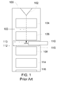
- FIG. 1 shows a diagram of a prior art charged particle beam column used in a typical charged particle beam system for imaging or microfabrication.
- Charged particle source 102 provides charged particles, such as electrons or ions, that are used to form the beam.
- Condenser lens system 104 draws the charged particles from source 102, forms the charged particles into beam 103, and directs beam 103 toward the sample 113.
- Sample 113 is held in a fixed position in sample chamber 115 of column 100 by sample holder 112 and stage 110.
- Objective lens system 106 produces an image of sample 113 based upon the interaction of the charged particles in beam 103 with sample 113.
- some charged particle systems such as a TEM, some of the charged particles in beam 3 pass through sample 113 and are projected by projecting lens system 114 onto viewing device 116 at the bottom of column 100.
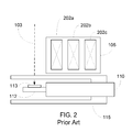
- FIG. 2 shows a cross section view of an objective lens system and a sample chamber of a prior art charged particle beam column.
- the objective lens 106 comprises a plurality of coils 202a-202c that form an electromagnet around the axis of charged particle beam 103.
- Coils 202a-202c of objective lens 106 are often positioned in close proximity to the sample chamber 115.
- the position of stage 110 and sample holder 112 changes relative to the poles of the electromagnet, which causes thermal drift.
- This thermal drift is mainly caused by coils 202a-202c of objective lens 106 being located close to sample chamber 115.
- Coils 202a-202c carry electric current to produce the magnetic field by which objective lens 106 operates.
- the magnification of the system changes, then the amount of ampere-turns changes, which leads to a change in power dissipation and thereby a change in coil-temperature.
- the coil is typically mounted in close proximity to sample chamber 115 and thermal conduction will cause the temperature of sample chamber 115 to change. While the drift may be small, drift becomes more significant as smaller structures are fabricated or imaged.
- One approach to preventing thermal drift is to reduce the heat transfer between the objective coils and the specimen-chamber by insulating them from each other with a layer of stagnant air, which can be a good thermal insulator. But even a layer of stagnant air is not enough to prevent drift.
- Other approaches have included using constant power lenses. But using constant power lenses results in extra power dissipation, oversized coils, spooling of energy and coolwater, and expensive, extremely stable power supplies capable of providing a voltage with a error of less than one part-per-million (“PPM"). For example, a 1000 Volt power supply with an error of 1 PPM (i.e., 0.001 Volt) provides a steady voltage between 999.999 Volts and 1000.001 Volts.
- An object of the invention is to control the transfer of heat between the objective coils and the specimen chamber to reduce or eliminate thermal drift in a charged particle beam system.
- the invention provides a method for reducing drift in a charged particle beam system.
- the method includes providing a charged particle beam column including a charged particle beam, a lens system, and a sample chamber; disposing a temperature-controlled device between the lens system and the sample chamber to control heat transfer between the lens system and the sample chamber; and controlling the temperature of the temperature-controlled device to reduce or eliminate the thermal drift of the position of a sample within the sample chamber relative to the position of the charged particle beam.
- the invention provides an apparatus for reducing drift in a charged particle beam system.
- the apparatus includes a temperature-controlled device disposed between a lens system of a charged particle beam column and a sample chamber of the charged particle beam column; and a temperature controller in thermal communication with the temperature-controlled device, the temperature controller comprising means for controlling heat transfer between the lens system and the sample chamber to reduce or eliminate the thermal drift of charged particle beam.
- the invention provides a charged particle beam system.
- the charged particle beam system includes a charged particle source; a focusing column, the focusing column including a lens system; a sample chamber, the sample chamber including a sample; and a temperature-controlled device disposed between the lens system and the sample chamber to control heat transfer between the lens system and the sample chamber.
- FIG. 1 shows a diagram of a prior art charged particle beam column used in a typical charged particle beam system for imaging or microfabrication
- FIG. 2 shows a cross section view of an objective lens system and a specimen chamber of a prior art charged particle beam column
- FIG. 3 shows a cross section view of an objective lens system and a specimen chamber of a charged particle beam column in accordance with one or more embodiments of the present invention
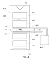
- FIG. 4 shows a diagram of a charged particle beam system suitable for implementing one or more embodiments of the present invention
- a preferred embodiment of the present invention controls the transfer of heat between the objective coils and the specimen chamber to reduce or eliminate thermal drift in a charged particle beam system.
- the charged particle beam may include, but is not limited to, an electron microscope, a scanning electron microscope (SEM), a transmission electron microscope (TEM), a scanning transmission electron microscope (STEM), a focused ion beam system (FIB), or a multiple beam system comprising more than one charged particle beam column.
- SEM scanning electron microscope
- TEM transmission electron microscope
- STEM scanning transmission electron microscope
- FIB focused ion beam system
- the heat transfer can be controlled by making use of the low thermal conductivity between the coil and the sample chamber and stabilize or add a little heat to it in such way the heat transfer is always the same amount.
- a simple and very effective way to control the heat transfer is to place a temperature-controlled device between the objective coil and the sample chamber so that the temperature-controlled device is insulated to both elements.
- the temperature-controlled device is preferably maintained at a constant temperature.
- the temperature-controlled device is preferably positioned to block radiant heat transfer between the objective coil.
- the connection between the sample chamber and the temperature-controlled device is a low thermal conductivity connection. In this way, the sample chamber is surrounded by a temperature-controlled element that is maintained at a constant temperature.
- a high thermal-conductivity disc which is thermally-controlled or stable, can be placed between the sample chamber and the objective coil to reduce drift.
- the high thermal-conductivity disc can be thermally connected to an external device such as a cooling and/or heating system which is external to the charged particle beam column.
- the cooling and/or heating system can be controlled to maintain the high thermal-conductivity disc at a constant temperature. Reducing thermal drift in this manner can substantially reduce the cost and power required compared to prior art methods for reducing thermal drift.
- controlling the temperature of a high thermal conductivity disc in accordance with embodiments of the present invention may require as little as two watts of power and eliminates the need for expensive constant power supplies.
- controlling the temperature of a high thermal conductivity disc in accordance with embodiments of the present invention can reduce the wait time for time to data and wait time due to drift compensation.
- FIG. 3 shows a cross section view of an objective lens system and a sample chamber of a charged particle beam column in accordance with one or more embodiments of the present invention.
- Temperature-controlled device 302 is disposed between objective lens system 106 and sample chamber 115. Temperature-controlled device 302 thermally isolates objective lens system 106 and sample chamber 115 from each other. Temperature-controlled device 302 controls the transfer of heat generated from the electric current in coils 202a-202c to sample chamber 115. Controlling the transfer of heat to sample chamber 115 enables the temperature of sample chamber 115, stage 110, and sample holder 112 to remain substantially constant during operation of the charged particle beam system, even when the current in the coils is changed to change the magnification of the system. Maintaining stage 110 and sample holder 112 at a substantially constant temperature during operation reduces or eliminates drift caused by the expansion or contraction of stage 110 and sample holder 112 relative to the position of charged particle beam 103.
- Temperature-controlled device 302 can be made of any thermally stable material or any thermally conductive material that is capable of directing heat generated by coils 202a-202c of objective lens system 106 away from sample chamber 115.
- temperature-controlled device 302 is mounted in the optical path between objective lens system 106 and sample chamber 110 to reduce or eliminate radiative and/or conductive heat transfer between objective lens system 106 and sample chamber 110.
- Temperature-controlled device 302 is preferably insulated from sample chamber 110 to reduce the heat transfer due to conduction and convection.
- temperature-controlled device 302 can be insulated by an air gap filled with high-R air in the space between sample chamber 110 and temperature-controlled device 302.
- FIG. 4 shows a diagram of a charged particle beam column 400 suitable for implementing one or more embodiments of the present invention.
- Charged particle source 102 provides charged particles, such as electrons or ions, that are used to form the beam.
- Condenser lens system 104 draws the charged particles from source 102, forms the charged particles into beam 103, and directs beam 103 toward the sample 113.
- Sample 113 is held in a fixed position within column 400 by sample holder 112 and stage 110.
- Objective lens system 106 produces an image of sample 113 based upon the interaction of the charged particles in beam 103 with sample 113.
- some charged particle systems such as a TEM, some of the charged particles in beam 103 pass through sample 113 and are projected by projecting lens system 114 onto viewing device 116 at the bottom of column 400.
- Temperature-controlled device 302 is disposed between objective lens system 106 and sample chamber 115 to control heat transfer between objective lens system 106 and sample chamber 115, including stage 110, sample holder 112, and sample 113. Temperature-controlled device 302 is preferably thermally coupled to temperature controller 410. Temperature controller 410 is a device that can be selectively used as a heat sink for the waste heat generated by the coils of objective lens system 106. By selectively directing the waste heat generated by the coils of objective lens system 106 to temperature controller 410 instead of sample chamber 115, sample chamber 115 can be maintained at a substantially constant temperature, reducing or eliminating thermal drift in the position of sample 113 relative to the position of charged particle beam 103.
- Temperature controller 410 maintains temperature controlled device 302 preferably at a temperature no less than 7 degrees Celsius and no more than 35 degrees Celsius, more preferably at a temperature no less than 12 degrees Celsius and no more than 30 degrees Celsius, and most preferably at a temperature no less than 17 degrees Celsius and no more than 25 degrees Celsius. Temperature controller 410 maintains temperature controlled device 302 preferably at a temperature that is no more than 5 degrees Celsius of the temperature of the sample chamber and no less than 5 degrees Celsius of the temperature of the sample chamber. Temperature controller 410 maintains temperature controlled device 302 most preferably at the same temperature as the temperature of the sample chamber.
- temperature controller 410 can also be selectively used as a heat source. By selectively directing the heat generated by temperature controller 410 to the sample chamber 115, sample chamber 115 can be brought up to operating temperature more quickly, thereby reducing the wait time for collecting data. Temperature controller 410 is preferably a device that is external to charged particle column 400.
- temperature controller 410 can be a radiator that conducts waste heat from temperature-controlled device 302 and discharges the waste heat into the ambient air by means of convection or forced convention.
- temperature controller 410 can include a chiller system or a refrigeration system capable of receiving sufficient waste heat from temperature-controlled disc 302 to maintain sample chamber 115 at a substantially constant temperature.
- Temperature controller 410 preferably includes a thermostat or similar device to regulate the temperature of temperature-controlled disc 302. Regulating the temperature of temperature-controlled disc 302 comprises removing waste heat from temperature-controlled disc 302. Regulating the temperature of temperature-controlled disc 302 can also include supplying heat generated by temperature controller 410 to temperature-controlled disc 302.
- temperature-controlled device 402 is disposed between lens system 108 and sample chamber 115 to control heat transfer between lens system 108 and sample chamber 115.
- Temperature-controlled device 302 and temperature-controlled device 402 can both be used in the same system if sample chamber 115 needs to be thermally isolated from lenses or other heat-generating elements that are a source of thermal drift in the system.
- substantially constant temperature means a temperature with no variation, or a temperature with a variation sufficiently small so that there is no thermal drift in the system due to the temperature variation, or a temperature with a variation sufficiently small so that that the thermal drift in the system due to the temperature variation is within acceptable limits for the analysis that is being performed by the system.
- thermal drift is not greater than 0.5 nanometers per minute. In a more preferable embodiment, thermal drift is not greater than 0.1 nanometers per minute.
- a method for reducing drift in a charged particle beam system is comprised of providing a charged particle beam column, which includes a charged particle beam, a lens system, and a sample chamber, disposing a temperature-controlled device between the lens system and the sample chamber to control heat transfer between the lens system and the sample chamber, and controlling the temperature of the temperature-controlled device to reduce or eliminate the thermal drift of the position of a sample disposed within the sample chamber relative to the position of the charged particle beam.
- controlling the temperature of the temperature-controlled device further comprises measuring the temperature of the temperature-controlled device and heating or cooling the temperature-controlled device depending on the temperature.
- controlling the temperature of the temperature-controlled device comprises maintaining the temperature-controlled device at a substantially constant temperature. Yet in some embodiments, controlling the temperature of the temperature-controlled device comprises maintaining the temperature-controlled device at a temperature within 5 degrees Celsius of the temperature of the sample chamber. In some embodiments, controlling the temperature of the temperature-controlled device comprises maintaining the temperature-controlled device at a temperature that is substantially the same as the temperature of the sample chamber.
- maintaining the temperature-controlled device at a substantially constant temperature comprises maintaining the temperature-controlled device between 17 degrees Celsius and 25 degrees Celsius.
- the thermal drift of the particle beam is no more than 0.5 nanometers per minute. Yet in some embodiments, the thermal drift of the particle beam is no more than 0.1 nanometers per minute.
- controlling the temperature of the temperature-controlled device comprises directing heat from the temperature-controlled device to a heat sink. Yet in some embodiments, controlling the temperature of the temperature-controlled device comprises directing heat from a heat source to the temperature-controlled device.
- the method for reducing drift in a charged particle beam system comprises disposing a layer of insulating air between the sample chamber and the temperature-controlled device.
- the charged particle beam system comprises an electron microscope, a scanning electron microscope, a transmission electron microscope, or a focused ion beam system.
- an apparatus for reducing drift in a charged particle beam system comprises a temperature-controlled device disposed between a lens system of a charged particle beam column and a sample chamber of the charged particle beam column and a temperature controller, which comprises means for controlling heat transfer between the lens system and the sample chamber to reduce or eliminate the thermal drift of charged particle beam system, in thermal communication with the temperature-controlled device.
- the temperature controller includes a thermostat and a heat sink.
- the heat sink comprises a radiator that is external to the charged particle beam system and that discharges waste heat into ambient air. Yet in some embodiments, the heat sink comprises a chiller unit or a refrigerator unit that is external to the charged particle beam system.
- the apparatus for reducing drift in a charged particle beam system comprises a layer of insulating air between the sample chamber and the temperature-controlled device.
- the charged particle beam system comprises an electron microscope, a scanning electron microscope, a transmission electron microscope, or a focused ion beam system.
- a charged particle beam system is comprised of a charged particle source, a focusing column which includes a lens system, a sample chamber which includes a sample, and a temperature-controlled device disposed between the lens system and the sample chamber to control heat transfer between the lens system and the sample chamber.
- the charged particle beam system comprises a temperature controller in thermal communication with the temperature-controlled device to control the temperature of the temperature-controlled device.
- the temperature controller includes a thermostat and a heat sink.
- the heat sink comprises a radiator that is external to the charged particle beam system and that discharges waste heat into ambient air.
- the heat sink comprises a chiller unit or a refrigerator unit that is external to the charged particle beam system.
- the charged particle beam system comprises a layer of insulating air disposed between the sample chamber and the temperature-controlled device. Yet in some embodiments, the charged particle beam system comprises an electron microscope, a scanning electron microscope, a transmission electron microscope, or a focused ion beam system.
Landscapes
- Chemical & Material Sciences (AREA)
- Analytical Chemistry (AREA)
- Physics & Mathematics (AREA)
- General Physics & Mathematics (AREA)
- Engineering & Computer Science (AREA)
- Automation & Control Theory (AREA)
- Analysing Materials By The Use Of Radiation (AREA)
- Electron Beam Exposure (AREA)
- Electron Sources, Ion Sources (AREA)
Applications Claiming Priority (1)
| Application Number | Priority Date | Filing Date | Title |
|---|---|---|---|
| US201161580504P | 2011-12-27 | 2011-12-27 |
Publications (2)
| Publication Number | Publication Date |
|---|---|
| EP2610889A2 true EP2610889A2 (de) | 2013-07-03 |
| EP2610889A3 EP2610889A3 (de) | 2015-05-06 |
Family
ID=47563069
Family Applications (1)
| Application Number | Title | Priority Date | Filing Date |
|---|---|---|---|
| EP20120198302 Withdrawn EP2610889A3 (de) | 2011-12-27 | 2012-12-20 | Kontrolle der Drift in einem Strahlsystem geladener Teilchen |
Country Status (4)
| Country | Link |
|---|---|
| US (1) | US8618478B2 (de) |
| EP (1) | EP2610889A3 (de) |
| JP (1) | JP6262428B2 (de) |
| CN (1) | CN103187223B (de) |
Families Citing this family (5)
| Publication number | Priority date | Publication date | Assignee | Title |
|---|---|---|---|---|
| EP3528276A3 (de) * | 2011-05-13 | 2019-09-04 | Fibics Incorporated | Mikroskopiebildgebungsverfahren |
| US8766213B2 (en) | 2012-09-07 | 2014-07-01 | Fei Company | Automated method for coincident alignment of a laser beam and a charged particle beam |
| EP2811288B1 (de) | 2013-06-06 | 2016-08-10 | Fei Company | Verfahren zur Elektronentomographie |
| JP2015153763A (ja) * | 2014-02-10 | 2015-08-24 | 株式会社ニューフレアテクノロジー | 荷電粒子ビーム描画装置および荷電粒子ビーム描画方法 |
| DE102019216791B9 (de) * | 2019-10-30 | 2026-03-05 | Carl Zeiss Microscopy Gmbh | Verfahren zum Betreiben eines Teilchenstrahlgeräts und/oder eines Lichtmikroskops, Computerprogrammprodukt sowie Teilchenstrahlgerät und Lichtmikroskop zur Durchführung des Verfahrens |
Family Cites Families (33)
| Publication number | Priority date | Publication date | Assignee | Title |
|---|---|---|---|---|
| JP2788139B2 (ja) | 1991-09-25 | 1998-08-20 | 株式会社日立製作所 | 電子線描画装置 |
| JPH0689850A (ja) * | 1992-09-09 | 1994-03-29 | Fujitsu Ltd | 電子ビーム露光装置 |
| JP3221797B2 (ja) | 1994-06-14 | 2001-10-22 | 株式会社日立製作所 | 試料作成方法及びその装置 |
| US5916424A (en) | 1996-04-19 | 1999-06-29 | Micrion Corporation | Thin film magnetic recording heads and systems and methods for manufacturing the same |
| US5942805A (en) | 1996-12-20 | 1999-08-24 | Intel Corporation | Fiducial for aligning an integrated circuit die |
| US5847821A (en) | 1997-07-10 | 1998-12-08 | Advanced Micro Devices, Inc. | Use of fiducial marks for improved blank wafer defect review |
| JPH11238483A (ja) * | 1997-12-12 | 1999-08-31 | Hitachi Ltd | 荷電粒子線装置 |
| US6424734B1 (en) | 1998-04-03 | 2002-07-23 | Cognex Corporation | Fiducial mark search using sub-models |
| JP3648384B2 (ja) | 1998-07-03 | 2005-05-18 | 株式会社日立製作所 | 集束イオンビーム加工方法及び加工装置 |
| JP2000133567A (ja) | 1998-10-23 | 2000-05-12 | Advantest Corp | 電子ビーム露光方法及び電子ビーム露光装置 |
| TW460755B (en) | 1998-12-16 | 2001-10-21 | Asm Lithography Bv | Lithographic projection apparatus |
| JP2000268756A (ja) * | 1999-03-12 | 2000-09-29 | Toshiba Corp | 荷電ビーム装置および荷電ビームの制御方法 |
| JP2000277045A (ja) * | 1999-03-24 | 2000-10-06 | Hitachi Ltd | 走査電子顕微鏡 |
| JP2001084935A (ja) * | 1999-09-17 | 2001-03-30 | Hitachi Ltd | 電子顕微鏡 |
| JP4137329B2 (ja) | 2000-01-11 | 2008-08-20 | エスアイアイ・ナノテクノロジー株式会社 | 集束イオンビーム加工方法 |
| US6322672B1 (en) | 2000-03-10 | 2001-11-27 | Fei Company | Method and apparatus for milling copper interconnects in a charged particle beam system |
| US6838380B2 (en) | 2001-01-26 | 2005-01-04 | Fei Company | Fabrication of high resistivity structures using focused ion beams |
| US6570170B2 (en) | 2001-03-01 | 2003-05-27 | Omniprobe, Inc. | Total release method for sample extraction from a charged-particle instrument |
| EP1396228A4 (de) * | 2001-06-07 | 2005-08-10 | Hitachi Medical Corp | Diagnotisches röntgengerät |
| US7160475B2 (en) | 2002-11-21 | 2007-01-09 | Fei Company | Fabrication of three dimensional structures |
| JP2004253232A (ja) | 2003-02-20 | 2004-09-09 | Renesas Technology Corp | 試料固定台 |
| JP4520426B2 (ja) | 2005-07-04 | 2010-08-04 | 株式会社ニューフレアテクノロジー | 電子ビームのビームドリフト補正方法及び電子ビームの描画方法 |
| NL1029982C2 (nl) | 2005-09-19 | 2007-03-20 | Fei Co | Werkwijze voor het instellen van de werkingssfeer van een toestelcomponent op een vooraf vastgesteld element. |
| US7625679B2 (en) | 2005-09-23 | 2009-12-01 | Applied Materials, Inc. | Method of aligning a particle-beam-generated pattern to a pattern on a pre-patterned substrate |
| US7660687B1 (en) | 2006-05-25 | 2010-02-09 | Kla-Tencor Corporation | Robust measurement of parameters |
| JP4719628B2 (ja) * | 2006-06-13 | 2011-07-06 | 株式会社日立ハイテクノロジーズ | 走査電子顕微鏡 |
| US7880155B2 (en) | 2006-06-15 | 2011-02-01 | Brooks Automation, Inc. | Substrate alignment apparatus comprising a controller to measure alignment during transport |
| EP2104946B1 (de) | 2006-10-20 | 2015-08-12 | FEI Company | Verfahren zur erstellung einer stammzellenprobe und einer probenstruktur |
| US7601955B2 (en) * | 2007-09-04 | 2009-10-13 | Visera Technologies Company Limited | Scanning electron microscope |
| US7880151B2 (en) | 2008-02-28 | 2011-02-01 | Fei Company | Beam positioning for beam processing |
| JP2009218474A (ja) * | 2008-03-12 | 2009-09-24 | Jeol Ltd | ビーム位置ドリフト抑制方法、ビーム寸法ドリフト抑制方法及び荷電粒子ビーム描画装置。 |
| JP5386934B2 (ja) * | 2008-11-04 | 2014-01-15 | 株式会社島津製作所 | 荷電粒子ビーム装置及びその対物レンズのコンタミネーション防止装置 |
| EP2430432A4 (de) * | 2009-05-15 | 2014-07-23 | Fei Co | Elektronenmikroskop mit einem oder mehreren integrierten detektoren |
-
2012
- 2012-12-20 EP EP20120198302 patent/EP2610889A3/de not_active Withdrawn
- 2012-12-21 US US13/724,323 patent/US8618478B2/en active Active
- 2012-12-22 JP JP2012280352A patent/JP6262428B2/ja active Active
- 2012-12-27 CN CN201210577853.2A patent/CN103187223B/zh active Active
Non-Patent Citations (1)
| Title |
|---|
| None |
Also Published As
| Publication number | Publication date |
|---|---|
| JP6262428B2 (ja) | 2018-01-17 |
| CN103187223A (zh) | 2013-07-03 |
| US20130200270A1 (en) | 2013-08-08 |
| CN103187223B (zh) | 2018-11-16 |
| US8618478B2 (en) | 2013-12-31 |
| JP2013138007A (ja) | 2013-07-11 |
| EP2610889A3 (de) | 2015-05-06 |
Similar Documents
| Publication | Publication Date | Title |
|---|---|---|
| JP4171479B2 (ja) | 荷電粒子線応用装置及び荷電粒子線応用方法 | |
| US8618478B2 (en) | Drift control in a charged particle beam system | |
| JP5227643B2 (ja) | 高分解能でかつ高コントラストな観察が可能な電子線応用装置 | |
| US20090152462A1 (en) | Gas field ionization ion source, scanning charged particle microscope, optical axis adjustment method and specimen observation method | |
| US6949756B2 (en) | Shaped and low density focused ion beams | |
| NL1023260C1 (nl) | Deeltjes-optisch apparaat met een permanent magnetische lens en een elektrostatische lens. | |
| CN116313708A (zh) | 使用多个带电粒子射束的装置 | |
| TW201527745A (zh) | 用於高產量電子束檢測(ebi)的多射束系統 | |
| JP2009193963A (ja) | 収差補正器及び位相板を備えたtem | |
| JP7190586B2 (ja) | 試料ホルダ、試料ホルダの使用方法、突出量調整治具、突出量の調整方法および荷電粒子線装置 | |
| US9761412B2 (en) | Ion milling apparatus and sample processing method | |
| EP3594988B1 (de) | Hochleistungsfähige rasterelektronenmikroskopvorrichtung für inspektion und verfahren zum betrieb davon | |
| US20130105108A1 (en) | Heat Removal From Substrates In Vacuum | |
| JP2008171774A (ja) | 電子顕微鏡 | |
| WO2014119351A1 (ja) | イオンミリング装置、及びイオンミリング加工方法 | |
| JP2015204181A (ja) | イオンビーム装置 | |
| JP6161430B2 (ja) | 電子レンズ及び荷電粒子線装置 | |
| JP6568627B2 (ja) | イオンビーム装置 | |
| US20080135786A1 (en) | Adjustable aperture element for particle beam device, method of operating and manufacturing thereof | |
| US5736742A (en) | Objective lens and charged particle beam system | |
| US11347043B2 (en) | Operating a particle beam apparatus and/or a light microscope | |
| JP5544439B2 (ja) | 荷電粒子線装置 | |
| JP6134859B2 (ja) | 試料観察方法及び荷電粒子線装置 | |
| TWI761811B (zh) | 功率單元及將功率供應至一電流源負載件之方法 | |
| EP4220680A1 (de) | Vorrichtung mit geladenem teilchenstrahl zur diffraktionsanalyse |
Legal Events
| Date | Code | Title | Description |
|---|---|---|---|
| PUAI | Public reference made under article 153(3) epc to a published international application that has entered the european phase |
Free format text: ORIGINAL CODE: 0009012 |
|
| AK | Designated contracting states |
Kind code of ref document: A2 Designated state(s): AL AT BE BG CH CY CZ DE DK EE ES FI FR GB GR HR HU IE IS IT LI LT LU LV MC MK MT NL NO PL PT RO RS SE SI SK SM TR |
|
| AX | Request for extension of the european patent |
Extension state: BA ME |
|
| RIC1 | Information provided on ipc code assigned before grant |
Ipc: H01J 37/16 20060101AFI20141216BHEP Ipc: H01J 37/26 20060101ALI20141216BHEP Ipc: H01J 37/02 20060101ALI20141216BHEP |
|
| PUAL | Search report despatched |
Free format text: ORIGINAL CODE: 0009013 |
|
| AK | Designated contracting states |
Kind code of ref document: A3 Designated state(s): AL AT BE BG CH CY CZ DE DK EE ES FI FR GB GR HR HU IE IS IT LI LT LU LV MC MK MT NL NO PL PT RO RS SE SI SK SM TR |
|
| AX | Request for extension of the european patent |
Extension state: BA ME |
|
| RIC1 | Information provided on ipc code assigned before grant |
Ipc: H01J 37/02 20060101ALI20150405BHEP Ipc: H01J 37/26 20060101ALI20150405BHEP Ipc: H01J 37/16 20060101AFI20150405BHEP |
|
| STAA | Information on the status of an ep patent application or granted ep patent |
Free format text: STATUS: THE APPLICATION IS DEEMED TO BE WITHDRAWN |
|
| 18D | Application deemed to be withdrawn |
Effective date: 20151107 |