EP2576860B1 - Procédé de traitement thermique latéral de films minces sur des substrats à basse température - Google Patents
Procédé de traitement thermique latéral de films minces sur des substrats à basse température Download PDFInfo
- Publication number
- EP2576860B1 EP2576860B1 EP11790412.8A EP11790412A EP2576860B1 EP 2576860 B1 EP2576860 B1 EP 2576860B1 EP 11790412 A EP11790412 A EP 11790412A EP 2576860 B1 EP2576860 B1 EP 2576860B1
- Authority
- EP
- European Patent Office
- Prior art keywords
- thin film
- substrate
- absorbing
- film
- traces
- Prior art date
- Legal status (The legal status is an assumption and is not a legal conclusion. Google has not performed a legal analysis and makes no representation as to the accuracy of the status listed.)
- Not-in-force
Links
- 239000010409 thin film Substances 0.000 title claims description 102
- 239000000758 substrate Substances 0.000 title claims description 53
- 238000000034 method Methods 0.000 title claims description 47
- 230000005855 radiation Effects 0.000 claims description 23
- 238000003892 spreading Methods 0.000 claims description 22
- 239000000919 ceramic Substances 0.000 claims description 7
- 238000000059 patterning Methods 0.000 claims description 3
- 230000001678 irradiating effect Effects 0.000 claims 1
- 239000010408 film Substances 0.000 description 41
- 229910021417 amorphous silicon Inorganic materials 0.000 description 18
- 239000004065 semiconductor Substances 0.000 description 11
- 239000000463 material Substances 0.000 description 10
- PCHJSUWPFVWCPO-UHFFFAOYSA-N gold Chemical compound [Au] PCHJSUWPFVWCPO-UHFFFAOYSA-N 0.000 description 6
- 239000010931 gold Substances 0.000 description 6
- 229910052737 gold Inorganic materials 0.000 description 6
- 238000010438 heat treatment Methods 0.000 description 6
- 238000000576 coating method Methods 0.000 description 5
- 239000004642 Polyimide Substances 0.000 description 4
- 238000000137 annealing Methods 0.000 description 4
- 238000001723 curing Methods 0.000 description 4
- 229920001721 polyimide Polymers 0.000 description 4
- 238000001237 Raman spectrum Methods 0.000 description 3
- 229910052454 barium strontium titanate Inorganic materials 0.000 description 3
- 230000008901 benefit Effects 0.000 description 3
- 239000011248 coating agent Substances 0.000 description 3
- 238000010894 electron beam technology Methods 0.000 description 3
- 239000002184 metal Substances 0.000 description 3
- 229910052751 metal Inorganic materials 0.000 description 3
- XUIMIQQOPSSXEZ-UHFFFAOYSA-N Silicon Chemical compound [Si] XUIMIQQOPSSXEZ-UHFFFAOYSA-N 0.000 description 2
- 239000004964 aerogel Substances 0.000 description 2
- 239000005388 borosilicate glass Substances 0.000 description 2
- 238000006243 chemical reaction Methods 0.000 description 2
- 230000000694 effects Effects 0.000 description 2
- 238000011067 equilibration Methods 0.000 description 2
- 230000005669 field effect Effects 0.000 description 2
- 230000006698 induction Effects 0.000 description 2
- 238000002347 injection Methods 0.000 description 2
- 239000007924 injection Substances 0.000 description 2
- 229910044991 metal oxide Inorganic materials 0.000 description 2
- 150000004706 metal oxides Chemical class 0.000 description 2
- 230000003071 parasitic effect Effects 0.000 description 2
- 239000002245 particle Substances 0.000 description 2
- 238000003672 processing method Methods 0.000 description 2
- 229910052710 silicon Inorganic materials 0.000 description 2
- 239000010703 silicon Substances 0.000 description 2
- VYPSYNLAJGMNEJ-UHFFFAOYSA-N silicon dioxide Inorganic materials O=[Si]=O VYPSYNLAJGMNEJ-UHFFFAOYSA-N 0.000 description 2
- 238000005245 sintering Methods 0.000 description 2
- 239000004965 Silica aerogel Substances 0.000 description 1
- BQCADISMDOOEFD-UHFFFAOYSA-N Silver Chemical compound [Ag] BQCADISMDOOEFD-UHFFFAOYSA-N 0.000 description 1
- 230000004888 barrier function Effects 0.000 description 1
- 229910021419 crystalline silicon Inorganic materials 0.000 description 1
- 238000002425 crystallisation Methods 0.000 description 1
- 230000008025 crystallization Effects 0.000 description 1
- 238000007872 degassing Methods 0.000 description 1
- 230000002939 deleterious effect Effects 0.000 description 1
- 230000008021 deposition Effects 0.000 description 1
- 239000003989 dielectric material Substances 0.000 description 1
- 238000009792 diffusion process Methods 0.000 description 1
- 239000002019 doping agent Substances 0.000 description 1
- 238000001035 drying Methods 0.000 description 1
- 230000005684 electric field Effects 0.000 description 1
- 239000011521 glass Substances 0.000 description 1
- 230000000977 initiatory effect Effects 0.000 description 1
- 238000002955 isolation Methods 0.000 description 1
- 238000004519 manufacturing process Methods 0.000 description 1
- 239000011159 matrix material Substances 0.000 description 1
- 150000002739 metals Chemical class 0.000 description 1
- 229910021424 microcrystalline silicon Inorganic materials 0.000 description 1
- 238000004377 microelectronic Methods 0.000 description 1
- 239000005543 nano-size silicon particle Substances 0.000 description 1
- 239000002105 nanoparticle Substances 0.000 description 1
- 239000004033 plastic Substances 0.000 description 1
- 229920003207 poly(ethylene-2,6-naphthalate) Polymers 0.000 description 1
- 239000004417 polycarbonate Substances 0.000 description 1
- 229920000515 polycarbonate Polymers 0.000 description 1
- 239000011112 polyethylene naphthalate Substances 0.000 description 1
- 229920000139 polyethylene terephthalate Polymers 0.000 description 1
- 239000005020 polyethylene terephthalate Substances 0.000 description 1
- 229920000642 polymer Polymers 0.000 description 1
- 238000006116 polymerization reaction Methods 0.000 description 1
- 238000010926 purge Methods 0.000 description 1
- 239000010453 quartz Substances 0.000 description 1
- 238000000926 separation method Methods 0.000 description 1
- 229910052709 silver Inorganic materials 0.000 description 1
- 239000004332 silver Substances 0.000 description 1
- HUAUNKAZQWMVFY-UHFFFAOYSA-M sodium;oxocalcium;hydroxide Chemical compound [OH-].[Na+].[Ca]=O HUAUNKAZQWMVFY-UHFFFAOYSA-M 0.000 description 1
- 238000012360 testing method Methods 0.000 description 1
Images


Classifications
-
- H—ELECTRICITY
- H01—ELECTRIC ELEMENTS
- H01L—SEMICONDUCTOR DEVICES NOT COVERED BY CLASS H10
- H01L21/00—Processes or apparatus adapted for the manufacture or treatment of semiconductor or solid state devices or of parts thereof
- H01L21/02—Manufacture or treatment of semiconductor devices or of parts thereof
- H01L21/04—Manufacture or treatment of semiconductor devices or of parts thereof the devices having at least one potential-jump barrier or surface barrier, e.g. PN junction, depletion layer or carrier concentration layer
- H01L21/18—Manufacture or treatment of semiconductor devices or of parts thereof the devices having at least one potential-jump barrier or surface barrier, e.g. PN junction, depletion layer or carrier concentration layer the devices having semiconductor bodies comprising elements of Group IV of the Periodic System or AIIIBV compounds with or without impurities, e.g. doping materials
- H01L21/26—Bombardment with radiation
- H01L21/263—Bombardment with radiation with high-energy radiation
- H01L21/268—Bombardment with radiation with high-energy radiation using electromagnetic radiation, e.g. laser radiation
-
- H—ELECTRICITY
- H01—ELECTRIC ELEMENTS
- H01L—SEMICONDUCTOR DEVICES NOT COVERED BY CLASS H10
- H01L21/00—Processes or apparatus adapted for the manufacture or treatment of semiconductor or solid state devices or of parts thereof
- H01L21/02—Manufacture or treatment of semiconductor devices or of parts thereof
- H01L21/04—Manufacture or treatment of semiconductor devices or of parts thereof the devices having at least one potential-jump barrier or surface barrier, e.g. PN junction, depletion layer or carrier concentration layer
- H01L21/34—Manufacture or treatment of semiconductor devices or of parts thereof the devices having at least one potential-jump barrier or surface barrier, e.g. PN junction, depletion layer or carrier concentration layer the devices having semiconductor bodies not provided for in groups H01L21/0405, H01L21/0445, H01L21/06, H01L21/16 and H01L21/18 with or without impurities, e.g. doping materials
- H01L21/42—Bombardment with radiation
- H01L21/423—Bombardment with radiation with high-energy radiation
- H01L21/428—Bombardment with radiation with high-energy radiation using electromagnetic radiation, e.g. laser radiation
-
- B—PERFORMING OPERATIONS; TRANSPORTING
- B29—WORKING OF PLASTICS; WORKING OF SUBSTANCES IN A PLASTIC STATE IN GENERAL
- B29C—SHAPING OR JOINING OF PLASTICS; SHAPING OF MATERIAL IN A PLASTIC STATE, NOT OTHERWISE PROVIDED FOR; AFTER-TREATMENT OF THE SHAPED PRODUCTS, e.g. REPAIRING
- B29C35/00—Heating, cooling or curing, e.g. crosslinking or vulcanising; Apparatus therefor
- B29C35/02—Heating or curing, e.g. crosslinking or vulcanizing during moulding, e.g. in a mould
- B29C35/0266—Local curing
-
- B—PERFORMING OPERATIONS; TRANSPORTING
- B29—WORKING OF PLASTICS; WORKING OF SUBSTANCES IN A PLASTIC STATE IN GENERAL
- B29C—SHAPING OR JOINING OF PLASTICS; SHAPING OF MATERIAL IN A PLASTIC STATE, NOT OTHERWISE PROVIDED FOR; AFTER-TREATMENT OF THE SHAPED PRODUCTS, e.g. REPAIRING
- B29C35/00—Heating, cooling or curing, e.g. crosslinking or vulcanising; Apparatus therefor
- B29C35/02—Heating or curing, e.g. crosslinking or vulcanizing during moulding, e.g. in a mould
- B29C35/0272—Heating or curing, e.g. crosslinking or vulcanizing during moulding, e.g. in a mould using lost heating elements, i.e. heating means incorporated and remaining in the formed article
-
- H—ELECTRICITY
- H01—ELECTRIC ELEMENTS
- H01L—SEMICONDUCTOR DEVICES NOT COVERED BY CLASS H10
- H01L21/00—Processes or apparatus adapted for the manufacture or treatment of semiconductor or solid state devices or of parts thereof
- H01L21/02—Manufacture or treatment of semiconductor devices or of parts thereof
- H01L21/02104—Forming layers
- H01L21/02365—Forming inorganic semiconducting materials on a substrate
- H01L21/02367—Substrates
- H01L21/0237—Materials
- H01L21/02422—Non-crystalline insulating materials, e.g. glass, polymers
-
- H—ELECTRICITY
- H01—ELECTRIC ELEMENTS
- H01L—SEMICONDUCTOR DEVICES NOT COVERED BY CLASS H10
- H01L21/00—Processes or apparatus adapted for the manufacture or treatment of semiconductor or solid state devices or of parts thereof
- H01L21/02—Manufacture or treatment of semiconductor devices or of parts thereof
- H01L21/02104—Forming layers
- H01L21/02365—Forming inorganic semiconducting materials on a substrate
- H01L21/02436—Intermediate layers between substrates and deposited layers
- H01L21/02439—Materials
-
- H—ELECTRICITY
- H01—ELECTRIC ELEMENTS
- H01L—SEMICONDUCTOR DEVICES NOT COVERED BY CLASS H10
- H01L21/00—Processes or apparatus adapted for the manufacture or treatment of semiconductor or solid state devices or of parts thereof
- H01L21/02—Manufacture or treatment of semiconductor devices or of parts thereof
- H01L21/02104—Forming layers
- H01L21/02365—Forming inorganic semiconducting materials on a substrate
- H01L21/02518—Deposited layers
- H01L21/02521—Materials
- H01L21/02524—Group 14 semiconducting materials
- H01L21/02532—Silicon, silicon germanium, germanium
-
- H—ELECTRICITY
- H01—ELECTRIC ELEMENTS
- H01L—SEMICONDUCTOR DEVICES NOT COVERED BY CLASS H10
- H01L21/00—Processes or apparatus adapted for the manufacture or treatment of semiconductor or solid state devices or of parts thereof
- H01L21/02—Manufacture or treatment of semiconductor devices or of parts thereof
- H01L21/02104—Forming layers
- H01L21/02365—Forming inorganic semiconducting materials on a substrate
- H01L21/02656—Special treatments
- H01L21/02664—Aftertreatments
- H01L21/02667—Crystallisation or recrystallisation of non-monocrystalline semiconductor materials, e.g. regrowth
- H01L21/02675—Crystallisation or recrystallisation of non-monocrystalline semiconductor materials, e.g. regrowth using laser beams
- H01L21/02686—Pulsed laser beam
-
- H—ELECTRICITY
- H01—ELECTRIC ELEMENTS
- H01L—SEMICONDUCTOR DEVICES NOT COVERED BY CLASS H10
- H01L21/00—Processes or apparatus adapted for the manufacture or treatment of semiconductor or solid state devices or of parts thereof
- H01L21/02—Manufacture or treatment of semiconductor devices or of parts thereof
- H01L21/02104—Forming layers
- H01L21/02365—Forming inorganic semiconducting materials on a substrate
- H01L21/02656—Special treatments
- H01L21/02664—Aftertreatments
- H01L21/02667—Crystallisation or recrystallisation of non-monocrystalline semiconductor materials, e.g. regrowth
- H01L21/02689—Crystallisation or recrystallisation of non-monocrystalline semiconductor materials, e.g. regrowth using particle beams
-
- H—ELECTRICITY
- H01—ELECTRIC ELEMENTS
- H01L—SEMICONDUCTOR DEVICES NOT COVERED BY CLASS H10
- H01L27/00—Devices consisting of a plurality of semiconductor or other solid-state components formed in or on a common substrate
- H01L27/02—Devices consisting of a plurality of semiconductor or other solid-state components formed in or on a common substrate including semiconductor components specially adapted for rectifying, oscillating, amplifying or switching and having at least one potential-jump barrier or surface barrier; including integrated passive circuit elements with at least one potential-jump barrier or surface barrier
- H01L27/12—Devices consisting of a plurality of semiconductor or other solid-state components formed in or on a common substrate including semiconductor components specially adapted for rectifying, oscillating, amplifying or switching and having at least one potential-jump barrier or surface barrier; including integrated passive circuit elements with at least one potential-jump barrier or surface barrier the substrate being other than a semiconductor body, e.g. an insulating body
- H01L27/1214—Devices consisting of a plurality of semiconductor or other solid-state components formed in or on a common substrate including semiconductor components specially adapted for rectifying, oscillating, amplifying or switching and having at least one potential-jump barrier or surface barrier; including integrated passive circuit elements with at least one potential-jump barrier or surface barrier the substrate being other than a semiconductor body, e.g. an insulating body comprising a plurality of TFTs formed on a non-semiconducting substrate, e.g. driving circuits for AMLCDs
- H01L27/1259—Multistep manufacturing methods
- H01L27/127—Multistep manufacturing methods with a particular formation, treatment or patterning of the active layer specially adapted to the circuit arrangement
- H01L27/1274—Multistep manufacturing methods with a particular formation, treatment or patterning of the active layer specially adapted to the circuit arrangement using crystallisation of amorphous semiconductor or recrystallisation of crystalline semiconductor
- H01L27/1281—Multistep manufacturing methods with a particular formation, treatment or patterning of the active layer specially adapted to the circuit arrangement using crystallisation of amorphous semiconductor or recrystallisation of crystalline semiconductor by using structural features to control crystal growth, e.g. placement of grain filters
-
- H—ELECTRICITY
- H01—ELECTRIC ELEMENTS
- H01L—SEMICONDUCTOR DEVICES NOT COVERED BY CLASS H10
- H01L27/00—Devices consisting of a plurality of semiconductor or other solid-state components formed in or on a common substrate
- H01L27/02—Devices consisting of a plurality of semiconductor or other solid-state components formed in or on a common substrate including semiconductor components specially adapted for rectifying, oscillating, amplifying or switching and having at least one potential-jump barrier or surface barrier; including integrated passive circuit elements with at least one potential-jump barrier or surface barrier
- H01L27/12—Devices consisting of a plurality of semiconductor or other solid-state components formed in or on a common substrate including semiconductor components specially adapted for rectifying, oscillating, amplifying or switching and having at least one potential-jump barrier or surface barrier; including integrated passive circuit elements with at least one potential-jump barrier or surface barrier the substrate being other than a semiconductor body, e.g. an insulating body
- H01L27/1214—Devices consisting of a plurality of semiconductor or other solid-state components formed in or on a common substrate including semiconductor components specially adapted for rectifying, oscillating, amplifying or switching and having at least one potential-jump barrier or surface barrier; including integrated passive circuit elements with at least one potential-jump barrier or surface barrier the substrate being other than a semiconductor body, e.g. an insulating body comprising a plurality of TFTs formed on a non-semiconducting substrate, e.g. driving circuits for AMLCDs
- H01L27/1259—Multistep manufacturing methods
- H01L27/127—Multistep manufacturing methods with a particular formation, treatment or patterning of the active layer specially adapted to the circuit arrangement
- H01L27/1274—Multistep manufacturing methods with a particular formation, treatment or patterning of the active layer specially adapted to the circuit arrangement using crystallisation of amorphous semiconductor or recrystallisation of crystalline semiconductor
- H01L27/1285—Multistep manufacturing methods with a particular formation, treatment or patterning of the active layer specially adapted to the circuit arrangement using crystallisation of amorphous semiconductor or recrystallisation of crystalline semiconductor using control of the annealing or irradiation parameters, e.g. using different scanning direction or intensity for different transistors
-
- H—ELECTRICITY
- H01—ELECTRIC ELEMENTS
- H01L—SEMICONDUCTOR DEVICES NOT COVERED BY CLASS H10
- H01L29/00—Semiconductor devices adapted for rectifying, amplifying, oscillating or switching, or capacitors or resistors with at least one potential-jump barrier or surface barrier, e.g. PN junction depletion layer or carrier concentration layer; Details of semiconductor bodies or of electrodes thereof ; Multistep manufacturing processes therefor
- H01L29/66—Types of semiconductor device ; Multistep manufacturing processes therefor
- H01L29/66007—Multistep manufacturing processes
- H01L29/66075—Multistep manufacturing processes of devices having semiconductor bodies comprising group 14 or group 13/15 materials
- H01L29/66227—Multistep manufacturing processes of devices having semiconductor bodies comprising group 14 or group 13/15 materials the devices being controllable only by the electric current supplied or the electric potential applied, to an electrode which does not carry the current to be rectified, amplified or switched, e.g. three-terminal devices
- H01L29/66409—Unipolar field-effect transistors
- H01L29/66477—Unipolar field-effect transistors with an insulated gate, i.e. MISFET
- H01L29/66742—Thin film unipolar transistors
- H01L29/6675—Amorphous silicon or polysilicon transistors
- H01L29/66757—Lateral single gate single channel transistors with non-inverted structure, i.e. the channel layer is formed before the gate
-
- H—ELECTRICITY
- H01—ELECTRIC ELEMENTS
- H01L—SEMICONDUCTOR DEVICES NOT COVERED BY CLASS H10
- H01L29/00—Semiconductor devices adapted for rectifying, amplifying, oscillating or switching, or capacitors or resistors with at least one potential-jump barrier or surface barrier, e.g. PN junction depletion layer or carrier concentration layer; Details of semiconductor bodies or of electrodes thereof ; Multistep manufacturing processes therefor
- H01L29/66—Types of semiconductor device ; Multistep manufacturing processes therefor
- H01L29/68—Types of semiconductor device ; Multistep manufacturing processes therefor controllable by only the electric current supplied, or only the electric potential applied, to an electrode which does not carry the current to be rectified, amplified or switched
- H01L29/76—Unipolar devices, e.g. field effect transistors
- H01L29/772—Field effect transistors
- H01L29/78—Field effect transistors with field effect produced by an insulated gate
- H01L29/786—Thin film transistors, i.e. transistors with a channel being at least partly a thin film
- H01L29/78603—Thin film transistors, i.e. transistors with a channel being at least partly a thin film characterised by the insulating substrate or support
-
- B—PERFORMING OPERATIONS; TRANSPORTING
- B29—WORKING OF PLASTICS; WORKING OF SUBSTANCES IN A PLASTIC STATE IN GENERAL
- B29C—SHAPING OR JOINING OF PLASTICS; SHAPING OF MATERIAL IN A PLASTIC STATE, NOT OTHERWISE PROVIDED FOR; AFTER-TREATMENT OF THE SHAPED PRODUCTS, e.g. REPAIRING
- B29C35/00—Heating, cooling or curing, e.g. crosslinking or vulcanising; Apparatus therefor
- B29C35/02—Heating or curing, e.g. crosslinking or vulcanizing during moulding, e.g. in a mould
- B29C35/08—Heating or curing, e.g. crosslinking or vulcanizing during moulding, e.g. in a mould by wave energy or particle radiation
- B29C35/0805—Heating or curing, e.g. crosslinking or vulcanizing during moulding, e.g. in a mould by wave energy or particle radiation using electromagnetic radiation
- B29C2035/0855—Heating or curing, e.g. crosslinking or vulcanizing during moulding, e.g. in a mould by wave energy or particle radiation using electromagnetic radiation using microwave
-
- B—PERFORMING OPERATIONS; TRANSPORTING
- B29—WORKING OF PLASTICS; WORKING OF SUBSTANCES IN A PLASTIC STATE IN GENERAL
- B29C—SHAPING OR JOINING OF PLASTICS; SHAPING OF MATERIAL IN A PLASTIC STATE, NOT OTHERWISE PROVIDED FOR; AFTER-TREATMENT OF THE SHAPED PRODUCTS, e.g. REPAIRING
- B29C35/00—Heating, cooling or curing, e.g. crosslinking or vulcanising; Apparatus therefor
- B29C35/02—Heating or curing, e.g. crosslinking or vulcanizing during moulding, e.g. in a mould
- B29C35/08—Heating or curing, e.g. crosslinking or vulcanizing during moulding, e.g. in a mould by wave energy or particle radiation
- B29C35/0866—Heating or curing, e.g. crosslinking or vulcanizing during moulding, e.g. in a mould by wave energy or particle radiation using particle radiation
- B29C2035/0877—Heating or curing, e.g. crosslinking or vulcanizing during moulding, e.g. in a mould by wave energy or particle radiation using particle radiation using electron radiation, e.g. beta-rays
-
- B—PERFORMING OPERATIONS; TRANSPORTING
- B29—WORKING OF PLASTICS; WORKING OF SUBSTANCES IN A PLASTIC STATE IN GENERAL
- B29C—SHAPING OR JOINING OF PLASTICS; SHAPING OF MATERIAL IN A PLASTIC STATE, NOT OTHERWISE PROVIDED FOR; AFTER-TREATMENT OF THE SHAPED PRODUCTS, e.g. REPAIRING
- B29C35/00—Heating, cooling or curing, e.g. crosslinking or vulcanising; Apparatus therefor
- B29C35/02—Heating or curing, e.g. crosslinking or vulcanizing during moulding, e.g. in a mould
- B29C35/08—Heating or curing, e.g. crosslinking or vulcanizing during moulding, e.g. in a mould by wave energy or particle radiation
- B29C35/0805—Heating or curing, e.g. crosslinking or vulcanizing during moulding, e.g. in a mould by wave energy or particle radiation using electromagnetic radiation
Definitions
- the present invention relates to a method for curing thin films on substrates in general, and, in particular, to a method for thermally processing thin films on low-temperature substrates.
- thermal processing encompasses sintering, annealing, curing, drying, crystallization, polymerization, chemical reaction initiation and modulation, dopant drive-in, degasification, etc.
- Thermal processing of semiconductor thin films is typically performed in high temperature environments. For example, amorphous silicon (a-Si) is annealed at 1,100 °C, and silicon nanoparticle films are sintered at 900 °C.
- a-Si amorphous silicon
- silicon nanoparticle films are sintered at 900 °C.
- US-5,950,078 discloses a method for rapid thermally annealing a thin amorphous film.
- low-temperature substrates such as borosilicate or soda lime
- substrates such as borosilicate or soda lime
- plastic i.e., polycarbonate, polyimide, PET, PEN, etc.
- paper because their cost is even lower.
- the present disclosure provides a method for thermally processing thin films on low-temperature substrates.
- the pulsed radiation emitted from flashlamps, directed plasma arcs (DPAs), lasers, microwaves, induction heaters or electron beams has the ability to preferentially heat the thin film over its substrate.
- DPAs directed plasma arcs
- the substrate can serve as a heat sink to rapidly cool the thin film immediately after thermal processing.
- pulsed radiation thermal processing allows a thin film to be heated to a much higher temperature than its substrate can normally withstand at thermal equilibrium
- thermal processing technique generally depends on the ability of a thin film to absorb the radiation that is used to heat the thin film.
- a thin film is very thin and/or somewhat transparent, it is quite difficult to thermally process the very thin film directly with the pulsed radiation thermal processing technique because the very thin film typically absorbs minimal radiation. Consequently, an improved method is required to thermally process a very thin film.
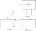
- a very thin film 12 is deposited on a substrate 14 via well-known vacuum techniques. Very thin film 12 may also be coated or printed on substrate 14 . Very thin film 12 can be a fully dense film or a particulate film. The thickness of very thin film 12 is preferably less than 10 microns.
- an absorbing trace 11 is deposited on top of very thin film 12 to form a thin film stack 10 , as shown in Figure 1a . Absorbing trace 11 is preferably made of a material that is more absorptive of pulsed radiation than very thin film 12 . Examples of absorbing trace 11 include metals or ceramics.
- absorbing trace 11 is preferentially heated before very thin film 12 .
- Light source 15 can be a flashlamp, directed plasma arc (DPA), laser, microwave generator, induction heater or electron beam.
- DPA directed plasma arc
- the area (shaded area) within very thin film 12 and substrate 14 located underneath and adjacent to absorbing trace 11 is thermally processed by the heated absorbing trace 11 , as shown in Figure 1b .
- the distance d 1 within very thin film 12 that is thermally processed can be tens of microns.
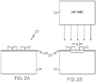
- a very thin film 23 is deposited on a substrate 24 via well-known vacuum techniques.
- Very thin film 23 can also be coated or printed on substrate 24 .
- Very thin film 23 can be a fully dense film or a particulate film.
- the thickness of very thin film 23 is preferably less than 10 microns.
- absorbing traces 21, 22 are deposited on very thin film 23 to form a thin film stack 20 , as shown in Figure 2a .
- absorbing traces 21 , 22 are made of a material that is more absorptive of pulsed radiation than very thin film 23 .
- the absorbing traces 21 , 22 are made of ceramics.
- the absorbing traces 21 , 22 are formed on top of very thin film 23 .
- absorbing traces 21 , 22 are preferentially heated over very thin film 23 .
- the heat from absorbing traces 21 , 22 is then conducted to the area of very thin film 23 underneath and/or adjacent to absorbing traces 21 , 22 , as shown in Figure 2b .
- an area d 2 within very thin film 23 located between absorbing traces 21 , 22 becomes thermally processed.
- the gap distance that can be thermally processed between absorbing traces 21 and 22 i.e., area d 2
- the gap distance that can be thermally processed between absorbing traces 21 and 22 is generally larger than d 1 from Figure 1b since it is the overlap of the heat being conducted by two absorbing traces 21 , 22 and is preferably less than 100 microns.
- very thin film 23 tends to be more uniformly processed than the area of a thin film adjacent to only one absorbing trace (such as in Figure 1b ).
- Substrate 14 in Figures 1a-1b and substrate 24 in Figures 2a-2b are preferably high-temperature substrates.
- thermal processing of very thin films can also be performed on low-temperature substrates (i.e., maximum working temperatures of 150 °C or less) by applying heat spreading films before or after the application of the absorbing traces. Since the thermal conductivity of the heat spreading film is higher than that of the low temperature substrate, heat is preferentially conducted in the plane of the very thin film and the heat spreading film instead of the low temperature substrate after absorbing traces have been heated.
- the heat spreading film also acts as a thermal barrier layer to protect the low temperature substrate.
- the preferential conduction of heat in the plane of the very thin film increases the distance at which absorbing traces can be placed from each other.
- the heat spreading film is generally thicker than the very thin film and is generally transparent to the light used to heat the absorbing traces.
- a heat spreading film 35 is deposited on a substrate 34 via well-known vacuum techniques. Heat spreading film 35 may be coated or printed on substrate 34 . A very thin film 33 is then deposited on top of heat spreading film 35 via well-known vacuum techniques. Very thin film 33 may be coated or printed on heat spreading film 35 . Very thin film 33 can be a fully dense film or a particulate film. The thickness of very thin film 33 is preferably less than 10 microns.
- absorbing traces 31, 32 are deposited on very thin film 33 to form a thin film stack 30 , as shown in Figure 3a .
- absorbing traces 31 , 32 are made of a material that is more absorptive of pulsed radiation than very thin film 33 .
- Examples of absorbing traces 31 , 3 2 are made of ceramics.
- the absorbing traces 31 , 32 are formed on top of very thin film 33.
- heat spreading film 35 is shown to be formed underneath very thin film 33 , heat spreading film 35 can be formed on top of very thin film 33 or absorbing traces 31 , 32 .
- absorbing traces 31 , 32 Upon being exposed to pulsed radiation from a light source 35 , absorbing traces 31 , 32 are preferentially heated over very thin film 33 and heat spreading film 35 . The heat from absorbing traces 31 , 32 is then conducted to the area of very thin film 33 and heat spreading film 35 underneath and/or adjacent to absorbing traces 31, 32 , as shown in Figure 3b . In Figure 3b , an area d 3 within very thin film 33 and heat spreading film 35 located between absorbing traces 31 , 32 becomes thermally processed.
- the gap distance that can be thermally processed between absorbing traces 31 and 32 is preferably less than 100 microns.
- heat spreading film 35 there is a host of materials suitable for being heat spreading film 35 .
- materials suitable for a low-temperature substrate such as PET, those materials may include high-temperature polymers (such as polyimide) or inorganic coatings such as sputtered metal oxides or spin on glass (SOG).
- high-temperature polymers such as polyimide
- inorganic coatings such as sputtered metal oxides or spin on glass (SOG).
- SOG spin on glass
- heat spreading film 35 be somewhat transparent in order to maintain transparency of the very thin film and still allow the selective heating to occur.
- the required thickness of heat spreading film 35 is a function of its thermal properties, the thickness and thermal properties of the underlying low temperature substrate, the desired processing temperature of very thin film 33 , the dimensions and spacing of absorbing traces 31 , 32 , and the input radiant heating profile.
- One approach of applying a heat spreading film to a high-temperature substrate is to first apply a polymeric coating, which has lower thermal conductivity than the high-temperature substrate, to the high-temperature substrate followed by the application of a heat spreading film. This practice retards the diffusion of heat into the thermally conductive substrate and allows a very thin film to be processed.
- An alternative to the polymeric coating is to use a high-temperature, low-thermal conductivity inorganic film so that it can withstand a higher temperature during thermal processing.
- One method to achieve a high-temperature, low-thermal conductivity inorganic film is to make the inorganic film porous by using a SOG and load it with porous particles.
- such an inorganic film can be made by using silica aerogel nanoparticles loaded in a SOG.
- the resulting inorganic film appears to have a thermal conductivity of the order of (or even lower than that of) PET ( i.e., 0.24 W/m-°K). Since the aerogel particles have the SOG matrix, the inorganic film is much more durable than a typical aerogel film.
- the thermal processing of the very thin film can be tuned by varying the power and length of the pulsed radiation. Multiple pulses can be used as well as adjusting the pulse repetition frequency. The shape of the pulse can be changed using pulse width modulation to further adjust the heating profile.
- the pulse length is shorter than the thermal equilibration time of the low-temperature substrate, that is, perpendicular to the plane of the low-temperature substrate, a stronger thermal gradient and higher peak temperature can be generated in it, thereby preferentially heating the very thin film adjacent to the absorbing traces.
- the temperature in the very thin film is more intensely processed near the absorbing traces relative to regions farther away from the absorbing traces.
- pulsed radiation allows the peak processing temperature to be greater than the maximum equilibrium working temperature of a substrate.
- 150 micron thick PET thermally equilibrates across its thickness in about 35 ms.
- a stronger thermal processing gradient as well as a higher peak temperature can be produced without damaging the low-temperature substrate with a 300 ⁇ s pulse than with a 10 ms pulse.
- a 100 ms pulse can still heat the very thin film located between the absorbing traces, but the peak temperature that can be maintained is very close to its maximum equilibrium working temperature of 150 °C.
- the maximum peak temperature that can be achieved in the very thin film without damaging the low-temperature substrate of a longer pulse is less than that of a short pulse, but the lateral processing length is correspondingly longer also.
- the thermal processing of the very thin film is usually Arrhenius in nature, i.e., the thermal processing is generally related to the exponential of the processing temperature times time, a shorter pulse can process the very thin film more effectively than a longer pulse without damaging the low-temperature substrate.
- the thickness, width, and spacing of absorbing traces as well as the thickness and thermal properties of a very thin film and underlying layers also contribute to the heating profile seen by the very thin film upon being exposed by pulsed radiation.
- the method of the present invention can process very thin films that are not particularly radiation absorbing. This is particularly relevant to the fabrication of thin film transistors (TFTs) that are very desirable because of their low cost and high performance.
- TFTs thin film transistors
- a TFT 40 manufactured by the above-mentioned pulsed radiation thermal processing technique.
- a thin dielectric layer 44 is placed on top of two absorbing traces 41 and 42 that are located adjacent to a very thin film 43 .
- a conductive trace 45 is located on top of dielectric layer 44 and absorbing traces 41 and 42 .
- Absorbing traces 41 , 42 are electrically conductive and form the source and the drain of a TFT, respectively.
- Conductive trace 45 forms the gate of the TFT.
- the area located between absorbing traces 41 and 42 within very thin film 43 that has been thermally processed is a semiconductor forms the active channel of the TFT.
- the cured area includes the gate oxide and the gate. However, both the gate oxide and the gate are applied after the curing of the very thin film 43 .
- Very thin film 43 is cured primarily between absorbing traces 41 and 42 .
- sources and drains can be patterned (or printed) on a very large area, and very thin film 43 can even be coated over an entire substrate 46 .
- a cured semiconductor generally has a higher conductivity than an uncured one, the fact that the semiconductor becomes cured primarily in the channel of the TFT, the parasitic capacitance of the semiconductor is reduced. The reduced need for registration and critical dimensions means that the above-mentioned TFT can be completely printed en mass.
- TFT 40 An example of a method for making a TFT, such as TFT 40 , is described as follows.
- microcrystalline silicon ⁇ x-Si
- a-Si amorphous silicon
- a 200 nm film of a-Si on a 500 ⁇ m borosilicate wafer can be converted to ⁇ x-Si (with an N2 purge) by using a light pulse from a PulseForge ® 3300 system (manufactured by NovaCentrix in Austin, Texas) at a threshold voltage of 650 V and a pulse length of 100 ⁇ s.
- the light pulse has an intensity of about 35 kW/cm 2 , which corresponds to a radiant exposure of about 3.5 J/cm 2 .
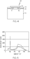
- FIG. 5 there is illustrated a Raman spectrum of 200 nm a-Si film that was e-beam sputtered coated on a borosilicate glass before and after being exposed to the above-mentioned light pulse.
- the a-Si film is annealed by the light pulse and is converted to ⁇ x-Si.
- the light pulse is needed to overcome the fact that a 200 nm a-Si coating only absorbs a portion of the emitted light.
- An identical borosilicate wafer is patterned with gold contact source/drain lines to form an eventual TFT of various widths (5-50 ⁇ m) and separations (5-50 ⁇ m). All traces are 5 mm long.
- the gold patterning is followed by an identical broadcast electron beam sputtered deposition of 200 nm of a-Si described above over the borosilicate wafer.
- the borosilicate wafer is then processed via the above-mentioned PulseForge ® 3300 system at a much lower voltage ( i.e., 550 V for 250 ⁇ s).
- the radiant power was 24 kW/cm 2 , and the radiant exposure was 5.9 J/cm 2 . Note that this level of power is below the threshold intensity described above for converting a-Si to ⁇ x-Si. Since gold is very absorbing of the light pulse, more energy is absorbed at those locations.
- the graph shows a comparison of the Raman spectrum of the thin silicon film between two different gold line pair widths (50 ⁇ m and 20 ⁇ m) and identical spacing (50 ⁇ m) between the gold traces.
- the graph shows that the space between the 50 ⁇ m traces has been converted to ⁇ x-Si, whereas the space between the 20 ⁇ m wide traces is unconverted. Similarly, the silicon film on the rest of the wafer is unconverted. This technique has converted the a-Si to ⁇ x-Si only between the gold patterned traces and nowhere else achieving automatic registration.
- a TFT device can be fabricated using a spin-on barium-strontium-titanate (BST) ceramic as the dielectric layer.
- BST spin-on barium-strontium-titanate
- This dielectric material has a relatively high dielectric constant k ( ⁇ 300), which allows a high electric field to be imparted to the field-effect channel of the TFT at low gate voltage.
- a silver gate metal is vacuum deposited onto the BST gate dielectric layer to complete the TFT.
- ⁇ x-Si is slightly n-type, a positive gate voltage should enhance the electron concentration in the channel and result in an increased drain current ( I d ).
- FIG. 7 there is illustrated a graph showing drain current ( I d ) versus drain-source voltage ( V ds ) for TFT 40 from Figure 4 .
- V g positive gate voltage
- the drain current ( I d ) is enhanced and has the saturation shape one expects for a field-effect TFT.
- the linear I-V characteristic observed at negative gate voltage indicates TFT 40 is behaving as a regular resistor when the negative gate voltage is applied. Reasons for this are unknown at this time but may be due to hole injection from the source and drain contacts. This effect, if present, is normally reduced/eliminated by suitably doping the contact regions in order to "block" hole injection.
- a-Si thin film with laterally positioned metal source-drain contacts can be "sub-threshold" annealed to a microcrystalline state within the region between the source-drain contacts.
- This has great benefit for the microelectronics industry since micro (and nano)-crystalline silicon films have high carrier mobility and other desirable features that enhance the performance of thin film devices.
- one can convert only the a-Si in the region between source/drain contacts, leaving the surrounding regions of the a-Si to remain in a high-resistance amorphous state, and thus not require patterning or otherwise isolation to limit such deleterious effects as parasitic capacitances which limit device speed and increase power dissipation.
- the present invention provides a method for thermally processing thin films on low-temperature substrates.
- the method of the present invention according to the claims also enables a TFT to be manufactured in a top gate configuration (i.e., gate on top) with minimal registration.
- Two absorbing traces form a source and drain of a TFT.
- the thin film material is preferentially thermally processed between the two absorbing ceramic traces.
- the method of the present invention has the effect of selectively curing the thin film material without the need to precisely deposit the material in the channel of the TFT.
Claims (7)
- Procédé de traitement thermique d'un film mince, ledit procédé comprenant les étapes consistant à :former deux traces absorbant la lumière sur une partie supérieure d'un film mince, les deux traces absorbantes étant constituées de céramique qui absorbe plus un rayonnement pulsé que ledit film mince, dans lequel ledit film mince est situé sur une partie supérieure d'un substrat ;irradier lesdites deux traces absorbantes à l'aide d'au moins une impulsion électromagnétique d'une source lumineuse pour chauffer lesdites deux traces absorbantes ; etpermettre à la chaleur provenant desdites deux traces absorbantes de traiter thermiquement ledit film mince.
- Procédé selon la revendication 1, dans lequel ledit substrat a une température de travail maximale inférieure à 450 °C.
- Procédé selon la revendication 1, dans lequel ledit procédé comprend en outre la fourniture d'une couche d'étalement de chaleur entre ledit film mince et ledit substrat, dans lequel la conductivité thermique de la couche d'étalement de chaleur est supérieure à celle du substrat.
- Procédé selon la revendication 1, dans lequel ladite impulsion électromagnétique est fournie par une lampe éclair.
- Procédé selon la revendication 1, dans lequel ladite impulsion électromagnétique est fournie par un arc plasma dirigé.
- Procédé selon la revendication 1, dans lequel les deux traces absorbantes sont espacées l'une de l'autre.
- Procédé selon la revendication 1, dans lequel la distance entre deux traces absorbantes est inférieure à 100 microns.
Applications Claiming Priority (2)
| Application Number | Priority Date | Filing Date | Title |
|---|---|---|---|
| US35076510P | 2010-06-02 | 2010-06-02 | |
| PCT/US2011/038937 WO2011153357A1 (fr) | 2010-06-02 | 2011-06-02 | Procédé de traitement thermique latéral de films minces sur des substrats à basse température |
Publications (3)
| Publication Number | Publication Date |
|---|---|
| EP2576860A1 EP2576860A1 (fr) | 2013-04-10 |
| EP2576860A4 EP2576860A4 (fr) | 2015-04-08 |
| EP2576860B1 true EP2576860B1 (fr) | 2017-08-09 |
Family
ID=45064782
Family Applications (1)
| Application Number | Title | Priority Date | Filing Date |
|---|---|---|---|
| EP11790412.8A Not-in-force EP2576860B1 (fr) | 2010-06-02 | 2011-06-02 | Procédé de traitement thermique latéral de films minces sur des substrats à basse température |
Country Status (7)
| Country | Link |
|---|---|
| US (3) | US8557642B2 (fr) |
| EP (1) | EP2576860B1 (fr) |
| JP (4) | JP5780682B2 (fr) |
| KR (2) | KR101648101B1 (fr) |
| CN (2) | CN103038389B (fr) |
| CA (1) | CA2801900C (fr) |
| WO (1) | WO2011153357A1 (fr) |
Families Citing this family (13)
| Publication number | Priority date | Publication date | Assignee | Title |
|---|---|---|---|---|
| US10000411B2 (en) | 2010-01-16 | 2018-06-19 | Cardinal Cg Company | Insulating glass unit transparent conductivity and low emissivity coating technology |
| US9862640B2 (en) | 2010-01-16 | 2018-01-09 | Cardinal Cg Company | Tin oxide overcoat indium tin oxide coatings, coated glazings, and production methods |
| US10000965B2 (en) | 2010-01-16 | 2018-06-19 | Cardinal Cg Company | Insulating glass unit transparent conductive coating technology |
| US10060180B2 (en) | 2010-01-16 | 2018-08-28 | Cardinal Cg Company | Flash-treated indium tin oxide coatings, production methods, and insulating glass unit transparent conductive coating technology |
| US11155493B2 (en) | 2010-01-16 | 2021-10-26 | Cardinal Cg Company | Alloy oxide overcoat indium tin oxide coatings, coated glazings, and production methods |
| US9639001B2 (en) * | 2014-02-04 | 2017-05-02 | Raytheon Company | Optically transitioned metal-insulator surface |
| US9728668B2 (en) | 2014-02-04 | 2017-08-08 | Raytheon Company | Integrated photosensitive film and thin LED display |
| US10593821B2 (en) | 2014-09-12 | 2020-03-17 | Board Of Regents, The University Of Texas System | Photonic curing of nanocrystal films for photovoltaics |
| JP7118463B2 (ja) * | 2018-01-19 | 2022-08-16 | エヌシーシー ナノ, エルエルシー | 熱的に脆弱な基板上ではんだペーストを硬化させるための方法 |
| US11028012B2 (en) | 2018-10-31 | 2021-06-08 | Cardinal Cg Company | Low solar heat gain coatings, laminated glass assemblies, and methods of producing same |
| JP7203417B2 (ja) * | 2019-01-31 | 2023-01-13 | 株式会社ブイ・テクノロジー | レーザアニール方法、レーザアニール装置、およびtft基板 |
| EP3928966A1 (fr) | 2020-06-26 | 2021-12-29 | Carl Zeiss Vision International GmbH | Procédé de fabrication d'une lentille revêtue |
| TW202236550A (zh) * | 2020-11-25 | 2022-09-16 | 美商應用材料股份有限公司 | 用於低溫處理的補充能量 |
Family Cites Families (25)
| Publication number | Priority date | Publication date | Assignee | Title |
|---|---|---|---|---|
| US5302230A (en) * | 1980-02-27 | 1994-04-12 | Ricoh Company, Ltd. | Heat treatment by light irradiation |
| EP0169485B1 (fr) * | 1984-07-17 | 1991-12-04 | Nec Corporation | Méthode et appareil pour amorcer les réactions photochimiques |
| JPH0715881B2 (ja) * | 1984-12-20 | 1995-02-22 | ソニー株式会社 | 半導体薄膜の熱処理方法 |
| JPH0727198B2 (ja) * | 1987-02-18 | 1995-03-29 | キヤノン株式会社 | 多層膜反射型マスク |
| JPH02275641A (ja) * | 1989-04-17 | 1990-11-09 | Seiko Epson Corp | 半導体装置の製造方法 |
| US5180226A (en) * | 1991-10-30 | 1993-01-19 | Texas Instruments Incorporated | Method and apparatus for precise temperature measurement |
| CA2137632A1 (fr) * | 1993-12-17 | 1995-06-18 | Douglas S. Dunn | Methode d'imagerie ablative utilisant une lampe-eclair |
| JPH09116158A (ja) * | 1995-10-17 | 1997-05-02 | Hitachi Ltd | 軽量基板薄膜半導体装置および液晶表示装置 |
| US5950078A (en) * | 1997-09-19 | 1999-09-07 | Sharp Laboratories Of America, Inc. | Rapid thermal annealing with absorptive layers for thin film transistors on transparent substrates |
| US6159832A (en) * | 1998-03-18 | 2000-12-12 | Mayer; Frederick J. | Precision laser metallization |
| JP3586558B2 (ja) * | 1998-04-17 | 2004-11-10 | 日本電気株式会社 | 薄膜の改質方法及びその実施に使用する装置 |
| TW457553B (en) * | 1999-01-08 | 2001-10-01 | Sony Corp | Process for producing thin film semiconductor device and laser irradiation apparatus |
| JP3980466B2 (ja) * | 2001-11-09 | 2007-09-26 | 株式会社半導体エネルギー研究所 | レーザー装置及びレーザー照射方法 |
| US7364952B2 (en) * | 2003-09-16 | 2008-04-29 | The Trustees Of Columbia University In The City Of New York | Systems and methods for processing thin films |
| JP2005150608A (ja) * | 2003-11-19 | 2005-06-09 | Seiko Epson Corp | ガラス基板の光処理方法およびデバイス |
| TW200541079A (en) * | 2004-06-04 | 2005-12-16 | Adv Lcd Tech Dev Ct Co Ltd | Crystallizing method, thin-film transistor manufacturing method, thin-film transistor, and display device |
| JP2006066902A (ja) * | 2004-07-28 | 2006-03-09 | Advanced Lcd Technologies Development Center Co Ltd | 半導体装置の製造方法 |
| US20070037346A1 (en) * | 2005-02-22 | 2007-02-15 | Grant Robert W | Rapid thermal annealing of targeted thin film layers |
| US7943447B2 (en) * | 2007-08-08 | 2011-05-17 | Ramesh Kakkad | Methods of fabricating crystalline silicon, thin film transistors, and solar cells |
| JP5447909B2 (ja) * | 2008-04-25 | 2014-03-19 | 株式会社日本製鋼所 | 薄膜材料の結晶化方法及びその装置 |
| US8410712B2 (en) * | 2008-07-09 | 2013-04-02 | Ncc Nano, Llc | Method and apparatus for curing thin films on low-temperature substrates at high speeds |
| JP5167050B2 (ja) * | 2008-09-30 | 2013-03-21 | ルネサスエレクトロニクス株式会社 | 半導体装置の製造方法およびマスクの製造方法 |
| US20100170566A1 (en) * | 2009-01-06 | 2010-07-08 | Arthur Don Harmala | Apparatus and method for manufacturing polymer solar cells |
| JP2010219207A (ja) * | 2009-03-16 | 2010-09-30 | Sony Corp | 金属−絶縁体相転移材料を用いた機能要素の形成方法及びこれによって形成された機能要素、並びに機能デバイスの製造方法及びこれによって製造された機能デバイス |
| JP7027198B2 (ja) | 2018-03-06 | 2022-03-01 | 株式会社Screenホールディングス | 基板処理装置 |
-
2011
- 2011-06-02 CN CN201180037944.0A patent/CN103038389B/zh active Active
- 2011-06-02 EP EP11790412.8A patent/EP2576860B1/fr not_active Not-in-force
- 2011-06-02 JP JP2013514223A patent/JP5780682B2/ja active Active
- 2011-06-02 WO PCT/US2011/038937 patent/WO2011153357A1/fr active Application Filing
- 2011-06-02 US US13/152,065 patent/US8557642B2/en active Active
- 2011-06-02 KR KR1020127034243A patent/KR101648101B1/ko active IP Right Grant
- 2011-06-02 CN CN201510261174.8A patent/CN104992901B/zh active Active
- 2011-06-02 KR KR1020157035388A patent/KR101655879B1/ko active IP Right Grant
- 2011-06-02 CA CA2801900A patent/CA2801900C/fr active Active
-
2013
- 2013-09-11 US US14/024,243 patent/US9006047B2/en active Active
-
2015
- 2015-03-02 US US14/635,729 patent/US10553450B2/en active Active
- 2015-05-26 JP JP2015106595A patent/JP6359484B2/ja active Active
-
2016
- 2016-08-10 JP JP2016157478A patent/JP2016195285A/ja not_active Withdrawn
-
2018
- 2018-12-25 JP JP2018241034A patent/JP2019071453A/ja active Pending
Non-Patent Citations (1)
| Title |
|---|
| None * |
Also Published As
| Publication number | Publication date |
|---|---|
| CA2801900C (fr) | 2018-03-13 |
| US20150311092A1 (en) | 2015-10-29 |
| CN104992901B (zh) | 2017-03-15 |
| JP2019071453A (ja) | 2019-05-09 |
| JP2014505348A (ja) | 2014-02-27 |
| JP5780682B2 (ja) | 2015-09-16 |
| US9006047B2 (en) | 2015-04-14 |
| CN103038389A (zh) | 2013-04-10 |
| KR101655879B1 (ko) | 2016-09-08 |
| US8557642B2 (en) | 2013-10-15 |
| KR20130086547A (ko) | 2013-08-02 |
| WO2011153357A1 (fr) | 2011-12-08 |
| JP6359484B2 (ja) | 2018-07-18 |
| US10553450B2 (en) | 2020-02-04 |
| JP2016195285A (ja) | 2016-11-17 |
| JP2015149513A (ja) | 2015-08-20 |
| KR20160003297A (ko) | 2016-01-08 |
| EP2576860A1 (fr) | 2013-04-10 |
| US20140017857A1 (en) | 2014-01-16 |
| KR101648101B1 (ko) | 2016-08-16 |
| CA2801900A1 (fr) | 2011-12-08 |
| US20110300676A1 (en) | 2011-12-08 |
| EP2576860A4 (fr) | 2015-04-08 |
| CN103038389B (zh) | 2015-06-17 |
| CN104992901A (zh) | 2015-10-21 |
Similar Documents
| Publication | Publication Date | Title |
|---|---|---|
| EP2576860B1 (fr) | Procédé de traitement thermique latéral de films minces sur des substrats à basse température | |
| WO2006094231A1 (fr) | Systeme et procede pour l'etablissement de materiau conducteur sur un substrat | |
| JP2015149513A5 (fr) | ||
| Yoo et al. | Sub-second photo-annealing of solution-processed metal oxide thin-film transistors via irradiation of intensely pulsed white light | |
| Fiory | Recent developments in rapid thermal processing | |
| Li et al. | Precise Patterning of Large‐Scale TFT Arrays Based on Solution‐Processed Oxide Semiconductors: A Comparative Study of Additive and Subtractive Approaches | |
| JP2012178439A (ja) | 半導体デバイス及びその製造方法 | |
| Trifunovic et al. | Solution-based polycrystalline silicon transistors produced on a paper substrate | |
| Weidling et al. | Large-area photonic lift-off process for flexible thin-film transistors | |
| TWI677921B (zh) | 基於在沉積的非晶半導體材料基礎上形成結晶半導體材料的技術及相關的半導體裝置 | |
| WO2006098513A1 (fr) | Procédé de traitement thermique et procédé de cristallisation de semi-conducteur | |
| Thompson et al. | Millisecond microwave annealing: Driving microelectronics nano | |
| Noh et al. | Pulse thermal processing for low thermal budget integration of IGZO thin film transistors | |
| US20040058501A1 (en) | Apparatus and method for adiabatically heating a semiconductor surface | |
| Hernandez et al. | Laser thermal processing using an optical coating for ultra shallow junction formation | |
| Balestra | Silicon‐On‐Insulator Devices | |
| Jung et al. | Enhancement of electrical properties of a-IGZO thin film transistor by low temperature (150° C) microwave annealing for flexible electronics | |
| Hishitani et al. | Solution-derived SiO2 gate insulator formed by CO2 laser annealing for polycrystalline silicon thin-film transistors | |
| TWI587422B (zh) | 晶圓微波退火之晶圓承載結構及其應用 | |
| Coutanson et al. | Mechanisms and application of the Excimer laser doping from spin-on glass sources for USJ fabrication | |
| Biasotto | DotFETs: MOSFETs Strained by a Single SiGe Dot in a Low-temperature ELA Technology | |
| ELLION et al. | Time-resolved analysis of flash-assist RTP thermal pulse progression in SOI and bulk silicon wafers | |
| Wang et al. | Instability Effect on CLC nTFTs with Positive-Bias Temperature Stress |
Legal Events
| Date | Code | Title | Description |
|---|---|---|---|
| PUAI | Public reference made under article 153(3) epc to a published international application that has entered the european phase |
Free format text: ORIGINAL CODE: 0009012 |
|
| 17P | Request for examination filed |
Effective date: 20121227 |
|
| AK | Designated contracting states |
Kind code of ref document: A1 Designated state(s): AL AT BE BG CH CY CZ DE DK EE ES FI FR GB GR HR HU IE IS IT LI LT LU LV MC MK MT NL NO PL PT RO RS SE SI SK SM TR |
|
| DAX | Request for extension of the european patent (deleted) | ||
| RA4 | Supplementary search report drawn up and despatched (corrected) |
Effective date: 20150305 |
|
| RIC1 | Information provided on ipc code assigned before grant |
Ipc: B29C 35/08 20060101ALI20150227BHEP Ipc: C23C 16/56 20060101AFI20150227BHEP Ipc: B29C 35/02 20060101ALI20150227BHEP Ipc: H01L 29/786 20060101ALI20150227BHEP Ipc: H01L 21/02 20060101ALI20150227BHEP Ipc: H01L 29/66 20060101ALI20150227BHEP Ipc: H01L 27/12 20060101ALI20150227BHEP Ipc: H01L 21/20 20060101ALI20150227BHEP |
|
| 17Q | First examination report despatched |
Effective date: 20151215 |
|
| GRAP | Despatch of communication of intention to grant a patent |
Free format text: ORIGINAL CODE: EPIDOSNIGR1 |
|
| INTG | Intention to grant announced |
Effective date: 20170217 |
|
| GRAS | Grant fee paid |
Free format text: ORIGINAL CODE: EPIDOSNIGR3 |
|
| GRAA | (expected) grant |
Free format text: ORIGINAL CODE: 0009210 |
|
| AK | Designated contracting states |
Kind code of ref document: B1 Designated state(s): AL AT BE BG CH CY CZ DE DK EE ES FI FR GB GR HR HU IE IS IT LI LT LU LV MC MK MT NL NO PL PT RO RS SE SI SK SM TR |
|
| REG | Reference to a national code |
Ref country code: GB Ref legal event code: FG4D |
|
| REG | Reference to a national code |
Ref country code: CH Ref legal event code: EP Ref country code: AT Ref legal event code: REF Ref document number: 916941 Country of ref document: AT Kind code of ref document: T Effective date: 20170815 |
|
| REG | Reference to a national code |
Ref country code: IE Ref legal event code: FG4D |
|
| REG | Reference to a national code |
Ref country code: DE Ref legal event code: R096 Ref document number: 602011040456 Country of ref document: DE |
|
| REG | Reference to a national code |
Ref country code: NL Ref legal event code: MP Effective date: 20170809 |
|
| REG | Reference to a national code |
Ref country code: LT Ref legal event code: MG4D |
|
| REG | Reference to a national code |
Ref country code: AT Ref legal event code: MK05 Ref document number: 916941 Country of ref document: AT Kind code of ref document: T Effective date: 20170809 |
|
| PG25 | Lapsed in a contracting state [announced via postgrant information from national office to epo] |
Ref country code: FI Free format text: LAPSE BECAUSE OF FAILURE TO SUBMIT A TRANSLATION OF THE DESCRIPTION OR TO PAY THE FEE WITHIN THE PRESCRIBED TIME-LIMIT Effective date: 20170809 Ref country code: NL Free format text: LAPSE BECAUSE OF FAILURE TO SUBMIT A TRANSLATION OF THE DESCRIPTION OR TO PAY THE FEE WITHIN THE PRESCRIBED TIME-LIMIT Effective date: 20170809 Ref country code: HR Free format text: LAPSE BECAUSE OF FAILURE TO SUBMIT A TRANSLATION OF THE DESCRIPTION OR TO PAY THE FEE WITHIN THE PRESCRIBED TIME-LIMIT Effective date: 20170809 Ref country code: SE Free format text: LAPSE BECAUSE OF FAILURE TO SUBMIT A TRANSLATION OF THE DESCRIPTION OR TO PAY THE FEE WITHIN THE PRESCRIBED TIME-LIMIT Effective date: 20170809 Ref country code: NO Free format text: LAPSE BECAUSE OF FAILURE TO SUBMIT A TRANSLATION OF THE DESCRIPTION OR TO PAY THE FEE WITHIN THE PRESCRIBED TIME-LIMIT Effective date: 20171109 Ref country code: LT Free format text: LAPSE BECAUSE OF FAILURE TO SUBMIT A TRANSLATION OF THE DESCRIPTION OR TO PAY THE FEE WITHIN THE PRESCRIBED TIME-LIMIT Effective date: 20170809 Ref country code: AT Free format text: LAPSE BECAUSE OF FAILURE TO SUBMIT A TRANSLATION OF THE DESCRIPTION OR TO PAY THE FEE WITHIN THE PRESCRIBED TIME-LIMIT Effective date: 20170809 |
|
| PG25 | Lapsed in a contracting state [announced via postgrant information from national office to epo] |
Ref country code: ES Free format text: LAPSE BECAUSE OF FAILURE TO SUBMIT A TRANSLATION OF THE DESCRIPTION OR TO PAY THE FEE WITHIN THE PRESCRIBED TIME-LIMIT Effective date: 20170809 Ref country code: GR Free format text: LAPSE BECAUSE OF FAILURE TO SUBMIT A TRANSLATION OF THE DESCRIPTION OR TO PAY THE FEE WITHIN THE PRESCRIBED TIME-LIMIT Effective date: 20171110 Ref country code: RS Free format text: LAPSE BECAUSE OF FAILURE TO SUBMIT A TRANSLATION OF THE DESCRIPTION OR TO PAY THE FEE WITHIN THE PRESCRIBED TIME-LIMIT Effective date: 20170809 Ref country code: PL Free format text: LAPSE BECAUSE OF FAILURE TO SUBMIT A TRANSLATION OF THE DESCRIPTION OR TO PAY THE FEE WITHIN THE PRESCRIBED TIME-LIMIT Effective date: 20170809 Ref country code: IS Free format text: LAPSE BECAUSE OF FAILURE TO SUBMIT A TRANSLATION OF THE DESCRIPTION OR TO PAY THE FEE WITHIN THE PRESCRIBED TIME-LIMIT Effective date: 20171209 Ref country code: BG Free format text: LAPSE BECAUSE OF FAILURE TO SUBMIT A TRANSLATION OF THE DESCRIPTION OR TO PAY THE FEE WITHIN THE PRESCRIBED TIME-LIMIT Effective date: 20171109 Ref country code: LV Free format text: LAPSE BECAUSE OF FAILURE TO SUBMIT A TRANSLATION OF THE DESCRIPTION OR TO PAY THE FEE WITHIN THE PRESCRIBED TIME-LIMIT Effective date: 20170809 |
|
| PG25 | Lapsed in a contracting state [announced via postgrant information from national office to epo] |
Ref country code: RO Free format text: LAPSE BECAUSE OF FAILURE TO SUBMIT A TRANSLATION OF THE DESCRIPTION OR TO PAY THE FEE WITHIN THE PRESCRIBED TIME-LIMIT Effective date: 20170809 Ref country code: CZ Free format text: LAPSE BECAUSE OF FAILURE TO SUBMIT A TRANSLATION OF THE DESCRIPTION OR TO PAY THE FEE WITHIN THE PRESCRIBED TIME-LIMIT Effective date: 20170809 Ref country code: DK Free format text: LAPSE BECAUSE OF FAILURE TO SUBMIT A TRANSLATION OF THE DESCRIPTION OR TO PAY THE FEE WITHIN THE PRESCRIBED TIME-LIMIT Effective date: 20170809 |
|
| REG | Reference to a national code |
Ref country code: DE Ref legal event code: R097 Ref document number: 602011040456 Country of ref document: DE |
|
| PG25 | Lapsed in a contracting state [announced via postgrant information from national office to epo] |
Ref country code: EE Free format text: LAPSE BECAUSE OF FAILURE TO SUBMIT A TRANSLATION OF THE DESCRIPTION OR TO PAY THE FEE WITHIN THE PRESCRIBED TIME-LIMIT Effective date: 20170809 Ref country code: SK Free format text: LAPSE BECAUSE OF FAILURE TO SUBMIT A TRANSLATION OF THE DESCRIPTION OR TO PAY THE FEE WITHIN THE PRESCRIBED TIME-LIMIT Effective date: 20170809 Ref country code: IT Free format text: LAPSE BECAUSE OF FAILURE TO SUBMIT A TRANSLATION OF THE DESCRIPTION OR TO PAY THE FEE WITHIN THE PRESCRIBED TIME-LIMIT Effective date: 20170809 Ref country code: SM Free format text: LAPSE BECAUSE OF FAILURE TO SUBMIT A TRANSLATION OF THE DESCRIPTION OR TO PAY THE FEE WITHIN THE PRESCRIBED TIME-LIMIT Effective date: 20170809 |
|
| PLBE | No opposition filed within time limit |
Free format text: ORIGINAL CODE: 0009261 |
|
| STAA | Information on the status of an ep patent application or granted ep patent |
Free format text: STATUS: NO OPPOSITION FILED WITHIN TIME LIMIT |
|
| 26N | No opposition filed |
Effective date: 20180511 |
|
| PG25 | Lapsed in a contracting state [announced via postgrant information from national office to epo] |
Ref country code: SI Free format text: LAPSE BECAUSE OF FAILURE TO SUBMIT A TRANSLATION OF THE DESCRIPTION OR TO PAY THE FEE WITHIN THE PRESCRIBED TIME-LIMIT Effective date: 20170809 |
|
| REG | Reference to a national code |
Ref country code: DE Ref legal event code: R119 Ref document number: 602011040456 Country of ref document: DE |
|
| REG | Reference to a national code |
Ref country code: CH Ref legal event code: PL |
|
| GBPC | Gb: european patent ceased through non-payment of renewal fee |
Effective date: 20180602 |
|
| REG | Reference to a national code |
Ref country code: BE Ref legal event code: MM Effective date: 20180630 |
|
| REG | Reference to a national code |
Ref country code: IE Ref legal event code: MM4A |
|
| PG25 | Lapsed in a contracting state [announced via postgrant information from national office to epo] |
Ref country code: MC Free format text: LAPSE BECAUSE OF FAILURE TO SUBMIT A TRANSLATION OF THE DESCRIPTION OR TO PAY THE FEE WITHIN THE PRESCRIBED TIME-LIMIT Effective date: 20170809 Ref country code: LU Free format text: LAPSE BECAUSE OF NON-PAYMENT OF DUE FEES Effective date: 20180602 |
|
| PG25 | Lapsed in a contracting state [announced via postgrant information from national office to epo] |
Ref country code: CH Free format text: LAPSE BECAUSE OF NON-PAYMENT OF DUE FEES Effective date: 20180630 Ref country code: DE Free format text: LAPSE BECAUSE OF NON-PAYMENT OF DUE FEES Effective date: 20190101 Ref country code: GB Free format text: LAPSE BECAUSE OF NON-PAYMENT OF DUE FEES Effective date: 20180602 Ref country code: IE Free format text: LAPSE BECAUSE OF NON-PAYMENT OF DUE FEES Effective date: 20180602 Ref country code: LI Free format text: LAPSE BECAUSE OF NON-PAYMENT OF DUE FEES Effective date: 20180630 Ref country code: FR Free format text: LAPSE BECAUSE OF NON-PAYMENT OF DUE FEES Effective date: 20180630 |
|
| PG25 | Lapsed in a contracting state [announced via postgrant information from national office to epo] |
Ref country code: BE Free format text: LAPSE BECAUSE OF NON-PAYMENT OF DUE FEES Effective date: 20180630 |
|
| PG25 | Lapsed in a contracting state [announced via postgrant information from national office to epo] |
Ref country code: MT Free format text: LAPSE BECAUSE OF NON-PAYMENT OF DUE FEES Effective date: 20180602 |
|
| PG25 | Lapsed in a contracting state [announced via postgrant information from national office to epo] |
Ref country code: TR Free format text: LAPSE BECAUSE OF FAILURE TO SUBMIT A TRANSLATION OF THE DESCRIPTION OR TO PAY THE FEE WITHIN THE PRESCRIBED TIME-LIMIT Effective date: 20170809 |
|
| PG25 | Lapsed in a contracting state [announced via postgrant information from national office to epo] |
Ref country code: HU Free format text: LAPSE BECAUSE OF FAILURE TO SUBMIT A TRANSLATION OF THE DESCRIPTION OR TO PAY THE FEE WITHIN THE PRESCRIBED TIME-LIMIT; INVALID AB INITIO Effective date: 20110602 Ref country code: PT Free format text: LAPSE BECAUSE OF FAILURE TO SUBMIT A TRANSLATION OF THE DESCRIPTION OR TO PAY THE FEE WITHIN THE PRESCRIBED TIME-LIMIT Effective date: 20170809 |
|
| PG25 | Lapsed in a contracting state [announced via postgrant information from national office to epo] |
Ref country code: MK Free format text: LAPSE BECAUSE OF NON-PAYMENT OF DUE FEES Effective date: 20170809 Ref country code: CY Free format text: LAPSE BECAUSE OF FAILURE TO SUBMIT A TRANSLATION OF THE DESCRIPTION OR TO PAY THE FEE WITHIN THE PRESCRIBED TIME-LIMIT Effective date: 20170809 |
|
| PG25 | Lapsed in a contracting state [announced via postgrant information from national office to epo] |
Ref country code: AL Free format text: LAPSE BECAUSE OF FAILURE TO SUBMIT A TRANSLATION OF THE DESCRIPTION OR TO PAY THE FEE WITHIN THE PRESCRIBED TIME-LIMIT Effective date: 20170809 |