EP2573771A2 - System und Verfahren zum Kontrollieren des Keilabstands in einem Speichergerät - Google Patents
System und Verfahren zum Kontrollieren des Keilabstands in einem Speichergerät Download PDFInfo
- Publication number
- EP2573771A2 EP2573771A2 EP12178169A EP12178169A EP2573771A2 EP 2573771 A2 EP2573771 A2 EP 2573771A2 EP 12178169 A EP12178169 A EP 12178169A EP 12178169 A EP12178169 A EP 12178169A EP 2573771 A2 EP2573771 A2 EP 2573771A2
- Authority
- EP
- European Patent Office
- Prior art keywords
- clock
- data
- phase
- domain
- circuit
- Prior art date
- Legal status (The legal status is an assumption and is not a legal conclusion. Google has not performed a legal analysis and makes no representation as to the accuracy of the status listed.)
- Withdrawn
Links
Images



Classifications
-
- G—PHYSICS
- G11—INFORMATION STORAGE
- G11B—INFORMATION STORAGE BASED ON RELATIVE MOVEMENT BETWEEN RECORD CARRIER AND TRANSDUCER
- G11B20/00—Signal processing not specific to the method of recording or reproducing; Circuits therefor
- G11B20/10—Digital recording or reproducing
- G11B20/14—Digital recording or reproducing using self-clocking codes
- G11B20/1403—Digital recording or reproducing using self-clocking codes characterised by the use of two levels
-
- G—PHYSICS
- G11—INFORMATION STORAGE
- G11B—INFORMATION STORAGE BASED ON RELATIVE MOVEMENT BETWEEN RECORD CARRIER AND TRANSDUCER
- G11B5/00—Recording by magnetisation or demagnetisation of a record carrier; Reproducing by magnetic means; Record carriers therefor
- G11B5/02—Recording, reproducing, or erasing methods; Read, write or erase circuits therefor
-
- G—PHYSICS
- G11—INFORMATION STORAGE
- G11B—INFORMATION STORAGE BASED ON RELATIVE MOVEMENT BETWEEN RECORD CARRIER AND TRANSDUCER
- G11B20/00—Signal processing not specific to the method of recording or reproducing; Circuits therefor
- G11B20/10—Digital recording or reproducing
- G11B20/10009—Improvement or modification of read or write signals
- G11B20/10222—Improvement or modification of read or write signals clock-related aspects, e.g. phase or frequency adjustment or bit synchronisation
-
- G—PHYSICS
- G11—INFORMATION STORAGE
- G11B—INFORMATION STORAGE BASED ON RELATIVE MOVEMENT BETWEEN RECORD CARRIER AND TRANSDUCER
- G11B5/00—Recording by magnetisation or demagnetisation of a record carrier; Reproducing by magnetic means; Record carriers therefor
- G11B5/48—Disposition or mounting of heads or head supports relative to record carriers ; arrangements of heads, e.g. for scanning the record carrier to increase the relative speed
- G11B5/58—Disposition or mounting of heads or head supports relative to record carriers ; arrangements of heads, e.g. for scanning the record carrier to increase the relative speed with provision for moving the head for the purpose of maintaining alignment of the head relative to the record carrier during transducing operation, e.g. to compensate for surface irregularities of the latter or for track following
- G11B5/596—Disposition or mounting of heads or head supports relative to record carriers ; arrangements of heads, e.g. for scanning the record carrier to increase the relative speed with provision for moving the head for the purpose of maintaining alignment of the head relative to the record carrier during transducing operation, e.g. to compensate for surface irregularities of the latter or for track following for track following on disks
- G11B5/59633—Servo formatting
- G11B5/5965—Embedded servo format
Definitions
- the present inventions are related to systems and methods for storing and accessing data to/from a storage medium.
- a typical storage device includes a magnetic storage medium storing information that is magnetically represented on the storage medium.
- a head is disposed in relation to the storage medium that senses the magnetically represented information and provides an electrical signal corresponding to the magnetically represented information. This electrical signal is ultimately passed to a data detection circuit that performs one or more data detection processes in order to recover the information originally written to the storage medium.
- the information maintained on the storage medium typically includes both user data and synchronization data.
- the user data may be considered a random pattern, while the synchronization data is generally a defined pattern that may be used to synchronize to the phase of the data on the storage medium, and to set an appropriate gain to be applied to data retrieved from the storage medium.
- synchronization data is generally a defined pattern that may be used to synchronize to the phase of the data on the storage medium, and to set an appropriate gain to be applied to data retrieved from the storage medium. It is common to utilize phase lock loops to synchronize to the synchronization data. Such an approach is generally effective, but can require a pattern of substantial length to properly process. Such pattern length wastes space on a storage medium and/or reduces transmission bandwidth.
- the present inventions are related to systems and methods for storing and accessing data to/from a storage medium.
- Various embodiments of the present invention provide clock generation systems that include, a first clock multiplier circuit, a second clock multiplier circuit, a modulus accumulator circuit, and a data clock phase control circuit.
- the first clock multiplier circuit is operable to multiply a reference clock by a first multiplier to yield a first domain clock
- the second clock multiplier circuit is operable to multiply the reference clock by a second multiplier to yield a second domain clock.
- the modulus accumulator circuit is operable to yield a value indicating a fractional amount of the second domain clock that an edge of the second domain clock is offset from a trigger signal.
- the data clock phase control circuit is operable to phase shift the second domain clock by a phase amount corresponding to the fractional amount.
- the system is implemented as part of a storage device. In some cases, such a storage device is a hard disk drive. In one or more instances of the aforementioned embodiments, the system is implemented as an integrated circuit.
- the system further includes a storage medium including a servo wedge and a user data region.
- the first domain clock corresponds to a frequency of data in the servo wedge
- the second domain clock corresponds to a frequency of data in the user data region.
- the servo wedge includes a sector address mark
- the trigger signal is asserted based at least in part on identification of the sector address mark.
- the trigger signal is asserted synchronous to the first domain clock.
- the system further comprises a rounding and scaling circuit.
- the rounding and scaling circuit is operable to modify the value indicating the fractional amount to conform to a step size implementable by the data clock phase control circuit to yield the phase amount corresponding to the fractional amount.
- the phase amount is a first phase amount
- the data clock phase control circuit is operable to phase shift the second domain clock by a second phase amount and subsequently to phase shift the second domain clock by a third phase amount. The combination of the second phase amount and the third phase amount yields the first phase amount.
- Other embodiments of the present invention provide methods for multi-domain clock generation that includes: receiving a trigger signal; based at least in part on the trigger signal, calculating a frequency error based on a difference between an expected count and an actual count; multiplying a reference clock by a first multiplier and an error percentage derived from the frequency error to yield a first domain clock; multiplying the reference clock by a second multiplier and the error percentage to yield a second domain clock; determining a fractional amount of the second domain clock that an edge of the second domain clock is offset from the trigger signal; and phase shifting the second domain clock by a phase amount corresponding to the fractional amount.
- the method further includes accessing data from a storage medium.
- the storage medium includes a servo wedge and a user data region
- the first domain clock corresponds to a frequency of data in the servo wedge
- the second domain clock corresponds to a frequency of data in the user data region.
- the trigger signal is received based upon data accessed from the servo wedge.
- the servo wedge includes a sector address mark
- the trigger signal is asserted based at least in part on identification of the sector address mark.
- the trigger signal is received synchronous to the first domain clock.
- the method further includes modifying the fractional amount to conform to a step size implementable by a data clock phase control circuit applying the phase shift to yield the phase amount corresponding to the fractional amount.
- the phase amount is a first phase amount
- a data clock phase control circuit performing the phase shift is operable to phase shift the second domain clock by a second phase amount and subsequently to phase shift the second domain clock by a third phase amount. The combination of the second phase amount and the third phase amount yields the first phase amount.
- Yet other embodiments of the present invention provide data storage devices that include: a storage medium including a servo wedge and a user data region, a read head disposed in relation to the storage medium and operable to sense information from the storage medium, and a read channel circuit.
- the read channel circuit includes: a first clock multiplier circuit, a second clock multiplier circuit, a modulus accumulator circuit, and a data clock phase control circuit.
- the first clock multiplier circuit is operable to multiply a reference clock by a first multiplier to yield a first domain clock.
- the first domain clock corresponds to a frequency of the information from the servo wedge.
- the second clock multiplier circuit is operable to multiply the reference clock by a second multiplier to yield a second domain clock.
- the second domain clock corresponds to a frequency of the information from the user data region.
- the modulus accumulator circuit is operable to yield a value indicating a fractional amount of the second domain clock that an edge of the second domain clock is offset from a trigger signal.
- the data clock phase control circuit operable to phase shift the second domain clock by a phase amount corresponding to the fractional amount.
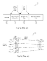
- Figs. 1a, 1b and 1c show an existing storage medium along with stored information
- Fig. 2 depicts a storage device including a read channel circuit having fractional data wedge spacing circuitry in accordance with some embodiments of the present invention
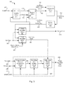
- Fig. 3 shows a fractional data wedge spacing circuit in accordance with various embodiments of the present invention
- Fig. 4 is a timing diagram showing an example operation of the fractional data wedge spacing circuit of Fig. 3 ;
- Fig. 5 is a flow diagram showing a method for fractional data wedge spacing in accordance with some embodiments of the present invention.
- the present inventions are related to systems and methods for storing and accessing data to/from a storage medium.
- Such data processing circuits may include disk lock clock circuitry operable to lock the clock used for processing data in a user data region with a clock used for processing data in a servo wedge (i.e., locking to the rotational speed of a disk medium).
- servo data sector or "servo wedge” are used in their broadest sense to mean a region of a storage medium that includes synchronization information.
- user data region is used in its broadest sense to mean a region disposed in relation to one or more servo wedges that may be written or read.
- a once per clock fractional phase alignment is performed to fractionally offset the clock used for processing data in a user data region such that the clock is at least initially placed in a known phase relationship with a clock used for processing data from a servo wedge.
- fractional phase alignment allows for a clock that is usable in both a servo clock domain and the user data clock domain even though the clock used in the servo data region and the clock used in the user data region may be arbitrarily programmed to operate at different frequencies.
- the clock architecture is designed with a knowledge of an exact fractional number of period of a data clock which are desired to fit in one servo wedge to servo wedge interval.
- servo wedge 100 may include a preamble pattern 102 which allows the system to recover the timing and gain of the written servo data.
- Preamble 102 may be used to generate a clock at a phase and frequency useful for processing data from servo wedge 100 as is known in the art.
- Preamble pattern 102 is typically followed by a servo address mark (SAM) 104 which is the same for all servo wedges.
- SAM 104 is then followed by encoded servo Gray data 106, and Gray data 106 is followed by one or more burst demodulation fields 108.
- SAM servo address mark
- Gray data 106 may represent the track number/cylinder information and provides coarse positioning information for a read head traversing a magnetic storage medium.
- Burst demodulation field 108 provides fine positioning information for the read head traversing a magnetic storage medium.
- Fig.1b the aforementioned servo wedge 100 is shown incorporated as part of data sectors 170 distributed across a number of tracks 160 that extend in a radial pattern around a magnetic storage medium 150. Sectors 170 include both servo wedges and intervening user data regions.
- a read/write head assembly traverses an individual track 160 over alternating servo wedges 100 and intervening user data regions.
- a SAMFOUND signal is generated providing an indication of the location of the read/write head assembly in relation to magnetic storage medium 150.
- the time interval from the last SAMFOUND signal is used to determine whether a disk lock clock is synchronized to the placement of servo wedges 100 on storage medium 150. Where the disk lock clock is not properly locked, it is increased or decreased by an error amount indicated by the difference between the expected timing between consecutive SAMFOUND signals and the actual timing. This clock adjustment is performed once for each servo wedge 100.
- a storage medium 190 is shown with two example tracks 160a, 160e indicated as dashed lines.
- the tracks are segregated by servo data written within wedges 101a, 101b.
- These wedges include synchronization data similar to that discussed above in relation to example servo wedge 100.
- the synchronization data is used for control and synchronization of a read/write head assembly over a desired location on storage medium 190.
- the servo data generally includes a preamble pattern 102 followed by a sector address mark 104 (SAM).
- SAM sector address mark
- Sector address mark 104 is followed by a Gray code 106
- Gray code 106 is followed by burst information 108.
- a servo data set may have two or more fields of burst information. Yet further, it should be noted that different information may be included in the servo fields such as, for example, repeatable run-out information that may appear after burst information 108. Between the wedges 101a and 101b, a user data region 171 is provided.
- storage medium 190 is rotated in relation to a sensor (e.g., a read/write head assembly (not shown)) that senses information from storage medium 190.
- a sensor e.g., a read/write head assembly (not shown)
- the sensor would sense servo data from wedge 100b (i.e., during a servo data period) followed by user data from a user data region between wedge 101b and wedge 101a (i.e., during a user data period) and then servo data from wedge 101a.
- the sensor would sense servo data from wedge 101b then write data to the user data region between wedge 101b and wedge 101a. Then, the sensor would be switched to sense a remaining portion of the user data region followed by the servo data from wedge 101a.
- Storage system 200 may be, for example, a hard disk drive.
- Storage system 200 also includes a preamplifier 291, an interface controller 285, a hard disk controller 289, a motor controller 299, a spindle motor 297, a disk platter 295, and a read/write head 293.
- Interface controller 285 controls addressing and timing of data to/from disk platter 295.
- the data on disk platter 295 consists of groups of magnetic signals that may be detected by read/write head assembly 293 when the assembly is properly positioned over disk platter 295.
- disk platter 295 includes magnetic signals recorded in accordance with either a longitudinal or a perpendicular recording scheme.
- read/write head assembly 293 is accurately positioned by motor controller 299 over a desired data track on disk platter 295.
- Motor controller 299 both positions read/write head assembly 293 in relation to disk platter 295 and drives spindle motor 297 by moving read/write head assembly to the proper data track on disk platter 295 under the direction of hard disk controller 289.
- Spindle motor 297 spins disk platter 295 at a determined spin rate (RPMs).
- RPMs spin rate
- This minute analog signal is transferred from read/write head assembly 293 to read channel circuit 287 via preamplifier 291.
- Preamplifier 291 is operable to amplify the minute analog signals accessed from disk platter 295.
- read channel circuit 287 decodes and digitizes the received analog signal to recreate the information originally written to disk platter 295.
- This data is provided as read data 283 to a receiving circuit.
- read channel circuit 287 performs a data detection and synchronization process using a data processing circuit with reduced complexity timing loops.
- Such a data processing circuit may include fractional data wedge spacing circuitry similar to that discussed below in relation to Fig. 3 , and/or may operate consistent with the method discussed below in relation to Fig. 4 .
- a write operation is substantially the opposite of the preceding read operation with write data 281 being provided to read channel circuit 287. This data is then encoded and written to disk platter 295.
- storage system 200 may be integrated into a larger storage system such as, for example, a RAID (redundant array of inexpensive disks or redundant array of independent disks) based storage system. It should also be noted that various functions or blocks of storage system 200 may be implemented in either software or firmware, while other functions or blocks are implemented in hardware.
- RAID redundant array of inexpensive disks or redundant array of independent disks
- Fractional data wedge spacing circuit 300 includes a counter circuit 311 that is incremented on each rising edge of a servo clock 313, and is reset each time a SAMFOUND signal 315 is asserted. As suggested above, SAMFOUND signal 315 is asserted whenever a servo address mark 104 is identified in a servo wedge 100. In addition, each time SAMFOUND signal 315 is asserted, a count value 314 from counter circuit 311 is stored to a register circuit 321. Register circuit 321 provides count value 314 as a count output 324 to a comparator circuit 340.
- the distance between successive assertions of SAMFOUND signal 315 is known and may be expressed as a number of clock cycles. This known number of clock cycles is referred to as an expected SAM to SAM count 303.
- Expected SAM to SAM count 303 is provided to comparator circuit 340 that is operable to determine a difference between expected SAM to SAM count 303 and count output 324, and to provide the difference as frequency error 351. Said another way, any difference between expected SAM to SAM count 303 and the actual number of clock cycles between successive assertions of SAMFOUND signal 315 is due to a frequency error.
- Reference clock 363 is phase and frequency aligned with a clock generated using information from servo wedges.
- the servo clock multiplier is a defined multiple of the frequency of reference clock 363 to yield servo clock 313. In some cases, the servo clock multiplier may be variable through programming or may be fixed.
- the servo clock multiplier is thirty-four (34) (i.e., 1.02GHz/30MHz). It should be noted that the servo clock multiplier does not need to be an integer value, but may include a fractional component as well. Where fractional values are included, the size of the registers in clock multiplier circuit 361 are increased to accommodate the bits representing the fractional portion.
- a clock multiplier circuit 381 multiplies reference clock 363 by a value corresponding to frequency error percentage 359 and by a data to servo clock ratio 304 to yield a raw data clock 383.
- Raw Data Clock 383 Data Clock Multiplier * Reference Clock 363 * 1 + Frequency Error Percentage 359 * Data to Servo Clock Ratio 304
- the data clock multiplier is a defined multiple of the frequency of reference clock 363 to yield raw data clock 383.
- the data clock multiplier is forty-six (46) (i.e., 1.38GHz/30MHz).
- the data clock multiplier does not need to be an integer value, but may include a fractional component as well. Where fractional values are included, the size of the registers in clock multiplier circuit 381 are increased to accommodate the bits representing the fractional portion.
- Such disk clock locking locks the frequency of raw data clock 383 to a frequency proportional to the frequency of servo clock 313.
- Such frequency association between an internal read channel clock and the spinning disk so that among other things user data regions extending between successive servo wedges are written with less frequency variation. This reduction in frequency variation reduces the amount of range that a timing recovery loop circuit governing user data writing must operate.
- the previously described portion of data wedge spacing circuit 300 provides servo clock 313 corresponding to the frequency of information in the servo wedges and raw data clock 383 corresponding to the frequency of data stored to user data regions intervening between successive servo wedges.
- Both servo clock 313 and raw data clock 383 are derived from the same reference clock 363 and are adjusted by the same frequency error percentage 359.
- raw data clock 383 and servo clock 313 can run at different frequencies even if a phase lock is achieved for the servo wedges, raw data clock 383 may still drift in phase over time as it beats against servo clock 313 from one revolution of the disk to the next revolution of the disk.
- fractional data wedge spacing circuit 300 is operable to achieve phase lock at a defined point in both the domain of servo clock 313 and raw data clock 383 even though the two clocks may be programmed to have arbitrarily different frequencies.
- a predicted and controlled phase adjustment is made to raw data clock 383 once per servo wedge that is not based on the timing recovery loop read back waveform, but rather on the system knowledge of the frequency ratio between raw data clock 383 and servo clock 313.
- phase adjustment circuit 301 assures that the first edge of a phase adjusted data clock 399 is phase aligned with a corresponding edge of servo clock 313.
- Phase adjustment circuit 301 is operable to apply a fractional phase offset (i.e., sub-period of servo clock 313) to raw data clock 383 and thereby align phase adjusted data clock 399 with servo clock 313.
- raw data clock 383 is frequency matched to servo clock 313 by clock multiplier circuit 381 (i.e., matched to a frequency proportional to that of servo clock 313).
- phase adjusted data clock 399 is both phase and frequency aligned at the end of a servo wedge and the beginning of a user data region.
- Phase adjustment circuit 301 includes a programmable modulus accumulator circuit 389 that receives numerator value 385 and denominator value 386.
- Denominator value 386 is set equal to the servo clock multiplier used by multiplier circuit 361.
- Programmable modulus accumulator circuit 389 calculates the number of periods of raw data clock 383 mod denominator value 386 to yield a modulus output 391. Thus, for example, where the denominator value is eight and the count of the number of raw data clock 383 periods is nine, modulus output is one plus one eighth. Modulus output 391 is updated each time SAMFOUND 315 is asserted.
- programmable modulus accumulator circuit 389 operates in accordance with the following pseudo-code:
- modulus output 391 is updated upon assertion of SAMFOUND signal 315.
- Modulus output 391 is provided to a rounding and scaling circuit 393 that rounds to modulus output to a step size that is achievable by a data clock phase control circuit 397.
- Rounding and scaling circuit 393 provides the modified modulus output 391 as a modified output 395.
- Data clock phase control circuit 397 applies a phase shift to raw data clock 383 that corresponds to modified output 395 to yield a phase adjusted data clock 399.
- Data clock phase control circuit 397 may be any circuit known in the art that is capable of applying a phase shift to a clock signal to yield a phase shifted clock signal as an output.
- phase shift circuits that may be used in relation to different embodiments of the present invention.
- SAMFOUND signal 315 is synchronous to servo clock 313
- the first rising edge of phase adjusted data clock 399 after assertion of SAMFOUND signal 315 is phase aligned with servo clock 313.
- the phase alignment is exact, while in other cases there is a known delay between the rising edge of servo clock 313 and phase adjusted data clock 399 which, because it is known, can be compensated.
- a trigger other than SAMFOUND signal 315 that is also synchronized to servo clock 313 may be used. In either case, the initial edge of phase adjusted data clock 399 after assertion of the trigger is forced into a defined phase alignment with servo clock 397 by data clock phase control signal 397.
- an ability to control the phase of raw data clock 383 may allow for improved format efficiency (reduced amount of formatting bits) by eliminating some uncertainty in the relative position of the servo wedges and intervening data regions.
- a benefit to shingled recording applications may be achieved if the clock phase for adjacent data tracks is always known and controlled.
- servo clock multiplier is thirty-four (34) and data clock multiplier is forty-six (46).
- Clock multiplier circuit 361 and clock multiplier circuit 381 are used to lock the phase and frequency of servo clock 313 to force exactly 10,000 periods of servo clock 313 per SAM to SAM period (i.e., expected SAM to SAM count 303 is 10,000).
- This disk lock forces the interval in order to avoid phase drift of raw data clock 383 relative to the servo wedges on either side of a user data region.
- phase adjusted data clock 399 a data processing circuit included as part of a read channel circuit can use a data bit counter that wraps every 13529 clock periods to monitor the current data clock period position relative to the preceding servo wedge.
- Data clock phase control circuit 397 is typically designed to have a resolution aligned to a power of two (i.e., 1, 2, 4, 8, 16, 64, 128 ).
- the resolution of data clock phase control circuit 397 is T/64 (i.e., phase adjusted data clock 399 may be adjusted in increments of 1/64 of a period of raw data clock 383).
- the 14/34ths phase shift must be expressed in increments of nT/64.
- 14/34ths is closest to 26T/64.
- a simple digital circuit can be designed to keep track of the 14/34T adjustment which needs to be made on average for each servo wedges and the actual amount of phase adjustment applied to phase adjusted data clock 399 would be rounded from this value.
- a timing diagram 400 shows an example operation of fractional data wedge spacing circuit 300. Following timing diagram 400, raw data clock 383 and servo clock 313 are operating at different frequencies. When a sector address mark is found, SAMFOUND signal 315 is asserted. Upon assertion of SAMFOUND signal 315 synchronous to a clock edge 410 of servo clock 313, data clock phase control circuit 397 phase shifts phase adjusted data clock 399 by a phase amount 420. Phase amount 420 corresponds to an amount indicated by modified output 395.
- a flow diagram 500 shows a method for fractional data wedge spacing in accordance with some embodiments of the present invention. Following flow diagram 500, is it determined whether a sector address mark has been identified (block 505). Any approach known in the art for identifying a sector address mark may be used. Where a sector address mark has been identified (block 505), a clock count output indicating the number of clocks occurring between servo wedges is compared with an expected SAM to SAM count to determine a frequency error (block 510). A frequency error percentage is calculated based upon the frequency error (block 515).
- Both a servo clock and a raw data clock are generated from a reference clock based upon the frequency error percentage (block 520).
- the servo clock may be generated by multiplying the reference clock by a value corresponding to the frequency error percentage as shown in the following equation:
- Servo Clock Servo Clock Multiplier * Reference Clock * 1 + Frequency Error Percentage .
- the reference clock is phase and frequency aligned with a clock generated using information from servo wedges.
- the servo clock multiplier is a defined multiple of the frequency of the reference clock that yields the servo clock.
- the servo clock multiplier may be variable through programming or may be fixed. For example, where a 1.02GHz clock is desired for servo clock 313 and reference clock 363 is a 30MHz clock, then the servo clock multiplier is thirty-four (34) (i.e., 1.02GHz/30MHz). It should be noted that the servo clock multiplier does not need to be an integer value, but may include a fractional component as well.
- the raw data clock may be generated by multiplying the reference clock by a value corresponding to the frequency error percentage and by a data to servo clock ratio.
- the following equation yields the raw data clock:
- Raw Data Clock Data Clock Multiplier * Reference Clock * 1 + Frequency Error Percentage * Data to Servo Clock Ratio . As both the servo clock and the raw data clock are generated from the same reference clock, disk clock lock is achieved.
- a modulus output is updated (block 540).
- the modulus output indicates a fraction of a period of raw data clock that raw data clock is offset from the assertion of a sector address mark signal.
- the modulus output may be rounded to place it in the same step size as can be accommodated by a phase shift circuit (block 545).
- the rounded value is provided to a phase shift circuit as a modified output.
- the raw data clock is then phase shifted by an amount corresponding to the modified output to yield a phase adjusted data clock (block 550).
- Such integrated circuits may include all of the functions of a given block, system or circuit, or only a subset of the block, system or circuit. Further, elements of the blocks, systems or circuits may be implemented across multiple integrated circuits. Such integrated circuits may be any type of integrated circuit known in the art including, but are not limited to, a monolithic integrated circuit, a flip chip integrated circuit, a multichip module integrated circuit, and/or a mixed signal integrated circuit. It should also be noted that various functions of the blocks, systems or circuits discussed herein may be implemented in either software or firmware. In some such cases, the entire system, block or circuit may be implemented using its software or firmware equivalent. In other cases, the one part of a given system, block or circuit may be implemented in software or firmware, while other parts are implemented in hardware.
Landscapes
- Engineering & Computer Science (AREA)
- Signal Processing (AREA)
- Signal Processing For Digital Recording And Reproducing (AREA)
- Moving Of The Head To Find And Align With The Track (AREA)
- Synchronisation In Digital Transmission Systems (AREA)
Applications Claiming Priority (1)
| Application Number | Priority Date | Filing Date | Title |
|---|---|---|---|
| US13/242,983 US8780476B2 (en) | 2011-09-23 | 2011-09-23 | Systems and methods for controlled wedge spacing in a storage device |
Publications (2)
| Publication Number | Publication Date |
|---|---|
| EP2573771A2 true EP2573771A2 (de) | 2013-03-27 |
| EP2573771A3 EP2573771A3 (de) | 2014-11-05 |
Family
ID=47076049
Family Applications (1)
| Application Number | Title | Priority Date | Filing Date |
|---|---|---|---|
| EP12178169.4A Withdrawn EP2573771A3 (de) | 2011-09-23 | 2012-07-27 | System und Verfahren zum Kontrollieren des Keilabstands in einem Speichergerät |
Country Status (6)
| Country | Link |
|---|---|
| US (1) | US8780476B2 (de) |
| EP (1) | EP2573771A3 (de) |
| JP (1) | JP5840546B2 (de) |
| KR (1) | KR20130032820A (de) |
| CN (1) | CN103021436B (de) |
| TW (1) | TW201329963A (de) |
Families Citing this family (3)
| Publication number | Priority date | Publication date | Assignee | Title |
|---|---|---|---|---|
| US9280995B2 (en) * | 2014-03-28 | 2016-03-08 | Avago Technologies General Ip (Singapore) Pte. Ltd. | Locking a disk-locked clock using timestamps of successive servo address marks in a spiral servo track |
| US8879186B1 (en) * | 2014-08-19 | 2014-11-04 | Avago Technologies General Ip (Singapore) Pte. Ltd. | Fast flaw scan for multiple sensor systems |
| US9749125B2 (en) * | 2014-12-12 | 2017-08-29 | Analog Devices Global | Apparatus and method for clock generation |
Family Cites Families (150)
| Publication number | Priority date | Publication date | Assignee | Title |
|---|---|---|---|---|
| US3973183A (en) | 1971-08-20 | 1976-08-03 | Agency Of Industrial Science & Technology | Method and apparatus for detecting uneven magnetic field by a change in resistance of semiconductor element |
| US3973182A (en) | 1971-08-20 | 1976-08-03 | Agency Of Industrial Science & Technology | Method and apparatus for detecting uneven magnetic field by hall effect in semiconductor |
| US4024571A (en) | 1975-08-14 | 1977-05-17 | Rca Corporation | Synchronizing system employing burst crossover detection |
| US4777544A (en) | 1986-08-15 | 1988-10-11 | International Business Machine Corporation | Method and apparatus for in-situ measurement of head/recording medium clearance |
| DE3938520A1 (de) | 1989-11-21 | 1991-05-29 | Teves Gmbh Alfred | Verfahren und system zur messdatenerfassung und -auswertung |
| US5130866A (en) | 1990-07-17 | 1992-07-14 | International Business Machines Corporation | Method and circuitry for in-situ measurement of transducer/recording medium clearance and transducer magnetic instability |
| JPH0528659A (ja) * | 1991-05-16 | 1993-02-05 | Olympus Optical Co Ltd | デイジタル信号再生装置 |
| US5278703A (en) | 1991-06-21 | 1994-01-11 | Digital Equipment Corp. | Embedded servo banded format for magnetic disks for use with a data processing system |
| US5309357A (en) | 1992-01-28 | 1994-05-03 | Independent Scintillation Imaging Systems (Isis) Inc. | Scintillation data collecting apparatus and method |
| US5341249A (en) | 1992-08-27 | 1994-08-23 | Quantum Corporation | Disk drive using PRML class IV sampling data detection with digital adaptive equalization |
| US5377058A (en) | 1992-12-31 | 1994-12-27 | International Business Machines Corporation | Fly height servo control of read/write head suspension |
| JPH0795056A (ja) * | 1993-05-10 | 1995-04-07 | Internatl Business Mach Corp <Ibm> | 可変周波数基準クロック生成装置 |
| US5400201A (en) | 1993-10-25 | 1995-03-21 | Syquest Technology, Inc. | Servo burst pattern for removing offset caused by magnetic distortion and method associated therewith |
| JPH07302938A (ja) | 1994-04-28 | 1995-11-14 | Sony Corp | 圧電セラミックトランス及びその製造方法 |
| US5798885A (en) | 1994-06-06 | 1998-08-25 | Fujitsu Limited | Head positioning control for disk apparatus using peak detection, polarity detection and sector mark detection |
| US5594341A (en) | 1994-06-27 | 1997-01-14 | Varian Associates, Inc. | Nuclear magnetic resonance receiver, method and system |
| US5862005A (en) | 1994-10-11 | 1999-01-19 | Quantum Corporation | Synchronous detection of wide bi-phase coded servo information for disk drive |
| US5696639A (en) | 1995-05-12 | 1997-12-09 | Cirrus Logic, Inc. | Sampled amplitude read channel employing interpolated timing recovery |
| US5796535A (en) | 1995-05-12 | 1998-08-18 | Cirrus Logic, Inc. | Sampled amplitude read channel employing a user data frequency synthesizer and a servo data frequency synthesizer |
| US5668679A (en) | 1995-12-21 | 1997-09-16 | Quantum Corporation | System for self-servowriting a disk drive |
| US5987562A (en) | 1996-03-08 | 1999-11-16 | Texas Instruments Incorporated | Waveform sampler and method for sampling a signal from a read channel |
| US6023383A (en) | 1996-03-19 | 2000-02-08 | Texas Instruments Incorporated | Error estimation circuit and method for providing a read channel error signal |
| US5787125A (en) | 1996-05-06 | 1998-07-28 | Motorola, Inc. | Apparatus for deriving in-phase and quadrature-phase baseband signals from a communication signal |
| FR2748571B1 (fr) | 1996-05-09 | 1998-08-07 | Europ Agence Spatiale | Dispositif de recepteur pour systeme de navigation notamment par satellite |
| WO1998015956A1 (en) * | 1996-10-08 | 1998-04-16 | Sony Corporation | Clock generating apparatus and disk driving apparatus |
| US5844920A (en) | 1996-11-07 | 1998-12-01 | Cirrus Logic, Inc. | Thermal asperity compensation using multiple sync marks for retroactive and split segment data synchronization in a magnetic disk storage system |
| US5892632A (en) | 1996-11-18 | 1999-04-06 | Cirrus Logic, Inc. | Sampled amplitude read channel employing a residue number system FIR filter in an adaptive equalizer and in interpolated timing recovery |
| US5835295A (en) | 1996-11-18 | 1998-11-10 | Cirrus Logice, Inc. | Zero phase restart interpolated timing recovery in a sampled amplitude read channel |
| US5901010A (en) | 1997-02-07 | 1999-05-04 | Cirrus Logic, Inc. | Magnetic disc recording system employing two stage actuators for simultaneous accesses through multiple recording heads |
| US5781129A (en) | 1997-03-03 | 1998-07-14 | Motorola, Inc. | Adaptive encoder circuit for multiple data channels and method of encoding |
| US6411452B1 (en) | 1997-03-11 | 2002-06-25 | Western Digital Technologies, Inc. | Disk drive employing read error tolerant sync mark detection |
| US5970104A (en) | 1997-03-19 | 1999-10-19 | Cadence Design Systems, Inc. | Method and apparatus for generating branch metrics and branch indices for convolutional code Viterbi decoders |
| US6081397A (en) | 1997-04-08 | 2000-06-27 | International Business Machines Corporation | Method and apparatus for SID-to-SID period estimation |
| US6009549A (en) | 1997-05-15 | 1999-12-28 | Cirrus Logic, Inc. | Disk storage system employing error detection and correction of channel coded data, interpolated timing recovery, and retroactive/split-segment symbol synchronization |
| US5955783A (en) | 1997-06-18 | 1999-09-21 | Lsi Logic Corporation | High frequency signal processing chip having signal pins distributed to minimize signal interference |
| US5986830A (en) | 1997-07-30 | 1999-11-16 | Cirrus Logic, Inc. | Read/write channel write precompensation system and method using one or more delay clocks |
| US6493162B1 (en) | 1997-12-05 | 2002-12-10 | Seagate Technology Llc | Frame synchronization for viterbi detector |
| US6111712A (en) * | 1998-03-06 | 2000-08-29 | Cirrus Logic, Inc. | Method to improve the jitter of high frequency phase locked loops used in read channels |
| US6158107A (en) | 1998-04-02 | 2000-12-12 | International Business Machines Corporation | Inverted merged MR head with plated notched first pole tip and self-aligned second pole tip |
| KR100399701B1 (ko) | 1998-06-30 | 2003-09-29 | 아사히 가세이 마이크로시스템 가부시끼가이샤 | Pll 회로 |
| US6208478B1 (en) | 1998-07-07 | 2001-03-27 | Texas Instruments Incorporated | Read clock interface for read channel device |
| US6269058B1 (en) | 1999-01-04 | 2001-07-31 | Texas Instruments Incorporated | Wide capture range circuitry |
| JP3683120B2 (ja) * | 1999-04-16 | 2005-08-17 | 松下電器産業株式会社 | クロック再生装置 |
| US6657802B1 (en) | 1999-04-16 | 2003-12-02 | Infineon Technologies Corporation | Phase assisted synchronization detector |
| US6404829B1 (en) | 1999-06-29 | 2002-06-11 | Oak Technology, Inc. | DC insensitive AGC circuit for optical PRML read channel |
| KR100658863B1 (ko) | 2000-01-14 | 2006-12-15 | 마츠시타 덴끼 산교 가부시키가이샤 | 광 디스크 및 광 디스크의 어드레스 판독 장치 및 방법 |
| US6530060B1 (en) | 2000-02-08 | 2003-03-04 | Cirrus Logic, Inc. | Sampled amplitude read channel employing a post processor with a boundary error compensator which compensates for boundary error events in a split-field data sector |
| US6519102B1 (en) | 2000-04-27 | 2003-02-11 | International Business Machines Corporation | Method and apparatus for implementing an in-situ digital harmonic computation facility for direct access storage device (DASD) |
| US6775529B1 (en) | 2000-07-31 | 2004-08-10 | Marvell International Ltd. | Active resistive summer for a transformer hybrid |
| US6717764B2 (en) | 2000-06-02 | 2004-04-06 | Seagate Technology Llc | Method and apparatus for head fly height measurement |
| US6816328B2 (en) | 2000-06-20 | 2004-11-09 | Infineon Technologies North America Corp. | Pseudo-synchronous interpolated timing recovery for a sampled amplitude read channel |
| US6400518B1 (en) | 2000-11-01 | 2002-06-04 | International Business Machines Corporation | Magneto-resistive asymmetry correction circuit |
| US6606048B1 (en) | 2000-11-16 | 2003-08-12 | Marvell International, Ltd. | Method and apparatus for equalizing the digital performance of multiple ADC's |
| US6490110B2 (en) | 2000-12-05 | 2002-12-03 | Cirrus Logic, Inc. | Servo data detection with improved phase shift tolerance |
| JP2002175673A (ja) | 2000-12-07 | 2002-06-21 | Nec Corp | Pll回路、データ検出回路及びディスク装置 |
| EP1758118B1 (de) | 2000-12-26 | 2008-03-19 | Matsushita Electric Industrial Co., Ltd. | Aufzeichnung zusätzlicher Daten mit verbindenden Rahmen und verschiedenen Synchronisationssignalen |
| JP4112809B2 (ja) | 2001-01-31 | 2008-07-02 | 株式会社東芝 | 垂直磁気記録方式の磁気ディスク装置及びディスク製造方法 |
| US6603622B1 (en) | 2001-02-28 | 2003-08-05 | Western Digital Technologies, Inc. | Disk drive employing a sync mark detector comprising a matched filter and a dual polarity correlator |
| US6963521B2 (en) | 2001-03-30 | 2005-11-08 | Sony Corporation | Disc drive apparatus |
| JP2002329329A (ja) | 2001-04-27 | 2002-11-15 | Sony Corp | 相変化記録方式の光ディスク及び光ディスク装置 |
| US6865040B2 (en) | 2001-05-22 | 2005-03-08 | Seagate Technology, Llc | Method and system for measuring fly height |
| US6633447B2 (en) | 2001-05-25 | 2003-10-14 | Infineon Technologies Ag | Method and apparatus for compensation of second order distortion |
| JP4726337B2 (ja) | 2001-06-27 | 2011-07-20 | ルネサスエレクトロニクス株式会社 | ワンチップマイクロコンピュータ |
| WO2003013001A2 (en) * | 2001-07-27 | 2003-02-13 | International Business Machines Corporation | Clock data recovering system with external early/late input |
| US6856183B2 (en) | 2001-10-12 | 2005-02-15 | Agere Systems Inc. | Scheme to improve performance of timing recovery systems for read channels in a disk drive |
| US7082005B2 (en) | 2001-10-24 | 2006-07-25 | Agere Systems Inc. | Servo data detection in the presence or absence of radial incoherence using digital interpolators |
| US6813108B2 (en) | 2001-10-24 | 2004-11-02 | Agere Systems Inc. | Servo data detection in presence of radial incoherence using multiple data detectors |
| JP4109003B2 (ja) * | 2002-01-21 | 2008-06-25 | 富士通株式会社 | 情報記録再生装置、信号復号回路及び方法 |
| US7126776B1 (en) | 2002-04-17 | 2006-10-24 | Western Digital Technologies, Inc. | Disk drive having a sector clock that is synchronized to the angular speed of the spindle motor |
| US7088533B1 (en) | 2002-04-23 | 2006-08-08 | Maxtor Corporation | Method of self-servo writing in a disk drive using a spiral pattern |
| TW563318B (en) | 2002-05-20 | 2003-11-21 | Via Optical Solution Inc | Timing recovery circuit and method |
| JP2004014090A (ja) | 2002-06-11 | 2004-01-15 | Fujitsu Ltd | データ再生装置、再生方法、及び再生装置の制御を行う回路 |
| JP2004095047A (ja) | 2002-08-30 | 2004-03-25 | Toshiba Corp | ディスク記憶装置及び同装置におけるサーボアドレスマーク検出方法 |
| US7167335B1 (en) | 2002-12-27 | 2007-01-23 | Matsushita Electric Industrial Co., Ltd. | Systems for variable multi-pass servowriting and self-servowriting |
| US7092462B2 (en) | 2003-01-14 | 2006-08-15 | Agere Systems Inc. | Asynchronous servo RRO detection employing interpolation |
| JP2004253042A (ja) * | 2003-02-19 | 2004-09-09 | Sony Corp | ディスク装置 |
| US7136250B1 (en) | 2003-03-25 | 2006-11-14 | Marvell International Ltd. | Detecting fly height of a head over a storage medium |
| US7199961B1 (en) | 2003-03-25 | 2007-04-03 | Marvell International Ltd. | Detecting fly height of a head over a storage medium |
| US7116504B1 (en) | 2003-03-25 | 2006-10-03 | Marvell International Ltd. | DC-offset compensation loops for magnetic recording system |
| US7002761B1 (en) | 2003-03-27 | 2006-02-21 | Marvell International Ltd. | Demodulation compensation for spiral servo tracks in hard disk drives |
| US7339861B2 (en) * | 2003-04-21 | 2008-03-04 | Matsushita Electric Industrial Co., Ltd. | PLL clock generator, optical disc drive and method for controlling PLL clock generator |
| US6912099B2 (en) | 2003-05-13 | 2005-06-28 | Agere Systems Inc. | Maximum likelihood detection of asynchronous servo data employing interpolation |
| JP2007516546A (ja) | 2003-05-16 | 2007-06-21 | トムソン ライセンシング | Dspベースデータリカバリ |
| US7191382B2 (en) | 2003-06-02 | 2007-03-13 | Fujitsu Limited | Methods and apparatus for correcting data and error detection codes on the fly |
| US7308057B1 (en) | 2003-06-05 | 2007-12-11 | Maxtor Corporation | Baseline wander compensation for perpendicular recording |
| US7038875B2 (en) | 2003-07-31 | 2006-05-02 | Seagate Technology Llc | Dynamic measurement of head media spacing modulation |
| US7016131B2 (en) | 2003-08-29 | 2006-03-21 | Agency For Science, Technology And Research | Method and implementation of in-situ absolute head medium spacing measurement |
| US7203017B1 (en) | 2003-09-23 | 2007-04-10 | Marvell International Ltd. | Timing recovery for data storage channels with buffered sectors |
| US7620101B1 (en) | 2003-09-24 | 2009-11-17 | Cypress Semiconductor Corporation | Equalizer circuit, communication system, and method that is adaptive to varying launch amplitudes for reducing receiver error |
| US7002767B2 (en) | 2003-09-30 | 2006-02-21 | Agere Systems Inc. | Detection of recorded data employing interpolation with gain compensation |
| CN1883000B (zh) | 2003-11-18 | 2010-05-26 | 索尼株式会社 | 再生装置与再生方法 |
| SG125102A1 (en) | 2004-01-21 | 2006-09-29 | Seagate Technology Llc | Head polarity detection algorithm and apparatus |
| US7154689B1 (en) | 2004-02-05 | 2006-12-26 | Maxtor Corporation | Apparatus for writing servo bursts on a disk with servo track pitch based on read element width and methods of manufacturing same |
| US7230789B1 (en) | 2004-04-08 | 2007-06-12 | Maxtor Corporation | Method and apparatus for performing a self-servo write operation in a disk drive using spiral servo information |
| US7180693B2 (en) | 2004-04-14 | 2007-02-20 | Agere Systems Inc. | Method and apparatus for maximum likelihood detection of data employing interpolation with compensation of signal asymmetry |
| US8405924B2 (en) | 2004-04-30 | 2013-03-26 | Agere Systems Llc | Method and apparatus for improved address mark detection |
| US7286313B2 (en) | 2004-05-26 | 2007-10-23 | Seagate Technology, Llc | Correcting radial incoherence in servo track sensing |
| JP4427392B2 (ja) | 2004-06-22 | 2010-03-03 | 株式会社東芝 | 磁気記録媒体、その製造方法及び磁気記録再生装置 |
| US7079342B1 (en) | 2004-07-26 | 2006-07-18 | Marvell International Ltd. | Method and apparatus for asymmetry correction in magnetic recording channels |
| US7248426B1 (en) | 2004-07-30 | 2007-07-24 | Western Digital Technologies, Inc. | Servo writing a disk drive from spiral tracks by shifting a demodulation window an integer number of sync mark intervals |
| JP4157145B2 (ja) | 2004-08-20 | 2008-09-24 | 松下電器産業株式会社 | 情報再生装置 |
| US7253984B1 (en) | 2004-09-02 | 2007-08-07 | Maxtor Corporation | Disk drive that generates a position error signal and a fly height signal from a servo burst pattern |
| US7193544B1 (en) | 2004-09-08 | 2007-03-20 | Northrop Grumman Corporation | Parallel, adaptive delta sigma ADC |
| US7206146B2 (en) | 2004-10-27 | 2007-04-17 | Hitachi Global Storage Technologies Netherlands B.V. | Biphase magnetic pattern detector using multiple matched filters for hard disk drive |
| US7199959B1 (en) * | 2004-12-13 | 2007-04-03 | Western Digital Technologies, Inc. | Repeatable timing error correction system for use in a servo writer |
| US7248425B2 (en) | 2004-12-14 | 2007-07-24 | Samsung Electronics Co., Ltd. | Disk writing/reproducing apparatus and method |
| US7167328B2 (en) | 2004-12-17 | 2007-01-23 | Agere Systems Inc. | Synchronizing an asynchronously detected servo signal to synchronous servo demodulation |
| US7193798B2 (en) | 2005-01-12 | 2007-03-20 | Agere Systems, Inc. | Method and apparatus for encoding and decoding a runout correction bit pattern of servo field |
| JP4641815B2 (ja) | 2005-02-04 | 2011-03-02 | パナソニック株式会社 | 光ディスク再生装置 |
| US7646557B2 (en) * | 2005-07-05 | 2010-01-12 | Xyratex Technology Limited | Methods and apparatus for generating a clock signal, for writing servo tracks, and for characterising timing errors in a servo track writer |
| US7362536B1 (en) | 2005-07-08 | 2008-04-22 | Maxtor Corporation | Disk drive that compensates for phase incoherence between radially adjacent servo tracks and methods thereof |
| US7492850B2 (en) * | 2005-08-31 | 2009-02-17 | International Business Machines Corporation | Phase locked loop apparatus with adjustable phase shift |
| US7529320B2 (en) | 2005-09-16 | 2009-05-05 | Agere Systems Inc. | Format efficient timing acquisition for magnetic recording read channels |
| JP2007087537A (ja) | 2005-09-22 | 2007-04-05 | Rohm Co Ltd | 信号処理装置、信号処理方法、および記憶システム |
| US7693243B2 (en) | 2005-09-26 | 2010-04-06 | Via Technologies, Inc. | Method and circuit for timing recovery |
| US7508611B2 (en) * | 2005-10-07 | 2009-03-24 | Seagate Technology, Llc | Disk drive clock circuit that adjusts clock edge timing in response to servo information and methods thereof |
| US7432750B1 (en) | 2005-12-07 | 2008-10-07 | Netlogic Microsystems, Inc. | Methods and apparatus for frequency synthesis with feedback interpolation |
| US7529052B2 (en) * | 2005-12-19 | 2009-05-05 | Broadcom Corporation | Disk controller and methods for use therewith |
| US7400464B1 (en) | 2006-02-24 | 2008-07-15 | Marvell International Ltd. | Synchronous RRO write |
| JP4413199B2 (ja) | 2006-03-23 | 2010-02-10 | 東芝ストレージデバイス株式会社 | 偏心補正方法、信号処理回路、磁気記憶装置及び垂直磁気記録媒体 |
| JP4379814B2 (ja) | 2006-03-28 | 2009-12-09 | 富士通株式会社 | 記憶装置、制御方法、制御装置及びプログラム |
| JP2007287273A (ja) * | 2006-04-19 | 2007-11-01 | Hitachi Global Storage Technologies Netherlands Bv | ディスク・ドライブ装置及びそのユーザ・データの書き込み及び/もしくは読み出し方法 |
| US7423827B2 (en) | 2006-04-20 | 2008-09-09 | Agere Systems Inc. | Systems and methods for accessing data from a variable polarity head assembly |
| US7679850B2 (en) | 2006-05-11 | 2010-03-16 | Seagate Technology Llc | Position determination using circular shift codes |
| US7796480B2 (en) | 2006-06-05 | 2010-09-14 | Mediatek Inc. | Apparatus and methods for light spot servo signal detection |
| US7265937B1 (en) | 2006-06-09 | 2007-09-04 | Seagate Technology Llc | Positioning of a head array over a data storage medium |
| US7411531B2 (en) | 2006-06-30 | 2008-08-12 | Agere Systems Inc. | Methods and apparatus for asynchronous sampling of a received signal at a downsampled rate |
| US7525460B1 (en) | 2006-07-13 | 2009-04-28 | Marvell International Ltd. | Timing loop based on analog to digital converter output and method of use |
| FR2904168B1 (fr) | 2006-07-18 | 2008-12-19 | Thales Sa | Systeme d'estimation de la qualite de reception d'une transmission numerique. |
| KR100712559B1 (ko) * | 2006-07-24 | 2007-05-02 | 삼성전자주식회사 | 기준 클럭 주파수 조정 방법 및 장치와 이를 이용한 디스크드라이브 |
| US20080056403A1 (en) | 2006-09-01 | 2008-03-06 | On Demand Microelectronics | Method and apparatus for timing recovery of pam signals |
| US7499238B2 (en) | 2006-09-22 | 2009-03-03 | Agere Systems Inc. | Systems and methods for improving disk drive synchronization |
| US7643235B2 (en) | 2006-09-28 | 2010-01-05 | Seagate Technology Llc | Synchronization for data communication |
| US8107573B2 (en) | 2006-10-06 | 2012-01-31 | Realtek Semiconductor Corp. | Method and apparatus for baseline wander compensation in Ethernet application |
| US7446690B2 (en) | 2006-11-06 | 2008-11-04 | Atmel Corporation | Apparatus and method for implementing an analog-to-digital converter in programmable logic devices |
| US7420498B2 (en) | 2006-11-22 | 2008-09-02 | Infineon Technologies Ag | Signal converter performing a role |
| US7768730B2 (en) | 2007-04-30 | 2010-08-03 | Broadcom Corporation | Base line control electronics architecture |
| US7675703B2 (en) * | 2007-06-08 | 2010-03-09 | Hitachi Global Storage Technologies Netherlands B.V. | Magnetic recording disk drive with patterned media and system for clocking write data |
| US7602567B2 (en) | 2007-06-28 | 2009-10-13 | Lsi Corporation | Feed-forward DC restoration in a perpendicular magnetic read channel |
| US8102960B2 (en) | 2008-03-28 | 2012-01-24 | Intel Corporation | Adaptation of a digital receiver |
| JP5025543B2 (ja) * | 2008-03-28 | 2012-09-12 | 株式会社東芝 | 磁気記憶制御装置、磁気記憶制御方法、磁気記憶装置 |
| US8599973B2 (en) | 2008-04-30 | 2013-12-03 | HGST Netherlands B.V. | Detection of synchronization mark from output of matched filter upstream of Viterbi detector |
| US7929237B2 (en) * | 2008-06-27 | 2011-04-19 | Agere Systems Inc. | Modulated disk lock clock and methods for using such |
| US8027117B1 (en) * | 2008-08-25 | 2011-09-27 | Marvell International Ltd. | Zone servo writing using self servo writing |
| US20100118426A1 (en) * | 2008-11-07 | 2010-05-13 | Barmeshwar Vikramaditya | Write clock control system for media pattern write synchronization |
| US7911724B2 (en) * | 2009-02-10 | 2011-03-22 | Seagate Technology Llc | Write synchronization phase calibration for storage media |
| US8213106B1 (en) * | 2009-03-10 | 2012-07-03 | Western Digital Technologies, Inc. | Zoned servo system |
| US8477444B1 (en) * | 2009-05-27 | 2013-07-02 | Marvell International Ltd. | Clock frequency synchronization for magnetic recording device |
| US8174949B2 (en) * | 2009-07-02 | 2012-05-08 | Lsi Corporation | Systems and methods for format efficient timing recovery in a read channel |
| US8508879B1 (en) * | 2010-01-21 | 2013-08-13 | Marvell International Ltd. | Write clock rephase for magnetic recording device |
-
2011
- 2011-09-23 US US13/242,983 patent/US8780476B2/en not_active Expired - Fee Related
-
2012
- 2012-01-30 CN CN201210027723.1A patent/CN103021436B/zh not_active Expired - Fee Related
- 2012-03-26 JP JP2012068651A patent/JP5840546B2/ja not_active Expired - Fee Related
- 2012-07-23 TW TW101126475A patent/TW201329963A/zh unknown
- 2012-07-23 KR KR1020120080177A patent/KR20130032820A/ko not_active Withdrawn
- 2012-07-27 EP EP12178169.4A patent/EP2573771A3/de not_active Withdrawn
Non-Patent Citations (1)
| Title |
|---|
| None |
Also Published As
| Publication number | Publication date |
|---|---|
| US20130077188A1 (en) | 2013-03-28 |
| JP2013069398A (ja) | 2013-04-18 |
| CN103021436A (zh) | 2013-04-03 |
| EP2573771A3 (de) | 2014-11-05 |
| JP5840546B2 (ja) | 2016-01-06 |
| KR20130032820A (ko) | 2013-04-02 |
| CN103021436B (zh) | 2017-03-01 |
| US8780476B2 (en) | 2014-07-15 |
| TW201329963A (zh) | 2013-07-16 |
Similar Documents
| Publication | Publication Date | Title |
|---|---|---|
| US8027117B1 (en) | Zone servo writing using self servo writing | |
| US6738205B1 (en) | Self-writing of servo patterns in disk drives | |
| US8780470B1 (en) | Disk drive adjusting digital phase locked loop over sector data with frequency induced phase error measured over preamble | |
| US7929237B2 (en) | Modulated disk lock clock and methods for using such | |
| US8755139B1 (en) | System with servo clock and write clock based phase estimation for discontinuous media writing | |
| CN101743592B (zh) | 使用伺服数据控制飞行高度的系统和方法 | |
| EP0097209B1 (de) | Magnetische Aufzeichnungsplatte und Magnetplattenvorrichtung unter Verwendung eines Servosektors für Kopfpositionierung | |
| US9305581B2 (en) | Systems and methods for memory efficient repeatable run out processing | |
| KR0160001B1 (ko) | 헤드의 판독 소자 및 기록 소자간 간격 결정 방법과 데이타 배치시의 조직적 에러 정정 방법 및 자기 서보 기록 방법 | |
| CN101743593B (zh) | 使用伺服地址标记数据来控制飞行高度的系统和方法 | |
| US8498071B2 (en) | Systems and methods for inter-track alignment | |
| US8767341B1 (en) | Servo systems with augmented servo bursts | |
| US11532326B1 (en) | Data storage device self-servo writing by compensating for corrupted spiral track crossing signal | |
| US8873181B1 (en) | Method and apparatuses for synchronizing writing of data with a pattern of bit islands of media | |
| US6873483B2 (en) | Disk drive with servo synchronous recording | |
| EP0950245B1 (de) | Verfahren und gerät zur aufzeichnung einer taktspur auf einem aufzeichnungsmedium | |
| US8780476B2 (en) | Systems and methods for controlled wedge spacing in a storage device | |
| US7508611B2 (en) | Disk drive clock circuit that adjusts clock edge timing in response to servo information and methods thereof | |
| KR0160320B1 (ko) | 변환기의 판독 소자 폭이 데이타 실린더 폭의 1/3 이상 1/2 이하인 직접 접근 저장 장치에서의 서보 위치 설정 방법 및 장치 | |
| US7193797B1 (en) | Method and apparatus for detecting and monitoring a bi-state head when self-servowriting a disk drive using spiral servo information | |
| US8711507B1 (en) | Gate timing for short servo wedge in disk memory systems | |
| EP1182656A2 (de) | Verfahren und System zur Kompensation von Abweichungen der Drehgeschwindigkeit in einem magnetischen Plattenspeichergerät | |
| JP2003526870A (ja) | クロック・データを記憶媒体に書き込むための方法および装置 | |
| JP7803660B2 (ja) | 一定密度のサーボシステムにおけるrroフィールドのための書き込みタイミング | |
| US20040090695A1 (en) | Read channel with automatic servo track writer |
Legal Events
| Date | Code | Title | Description |
|---|---|---|---|
| PUAI | Public reference made under article 153(3) epc to a published international application that has entered the european phase |
Free format text: ORIGINAL CODE: 0009012 |
|
| AK | Designated contracting states |
Kind code of ref document: A2 Designated state(s): AL AT BE BG CH CY CZ DE DK EE ES FI FR GB GR HR HU IE IS IT LI LT LU LV MC MK MT NL NO PL PT RO RS SE SI SK SM TR |
|
| AX | Request for extension of the european patent |
Extension state: BA ME |
|
| PUAL | Search report despatched |
Free format text: ORIGINAL CODE: 0009013 |
|
| AK | Designated contracting states |
Kind code of ref document: A3 Designated state(s): AL AT BE BG CH CY CZ DE DK EE ES FI FR GB GR HR HU IE IS IT LI LT LU LV MC MK MT NL NO PL PT RO RS SE SI SK SM TR |
|
| AX | Request for extension of the european patent |
Extension state: BA ME |
|
| RIC1 | Information provided on ipc code assigned before grant |
Ipc: G11B 5/596 20060101ALI20141002BHEP Ipc: G11B 20/10 20060101ALI20141002BHEP Ipc: G11B 20/14 20060101AFI20141002BHEP |
|
| STAA | Information on the status of an ep patent application or granted ep patent |
Free format text: STATUS: THE APPLICATION IS DEEMED TO BE WITHDRAWN |
|
| 18D | Application deemed to be withdrawn |
Effective date: 20150203 |