EP2573683A1 - Processeur de données et unité de commande électronique - Google Patents
Processeur de données et unité de commande électronique Download PDFInfo
- Publication number
- EP2573683A1 EP2573683A1 EP10851762A EP10851762A EP2573683A1 EP 2573683 A1 EP2573683 A1 EP 2573683A1 EP 10851762 A EP10851762 A EP 10851762A EP 10851762 A EP10851762 A EP 10851762A EP 2573683 A1 EP2573683 A1 EP 2573683A1
- Authority
- EP
- European Patent Office
- Prior art keywords
- circuit
- oscillation
- power consumption
- clock signal
- low power
- Prior art date
- Legal status (The legal status is an assumption and is not a legal conclusion. Google has not performed a legal analysis and makes no representation as to the accuracy of the status listed.)
- Withdrawn
Links
Images


Classifications
-
- G—PHYSICS
- G06—COMPUTING; CALCULATING OR COUNTING
- G06F—ELECTRIC DIGITAL DATA PROCESSING
- G06F1/00—Details not covered by groups G06F3/00 - G06F13/00 and G06F21/00
- G06F1/26—Power supply means, e.g. regulation thereof
- G06F1/32—Means for saving power
- G06F1/3203—Power management, i.e. event-based initiation of a power-saving mode
- G06F1/3234—Power saving characterised by the action undertaken
- G06F1/3237—Power saving characterised by the action undertaken by disabling clock generation or distribution
-
- Y—GENERAL TAGGING OF NEW TECHNOLOGICAL DEVELOPMENTS; GENERAL TAGGING OF CROSS-SECTIONAL TECHNOLOGIES SPANNING OVER SEVERAL SECTIONS OF THE IPC; TECHNICAL SUBJECTS COVERED BY FORMER USPC CROSS-REFERENCE ART COLLECTIONS [XRACs] AND DIGESTS
- Y02—TECHNOLOGIES OR APPLICATIONS FOR MITIGATION OR ADAPTATION AGAINST CLIMATE CHANGE
- Y02D—CLIMATE CHANGE MITIGATION TECHNOLOGIES IN INFORMATION AND COMMUNICATION TECHNOLOGIES [ICT], I.E. INFORMATION AND COMMUNICATION TECHNOLOGIES AIMING AT THE REDUCTION OF THEIR OWN ENERGY USE
- Y02D10/00—Energy efficient computing, e.g. low power processors, power management or thermal management
-
- Y—GENERAL TAGGING OF NEW TECHNOLOGICAL DEVELOPMENTS; GENERAL TAGGING OF CROSS-SECTIONAL TECHNOLOGIES SPANNING OVER SEVERAL SECTIONS OF THE IPC; TECHNICAL SUBJECTS COVERED BY FORMER USPC CROSS-REFERENCE ART COLLECTIONS [XRACs] AND DIGESTS
- Y02—TECHNOLOGIES OR APPLICATIONS FOR MITIGATION OR ADAPTATION AGAINST CLIMATE CHANGE
- Y02D—CLIMATE CHANGE MITIGATION TECHNOLOGIES IN INFORMATION AND COMMUNICATION TECHNOLOGIES [ICT], I.E. INFORMATION AND COMMUNICATION TECHNOLOGIES AIMING AT THE REDUCTION OF THEIR OWN ENERGY USE
- Y02D30/00—Reducing energy consumption in communication networks
- Y02D30/50—Reducing energy consumption in communication networks in wire-line communication networks, e.g. low power modes or reduced link rate
Definitions
- the present invention relates to a low power consumption technique for clock oscillation in a data processor and an electronic control unit using the same.
- the invention relates to an electronic control unit used to perform electronic control of a vehicle.
- PTL 1 is about the low power consumption of the micro computer and describes a technique by which in case that each trigger to cancel a plurality of kinds of standby modes occurs, a standby mode controller for canceling a standby mode in accordance therewith causes a clock selector to select a clock signal in response to the trigger to cancel the standby mode and uses the selected clock signal as a synchronization clock signal after the standby cancellation so as to be able to select a clock frequency necessary for processing after the standby cancellation.
- PTL 2 describes a technique that supplies a low-speed clock to a CPU in the standby mode, activates a high-speed clock and starts a count operation in response to the interrupt input, switches a synchronization clock signal of the CPU from a low-speed clock signal to a high-speed clock signal in case that the count value reaches a predetermined value, and starts an interrupt process, so as to start the interrupt process synchronized with the high-speed clock in case of returning from the standby mode to the normal mode.
- the present inventors study for reduction in power consumption in a case of performing data processing on the data processor by periodically repeating setting and cancellation of the standby mode.
- the processes, which are performed in case of canceling the standby mode not only include processes which have to be performed in synchronization with the high-speed clock signal like the communication process and the AD-conversion process, but also processes which have only to be performed in synchronization with the low-speed clock like the process of periodically clearing the timer count value for the watchdog timer and the seconds-count update process for the clock timer circuit.
- the present inventors study for optimization of both power consumption in the standby state and power consumption after the standby cancellation through control of the clock signal.
- the low power consumption state such as the deep standby for achieving low power consumption by selectively cutting off the power supply of the data processor, focusing on the process which is performed after the return from the deep standby, it is preferable to determine whether or not the oscillation of the high-speed clock is initiated.
- clock control capable of performing data processing with a frequency which is just enough in accordance with the process performed after power on.
- a data processor includes a plurality of oscillation circuits that individually generate a first clock signal and a second clock signal with a lower frequency than that, in which a CPU performs data processing in synchronization with the oscillation output of an oscillation circuit selected by a clock switching circuit.
- the data processor stops the first clock signal and maintains the oscillation of the second clock signal, selects whether or not to initiate the oscillation of the first clock signal in response to the trigger to cancel the low power consumption mode, and initiates the oscillation of the first clock signal without the CPU interrupt process which is enabled by the cancellation of low power consumption mode.
- the CPU performs the interrupt process in synchronization with the second clock signal until the oscillation of the first clock signal is stabilized, and continuously performs the interrupt process in synchronization with the first clock signal after the oscillation of the first clock signal is stabilized.
- the trigger to cancel the power consumption mode does not initiate the oscillation of the first clock signal, the CPU performs the interrupt process in synchronization with the second clock signal.
- oscillation of the first clock signal is initiated on the condition that the externally provided power-on trigger is a predetermined trigger, and the oscillation of the first clock signal is inhibited in case that the trigger is a trigger other than the predetermined trigger.
- the power-on trigger is the predetermined trigger, it is possible to perform a process corresponding to the trigger at a high speed through a power-on reset operation on the basis of the first clock signal with a higher frequency. In contrast, if the power-on trigger is other than the predetermined trigger, it is possible to perform the process corresponding to the acceptance through the power-on reset operation on the basis of the second clock with a lower frequency.
- the oscillation of the first clock signal is stopped, and thus in this respect, the low power consumption is achieved. Further, in case that the low power consumption mode is canceled, the first clock signal is generated only if necessary in response to the cancellation trigger.
- the CPU synchronously operates with the frequency which is just enough for the process performed after the cancellation of the low power consumption mode. In this respect, it is also possible to achieve low power consumption, and it is possible to complete the process corresponding to the cancellation trigger at an appropriate time. Furthermore, at that time, the oscillation of the first clock signal is initiated without the CPU interrupt process performed by the occurrence of the cancellation trigger.
- the oscillation is controlled to be initiated through the CPU interrupt process, it is possible to reduce the latency time from the instruction to cancel the low power consumption mode to stabilize the oscillation.
- the process is completed at an appropriate time, and low power consumption is achieved.
- the first clock signal is also generated only if necessary in response to the power-on trigger.
- the CPU synchronously operates with the frequency which is just enough for the process performed after the power-on operation. In this respect, it is also possible to achieve low power consumption, and to execute the process at an appropriate time.
- a data processor (1) includes: a first oscillation circuit (13) that generates a first clock signal (HCK) and stops oscillating in a low power consumption mode; a second oscillation circuit (24) that generates a second clock signal (LCK) with an oscillation frequency lower than the first clock signal (HCK) and does not stop oscillating in the low power consumption mode; a clock switching circuit (22) that selects and outputs the first clock signal (HCK) or the second clock signal (LCK); first circuits (10 to 15) that stop operating in response to setting of the low power consumption mode, restart operating in response to cancellation of the low power consumption mode, and operate in synchronization with a clock signal which is output from the clock switching circuit; and second circuits (20 to 23, 24, 25, 27, 29, and 30) that are able to operate in both states of the setting and the cancellation of the low power consumption mode.
- a CPU (10) is provided as one of the first circuit.
- a low power consumption mode control circuit (30) is provided as one of the second circuit.
- the low power consumption mode control circuit cancels the low power consumption mode in response to receiving an interrupt request (CANwku, INTj, EXTint, WDTint, or RTTint) in the low power consumption mode, and instructs the first oscillation circuit to initiate the oscillation without an interrupt process of the CPU which responds to the corresponding interrupt request particularly in case that the interrupt request to cancel the low power consumption mode is a predetermined interrupt request (CANwku, INTj, or EXTint) (61).
- the oscillation of the first clock signal is stopped, and thus in this respect, the low power consumption is achieved. Further, in case that the low power consumption mode is canceled, the first clock signal is generated only if necessary in response to the cancellation trigger.
- the CPU synchronously operates with the frequency which is just enough for the process performed after the cancellation of the low power consumption mode. In this respect, it is also possible to achieve low power consumption, and it is possible to complete the process corresponding to the cancellation trigger at an appropriate time. Furthermore, at that time, the oscillation of the first clock signal is initiated without the CPU interrupt process performed by the occurrence of the cancellation trigger.
- the low power consumption mode control circuit has an interrupt control circuit (20) and a trigger determination circuit (21).
- the interrupt control circuit issues an interrupt instruction to the CPU in response to receiving the interrupt request, and issues an instruction to cancel the low power consumption state in response to receiving the interrupt request in the low power consumption state.
- the trigger determination circuit outputs a control signal (61) for instructing the first oscillation circuit to initiate the oscillation in case that it is determined that the interrupt request received by the interrupt control circuit is the predetermined interrupt request.
- the interrupt control circuit performs control to receive the interrupt request on the basis of the interrupt priority level and the like of the interrupt request.
- the trigger determination circuit determines whether or not the interrupt request received by the interrupt control circuit is the predetermined interrupt request in parallel with the control performed by the interrupt control circuit.
- the low power consumption mode control circuit further has a low power consumption mode flag (32) for determining the setting and the cancellation of the low power consumption mode, the data processor achieves the low power consumption state by setting the low power consumption mode flag, and the low power consumption state of the data processor is canceled by resetting the set low power consumption mode flag.
- the low power consumption mode control circuit initiates a timer count operation in synchronization with the instruction of the oscillation of the first oscillation circuit (61), and further has a timer circuit (26) that outputs a time-out signal in case that a time-out count value is reached.
- the output of the clock switching circuit is controlled to be switched from the second clock signal to the first clock signal in response to the time-out signal.
- the timer circuit has a time-out count register (36) in which the time-out count value is set by the CPU.
- the interrupt control circuit inputs the time-out signal (INTj) as one of the interrupt requests.
- the CPU controls the output of the clock switching circuit so as to switch from the second clock signal to the first clock signal through the interrupt process which is initiated by inputting an interrupt instruction based on the time-out signal from the interrupt control circuit.
- the data processor of any one of claims 1 to 6 further includes a communication interface circuit (14) that communicates with external as the first circuit.
- the predetermined interrupt request to cancel the low power consumption mode is a request (CANwku) to initiate communication using the communication interface circuit.
- the data processor of claim 7 further includes an AD-conversion circuit (15) that converts an analog signal, which is input from the external, into a digital signal as the first circuit.
- the predetermined interrupt request to cancel the low power consumption mode is a request (INTj) to initiate an operation using the AD-conversion circuit.
- the data processor of claim 7 or 8 further includes a watchdog timer circuit (29) as the first circuit.
- the interrupt request other than the predetermined interrupt request to cancel the low power consumption mode is a request (WDTint) to initialize a timer count value of the watchdog timer circuit.
- the data processor of any one of claims 7 to 9 further includes a clock timer circuit (27) as the first circuit.
- the interrupt request other than the predetermined interrupt request to cancel the low power consumption mode is a request (RTTint) to initialize a timer count value of the clock timer circuit.
- the data processor of claim 1 further includes: a trigger terminal that is supplied with a trigger signal (RTNF1, RTNF2) which indicates a power-on reset trigger from the external of the data processor; and a reset control circuit that serves as one of the second circuit and performs reset control (33) of the data processor.
- the reset control circuit instructs the second oscillation circuit to initiate the oscillation during a time period of the power-on reset, and instructs the first oscillation circuit to initiate the oscillation at predetermined timing on a condition that the trigger terminal state is a specific state (60).
- the first clock signal is also generated only if necessary in response to the power-on trigger.
- the CPU synchronously operates with the frequency which is just enough for the process performed after the power-on reset cancellation. In this respect, it is also possible to achieve low power consumption.
- the reset control circuit has a low voltage detector (34), and instructs the first oscillation circuit to initiate the oscillation in synchronization with timing at which the low voltage detector detects a rising edge with a predetermined level of a power supply voltage during the time period of the power-on reset, in case that the trigger terminal state is the specific state (60).
- the output of the clock switching circuit is controlled to be switched from the second clock signal to the first clock signal.
- the data processor of claim 13 further includes an external reset terminal (RES) that issues an instruction to cancel the power-on reset.
- RERES external reset terminal
- a data processor includes: a first oscillation circuit that generates a first clock signal and stops oscillation in a low power consumption mode by using an oscillator; a second oscillation circuit that generates a second clock signal with an oscillation frequency lower than the first clock signal by using an on-chip oscillator circuit and does not stop oscillation in the low power consumption mode; a clock switching circuit that selects and outputs the first clock signal or the second clock signal; a CPU that operates in synchronization with the clock signal which is output from the clock switching circuit; a trigger terminal that serves as an external interface terminal which is supplied with a trigger signal indicating a trigger of power-on reset from external; and a reset control circuit that performs reset control of the data processor.
- the reset control circuit instructs the second oscillation circuit to initiate the oscillation during a time period of the power-on reset, and instructs the first oscillation circuit to initiate the oscillation at predetermined timing on a condition that the trigger terminal state is a specific state.
- the CPU synchronously operates with the frequency which is just enough for the process performed after the power-on reset cancellation. In this respect, it is possible to achieve low power consumption.
- the reset control circuit has a low voltage detector, and instructs the first oscillation circuit to initiate the oscillation in synchronization with timing at which the low voltage detector detects a rising edge at a predetermined level of a power supply voltage during the time period of the power-on reset, in case that the trigger terminal state is the specific state.
- the output of the clock switching circuit is controlled to be switched from the second clock signal to the first clock signal.
- the data processor of claim 17 further includes an external reset terminal that issues an instruction to cancel the power-on reset.
- An electronic control unit includes: a control module (5) that is connected to a communication network; a data processor that is connected to the communication module, has a plurality of oscillation circuits (13 and 24) individually generating a first clock signal (HCK) and a second clock signal (LCK) of which a frequency is lower than that of the first clock signal and with which it is easy to control oscillation stabilization, and has a CPU (10) operating in synchronization with an oscillation output of the oscillation circuit which is selected by a clock switching circuit; actuators (2 and 3) that are controlled by the data processor; and a power supply circuit (4) that supplies a power supply voltage to the data processor.
- a control module (5) that is connected to a communication network
- a data processor that is connected to the communication module, has a plurality of oscillation circuits (13 and 24) individually generating a first clock signal (HCK) and a second clock signal (LCK) of which a frequency is lower than that of the first clock signal and with which it is easy to control oscillation
- the control module controls supply of the power supply voltage from the power supply circuit to the data processor and cutoff of the power supply voltage, and performs control to output a signal (RTNF1 or RTNF2), which indicates a trigger thereof, to the data processor in case of switching from the state where the power supply voltage is cut off to the state where the voltage is supplied.
- the data processor initiates oscillation of the second clock signal during a time period of the power-on reset, and initiates the oscillation of the first clock signal at predetermined timing on a condition that the trigger supplied from the control module is a predetermined trigger (60).
- the CPU synchronously operates with the frequency which is just enough for the process performed after the power-on reset cancellation. In this respect, it is possible to achieve low power consumption.
- the data processor has a low voltage detector, and initiates the oscillation of the first clock signal in synchronization with timing at which the low voltage detector detects a rising edge at a predetermined level of a power supply voltage during the time period of the power-on reset, in case that the trigger supplied from the control module is the predetermined trigger during the time period of the power-on reset.
- the output of the clock switching circuit is controlled to be switched from the second clock signal to the first clock signal.
- control module instructs the data processor to cancel the power-on reset.
- the control module performs the reset cancellation in consideration of passage of the latency time of the clock oscillation stabilization corresponding to oscillation characteristics of the first clock signal, whereby after the reset cancellation, the data processor is able to perform the high-speed operation by promptly performing the clock switching.
- control module further has a timer circuit for determining cancellation timing of the power-on reset.
- the data processor has a first circuit that stops operating in response to setting of the low power consumption mode, restarts operating in response to cancellation of the low power consumption mode and operates in synchronization with a clock signal which is output from the clock switching circuit, and a second circuit that is able to operate in both states of the setting and the cancellation of the low power consumption mode.
- the CPU is one circuit of the first circuit.
- a low power consumption mode control circuit is provided as one of the second circuit.
- the low power consumption mode control circuit cancels the low power consumption mode in response to receiving an interrupt request in the low power consumption mode, and issues an instruction to initiate the oscillation of the first clock signal without an interrupt process of the CPU which responds to the corresponding interrupt request particularly in case that the interrupt request to cancel the low power consumption mode is a predetermined interrupt request.
- the oscillation of the first clock signal is stopped, and thus in this respect, the low power consumption is achieved. Further, in case that the low power consumption mode is canceled, the first clock signal is generated only if necessary in response to the cancellation trigger. Hence, the CPU synchronously operates with the frequency which is just enough for the process performed after the cancellation of the low power consumption mode. In this respect, it is also possible to achieve low power consumption. Furthermore, at that time, the oscillation of the first clock signal is initiated without the CPU interrupt process performed by the occurrence of the cancellation trigger. Hence, compared with the case where the oscillation is controlled to be initiated through the CPU interrupt process, it is possible to reduce the latency time from the instruction to cancel the low power consumption mode to stabilization of the oscillation. In this respect, low power consumption is also achieved.
- the low power consumption mode control circuit has an interrupt control circuit and a trigger determination circuit.
- the interrupt control circuit issues an interrupt instruction to the CPU in response to receiving the interrupt request, and issues an instruction to cancel a low power consumption state in response to receiving the interrupt request in the low power consumption state.
- the trigger determination circuit outputs a control signal for issuing the instruction to initiate the oscillation of the first clock signal.
- the interrupt control circuit performs control to receive the interrupt request on the basis of the interrupt priority level and the like of the interrupt request.
- the trigger determination circuit determines whether or not the interrupt request received by the interrupt control circuit is the predetermined interrupt request in conjunction with the control performed by the interrupt control circuit.
- the low power consumption mode control circuit further has a low power consumption mode flag for determining the setting and the cancellation of the low power consumption mode, the data processor achieves the low power consumption state in case that the low power consumption mode flag is set, and the low power consumption state of the data processor is canceled in case that the set low power consumption mode flag is reset.
- the low power consumption mode control circuit initiates a timer count operation in synchronization with the instruction to initiate the oscillation of the first clock signal, and further has a timer circuit that outputs a time-out signal in case that a time-out count value is reached.
- the output of the clock switching circuit is controlled to be switched from the second clock signal to the first clock signal in response to the time-out signal.
- the timer circuit has a time-out count register in which the time-out count value is set by the CPU.
- the interrupt control circuit inputs the time-out signal as one of the interrupt requests.
- the CPU controls the output of the clock switching circuit so as to switch from the second clock signal to the first clock signal through the interrupt process which is initiated by inputting an interrupt instruction based on the time-out signal from the interrupt control circuit.
- Fig. 1 shows an example of the electronic control unit according to an embodiment of the present invention.
- the electronic control unit shown in the same drawing is, for example, one of ECUs (Electronic Control Unit) of vehicles, and a CAN (Controller Area Network) which is one of on-vehicle LANs is employed as an example of the network connected thereto.
- ECUs Electronic Control Unit
- CAN Controller Area Network
- a network bus (CANBUS) 6 is connected to the data processor (MCU) 1 through a CAN control module (CANTRNSCV) 5 as the network control module, and the data processor 1 is connected to the actuators (ACTATR) 2 and 3 subjected to the control thereof.
- the CAN control module 5 is not limited to have a transceiver function, but may have a receiver function in accordance with the function of the ECU.
- the CAN control module 5 performs data transfer control between the network bus 6 and the data processor 1, performs control to supply and cut off the power supply from the power supply circuit (PWSPLY) 4 to the data processor 1, and performs reset control at the time of supplying power again and control of trigger notification that the power supply is started again. That is, the CAN control module 5 deactivates a power enable signal PWEN in response to the instruction to cut off the power supply so as to perform control to turn off a power switch 7, thereby stopping supply of the power supply voltage VCC from the power supply circuit 4 to the data processor 1.
- the instruction to cut off the power supply is not particularly limited, but is generated by execution of a predetermined command of the data processor 1.
- the power-off state described herein is referred to as a deep standby state.
- the return from the deep standby state is performed in case that the CAN control module 5 discriminates the communication request from the network bus 6, or in case that the time-out determined by the internal timer of the CAN control module 5 occurs.
- the CAN control module 5 monitors the condition of the network bus 6 and discriminates the communication request in which the module itself is designated as a communication target, the module activates the power enable signal PWEN so as to perform control to turn on the power switch 7, and outputs the reset signal RES to data processor 1 so as to issue instruction to perform the power-on reset.
- the power enable signal PWEN is activated such that the power switch 7 is controlled to be turned on, and the reset signal RES is output to the data processor 1 such that the instruction of the power-on reset is issued.
- the CAN control module 5 issues an instruction of the power-on reset on the basis of the reset signal RES, the return trigger from the deep standby state is notified to the data processor 1 by, for example, the 2-bit return trigger signal RTNF1 or RTNF2.
- the data processor 1 discriminates whether or not the return trigger signal RTNF1 or RTNF2 indicates a specific return trigger, issues the instruction of the oscillation of the high-speed clock signal at predetermined timing on a condition that that is the specific trigger, and inhibits the instruction of the oscillation of the high-speed clock signal if that is other than the predetermined trigger. Thereby, it is possible to cause the data processor 1 to operate in synchronization with the frequency which is just enough for the process performed after the cancellation of the power-on reset. Detailed description will be given later.
- the data processor 1 is not particularly limited, but is formed by using a technique of manufacturing a complementary MOS integrated circuit on one semiconductor substrate like monocrystalline silicon.
- the data processor 1 is not particularly limited, but includes: a CPU (Central Processing Unit) 10 that decodes and executes a fetched command; a programmable ROM (PROM) 11 that is similar to a flash memory in which control data and programs executed by the CPU 10 are rewritable and retained; a RAM (Random Access Memory) 12 that is used in a work area and the like of the CPU 10; the communication interface circuit (COMMIF) 14 that is connected to the CAN control module 5 and performs input/output control of communication packets in accordance with protocols and the like of the CAN; an analog digital conversion circuit (ADC) 15 that converts analog signals, which are supplied from the external of the data processor 1, for example, the actuators 2 and 3 and the like, into digital signals; and an oscillation circuit (HOCO) 13 that generates the high-speed clock signal HCK as the first clock
- the oscillation circuit 13 is constituted by a circuit that generates the high-speed clock signal HCK necessary for a PLL circuit and the like by using the resonance, which is caused by an oscillator such as a crystal oscillator connected to the external of the data processor 1, as source oscillation. Consequently, in order to stabilize the oscillation of the oscillation circuit 13, a predetermined operation voltage is necessary, and the lead-in control of the PLL circuit is more complicated than the control of the oscillation stabilization of the oscillation circuit such as an on-chip oscillator. Operations of such circuits 10 to 15 are stopped by the setting of the low power consumption mode, and the circuits are regarded as examples of the first circuit which can be operated by the cancellation of the low power consumption mode.
- the low power consumption mode described herein is a standby mode that is set, for example, by the standby command executed by the CPU 10 and in accordance with a mode terminal condition.
- the standby mode is set, the supply of the operation power supply to the circuits 10 to 15 is stopped, and the oscillation of the oscillation circuit (HOCO) 13 is stopped.
- the standby mode is canceled by, for example, the interrupt or the reset instruction.
- the data processor 1 further has an oscillation circuit (LOCO) 24 that generates the low-speed clock signal LCK as the second clock signal used in low-speed data processing.
- the oscillation circuit 24 does not need external elements such as the oscillator, and is constituted by the on-chip oscillator by which it is easier to perform control to stabilize the oscillation than the oscillation circuit 13 of the high-speed clock signal HCK.
- the output of the oscillation circuit 13 and the output of the oscillation circuit 24 are selected by the clock switching circuit 22, and the selected clock signal is used as a synchronization clock signal (operation reference clock signal) of the data processor as the system clock signal SCK. In the standby mode, the oscillation of the oscillation circuit 24 is not stopped.
- the data processor 1 has not only a general-purpose timer circuit (TMR) 25 used in the timer counter operation, but also a clock timer circuit (RTTMR) 27 and a watchdog timer (WDTMR) 29.
- the clock timer circuit 27 and the watchdog timer 29 have comparatively long time-out periods, and are thus circuits with characteristics capable of obtaining the performance necessary and sufficient for a timer operation based on the low-speed clock signal LCK.
- the general-purpose timer circuit 25 has a short time-out period, and thus only the operation synchronized with the low-speed clock is insufficient therefor.
- the data processor 1 further includes: an interrupt control circuit (INTCL) 20; an interrupt trigger determination circuit (TCTDSC) 21; a system controller (SYSCNT) 23; and an oscillation stabilization latency timer circuit (STBTMR) 26.
- INTCL interrupt control circuit
- TCTDSC interrupt trigger determination circuit
- SYSCNT system controller
- STBTMR oscillation stabilization latency timer circuit
- the interrupt control circuit 20 inputs the interrupt request signal typified by INTj, and performs control to receive the interrupt request on the basis of the interrupt priority level of the interrupt request.
- the interrupt process program By executing the interrupt process program, the data processing, which responds to the corresponding interrupt request, is performed, and after the process is completed, the return process is performed, thereby returning to the process immediately before shifting to the interrupt process.
- the interrupt trigger determination circuit 21 discriminates in advance whether or not the interrupt request received by the interrupt control circuit 20 is the predetermined interrupt request in parallel with the interrupt control performed by the interrupt control circuit 20, and instructs the oscillation circuit 13 to initiate the oscillation of the high-speed clock signal HCK if the interrupt request received by the interrupt control circuit is the predetermined interrupt request.
- the oscillation instruction is issued without performing the interrupt process, which is executed by the CPU 10, in response to the corresponding interrupt request.
- the oscillation stabilization latency timer circuit 26 is used in a timer operation for waiting for stabilization of the oscillation which is initiated by the oscillation circuit 13 under the control of the interrupt trigger determination circuit 21.
- the system controller 23 is used in the mode control and the reset control of the data processor 1.
- the internal circuit of the data processor is initialized during the reset instruction time period, and as part thereof, the instruction to initiate the oscillation of the oscillation circuit 24 of the low-speed clock signal LCK is issued.
- the oscillation initiation of the high-speed clock signal HCK satisfies a predetermined condition, and the oscillation instruction is issued first.
- the setting and the cancellation of the standby control and the reset control at the time of returning from the deep standby state will be described later in detail.
- the circuits 20 to 23, 25, 27, and 29 are examples of the second circuit which is operable in, for example, both states of the setting and the cancellation of the standby mode.
- the clock synchronization operations of the circuits are synchronized with the low-speed clock signal LCK.
- the circuits 20, 21, 23, and 26 included in the second circuit constitute a low power consumption mode control circuit 30 that controls the setting and the cancellation of the standby mode and the reset process at the time of returning from the deep standby mode.
- the low power consumption mode control circuit 30 will be described in detail.
- Fig. 2 shows a specific example of the low power consumption mode control circuit 30.
- the system controller 23 has a mode register 31, a reset control circuit 33, and the like, and inputs the reset signal RES, the return trigger signals RTNF1 and RTNF2 from the deep standby, and a multi-bit mode signal MDi from the external terminal of the data processor 1.
- One bit of the mode register 31 is set as a standby mode flag 32.
- the data processor 1 achieves the low power consumption state by setting the standby mode flag 32, and the low power consumption state of the data processor 1 is canceled by resetting the set standby mode flag 32.
- the standby mode flag is set by the standby command executed by the CPU 10
- the value of the corresponding flag 32 as the control data
- the supply of the power supply voltage to the first circuit such as the CPU inside the data processor 1 is stopped, and the clock switching circuit 22 selects the low-speed clock signal LCK as the system clock SCK.
- the reset control circuit 33 maintains the internal reset signal res in the reset instruction state by setting the low level time period as the reset time period in case that the external reset signal RES is at the low level, and cancels the reset instruction, which is set by the reset signal res, in synchronization with the change to the high level of the external reset signal RES.
- the reset control circuit 33 has the low voltage detector (LVD) 34, and discriminates whether the power supply voltage is maintained at a prescribed voltage or whether or not it reaches the prescribed voltage at the time of power on. In case that the voltage detected by the low voltage detector 34 does not reach the prescribed voltage, the internal reset signal res is set in the reset instruction state.
- LDD low voltage detector
- the reset instruction based on the external reset signal RES and the reset control process performed by the low voltage detector 34 compete against each other, the reset instruction based on the external reset signal RES and the cancellation thereof are prioritized.
- the reset control circuit 33 instructs the high-speed oscillation circuit 13 to initiate the oscillation at a predetermined timing on the condition that the states of the return trigger signals RTNF1 and RTNF2 are specific states during the power-on reset time period.
- the return trigger signals RTNF1 and RTNF2 depend on the trigger to cause the CAN control module 5 to cancel the deep standby mode of the data processor 1.
- the CAN control module 5 includes: a transceiver (TRNSWCV) 50 that transmits and receives packets in accordance with CAN protocols; and a control circuit (CONT) 51 that controls the operation of the transceiver 50.
- TRNSWCV transceiver
- CONT control circuit
- An ID determination circuit (IDDSC) 52 discriminates whether or not the ID of the destination of the packet of the network bus 6 is the ID of the CAN control module 5.
- the timer circuit (TMR) 53 is used in a timer operation for canceling the deep standby, for example, a timer operation for obtaining the timing and the like of the operation for periodically clearing the timer count values of the timers provided in the actuators 2 and 3.
- the trigger determination circuit (FCTDSC) 54 discriminates the state, and activates the power enable signal PWEN, thereby canceling the deep standby state, and determines the complementary levels of the 2-bit return trigger signals RTNF1 and RTNF2 in response to the power-on trigger.
- the trigger determination circuit 54 deactivates both the return trigger signals RTNF1 and RTNF2 in a state where neither the detection of the packet containing the own ID or the time-out occurrence is discriminated, activates the return trigger signal RTNF1 if it is discriminated that the packet containing the own ID is detected, or activates the return trigger signal RTNF2 if it is discriminated that the time-out occurs.
- the reset control circuit 33 activates the control signal 60 in synchronization with the timing of detecting the rising edge with the predetermined level of the power supply voltage through the low voltage detector 34 on the condition that the return trigger signal RTNF1 is active and the return trigger signal TNF2 is inactive during the power-on reset time period, thereby instructing the oscillation circuit 13 to initiate the oscillation of the high-speed clock HCK.
- the power supply voltage reaches the operation guarantee level, and thus the oscillation circuit 13, which is subjected to the instruction to initiate the oscillation, is able to initiate the oscillation even when the reset instruction is not canceled.
- the oscillation stabilization takes long time.
- the CAN control module 5 sets the reset signal RES to the high level at the timing in which the time necessary for the oscillation stabilization is considered, thereby canceling the reset instruction.
- the timer circuit 53 of the CAN control module 5 initiates the timer count operation on the basis of the power-on reset instruction, ensures time necessary for the stabilization of the oscillation circuit 13, and then causes the time-out, whereby the timer circuit may cancel the reset instruction in response to the time-out.
- the low-speed oscillation circuit 24 initiates oscillation, thereby promptly stabilizing the oscillation.
- the CPU 10 performs the cancellation of the reset, thereby controlling the clock switching circuit 22 such that it switches the system clock signal SCK from the low-speed clock signal LCK to the high-speed clock signal HCK. Thereafter, in response to the external interrupt such as the communication request or the like from the CAN control module 5, the data processor 1 performs the necessary control process in synchronization with the high-speed clock signal HCK.
- the reset control circuit 33 keeps the control signal 60 inactive in case that the return trigger signal RTNF1 is inactive and the return trigger signal TNF2 is active during the power-on reset time period, thereby not instructing the oscillation circuit 13 to perform oscillation.
- the oscillation circuit 24 automatically initiates the oscillation, and the clock switching circuit 22 is initialized to a state where the low-speed clock signal LCK is selectable. In case that the reset instruction is canceled, the CPU 10 starts the data processing in synchronization with the low-speed clock signal LCK.
- the CAN control module 5 outputs the external interrupt request corresponding to the current trigger to the data processor 1, and the CPU 10 shifts to the interrupt process responding to this, thereby performing a process of clearing the timer count values of the actuators 2 and 3 to the initial values.
- the data processor 1 After the deep standby state is canceled and the data processor 1 performs the predetermined process, in case that the CPU 10 requests the CAN control module 5 to set the deep standby, the supply of the power supply voltage to the data processor 1 is stopped, and the data processor 1 shifts to the deep standby state again. On the other hand, if the CPU 10 executes the standby command, it is possible to shift to the standby mode. Which state it shifts to depends on the contents of the program executed by the CPU 10.
- Fig. 5 shows an example of an operation timing chart in a case of initiating oscillation of the high-speed clock signal during the power-on reset time period.
- the CAN control module 5 receives a communication from the network bus 6, detects that the received communication has a self-addressed ID, then activates the power-on enable signal PWEN signal at the time t0, and activates the trigger signal RTNF1.
- the data processor 1 is supplied with the power supply voltage VCC again, and the reset control circuit 33 maintains the internal reset signal res at the low level, thereby initializing the internal portion of the data processor 1.
- the oscillation of the oscillation circuit 24 is initiated (time t1), and the oscillation is stabilized at a relatively early timing in the reset time period (time t2).
- the reset control circuit 33 recognizes that the power-on trigger is the specific trigger through the activation of the trigger signal RTNF1, activates the control signal 60 in synchronization with the timing at which the LVD 34 detects that the power supply voltage reaches the operation guarantee voltage, thereby instructing the oscillation circuit 13 to initiate oscillation (time t3).
- the clock signal HCK which is output from the oscillation circuit 13, is stabilized at the time t4.
- the CAN control module 5 initiates the timer operation of the timer circuit 53 from the power-on enable timing (time t0), and causes the time-out around the timing of oscillation stabilization of the clock signal HCK, thereby canceling the reset instruction at the time t5.
- the data processor 1, for which the reset instruction is canceled performs the process of switching the system clock signal SCK from the low-speed clock signal LCK to the high-speed clock signal HCK first, receives the communication request from the CAN control module 5, and is then able to perform the process, which responds to the communication request in synchronization with the system clock signal SCK, in synchronization with the high-speed clock signal HCK.
- the power-on reset instruction is canceled, it is possible to reduce the latency time of the oscillation stabilization as compared with the case of instructing the oscillation circuit 13 to initiate the oscillation, and it is possible to increase the speed of the response to the communication request.
- the deep standby state of the data processor 1 is canceled only if necessary.
- Fig. 6 shows an example of the operation timing chart in a case where the oscillation of the high-speed clock signal is not performed during the power-on reset time period.
- the timer circuit 53 of the CAN control module 5 causes, for example, the time-out for obtaining the timing and the like of the operation for periodically clearing the timer count values of the timers provided in the actuators 2 and 3.
- the CAN control module 5 activates the power-on enable signal PWEN signal (time t0), but activates the trigger signal RTNF2 in accordance with the power-on trigger (trigger to cancel the deep standby).
- the data processor 1 is supplied with the power supply voltage VCC again, and the reset control circuit 33 maintains the internal reset signal res at the low level, thereby initializing the internal portion of the data processor 1.
- the oscillation of the oscillation circuit 24 is initiated (time t1), and the oscillation is stabilized at a relatively early timing in the reset time period (time t2).
- the reset control circuit 33 recognizes that the power-on trigger is the specific trigger through the activation of the trigger signal RTNF2, does not activate the control signal 60 even when the LVD 34 detects that the power supply voltage reaches the operation guarantee voltage, and does not instruct the oscillation circuit 13 to initiate oscillation.
- the CAN control module 5 initiates the timer operation of the timer circuit 53 from the power-on enable timing (time t0), and causes the time-out around the timing of oscillation stabilization of the clock signal HCK, thereby canceling the reset instruction at the time t5.
- the system clock signal SCK is still the clock signal LCK.
- the data processor 1 for which the reset instruction is canceled, performs the predetermined program in synchronization with the clock signal LCK, receives the access request to clear the timer count registers of the timers provided in the actuators 2 and 3 from the CAN control module 5, and then the CPU 10 performs the data processing responding to the access request in synchronization with the low-speed clock signal LCK.
- the data processing is a simple clear process for the registers.
- the process the high-speed process is not requested, and the process synchronized with the low-speed clock signal LCK is sufficient.
- electric power unnecessary for performance is wasted on the activation of the oscillation circuit 13.
- the low power consumption in the cancellation of the standby mode will be described.
- some circuits such as a low power consumption control circuit 30 in the data processor in the standby state are supplied with the power supply voltage in a limited way, and the oscillation of the low-speed clock signal is maintained.
- the data processor 1 performs time management by using the clock timer circuit 27, the shift to the deep standby mode is not made, and low power consumption is achieved only by using the standby mode.
- the interrupt request signals exemplified in Fig. 2 are, for example, a wake-up interrupt request signal CANwku, an internal interrupt request signal INTj, an external interrupt request signal EXTint, an intermittent timer clear timing interrupt request signal WDTint, and a seconds-count update interrupt request signal RTTint.
- the wake-up interrupt request signal CANwku is an interrupt request signal that is activated in case that it is detected that the communication data is sent to a communication line CANBUS in the standby state of the CAN communication circuit of the COMMIF.
- the internal interrupt request signal INTj is an interrupt request signal from an internal circuit such as an AD-conversion circuit or a separate timer channel of the timer circuit.
- the external interrupt request signal EXTint is an interrupt request signal provided from the external of the data processor 1.
- the clear interrupt request signal WDTint is an interrupt request signal for requesting an operation to clear the timer count value of the watchdog timer 29 to an initial value.
- the seconds-count update interrupt request signal RTTint is an interrupt request signal for requesting a process of updating the seconds-count of the clock timer circuit.
- the clear interrupt request signal WDTint and the seconds-count update interrupt request signal RTTint are defined as a time-out interrupt request signal from the unique timer channel allocated for the timer circuit 25.
- the interrupt signals CANwku, INTj, and EXTintg have a first interrupt priority level
- the interrupt request signals WDTint and RTTint have a second interrupt priority level
- the first interrupt priority level is set to have higher interrupt priority than the second interrupt priority level.
- the interrupt trigger determination circuit 21 receives the interrupt signals CANwku, INTj, and EXTintg of the interrupt triggers of the crystal oscillator and the like, for which the operation at the high-speed clock is necessary, through a logical OR gate 40 after the return from the standby operation, and also receives the interrupt request signals WDTint and RTTint of the interrupt triggers to continue the operation at the low-speed clock even after the return from the standby operation, through the logical OR gate 41.
- the high level output of the logical OR gate 40 indicates an interrupt request signal in which the interrupt request received by the interrupt control circuit 20 has the first interrupt level, and the signal is output as a discrimination signal 61 through the logical OR gate 43.
- the logical product between the output of the logical OR gate 41 and a value of a specific bit 44 of the register is obtained by the logical AND gate 42, the high level output of the logical AND gate 42 is regarded to be equivalent to the high level output of the logical OR gate 40 in case that the specific bit 44 is at the high level, and the result thereof is output as the discrimination signal 61 from the logical OR gate 43.
- the discrimination signal 61 with the high level instructs the oscillation stabilization latency timer 26 to initiate the timer count operation and instructs the oscillation circuit 13 to initiate oscillation at the time of returning from the standby mode.
- the instruction to causes the oscillation circuit 13 to initiate the oscillation is generated as a signal of the OR logical operation with the control signal 60 by the logical OR gate 35.
- the timer count value (time-out count value), at which the oscillation stabilization latency timer 26 is timed out, is set in the time-out count register 36 by, for example, the CPU 10.
- the oscillation stabilization latency timer 26 is timed out, for example, the time-out interrupt request of the oscillation stabilization latency timer as one of the interrupt request signal INTj is supplied to the interrupt control circuit 20, and the CPU 10 executes the interrupt process responding to the interrupt request, thereby performing control to cause the clock switching circuit 22 to switch the system clock signal SCK from the low-speed clock signal LCK to the high-speed clock signal HCK.
- the CPU 10 is able to perform the AD-conversion operation or the communication operation responding to the corresponding interrupt request in synchronization with the high-speed clock signal HCK.
- the discrimination signal 61 is kept inactive, the oscillation of the high-speed clock signal HCK is not initiated, and the CPU 10 performs the seconds-update process or the timer clear process responding to the corresponding interrupt request in synchronization with the low-speed clock signal LCK.
- the high-speed process is not requested, and the process synchronized with the low-speed clock signal LCK is sufficient, compared with the AD-conversion process or communication with the external for which the high-speed clock is necessary and which has high accuracy.
- electric power unnecessary for performance is wasted on the activation of the oscillation circuit 13.
- Fig. 4 44 is a flag register bit (FRB) which is selectively set by the CPU 10.
- FFB flag register bit
- the signal 61 can be activated through the logical AND gate 42. Thereby, even when the processes for which the operation with the high-speed clock is necessary are performed although infrequently performed, it is possible to reduce the unnecessary time for waiting for the oscillation stabilization.
- Fig. 7 shows a control sequence of returning from the standby mode as a whole.
- the trigger determination circuit 21 determines whether the interrupt request at that time is the high-speed process trigger based on the interrupt request signal CANwku, INTj, or EXTint, or whether the request is the low-speed process trigger based on the interrupt request signal WDTint or TRRint (S1).
- the interrupt request of the high-speed process trigger is received, the instructions to initiate the oscillation of the oscillation circuit 13 and the timer counter operation of the oscillation stabilization latency timer 26 are issued (S3). If the determination result of step S1 is the low-speed trigger, in case that the high-speed process request issued by the flag register bit (FRB) 44 is set, likewise, the process advances to step S3.
- the standby mode flag 32 of the system controller 23 is reset, and the operation of the first circuit such as the CPU 10 is allowed, thereby enabling the CPU 10 to execute the interrupt process responding to the corresponding interrupt request in synchronization with the low-speed clock signal LCK (S4).
- the clock switching circuit 22 switches the system clock signal SCK from the low-speed clock signal LCK to the high-speed clock signal HCK through the program process of the CPU 10 (S6). Thereby, the CPU returns from the standby state to a state where the interrupt process is executable in synchronization with the high-speed clock signal HCK.
- step S2 if the interrupt request at that time is processed as the low-speed process trigger, the instruction of the oscillation of the high-speed clock signal HCK is not issued, and the interrupt process is executed in synchronization with the low-speed clock signal LCK.
- Fig. 8 shows an example of operation timing in a case where the CPU 10 returns from the standby state and performs the low-speed operation and operation timing in a case where the CPU 10 returns from the standby state and performs the high-speed operation.
- the instruction of the oscillation of the high-speed clock signal HCK is not issued.
- the operation speed is set as a low-speed operation synchronized with the low-speed clock signal LCK, and the current consumed by the data processor 1 is extremely small, compared with the case of the operation based on the high-speed clock.
- the interrupt sequence shown in the drawing represents vector fetching and evacuation processes.
- the instructions of the oscillation of the high-speed clock signal HCK and the timer count operation of the oscillation stabilization latency timer 26 are issued by the discrimination signal 61.
- the CPU 10 is activated, first the operation speed is set as a low-speed operation synchronized with the low-speed clock signal LCK, and the interrupt sequence is initiated through the low-speed operation.
- the oscillation circuit 13 operates to be stabilized, in response to the time-out of the oscillation stabilization latency timer 26, the system clock signal SCK is switched from the low-speed clock signal LCK to the high-speed clock signal HCK, and thereafter the CPU 10 is able to perform the high-speed operation in synchronization with the high-speed clock signal HCK.
- the system clock signal SCK is switched from the low-speed clock signal LCK to the high-speed clock signal HCK, and thereafter the CPU 10 is able to perform the high-speed operation in synchronization with the high-speed clock signal HCK.
- the oscillation of the oscillation circuit 13 is initiated in conjunction with the activation of the CPU 10.
- the latency time until the CPU 10 returns from the standby state and is able to perform the high-speed operation is T1.
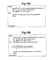
- An example of the interrupt process program in the case where the CPU 10 performs the low-speed operation is shown as the program 1 of Fig. 10A
- an example of the interrupt process program in the case of performing the high-speed operation is shown as the program 2 of Fig. 10B .
- the range from the label IRQ0/IRQ1 to the label W0 of each program example is a common process, and thus the command is executed in synchronization with the low-speed clock signal LCK.
- the process is executed in synchronization with the low-speed clock signal LCK even during the time until the oscillation of the high-speed clock signal HCK, of which the oscillation is already initiated before the CPU receives the interrupt notification, is stabilized.
- the system clock signal SCK is switched from the low-speed clock signal LCK to the high-speed clock signal HCK.
- the CAN communication process thereafter is performed in synchronization with the high-speed clock signal HCK.
- the system clock signal SCK is switched by the clk change command.
- This configuration has the following objects: one object is to prevent the entire data processor 1 from being unstable by entirely changing the system clock signal at an unexpected timing in case that the configuration is made such that the system clock signal is automatically entirely changed in response to stabilization of the oscillation of the high-speed clock signal; and the other object is to fix the time for executing the process after waiting for stabilization of the oscillation in case that the oscillation of the high-speed clock signal HCK is not yet stabilized at the time point of execution of the corresponding command.
- Fig. 9 shows an example of operation timing according to a comparative example in which the instruction to generate the oscillation of the high-speed clock is issued by the interrupt without using the trigger determination circuit 21 in case that the CPU 10 returns from the standby state and performs the high-speed operation.
- the CPU is activated by the interrupt, and the CPU initiates the interrupt sequence in synchronization with the low-speed clock signal.
- the interrupt sequence is completed, on the basis of the vector obtained in accordance therewith, the interrupt process is activated, and first the high-speed clock oscillation circuit is instructed to initiate the oscillation in case that the high-speed clock synchronization operation is necessary in accordance with the interrupt process program.
- the former T1 is set to be smaller than the latter T2. Consequently, in the operation that periodically repeats the high-speed clock synchronization operation based on the standby state and the standby cancellation, the average consumption current or the accumulated consumption current is reduced by employing the control of the standby cancellation at the timing shown in Fig. 8 .
- the low power consumption mode is not limited to the above description.
- the circuits, which are inactive in the low power consumption mode are not limited to the case where the supply of the power supply voltage is stopped, but the supply of the clock signal may be stopped. Further, instead of stopping of the supply of the power supply voltage, the supply of the clock signal may be stopped.
- the synchronization clock signal of the data processor is not limited to the two clock signals such as HCK and LCK.
- LCK and MCK are set as the second clock signals.
- LCK is set as the second clock signal
- MCK and HCK are set as the first clock signals.
- the first clock signal may be used as a frequency-divided multi-layer clock signal.
- the type of the circuit module provided in the data processor, the internal bus configuration of the data processor, and the like may be appropriately changed.
- the data processor is appropriate for a multi-CPU, and may have various kinds of accelerators, and the use applications thereof are not limited to this.
- the switching control of the clock switching circuit for switching the system clock signal from the low-speed clock signal to the high-speed clock signal is not limited to the case of using the interrupt.
- the switching control of the clock switching circuit for switching the system clock signal from the low-speed clock signal to the high-speed clock signal is not limited to the case of using the interrupt.
- by directly supplying the time-out signal of the oscillation stabilization latency timer to the switching circuit it may be used in the switching.
- the return trigger signal which is output by the CAN control module, is used as the external interrupt signal indicating the trigger to return from the standby mode.
- the network connected with the electronic control unit is not limited to the CAN, and may be the LIN (Local Interconnect Network) or the like, and the network is not restricted to the communication protocol of the on-vehicle LAN.
- LIN Local Interconnect Network
- the data processor and the electronic control unit of the present invention are not limited to the application for vehicle, and may be applied to various kinds of controls of home applications and industrial applications.
- the present invention can be broadly applied to available techniques in consideration of low power consumption in the case of clock oscillation of the data processor and the electronic control unit using the data processor.
- the invention can be applied to electronic control units of vehicles such as an automobile.
Landscapes
- Engineering & Computer Science (AREA)
- Theoretical Computer Science (AREA)
- Physics & Mathematics (AREA)
- General Engineering & Computer Science (AREA)
- General Physics & Mathematics (AREA)
- Power Sources (AREA)
- Microcomputers (AREA)
- Electronic Switches (AREA)
Applications Claiming Priority (1)
| Application Number | Priority Date | Filing Date | Title |
|---|---|---|---|
| PCT/JP2010/058549 WO2011145198A1 (fr) | 2010-05-20 | 2010-05-20 | Processeur de données et unité de commande électronique |
Publications (1)
| Publication Number | Publication Date |
|---|---|
| EP2573683A1 true EP2573683A1 (fr) | 2013-03-27 |
Family
ID=44991322
Family Applications (1)
| Application Number | Title | Priority Date | Filing Date |
|---|---|---|---|
| EP10851762A Withdrawn EP2573683A1 (fr) | 2010-05-20 | 2010-05-20 | Processeur de données et unité de commande électronique |
Country Status (5)
| Country | Link |
|---|---|
| US (1) | US20130067258A1 (fr) |
| EP (1) | EP2573683A1 (fr) |
| JP (1) | JPWO2011145198A1 (fr) |
| CN (1) | CN102906732A (fr) |
| WO (1) | WO2011145198A1 (fr) |
Cited By (3)
| Publication number | Priority date | Publication date | Assignee | Title |
|---|---|---|---|---|
| WO2016148792A1 (fr) * | 2015-03-13 | 2016-09-22 | Qualcomm Incorporated | Appareils, procédés et systèmes destinés à une commutation d'horloge exempte d'impulsions transitoires |
| US10324521B2 (en) | 2012-10-17 | 2019-06-18 | Semiconductor Energy Laboratory Co., Ltd. | Microcontroller and method for manufacturing the same |
| CN111510111A (zh) * | 2020-04-27 | 2020-08-07 | 上海华虹宏力半导体制造有限公司 | 振荡模块及芯片上电方法 |
Families Citing this family (18)
| Publication number | Priority date | Publication date | Assignee | Title |
|---|---|---|---|---|
| US9841804B2 (en) * | 2012-02-22 | 2017-12-12 | Silicon Laboratories Inc. | Clocking a processor |
| US10284073B2 (en) * | 2012-04-25 | 2019-05-07 | Hamilton Sundstrand Corporation | Power supply built-in testing |
| US9043457B2 (en) | 2012-10-25 | 2015-05-26 | Qualcomm Incorporated | Dynamic adjustment of an interrupt latency threshold and a resource supporting a processor in a portable computing device |
| JP6070321B2 (ja) * | 2013-03-21 | 2017-02-01 | 富士通株式会社 | 携帯情報端末、制御方法、制御プログラム |
| JP6229552B2 (ja) * | 2014-03-05 | 2017-11-15 | 株式会社デンソー | 制御装置、及び、初期化プログラム |
| US10447461B2 (en) * | 2015-12-01 | 2019-10-15 | Infineon Technologies Austria Ag | Accessing data via different clocks |
| JP6762656B2 (ja) * | 2016-03-23 | 2020-09-30 | 日本無線株式会社 | Cpuスタンバイ復帰構造 |
| US10191124B2 (en) * | 2016-08-26 | 2019-01-29 | Sii Semiconductor Corporation | Sensor circuit |
| CN107066250A (zh) * | 2017-01-05 | 2017-08-18 | 珠海格力电器股份有限公司 | 功耗控制电路、电器设备及功耗控制方法 |
| CN107239133A (zh) * | 2017-06-01 | 2017-10-10 | 合肥联宝信息技术有限公司 | 一种智能设备的控制方法及装置 |
| CN110045989B (zh) * | 2019-03-14 | 2023-11-14 | 合肥雷芯智能科技有限公司 | 一种动态切换式低功耗处理器 |
| WO2020237635A1 (fr) * | 2019-05-31 | 2020-12-03 | 华为技术有限公司 | Ensemble interface, puce et dispositif électronique |
| JP7359047B2 (ja) * | 2020-03-16 | 2023-10-11 | セイコーエプソン株式会社 | リアルタイムクロック装置 |
| JP7407046B2 (ja) * | 2020-03-26 | 2023-12-28 | 本田技研工業株式会社 | 音声出力の制御方法および音声出力制御装置 |
| JP2022096389A (ja) * | 2020-12-17 | 2022-06-29 | キオクシア株式会社 | 半導体集積回路、半導体記憶装置、および制御方法 |
| KR20220122186A (ko) * | 2021-02-26 | 2022-09-02 | 삼성전자주식회사 | 전력 관리 집적 회로 및 이를 포함하는 전자 장치 |
| JP2022134510A (ja) * | 2021-03-03 | 2022-09-15 | キヤノン株式会社 | 通信装置、通信装置の制御方法、プログラム、および記憶媒体 |
| CN113406992B (zh) * | 2021-05-25 | 2022-11-11 | 威胜集团有限公司 | 系统时钟的控制方法、处理装置和可读存储介质 |
Family Cites Families (14)
| Publication number | Priority date | Publication date | Assignee | Title |
|---|---|---|---|---|
| JPS61147324A (ja) * | 1984-12-20 | 1986-07-05 | Matsushita Electric Ind Co Ltd | クロツク制御回路 |
| US5261082A (en) * | 1987-11-20 | 1993-11-09 | Hitachi, Ltd. | Semiconductor integrated circuit having a plurality of oscillation circuits |
| JP2614877B2 (ja) * | 1987-11-20 | 1997-05-28 | 株式会社日立製作所 | 半導体集積回路装置 |
| JP3490222B2 (ja) * | 1996-07-19 | 2004-01-26 | カルソニックカンセイ株式会社 | マイクロコンピュータ装置 |
| JPH1049248A (ja) * | 1996-07-29 | 1998-02-20 | Sharp Corp | マイクロコンピュータ |
| JP2000112586A (ja) * | 1998-10-06 | 2000-04-21 | Canon Inc | データ通信装置、方法および記憶媒体 |
| JP2001344039A (ja) * | 2000-03-31 | 2001-12-14 | Seiko Epson Corp | 情報処理装置、情報処理装置の制御方法および情報処理装置の制御プログラム |
| JP2004070722A (ja) * | 2002-08-07 | 2004-03-04 | Renesas Technology Corp | マイクロコンピュータ |
| JP2004234463A (ja) * | 2003-01-31 | 2004-08-19 | Denso Corp | A/d変換データ入力システム |
| JP3958720B2 (ja) * | 2003-07-22 | 2007-08-15 | 沖電気工業株式会社 | クロック制御回路とクロック制御方法 |
| US7454645B2 (en) * | 2005-03-31 | 2008-11-18 | Cypress Semiconductor Corp. | Circuit and method for monitoring the status of a clock signal |
| JP4905354B2 (ja) * | 2005-09-20 | 2012-03-28 | 富士通株式会社 | 電源電圧調整装置 |
| JP4997035B2 (ja) * | 2006-11-22 | 2012-08-08 | 株式会社リコー | 画像処理装置およびリファレンスクロック供給方法 |
| JP2010102491A (ja) * | 2008-10-23 | 2010-05-06 | Denso Corp | マイクロコンピュータチップ |
-
2010
- 2010-05-20 EP EP10851762A patent/EP2573683A1/fr not_active Withdrawn
- 2010-05-20 JP JP2012515681A patent/JPWO2011145198A1/ja active Pending
- 2010-05-20 CN CN2010800668677A patent/CN102906732A/zh active Pending
- 2010-05-20 US US13/698,650 patent/US20130067258A1/en not_active Abandoned
- 2010-05-20 WO PCT/JP2010/058549 patent/WO2011145198A1/fr active Application Filing
Non-Patent Citations (1)
| Title |
|---|
| See references of WO2011145198A1 * |
Cited By (5)
| Publication number | Priority date | Publication date | Assignee | Title |
|---|---|---|---|---|
| US10324521B2 (en) | 2012-10-17 | 2019-06-18 | Semiconductor Energy Laboratory Co., Ltd. | Microcontroller and method for manufacturing the same |
| WO2016148792A1 (fr) * | 2015-03-13 | 2016-09-22 | Qualcomm Incorporated | Appareils, procédés et systèmes destinés à une commutation d'horloge exempte d'impulsions transitoires |
| US9509318B2 (en) | 2015-03-13 | 2016-11-29 | Qualcomm Incorporated | Apparatuses, methods, and systems for glitch-free clock switching |
| CN111510111A (zh) * | 2020-04-27 | 2020-08-07 | 上海华虹宏力半导体制造有限公司 | 振荡模块及芯片上电方法 |
| CN111510111B (zh) * | 2020-04-27 | 2024-03-15 | 上海华虹宏力半导体制造有限公司 | 振荡模块及芯片上电方法 |
Also Published As
| Publication number | Publication date |
|---|---|
| CN102906732A (zh) | 2013-01-30 |
| WO2011145198A1 (fr) | 2011-11-24 |
| JPWO2011145198A1 (ja) | 2013-07-22 |
| US20130067258A1 (en) | 2013-03-14 |
Similar Documents
| Publication | Publication Date | Title |
|---|---|---|
| EP2573683A1 (fr) | Processeur de données et unité de commande électronique | |
| JP3505018B2 (ja) | 半導体集積回路 | |
| US7032117B2 (en) | Dynamic power control in integrated circuits | |
| US20160320998A1 (en) | Control device, control method, computer program product, and electronic device | |
| JP4665846B2 (ja) | マイクロコンピュータ及び電子制御装置 | |
| US10571993B2 (en) | Micro controller unit | |
| JP2008107914A (ja) | マイクロコンピュータ、プログラム及び車両用電子制御装置 | |
| JP4715760B2 (ja) | マイクロコンピュータ及び制御システム | |
| JP2008102830A (ja) | マイクロコンピュータ、プログラム及び車両用電子制御装置 | |
| EP2247992B1 (fr) | Circuits et procédés de commutation de signaux d'horloge | |
| US8751842B2 (en) | Microcontroller and method of controlling the same | |
| US20150268715A1 (en) | Semiconductor device and automobile control system | |
| JP5324340B2 (ja) | マイクロコンピュータ | |
| JP2007058347A (ja) | 受信装置及びその制御方法 | |
| JP6198175B2 (ja) | 通信回路 | |
| JP2006065471A (ja) | 半導体集積回路およびその節電制御方法および節電制御プログラム | |
| JP2010097427A (ja) | 処理装置、処理方法及びコンピュータプログラム | |
| JP2005186770A (ja) | 車載装置及びその電源制御方法 | |
| JP4219601B2 (ja) | 情報処理装置 | |
| JP3711849B2 (ja) | マイクロコンピュータ | |
| JP2002049610A (ja) | マイクロコンピュータの動作クロック設定装置 | |
| JP2006072698A (ja) | 省電力対応装置 | |
| JP5682783B2 (ja) | 信号入力用回路 | |
| JP2004234463A (ja) | A/d変換データ入力システム | |
| US8677164B2 (en) | Microcomputer and control method thereof |
Legal Events
| Date | Code | Title | Description |
|---|---|---|---|
| PUAI | Public reference made under article 153(3) epc to a published international application that has entered the european phase |
Free format text: ORIGINAL CODE: 0009012 |
|
| 17P | Request for examination filed |
Effective date: 20121120 |
|
| AK | Designated contracting states |
Kind code of ref document: A1 Designated state(s): AL AT BE BG CH CY CZ DE DK EE ES FI FR GB GR HR HU IE IS IT LI LT LU LV MC MK MT NL NO PL PT RO SE SI SK SM TR |
|
| DAX | Request for extension of the european patent (deleted) | ||
| STAA | Information on the status of an ep patent application or granted ep patent |
Free format text: STATUS: THE APPLICATION HAS BEEN WITHDRAWN |
|
| 18W | Application withdrawn |
Effective date: 20131203 |