EP2546665B1 - Electronic device, and open circuit detecting system, detecting method thereof - Google Patents
Electronic device, and open circuit detecting system, detecting method thereof Download PDFInfo
- Publication number
- EP2546665B1 EP2546665B1 EP11007589.2A EP11007589A EP2546665B1 EP 2546665 B1 EP2546665 B1 EP 2546665B1 EP 11007589 A EP11007589 A EP 11007589A EP 2546665 B1 EP2546665 B1 EP 2546665B1
- Authority
- EP
- European Patent Office
- Prior art keywords
- capacitance
- parasitic capacitor
- open circuit
- circuit
- status
- Prior art date
- Legal status (The legal status is an assumption and is not a legal conclusion. Google has not performed a legal analysis and makes no representation as to the accuracy of the status listed.)
- Active
Links
- 238000000034 method Methods 0.000 title claims description 21
- 239000003990 capacitor Substances 0.000 claims description 145
- 230000003071 parasitic effect Effects 0.000 claims description 140
- 238000005070 sampling Methods 0.000 claims description 47
- 238000012360 testing method Methods 0.000 claims description 39
- 239000004020 conductor Substances 0.000 claims description 22
- 239000000306 component Substances 0.000 claims description 17
- 238000001514 detection method Methods 0.000 claims description 7
- 238000007599 discharging Methods 0.000 claims description 6
- 230000000630 rising effect Effects 0.000 claims description 3
- 230000006870 function Effects 0.000 description 9
- 238000010586 diagram Methods 0.000 description 8
- 230000000694 effects Effects 0.000 description 4
- 239000011521 glass Substances 0.000 description 4
- 230000001939 inductive effect Effects 0.000 description 2
- 230000015556 catabolic process Effects 0.000 description 1
- 238000006731 degradation reaction Methods 0.000 description 1
- 230000001419 dependent effect Effects 0.000 description 1
- 238000005516 engineering process Methods 0.000 description 1
- 230000003993 interaction Effects 0.000 description 1
- 230000002452 interceptive effect Effects 0.000 description 1
Images


Classifications
-
- G—PHYSICS
- G01—MEASURING; TESTING
- G01R—MEASURING ELECTRIC VARIABLES; MEASURING MAGNETIC VARIABLES
- G01R31/00—Arrangements for testing electric properties; Arrangements for locating electric faults; Arrangements for electrical testing characterised by what is being tested not provided for elsewhere
- G01R31/50—Testing of electric apparatus, lines, cables or components for short-circuits, continuity, leakage current or incorrect line connections
- G01R31/54—Testing for continuity
-
- G—PHYSICS
- G01—MEASURING; TESTING
- G01R—MEASURING ELECTRIC VARIABLES; MEASURING MAGNETIC VARIABLES
- G01R31/00—Arrangements for testing electric properties; Arrangements for locating electric faults; Arrangements for electrical testing characterised by what is being tested not provided for elsewhere
- G01R31/28—Testing of electronic circuits, e.g. by signal tracer
-
- G—PHYSICS
- G01—MEASURING; TESTING
- G01R—MEASURING ELECTRIC VARIABLES; MEASURING MAGNETIC VARIABLES
- G01R31/00—Arrangements for testing electric properties; Arrangements for locating electric faults; Arrangements for electrical testing characterised by what is being tested not provided for elsewhere
- G01R31/50—Testing of electric apparatus, lines, cables or components for short-circuits, continuity, leakage current or incorrect line connections
- G01R31/52—Testing for short-circuits, leakage current or ground faults
-
- G—PHYSICS
- G01—MEASURING; TESTING
- G01R—MEASURING ELECTRIC VARIABLES; MEASURING MAGNETIC VARIABLES
- G01R31/00—Arrangements for testing electric properties; Arrangements for locating electric faults; Arrangements for electrical testing characterised by what is being tested not provided for elsewhere
- G01R31/50—Testing of electric apparatus, lines, cables or components for short-circuits, continuity, leakage current or incorrect line connections
- G01R31/66—Testing of connections, e.g. of plugs or non-disconnectable joints
-
- G—PHYSICS
- G01—MEASURING; TESTING
- G01R—MEASURING ELECTRIC VARIABLES; MEASURING MAGNETIC VARIABLES
- G01R31/00—Arrangements for testing electric properties; Arrangements for locating electric faults; Arrangements for electrical testing characterised by what is being tested not provided for elsewhere
- G01R31/50—Testing of electric apparatus, lines, cables or components for short-circuits, continuity, leakage current or incorrect line connections
- G01R31/64—Testing of capacitors
Definitions
- the present disclosure relates generally to circuit detection technology, and more particularly, to an electronic device, a system and a method for determining an open circuit status of an object circuit.
- AC alternating current
- DC direct current
- FIG. 1 An alternating current detecting system for detecting an open circuit is illustrated in FIG. 1 .
- An object circuit under test is equivalent to an equivalent resistor and an equivalent capacitor connected to the resistor in series.
- an AC source is connected between one end of the object circuit and the ground.
- the other end of the object circuit is connected to one end of a detecting module.
- This detection system has a physical ground loop.
- An AC signal generated by the AC source is transmitted to the detecting module through the object circuit.
- the detecting module can determine the status of the object circuit based on the AC signal's frequency or magnitude.
- FIG. 2 A direct current detecting system for detecting an open circuit is illustrated in FIG. 2 .
- An object circuit under test can be represented as an equivalent resistor.
- a DC signal generated by a DC source is applied to one end of the object circuit.
- the other end of the object circuit is connected to one end of a detecting module.
- the other end of the DC source and the other end of the detecting module are also connected to the ground.
- This detection system has a physical ground loop.
- the detecting module can determine whether the object circuit is open through acquiring the current of the DC signal or the voltage of the DC signal.
- a typical detecting system has a physical ground loop.
- Various wires within the system may affect the detecting system.
- a detection system may not always determine the true status of the object circuit.
- the equivalent resistance generated by wires in an alternating current detecting system may be large.
- V ( noise ) I ( noise )* Z ( line )
- I(noise) I ( noise )* Z ( line )
- a weak noise (I(noise)) will become a large interfering signal (V(noise)) while it flows through the resistor (Z(line)).
- One solution to this problem is adding a filter module. However, only specific frequencies can be filtered by the filter module. While filters are useful for eliminating unwanted frequencies from a given signal, some desired frequencies in the signal may also be removed from the signal thus causing a loss of desired features.
- the frequency of the AC signal must be increased. This increase in frequency will result in a potential degradation of an AC signal due to the parasitic capacitance and loop impedance. An extra compensating circuit may be needed to eliminate these undesired effects.
- the long thin grounding wires in a DC system reduce the voltage as well as increase the system noise.
- the voltage amplitude and the level of sampling resolution must be increased in these systems.
- Patent documents US 6130530 A , US 6098027 A and US 2008157782 A1 disclose open circuit detection systems.
- the open circuit detection systems are connected to two ends of a circuit.
- these systems are not suitable for testing circuits that do not have two openings.
- An open circuit detecting system is configured to connect to an object circuit for obtaining an electrical signal through a virtual ground induced by characteristic impedance of a parasitic capacitor and for determining whether the object circuit is in an open circuit state according to the electrical signal.
- the electrical signal obtained by the open circuit detecting system indicates that the capacitance of the parasitic capacitor in normal circuit is greater than the capacitance of the parasitic capacitor in an open circuit status.
- the open circuit detecting system thus includes a test unit, a stray-capacitance boosting unit, a sampling unit, and a signal processing unit; wherein the sampling unit is a sampling resistor, the signal processing unit comprises an inverter, a comparator connected to the inverter, and an "AND" gate connected to the comparator, one end of the test unit is connected to a power supply, and the other end of the test unit is connected to a first input of the stray-capacitance boosting unit, a second input of the stray-capacitance boosting unit is connected to the object circuit, an output of the stray-capacitance boosting unit is connected to one end of the sampling resistor, and the other end of the sampling resistor is connected to the ground, an input of the inverter is connected to the common point of the stray-capacitance boosting unit and the sampling resistor, an output of the inverter is connected to a negative terminal of the comparator, a positive terminal of the comparator
- test unit is configured to generate a burst pulse for charging the parasitic capacitor
- sampling unit is configured to discharge the charged parasitic capacitor
- the rising edge of the burst pulse is before the falling edge of the burst pulse.
- the stray-capacitance boosting unit is an Insulated Gate Bipolar Transistor, a triode, or a Darlington Transistor.
- the signal processing unit is configured to convert the electrical signal into several numbers of pulses corresponding to the capacitance of the parasitic capacitor.
- a method for detecting open circuit includes the steps of: acquiring an electrical signal through a virtual ground induced by characteristic impedance of a parasitic capacitor; and determining whether the object circuit is open according to the electrical signal.
- the electrical signal indicates the capacitance of the parasitic capacitor in normal circuit is greater than the capacitance of the parasitic capacitor in open circuit.
- a method for detecting open circuit according to the present invention using the open circuit detecting system as outlined above, wherein a parasitic capacitor exists between the object circuit and ground, said parasitic capacitor having a characteristic impedance, which represents all the parasitic capacitance that exists between conductors, conductors or components and ground, or the capacitance that exists between components comprises the steps of: acquiring an electrical signal corresponding to the parasitic capacitor that exists between the object circuit and ground, said parasitic capacitor having a characteristic impedance, which represents all the parasitic capacitance that exists between conductors, conductors or components and ground, or the capacitance that exists between components; and determining whether the object circuit is in an open circuit status or in a normal circuit status according to the electrical signal by determining the capacitance of the parasitic capacitor; wherein the capacitance of the parasitic capacitor in a normal circuit status is greater than the capacitance of the parasitic capacitor in an open circuit status.
- the step of testing includes: generating a burst pulse for charging the parasitic capacitor, and discharging the parasitic capacitor though a sampling unit to generate the electrical signal.
- the method further includes the steps of: converting the electrical signal into an identification signal; and determining whether the object circuit is open according to the identification signal.
- An electronic device includes an object circuit and an open circuit detecting system as outlined above.
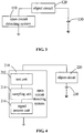
- FIG. 3 a first embodiment of an open circuit detecting system 110 is illustrated serving for a better understanding of the present invention.
- the open circuit detecting system 110 is a circuit or device with the function of detecting an open circuit status of the object circuit 120.
- the object circuit 120 is a circuit or device under test in which an open circuit may exist. In a normal circuit status, one end of the object circuit 120 is connected to the open circuit detecting system 110.
- a parasitic capacitor 130 having a characteristic impedance exists between the object circuit 120 and ground.
- the parasitic capacitor 130 is the capacitance that exists between conductors of the circuit, conductors or components and ground, or the capacitance that exists between components. For the convenience of description, the parasitic capacitor 130 is intended to represent all the parasitic capacitance of the object circuit 120.
- the capacitance is proportional to the length of conductors in a circuit.
- the parasitic capacitor 130 in a normal circuit is greater than the parasitic capacitor 130 in open circuit, since the conductor in a normal circuit is longer than the conductor in an open circuit.
- the open circuit detecting system 110 is arranged for inducing an electrical signal and the electrical signal is used for determining whether the capacitance of the parasitic capacitor 130 is in a normal circuit status, i.e. is greater than the capacitance of the parasitic capacitor 130 in open circuit.
- the parasitic capacitor 130 is connected to a virtual ground by a characteristic impedance. In other words, the parasitic capacitor 130 is not connected to ground in reality, but the potential difference between the parasitic capacitor 130 and ground is zero.
- the open circuit detecting system 110 begins to work under the reference potential and provides the electrical signal which indicates that the circuit status of the object circuit 120 is an open circuit status.
- a parasitic capacitor 230 exists, which is the capacitance that exists between conductors of the circuit, between conductors and ground, between components and ground, or between components.
- the parasitic capacitor 230 is intended to represent all the parasitic capacitor of an object circuit 220.
- the capacitance is proportional to the length of conductors in a circuit.
- the parasitic capacitor 230 in a normal circuit status is greater than the parasitic capacitor 230 in an open circuit, since the conductor in a normal circuit is longer than the conductor in open circuit.
- the open circuit detecting system 210 is arranged for inducing an electrical signal and the electrical signal is used for determining whether the capacitance of the parasitic capacitor 230 in a normal circuit status, i.e. is greater than the capacitance of the parasitic capacitor 230 in open circuit.
- one end of the open circuit detecting system 210 is connected to the ground, and the other end of the open circuit detecting system 210 is connected to the object circuit 220.
- the open circuit detecting system 210 is a circuit or device with the function of detecting an open circuit status.
- the open circuit detecting system 210 includes a test unit 212 connected to the object circuit 220, a sampling unit 214 connected to the test unit 212, and a signal processing unit 216 connected to the sampling unit 214.
- the test unit 212 is used for testing the capacitance of the parasitic capacitor 230.
- the test unit 212 tests the capacitance of the parasitic capacitor 230 by charging the parasitic capacitor 230 or a resonance circuit including the parasitic capacitor 230. If the test unit 212 provides the same testing signals, charging time constants or discharging time constants in an open circuit status and a normal circuit status are different because of different magnitude of the parasitic capacitor.
- the sampling unit 214 reflects the state of the parasitic capacitor 230.
- the sampling unit 214 may be a sampling resistor or another circuit with sampling function.
- the electrical signal which can be easily observed is sampled by the sampling unit 214.
- the charging time constant in an open circuit status is smaller than the charging time constant in a normal circuit status.
- the parasitic capacitor 230 discharges though the sampling unit 214 after being charged by the test unit 212.
- the electrical signal which can be easily observed is sampled by the sampling unit 214.
- the parasitic capacitor 230 in a normal circuit status is greater than the parasitic capacitor 230 in an open circuit status.
- the status of the circuit can be determined by an experienced person or a machine.
- resonance frequencies vary in different resonance circuits including different parasitic capacitors, identical resistors and identical inductors.
- the sampling unit 214 obtains a resonance signal from the resonance circuit including the test unit 212 and the parasitic capacitor 230.
- the status of the circuit can be determined by an experienced person or a machine.
- the signal processing unit 216 is added to convert the electrical signal into an identification signal which can be easily recognized by machines. "AND”, “OR”, “NOT” and comparison operations or combinations with other signals are performed by the signal processing unit 216 to convert the electrical signal obtained from the sampling unit 214 into the identification signal which can be easily recognized by machines.
- the identification signal is sent to a computer, a digital signal processor (DSP), an advanced RISC machine and so on for computing or displaying a result based on the identification signal obtained.
- DSP digital signal processor
- the parasitic capacitor 230 is connected to a virtual ground by a characteristic impedance. In other words, the parasitic capacitor 230 is not connected to ground in reality, but a potential difference between the parasitic capacitor 230 and ground is zero.
- the open circuit detecting system 210 begins to work after receiving a reference potential.
- the open circuit detecting system 210 checks the object circuit 220 to find out whether the status of the object circuit 220 is an open circuit status.
- the test unit 212 begins to test the capacitance of the parasitic capacitor 230 by charging the parasitic capacitor 230 or the resonant circuit including the parasitic capacitor 230. As to the object circuit 220, the parasitic capacitor 230 in a normal circuit status is greater than the parasitic capacitor 230 in an open circuit status.
- the sampling unit 214 provides the electrical signal when the parasitic capacitor 230 discharges through the sampling unit 214.
- the electrical signal can be easily observed or processed by a machine.
- the signal processing unit 216 converts the electrical signal into the identification signal which can be easily recognized by machines. "AND”, “OR”, “NOT” functions, comparison operations or combinations with other signals are performed by the signal processing unit 216 to convert the electrical signal obtained from the sampling unit 214 into the identification signal which can be easily recognized by machines.
- the identification signal may be sent to a computer for computing or displaying, thus the status of the object circuit 220 can be provided by a computer.
- FIG. 5 and FIG 6 a third embodiment of an open circuit detecting system 310 according to the present invention is illustrated.
- One end of the open circuit detecting system 310 is connected to ground.
- a parasitic capacitor 330 exists between the object circuit 320 and ground.
- the parasitic capacitor 330 is the capacitance that exists between conductors of the circuit, between conductors and ground, between components and ground, or between components and has no physical reality.
- the parasitic capacitor 330 is intended to represent all the parasitic capacitance in the object circuit 320.
- the detecting relates only to the parasitic capacitor 330, for the convenience of description, the object circuit 320 is omitted in FIG. 6 .
- the parasitic capacitor 330 has its own resistance, and therefore, an equivalent capacitor and an equivalent resistor are connected in series in FIG. 6 for representing the parasitic capacitor 330.
- the open circuit detecting system 310 is a circuit or device with the function of detecting an open circuit status.
- the open circuit detecting system 310 includes a test unit 312, a stray-cap booster unit 313 connected to the test unit 312 and the parasitic capacitor 330, a sampling unit 314 connected to the stray-cap booster unit 313, and a signal processing unit 316 connected to the sampling unit 314.
- the test unit 312 serves for generating a burst pulse. One end of the test unit 312 is connected to a power supply, and the other end of the test unit 312 is connected to a first input of the stray-capacitance boosting unit 313.
- the test unit 312 is electrically connected to the parasitic capacitor 330 though the stray-capacitance boosting unit 313. Therefore, the test unit 312 charges the parasitic capacitor 330 though the stray-capacitance boosting unit 313.
- the stray-capacitance boosting unit 313 is configured for amplifying charging and discharging effects. It may be an Insulated Gate Bipolar Transistor, a transistor, a Darlington Transistor or other circuit with an amplifying function.
- the first input of the stray-capacitance boosting unit 313 is connected to the test unit 312, a second input of the stray-capacitance boosting unit 313 is connected to the parasitic capacitor 330, and an output of the stray-capacitance boosting unit 313 is connected to the common point of the sampling unit 314 and the signal processing unit 316.
- the stray-capacitance boosting unit 313 is a transistor, the first input of the stray-capacitance boosting unit 313 is an emitter of the transistor, the second input of the stray-capacitance boosting unit 313 is a base of the transistor, and the output of the stray-capacitance boosting unit 313 is a collector of the transistor.
- a burst pulse generated by the test unit 312 charges the parasitic capacitor 330 via the emitter of the transistor and the base of the transistor.
- the emitter-base junction is forward biased until the voltage of the parasitic capacitor 330 rises up to a preset voltage.
- Working in the linear region of the transistor the transistor is in active mode, thus charging and discharging effects are amplified.
- a discharge current flows through the sampling unit 314 and then forms a voltage signal.
- the sampling unit 314 reflects the state of the parasitic capacitor 330.
- the sampling unit 314 can be a sampling resistor or other circuits with sampling function. One end of the sampling unit 314 is connected to the common point of the stray-capacitance boosting unit 313 and the signal processing unit 316, and the other end of the sampling unit 314 is connected to ground.
- the discharge current of the parasitic capacitor 330 flows from the stray-capacitance boosting unit 313 to ground via the sampling unit 314, and the voltage signal is sampled from the common point of the stray-capacitance boosting unit 313 and the sampling unit 314. At last, the voltage signal is sent to the signal processing unit 316.
- the signal processing unit 316 includes an inverter 3162, a comparator 3164 connected to the inverter 3162 and an "AND" gate 3166 connected to the comparator 3164.
- An input of the inverter 3162 is connected to the common point of the stray-capacitance boosting unit 313 and the sampling unit 314, and an output of the inverter 3162 is connected to a negative terminal of the comparator 3164.
- the inverter 3162 inverts the voltage signal provided by the sampling unit 314.
- the inverter 3162 has a relatively high input impedance so that it has an insignificant effect on the voltage signal.
- a reference voltage is applied to a positive terminal of the comparator 3164, the negative terminal of the comparator 3164 is connected to the output of the inverter 3162.
- the output voltage of the comparator 3164 is high-level. Otherwise, the output voltage of the comparator 3164 is low-level.
- a first input of the "AND” gate 3166 is connected to the comparator 3164, a second input of the “AND” gate 3166 is used to receive gate pulses. Only the first input of the "AND” gate 3166 and the second input of the “AND” gate 3166 are both high-level, an output of the "AND” gate 3166 is high-level. That is, when the first input of the "AND” gate 3166 is high-level, the output of the "AND” gate 3166 outputs gate pulses. Otherwise, when the first input of the "AND” gate 3166 is low-level, the "AND” gate 3166 will not output any signal.
- the parasitic capacitor 330 is connected to a virtual ground by a characteristic impedance. In other words, the parasitic capacitor 330 is not connected to ground in reality, but the potential difference between the parasitic capacitor 130 and the ground is zero.
- the open circuit detecting system 310 begins to work under the reference potential. The open circuit detecting system 310 begins to determine whether the circuit status is an open circuit status.
- the test unit 312 generates a burst pulse 4 10.
- the burst pulse 410 is a square wave signal having a rising edge before the failing edge.
- the inverter 3162, the comparator 3164 and the "AND" gate are enabled.
- the burst pulse 410 charges the parasitic capacitor 330. Because the equivalent resistor is low, the charging process is finished in a short time.
- the discharge current is amplified by the stray-capacitance boosting unit 313 and flows to the sampling unit 314. Then, the discharge current forms the voltage signal at the sampling unit 314.
- the voltage signal is changed into an inverter output signal 420 by the inverter 3162.
- the inverter output signal 420 is sent to the negative terminal of the comparator 3164 and compared with a reference voltage 402 sent to the positive terminal of the comparator 3164.
- a reference voltage 402 sent to the positive terminal of the comparator 3164.
- the parasitic capacitor 330 in a normal circuit status is greater than the parasitic capacitor 330 in an open circuit status; for the convenience of description, the parasitic capacitor 330 in a normal circuit status is called a "big capacitor”. On the contrary, the parasitic capacitor 330 in an open circuit status is called a "small capacitor”. Because of the discharging characteristics of the capacitor, the inverter output signal 420 rises up slowly.
- a signal line 422 of the big capacitor in the inverter output signal 420 rises up more slowly than a signal line 424 of the small capacitor in the inverter output signal 420.
- the duty ratio of a big capacitor comparator output signal 430 is greater than a small capacitor comparator output signal 440.
- the number of pulses of a big capacitor "AND" gate output signal 460 is larger than that of a small capacitor “AND” gate output signal 470.
- the number of pulses is sent to the processor, such as a computer, digital signal processor (DSP), a advanced RISC machines or the like, for computing or displaying.
- DSP digital signal processor
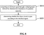
- FIG. 8 a first embodiment of a method for detecting an open circuit status according to the present invention is illustrated.
- Step S810 represents acquiring an electrical signal corresponding to a characteristic impedance of the parasitic capacitor.
- the parasitic capacitor is not connected to the ground in reality, but the potential difference between the parasitic capacitor and ground is zero.
- the open circuit detecting system begins to work under the reference potential and provides the electrical signal which indicates that the circuit status of the object circuit is an open status. Because the parasitic capacitor cannot be directly observed, the parasitic capacitor is charged for generating the electrical signal which can be easily observed.
- Step S820 represents determining whether the object circuit is an open circuit status, according to the electrical signal.
- the status of the circuit could be determined by an experienced person or a machine. More specifically, the electrical signal indicates the capacitance of the parasitic capacitor in a normal circuit status is greater than the capacitance of the parasitic capacitor in an open circuit status.
- FIG.9 a third embodiment of a method for detecting an open circuit status according to the present invention is illustrated.
- Step S910 represents connecting a parasitic capacitor to a virtual ground, in correspondence to the characteristic impedance of the parasitic capacitor.
- the parasitic capacitor is connected to a virtual ground by characteristic impedance. In other words, the parasitic capacitor is not connected to ground in reality, but the potential difference between the parasitic capacitor and ground is zero.
- Step S920 represents testing the capacitance of the parasitic capacitor and generating an electrical signal representing the capacitance of the parasitic capacitor. Because the parasitic capacitor cannot be directly observed, the parasitic capacitor is charged for generating the electrical signal which can be easily observed.
- Step S930 represents converting the electrical signal into an identification signal.
- a signal processing unit is added to convert the electrical signal into an identification signal.
- "AND”, “OR”, “NOT” functions and comparison operations or combinations with other signals can be used in the converting process.
- step S940 it is determined whether the status of the object circuit is an open circuit status, according to the identification signal.
- the identification signal is sent to the computer for computing or displaying after the identification signal was obtained.
- the status of the object circuit is determined.
- the capacitance of the parasitic capacitor in a normal circuit status is greater than the capacitance of the parasitic capacitor in an open circuit status.
- the open circuit detecting system and method as set forth above can be used in electronic devices, such as mobile phones, laptop computers, personal digital assistants, etc. If the open circuit detecting system is incorporated in an electronic device, the object circuit can be any other part of the electronic device.
- the open circuit detecting system is connected to the object circuit for acquiring an electrical signal through a virtual ground induced by a characteristic impedance of a parasitic capacitor and determining whether the object circuit is in an open circuit status or not electrically connected to the open circuit detecting system according to the electrical signal.
- the electrical signal obtained by the open circuit detecting system indicates that the capacitance of the parasitic capacitor in a normal circuit status is greater than that if the object circuit is in an open status internally or not electrically connected to the open circuit detecting system.
- the open circuit detecting system may be integrated in a chip and the object circuit may be a flex-cable or conductive trace on glass. If the flex-cable or conductive trace on glass is open internally or not electrically connected to the chip, the parasitic capacitor will be smaller than that in a normal state.
- Step S920 represents testing the capacitance of the parasitic capacitor and generating an electrical signal representing the capacitance of the parasitic capacitor. For the parasitic capacitor cannot be directly observed, the parasitic capacitor is charged for generating the electrical signal which is easy to be observed.
- Step S930 represents converting the electrical signal into an identification signal.
- a signal processing unit is added to convert the electrical signal into the identification signal.
- "AND”, “OR”, “NOT” and comparison operations or combining with the other signal can be used in the converting process.
- step S940 it is determined that whether the object circuit is open according to the identification signal.
- the identification signal is sent to the computer for computing or displaying after the identification signal was obtained.
- the state of the object circuit is found out.
- the capacitance of the parasitic capacitor in normal circuit is greater than the capacitance of the parasitic capacitor in open circuit.
- the open circuit detecting system and method can be used in electronic devices, such as mobile phones, laptop computers, personal digital assistants, etc. If the open circuit detecting system is incorporated in an electronic device, the object circuit can be any other parts of the electronic device.
- the open circuit detecting system is connected to the object circuit for getting an electrical signal through a virtual ground induced by characteristic impedance of a parasitic capacitor and determining whether the object circuit is open or not electrically connected to the open circuit detecting system according to the electrical signal.
- the electrical signal obtained by the open circuit detecting system indicates that the capacitance of the parasitic capacitor in normal circuit is greater than that if the object circuit is open internally or not electrically connected to the open circuit detecting system.
- the open circuit detecting system may be integrated in a chip and the object circuit may be a flex-cable or conductive trace on glass. If the flex-cable or conductive trace on glass is open internally or not electrically connected to the chip, the parasitic capacitor will be smaller than that in normal state.
Landscapes
- Physics & Mathematics (AREA)
- General Physics & Mathematics (AREA)
- Engineering & Computer Science (AREA)
- General Engineering & Computer Science (AREA)
- Measurement Of Resistance Or Impedance (AREA)
- Testing Of Short-Circuits, Discontinuities, Leakage, Or Incorrect Line Connections (AREA)
- Monitoring And Testing Of Exchanges (AREA)
- Testing Relating To Insulation (AREA)
Applications Claiming Priority (1)
| Application Number | Priority Date | Filing Date | Title |
|---|---|---|---|
| CN201110136822.9A CN102798787B (zh) | 2011-05-24 | 2011-05-24 | 电子设备及其断路检测系统与断路检测方法 |
Publications (3)
| Publication Number | Publication Date |
|---|---|
| EP2546665A2 EP2546665A2 (en) | 2013-01-16 |
| EP2546665A3 EP2546665A3 (en) | 2013-12-11 |
| EP2546665B1 true EP2546665B1 (en) | 2018-02-21 |
Family
ID=44799477
Family Applications (1)
| Application Number | Title | Priority Date | Filing Date |
|---|---|---|---|
| EP11007589.2A Active EP2546665B1 (en) | 2011-05-24 | 2011-09-16 | Electronic device, and open circuit detecting system, detecting method thereof |
Country Status (6)
| Country | Link |
|---|---|
| US (1) | US8947100B2 (ja) |
| EP (1) | EP2546665B1 (ja) |
| JP (1) | JP5547768B2 (ja) |
| KR (1) | KR101274821B1 (ja) |
| CN (1) | CN102798787B (ja) |
| TW (2) | TWM419924U (ja) |
Families Citing this family (17)
| Publication number | Priority date | Publication date | Assignee | Title |
|---|---|---|---|---|
| US9791494B2 (en) | 2012-01-20 | 2017-10-17 | Lear Corporation | Apparatus and method for diagnostics of a capacitive sensor |
| CN104854463B (zh) * | 2012-12-18 | 2019-12-20 | 飞利浦灯具控股公司 | 电缆系统中的问题检测 |
| US20150331034A1 (en) * | 2012-12-18 | 2015-11-19 | Koninklijke Philips N.V. | Problem detection in cable system |
| CN103941109B (zh) * | 2013-01-21 | 2017-07-28 | 宸鸿科技(厦门)有限公司 | 触控面板的测试装置 |
| JP6036429B2 (ja) * | 2013-03-18 | 2016-11-30 | 富士通株式会社 | 設計支援装置、設計支援プログラム、および設計支援方法 |
| JP5741967B2 (ja) * | 2013-04-23 | 2015-07-01 | 株式会社デンソー | 燃料性状センサ及びその故障検出方法 |
| US10260983B2 (en) | 2014-01-20 | 2019-04-16 | Lear Corporation | Apparatus and method for diagnostics of a capacitive sensor with plausibility check |
| US9678115B2 (en) * | 2014-05-13 | 2017-06-13 | General Electric Company | Contactless voltage sensing devices |
| US9759798B2 (en) * | 2014-05-13 | 2017-09-12 | General Electric Company | Calibration methods for voltage sensing devices |
| US9568533B2 (en) * | 2014-05-27 | 2017-02-14 | GM Global Technology Operations LLC | Method and apparatus for open-wire fault detection and diagnosis in a controller area network |
| CN105277834A (zh) * | 2014-06-18 | 2016-01-27 | 艾默生网络能源有限公司 | 一种检测电路 |
| KR101861705B1 (ko) * | 2016-12-29 | 2018-05-29 | 중앙대학교 산학협력단 | 표유 전계 에너지 하베스팅을 이용한 비접촉식 전압 측정 장치 |
| CN109541386A (zh) * | 2018-11-29 | 2019-03-29 | 厦门阳光恩耐照明有限公司 | 一种交直流驱动检测装置 |
| CN112213573B (zh) * | 2019-12-30 | 2023-06-23 | 蜂巢能源科技有限公司 | 高压互锁回路检测方法及电路 |
| CN111722149A (zh) * | 2020-06-12 | 2020-09-29 | 浪潮电子信息产业股份有限公司 | 一种线缆检测设备、方法、系统及计算机可读存储介质 |
| KR20230009580A (ko) * | 2021-07-09 | 2023-01-17 | 삼성전자주식회사 | 시그널 라인의 크랙을 검출하기 위한 전자 장치 및 전자 장치의 동작 방법 |
| CN114325501B (zh) * | 2021-12-31 | 2024-04-02 | 科博达技术股份有限公司 | Pdlc玻璃开路检测方法及其电路 |
Family Cites Families (19)
| Publication number | Priority date | Publication date | Assignee | Title |
|---|---|---|---|---|
| US5557209A (en) * | 1990-12-20 | 1996-09-17 | Hewlett-Packard Company | Identification of pin-open faults by capacitive coupling through the integrated circuit package |
| US6130530A (en) * | 1997-12-22 | 2000-10-10 | Hd Electric Company | Tester for power transformers and capacitors |
| JP4080550B2 (ja) * | 1998-02-05 | 2008-04-23 | コーニンクレッカ フィリップス エレクトロニクス エヌ ヴィ | 接続テスト方法 |
| US6098027A (en) * | 1998-07-02 | 2000-08-01 | Industrial Technology Research Institute | Charge mode open/short test circuit |
| JP3609687B2 (ja) * | 2000-04-11 | 2005-01-12 | 富士通株式会社 | 断線位置検出機能を備えた電子機器及び断線位置検出方法 |
| JP3701924B2 (ja) | 2002-03-29 | 2005-10-05 | インターナショナル・ビジネス・マシーンズ・コーポレーション | Elアレイ基板の検査方法及びその検査装置 |
| JP3527726B2 (ja) * | 2002-05-21 | 2004-05-17 | ウインテスト株式会社 | アクティブマトリクス基板の検査方法及び検査装置 |
| US6956336B2 (en) * | 2002-07-22 | 2005-10-18 | International Rectifier Corporation | Single chip ballast control with power factor correction |
| JP2005149768A (ja) | 2003-11-11 | 2005-06-09 | Shimadzu Corp | Tftアレイ検査方法及びtftアレイ検査装置 |
| KR100696856B1 (ko) * | 2004-09-30 | 2007-03-20 | 주식회사 디이엔티 | 평판표시장치의 tcp 출력핀 접속 오류 테스트 장치 및방법과 평판표시장치의 오류 테스트 시스템 |
| KR100932252B1 (ko) * | 2005-07-26 | 2009-12-16 | 가부시키가이샤 어드밴티스트 | 광수신 장치, 시험 장치, 광수신 방법, 시험 방법, 테스트모듈, 및 반도체 칩 |
| KR100796171B1 (ko) * | 2006-07-20 | 2008-01-21 | 마이크로 인스펙션 주식회사 | 접촉식 싱글사이드 프로브와 이를 이용한 도선의 단선 및단락 검사장치 및 그 방법 |
| US7986313B2 (en) * | 2007-01-03 | 2011-07-26 | Apple Inc. | Analog boundary scanning based on stray capacitance |
| US7698610B2 (en) * | 2007-07-25 | 2010-04-13 | Freescale Semiconductor, Inc. | Techniques for detecting open integrated circuit pins |
| US8024138B2 (en) * | 2008-02-01 | 2011-09-20 | International Rectifier Corporation | Power supply circuitry, collection and reporting of power supply parameter information |
| CN101369550B (zh) | 2008-08-12 | 2012-07-11 | 中国电子科技集团公司第四十五研究所 | 全自动引线键合机金线断线检测装置 |
| CN103985300B (zh) | 2009-11-16 | 2016-04-27 | 江苏省电力公司常州供电公司 | 电缆故障模拟及定位系统 |
| DE102011004288A1 (de) * | 2011-02-17 | 2012-08-23 | Robert Bosch Gmbh | Anordnung und Verfahren zur Verbindungsabrisserkennung an einem Schaltungsteil mit kapazitivem Verhalten |
| CN202083763U (zh) * | 2011-05-24 | 2011-12-21 | 宸鸿光电科技股份有限公司 | 电子设备及其断路检测系统 |
-
2011
- 2011-05-24 CN CN201110136822.9A patent/CN102798787B/zh active Active
- 2011-08-19 TW TW100215486U patent/TWM419924U/zh not_active IP Right Cessation
- 2011-08-19 TW TW100129702A patent/TWI465743B/zh active
- 2011-09-16 EP EP11007589.2A patent/EP2546665B1/en active Active
- 2011-10-28 KR KR1020110111377A patent/KR101274821B1/ko active IP Right Grant
- 2011-11-23 US US13/303,161 patent/US8947100B2/en active Active
-
2012
- 2012-03-29 JP JP2012076305A patent/JP5547768B2/ja active Active
Non-Patent Citations (1)
| Title |
|---|
| None * |
Also Published As
| Publication number | Publication date |
|---|---|
| EP2546665A2 (en) | 2013-01-16 |
| CN102798787A (zh) | 2012-11-28 |
| JP5547768B2 (ja) | 2014-07-16 |
| US20120299602A1 (en) | 2012-11-29 |
| JP2012242378A (ja) | 2012-12-10 |
| KR101274821B1 (ko) | 2013-06-13 |
| US8947100B2 (en) | 2015-02-03 |
| TW201248172A (en) | 2012-12-01 |
| CN102798787B (zh) | 2014-12-10 |
| EP2546665A3 (en) | 2013-12-11 |
| TWM419924U (en) | 2012-01-01 |
| KR20120131082A (ko) | 2012-12-04 |
| TWI465743B (zh) | 2014-12-21 |
Similar Documents
| Publication | Publication Date | Title |
|---|---|---|
| EP2546665B1 (en) | Electronic device, and open circuit detecting system, detecting method thereof | |
| US9524056B2 (en) | Capacitive voltage information sensing circuit and related anti-noise touch circuit | |
| CN106461720B (zh) | 包括电容耦合电场传感器的局部放电获取系统 | |
| KR20170110103A (ko) | 로고스키 코일 센서를 위한 전자 적분기 | |
| CN102968224A (zh) | 触控面板的控制电路及控制方法 | |
| CN101989221B (zh) | 印刷电路板测试参数设定文档生成系统及方法 | |
| CN202083763U (zh) | 电子设备及其断路检测系统 | |
| CN108983065B (zh) | 一种电压放大电路、检测电路及其电路检测方法 | |
| US10955462B2 (en) | Apparatus and method for frequency characterization of an electronic system | |
| CN210322887U (zh) | 一种自动采集数据的装置 | |
| CN115166400A (zh) | 一种检测装置、方法及系统 | |
| JP2016080526A (ja) | 絶縁性能診断装置および擬似キャパシタの容量値の設定方法 | |
| Park et al. | System-level ESD noise induced by secondary discharges at voltage suppressor devices in a mobile product | |
| JP3666408B2 (ja) | 半導体試験装置 | |
| CN104502723A (zh) | 高频治疗设备电阻检测电路 | |
| CN111398689A (zh) | 电容检测电路、电容检测系统和电子设备 | |
| Middelstaedt et al. | Methodology for optimizing radiated EMI Characteristics of power electronic circuits | |
| CN101427452A (zh) | 用于确定开关点的电力逆变器控制设备 | |
| CN219498934U (zh) | 一种剩余电流动作保护器及电子设备 | |
| JP3391310B2 (ja) | 容量性電子部品の絶縁抵抗測定装置 | |
| JP7215303B2 (ja) | 測定装置 | |
| CN214046000U (zh) | 测试电路及测试设备 | |
| US9217769B2 (en) | Ring oscillator testing with power sensing resistor | |
| CN213398730U (zh) | 电容检测电路、电容检测系统和电子设备 | |
| CN212905180U (zh) | 一种电子笔测试校准装置 |
Legal Events
| Date | Code | Title | Description |
|---|---|---|---|
| PUAI | Public reference made under article 153(3) epc to a published international application that has entered the european phase |
Free format text: ORIGINAL CODE: 0009012 |
|
| AK | Designated contracting states |
Kind code of ref document: A2 Designated state(s): AL AT BE BG CH CY CZ DE DK EE ES FI FR GB GR HR HU IE IS IT LI LT LU LV MC MK MT NL NO PL PT RO RS SE SI SK SM TR |
|
| AX | Request for extension of the european patent |
Extension state: BA ME |
|
| PUAL | Search report despatched |
Free format text: ORIGINAL CODE: 0009013 |
|
| AK | Designated contracting states |
Kind code of ref document: A3 Designated state(s): AL AT BE BG CH CY CZ DE DK EE ES FI FR GB GR HR HU IE IS IT LI LT LU LV MC MK MT NL NO PL PT RO RS SE SI SK SM TR |
|
| AX | Request for extension of the european patent |
Extension state: BA ME |
|
| RIC1 | Information provided on ipc code assigned before grant |
Ipc: G01R 31/02 20060101AFI20131105BHEP |
|
| 17P | Request for examination filed |
Effective date: 20140606 |
|
| RBV | Designated contracting states (corrected) |
Designated state(s): AL AT BE BG CH CY CZ DE DK EE ES FI FR GB GR HR HU IE IS IT LI LT LU LV MC MK MT NL NO PL PT RO RS SE SI SK SM TR |
|
| 17Q | First examination report despatched |
Effective date: 20150211 |
|
| GRAP | Despatch of communication of intention to grant a patent |
Free format text: ORIGINAL CODE: EPIDOSNIGR1 |
|
| RIC1 | Information provided on ipc code assigned before grant |
Ipc: G01R 31/02 20060101AFI20170821BHEP Ipc: G01R 31/04 20060101ALI20170821BHEP |
|
| STAA | Information on the status of an ep patent application or granted ep patent |
Free format text: STATUS: GRANT OF PATENT IS INTENDED |
|
| INTG | Intention to grant announced |
Effective date: 20170928 |
|
| GRAS | Grant fee paid |
Free format text: ORIGINAL CODE: EPIDOSNIGR3 |
|
| GRAA | (expected) grant |
Free format text: ORIGINAL CODE: 0009210 |
|
| STAA | Information on the status of an ep patent application or granted ep patent |
Free format text: STATUS: THE PATENT HAS BEEN GRANTED |
|
| AK | Designated contracting states |
Kind code of ref document: B1 Designated state(s): AL AT BE BG CH CY CZ DE DK EE ES FI FR GB GR HR HU IE IS IT LI LT LU LV MC MK MT NL NO PL PT RO RS SE SI SK SM TR |
|
| REG | Reference to a national code |
Ref country code: GB Ref legal event code: FG4D |
|
| REG | Reference to a national code |
Ref country code: CH Ref legal event code: EP |
|
| REG | Reference to a national code |
Ref country code: AT Ref legal event code: REF Ref document number: 972331 Country of ref document: AT Kind code of ref document: T Effective date: 20180315 |
|
| REG | Reference to a national code |
Ref country code: IE Ref legal event code: FG4D |
|
| REG | Reference to a national code |
Ref country code: DE Ref legal event code: R096 Ref document number: 602011045713 Country of ref document: DE |
|
| REG | Reference to a national code |
Ref country code: NL Ref legal event code: FP |
|
| REG | Reference to a national code |
Ref country code: LT Ref legal event code: MG4D |
|
| REG | Reference to a national code |
Ref country code: AT Ref legal event code: MK05 Ref document number: 972331 Country of ref document: AT Kind code of ref document: T Effective date: 20180221 |
|
| PG25 | Lapsed in a contracting state [announced via postgrant information from national office to epo] |
Ref country code: LT Free format text: LAPSE BECAUSE OF FAILURE TO SUBMIT A TRANSLATION OF THE DESCRIPTION OR TO PAY THE FEE WITHIN THE PRESCRIBED TIME-LIMIT Effective date: 20180221 Ref country code: CY Free format text: LAPSE BECAUSE OF FAILURE TO SUBMIT A TRANSLATION OF THE DESCRIPTION OR TO PAY THE FEE WITHIN THE PRESCRIBED TIME-LIMIT Effective date: 20180221 Ref country code: FI Free format text: LAPSE BECAUSE OF FAILURE TO SUBMIT A TRANSLATION OF THE DESCRIPTION OR TO PAY THE FEE WITHIN THE PRESCRIBED TIME-LIMIT Effective date: 20180221 Ref country code: NO Free format text: LAPSE BECAUSE OF FAILURE TO SUBMIT A TRANSLATION OF THE DESCRIPTION OR TO PAY THE FEE WITHIN THE PRESCRIBED TIME-LIMIT Effective date: 20180521 Ref country code: ES Free format text: LAPSE BECAUSE OF FAILURE TO SUBMIT A TRANSLATION OF THE DESCRIPTION OR TO PAY THE FEE WITHIN THE PRESCRIBED TIME-LIMIT Effective date: 20180221 Ref country code: HR Free format text: LAPSE BECAUSE OF FAILURE TO SUBMIT A TRANSLATION OF THE DESCRIPTION OR TO PAY THE FEE WITHIN THE PRESCRIBED TIME-LIMIT Effective date: 20180221 |
|
| PG25 | Lapsed in a contracting state [announced via postgrant information from national office to epo] |
Ref country code: RS Free format text: LAPSE BECAUSE OF FAILURE TO SUBMIT A TRANSLATION OF THE DESCRIPTION OR TO PAY THE FEE WITHIN THE PRESCRIBED TIME-LIMIT Effective date: 20180221 Ref country code: SE Free format text: LAPSE BECAUSE OF FAILURE TO SUBMIT A TRANSLATION OF THE DESCRIPTION OR TO PAY THE FEE WITHIN THE PRESCRIBED TIME-LIMIT Effective date: 20180221 Ref country code: BG Free format text: LAPSE BECAUSE OF FAILURE TO SUBMIT A TRANSLATION OF THE DESCRIPTION OR TO PAY THE FEE WITHIN THE PRESCRIBED TIME-LIMIT Effective date: 20180521 Ref country code: AT Free format text: LAPSE BECAUSE OF FAILURE TO SUBMIT A TRANSLATION OF THE DESCRIPTION OR TO PAY THE FEE WITHIN THE PRESCRIBED TIME-LIMIT Effective date: 20180221 Ref country code: GR Free format text: LAPSE BECAUSE OF FAILURE TO SUBMIT A TRANSLATION OF THE DESCRIPTION OR TO PAY THE FEE WITHIN THE PRESCRIBED TIME-LIMIT Effective date: 20180522 Ref country code: LV Free format text: LAPSE BECAUSE OF FAILURE TO SUBMIT A TRANSLATION OF THE DESCRIPTION OR TO PAY THE FEE WITHIN THE PRESCRIBED TIME-LIMIT Effective date: 20180221 |
|
| REG | Reference to a national code |
Ref country code: FR Ref legal event code: PLFP Year of fee payment: 8 |
|
| PG25 | Lapsed in a contracting state [announced via postgrant information from national office to epo] |
Ref country code: PL Free format text: LAPSE BECAUSE OF FAILURE TO SUBMIT A TRANSLATION OF THE DESCRIPTION OR TO PAY THE FEE WITHIN THE PRESCRIBED TIME-LIMIT Effective date: 20180221 Ref country code: EE Free format text: LAPSE BECAUSE OF FAILURE TO SUBMIT A TRANSLATION OF THE DESCRIPTION OR TO PAY THE FEE WITHIN THE PRESCRIBED TIME-LIMIT Effective date: 20180221 Ref country code: RO Free format text: LAPSE BECAUSE OF FAILURE TO SUBMIT A TRANSLATION OF THE DESCRIPTION OR TO PAY THE FEE WITHIN THE PRESCRIBED TIME-LIMIT Effective date: 20180221 Ref country code: IT Free format text: LAPSE BECAUSE OF FAILURE TO SUBMIT A TRANSLATION OF THE DESCRIPTION OR TO PAY THE FEE WITHIN THE PRESCRIBED TIME-LIMIT Effective date: 20180221 Ref country code: AL Free format text: LAPSE BECAUSE OF FAILURE TO SUBMIT A TRANSLATION OF THE DESCRIPTION OR TO PAY THE FEE WITHIN THE PRESCRIBED TIME-LIMIT Effective date: 20180221 |
|
| REG | Reference to a national code |
Ref country code: DE Ref legal event code: R097 Ref document number: 602011045713 Country of ref document: DE |
|
| PG25 | Lapsed in a contracting state [announced via postgrant information from national office to epo] |
Ref country code: SK Free format text: LAPSE BECAUSE OF FAILURE TO SUBMIT A TRANSLATION OF THE DESCRIPTION OR TO PAY THE FEE WITHIN THE PRESCRIBED TIME-LIMIT Effective date: 20180221 Ref country code: SM Free format text: LAPSE BECAUSE OF FAILURE TO SUBMIT A TRANSLATION OF THE DESCRIPTION OR TO PAY THE FEE WITHIN THE PRESCRIBED TIME-LIMIT Effective date: 20180221 Ref country code: DK Free format text: LAPSE BECAUSE OF FAILURE TO SUBMIT A TRANSLATION OF THE DESCRIPTION OR TO PAY THE FEE WITHIN THE PRESCRIBED TIME-LIMIT Effective date: 20180221 Ref country code: CZ Free format text: LAPSE BECAUSE OF FAILURE TO SUBMIT A TRANSLATION OF THE DESCRIPTION OR TO PAY THE FEE WITHIN THE PRESCRIBED TIME-LIMIT Effective date: 20180221 |
|
| PLBE | No opposition filed within time limit |
Free format text: ORIGINAL CODE: 0009261 |
|
| STAA | Information on the status of an ep patent application or granted ep patent |
Free format text: STATUS: NO OPPOSITION FILED WITHIN TIME LIMIT |
|
| 26N | No opposition filed |
Effective date: 20181122 |
|
| PG25 | Lapsed in a contracting state [announced via postgrant information from national office to epo] |
Ref country code: SI Free format text: LAPSE BECAUSE OF FAILURE TO SUBMIT A TRANSLATION OF THE DESCRIPTION OR TO PAY THE FEE WITHIN THE PRESCRIBED TIME-LIMIT Effective date: 20180221 |
|
| PG25 | Lapsed in a contracting state [announced via postgrant information from national office to epo] |
Ref country code: MC Free format text: LAPSE BECAUSE OF FAILURE TO SUBMIT A TRANSLATION OF THE DESCRIPTION OR TO PAY THE FEE WITHIN THE PRESCRIBED TIME-LIMIT Effective date: 20180221 |
|
| REG | Reference to a national code |
Ref country code: CH Ref legal event code: PL |
|
| REG | Reference to a national code |
Ref country code: BE Ref legal event code: MM Effective date: 20180930 |
|
| REG | Reference to a national code |
Ref country code: IE Ref legal event code: MM4A |
|
| PG25 | Lapsed in a contracting state [announced via postgrant information from national office to epo] |
Ref country code: LU Free format text: LAPSE BECAUSE OF NON-PAYMENT OF DUE FEES Effective date: 20180916 |
|
| PG25 | Lapsed in a contracting state [announced via postgrant information from national office to epo] |
Ref country code: IE Free format text: LAPSE BECAUSE OF NON-PAYMENT OF DUE FEES Effective date: 20180916 |
|
| PG25 | Lapsed in a contracting state [announced via postgrant information from national office to epo] |
Ref country code: BE Free format text: LAPSE BECAUSE OF NON-PAYMENT OF DUE FEES Effective date: 20180930 Ref country code: CH Free format text: LAPSE BECAUSE OF NON-PAYMENT OF DUE FEES Effective date: 20180930 Ref country code: LI Free format text: LAPSE BECAUSE OF NON-PAYMENT OF DUE FEES Effective date: 20180930 |
|
| REG | Reference to a national code |
Ref country code: DE Ref legal event code: R079 Ref document number: 602011045713 Country of ref document: DE Free format text: PREVIOUS MAIN CLASS: G01R0031020000 Ipc: G01R0031500000 |
|
| PG25 | Lapsed in a contracting state [announced via postgrant information from national office to epo] |
Ref country code: MT Free format text: LAPSE BECAUSE OF NON-PAYMENT OF DUE FEES Effective date: 20180916 |
|
| PG25 | Lapsed in a contracting state [announced via postgrant information from national office to epo] |
Ref country code: TR Free format text: LAPSE BECAUSE OF FAILURE TO SUBMIT A TRANSLATION OF THE DESCRIPTION OR TO PAY THE FEE WITHIN THE PRESCRIBED TIME-LIMIT Effective date: 20180221 |
|
| PG25 | Lapsed in a contracting state [announced via postgrant information from national office to epo] |
Ref country code: PT Free format text: LAPSE BECAUSE OF FAILURE TO SUBMIT A TRANSLATION OF THE DESCRIPTION OR TO PAY THE FEE WITHIN THE PRESCRIBED TIME-LIMIT Effective date: 20180221 Ref country code: HU Free format text: LAPSE BECAUSE OF FAILURE TO SUBMIT A TRANSLATION OF THE DESCRIPTION OR TO PAY THE FEE WITHIN THE PRESCRIBED TIME-LIMIT; INVALID AB INITIO Effective date: 20110916 |
|
| PG25 | Lapsed in a contracting state [announced via postgrant information from national office to epo] |
Ref country code: MK Free format text: LAPSE BECAUSE OF NON-PAYMENT OF DUE FEES Effective date: 20180221 |
|
| PG25 | Lapsed in a contracting state [announced via postgrant information from national office to epo] |
Ref country code: IS Free format text: LAPSE BECAUSE OF FAILURE TO SUBMIT A TRANSLATION OF THE DESCRIPTION OR TO PAY THE FEE WITHIN THE PRESCRIBED TIME-LIMIT Effective date: 20180621 |
|
| PGFP | Annual fee paid to national office [announced via postgrant information from national office to epo] |
Ref country code: NL Payment date: 20230719 Year of fee payment: 13 |
|
| PGFP | Annual fee paid to national office [announced via postgrant information from national office to epo] |
Ref country code: GB Payment date: 20230727 Year of fee payment: 13 |
|
| PGFP | Annual fee paid to national office [announced via postgrant information from national office to epo] |
Ref country code: FR Payment date: 20230710 Year of fee payment: 13 Ref country code: DE Payment date: 20230726 Year of fee payment: 13 |