EP2543086B1 - Semiconductor devices including an electrically percolating source layer and methods of fabricating the same - Google Patents
Semiconductor devices including an electrically percolating source layer and methods of fabricating the same Download PDFInfo
- Publication number
- EP2543086B1 EP2543086B1 EP11751409.1A EP11751409A EP2543086B1 EP 2543086 B1 EP2543086 B1 EP 2543086B1 EP 11751409 A EP11751409 A EP 11751409A EP 2543086 B1 EP2543086 B1 EP 2543086B1
- Authority
- EP
- European Patent Office
- Prior art keywords
- layer
- semiconductor device
- source layer
- semiconducting
- source
- Prior art date
- Legal status (The legal status is an assumption and is not a legal conclusion. Google has not performed a legal analysis and makes no representation as to the accuracy of the status listed.)
- Active
Links
- 239000004065 semiconductor Substances 0.000 title claims description 122
- 238000000034 method Methods 0.000 title description 10
- 239000002071 nanotube Substances 0.000 claims description 108
- -1 poly(4-methyl styrene) Polymers 0.000 claims description 55
- 230000004888 barrier function Effects 0.000 claims description 25
- UMIVXZPTRXBADB-UHFFFAOYSA-N benzocyclobutene Chemical compound C1=CC=C2CCC2=C1 UMIVXZPTRXBADB-UHFFFAOYSA-N 0.000 claims description 21
- 239000000758 substrate Substances 0.000 claims description 21
- OKTJSMMVPCPJKN-UHFFFAOYSA-N Carbon Chemical compound [C] OKTJSMMVPCPJKN-UHFFFAOYSA-N 0.000 claims description 20
- 239000002070 nanowire Substances 0.000 claims description 18
- 239000002041 carbon nanotube Substances 0.000 claims description 15
- 239000003989 dielectric material Substances 0.000 claims description 15
- 238000007667 floating Methods 0.000 claims description 15
- 230000006870 function Effects 0.000 claims description 15
- 239000011232 storage material Substances 0.000 claims description 15
- 238000004770 highest occupied molecular orbital Methods 0.000 claims description 13
- 238000002347 injection Methods 0.000 claims description 13
- 239000007924 injection Substances 0.000 claims description 13
- 229910021393 carbon nanotube Inorganic materials 0.000 claims description 12
- 239000004020 conductor Substances 0.000 claims description 11
- 238000004768 lowest unoccupied molecular orbital Methods 0.000 claims description 11
- 229910021389 graphene Inorganic materials 0.000 claims description 6
- 229920001157 Poly(2-vinylnaphthalene) Polymers 0.000 claims description 4
- FFUAGWLWBBFQJT-UHFFFAOYSA-N hexamethyldisilazane Chemical compound C[Si](C)(C)N[Si](C)(C)C FFUAGWLWBBFQJT-UHFFFAOYSA-N 0.000 claims description 4
- 229920000314 poly p-methyl styrene Polymers 0.000 claims description 4
- 229920000885 poly(2-vinylpyridine) Polymers 0.000 claims description 4
- VOQMPZXAFLPTMM-UHFFFAOYSA-N 4-(4-chlorophenoxy)piperidine Chemical compound C1=CC(Cl)=CC=C1OC1CCNCC1 VOQMPZXAFLPTMM-UHFFFAOYSA-N 0.000 claims description 2
- 101000576320 Homo sapiens Max-binding protein MNT Proteins 0.000 claims description 2
- 239000004793 Polystyrene Substances 0.000 claims description 2
- 229920006121 Polyxylylene adipamide Polymers 0.000 claims description 2
- ADBSXCRGUFFLBC-UHFFFAOYSA-N trichloro(docosyl)silane Chemical compound CCCCCCCCCCCCCCCCCCCCCC[Si](Cl)(Cl)Cl ADBSXCRGUFFLBC-UHFFFAOYSA-N 0.000 claims description 2
- PYJJCSYBSYXGQQ-UHFFFAOYSA-N trichloro(octadecyl)silane Chemical compound CCCCCCCCCCCCCCCCCC[Si](Cl)(Cl)Cl PYJJCSYBSYXGQQ-UHFFFAOYSA-N 0.000 claims description 2
- ZDHXKXAHOVTTAH-UHFFFAOYSA-N trichlorosilane Chemical compound Cl[SiH](Cl)Cl ZDHXKXAHOVTTAH-UHFFFAOYSA-N 0.000 claims description 2
- 239000005052 trichlorosilane Substances 0.000 claims description 2
- 239000010410 layer Substances 0.000 description 389
- 239000000463 material Substances 0.000 description 25
- 229910052751 metal Inorganic materials 0.000 description 21
- 239000002184 metal Substances 0.000 description 21
- 239000010408 film Substances 0.000 description 19
- 238000003860 storage Methods 0.000 description 19
- 238000012546 transfer Methods 0.000 description 14
- 125000004122 cyclic group Chemical group 0.000 description 12
- 239000000203 mixture Substances 0.000 description 9
- 150000001875 compounds Chemical class 0.000 description 8
- 229920000642 polymer Polymers 0.000 description 8
- 239000002904 solvent Substances 0.000 description 8
- VYPSYNLAJGMNEJ-UHFFFAOYSA-N Silicium dioxide Chemical compound O=[Si]=O VYPSYNLAJGMNEJ-UHFFFAOYSA-N 0.000 description 7
- XUIMIQQOPSSXEZ-UHFFFAOYSA-N Silicon Chemical compound [Si] XUIMIQQOPSSXEZ-UHFFFAOYSA-N 0.000 description 7
- 238000000151 deposition Methods 0.000 description 7
- 229910052710 silicon Inorganic materials 0.000 description 7
- 239000010703 silicon Substances 0.000 description 7
- UFWIBTONFRDIAS-UHFFFAOYSA-N Naphthalene Chemical compound C1=CC=CC2=CC=CC=C21 UFWIBTONFRDIAS-UHFFFAOYSA-N 0.000 description 6
- 230000005669 field effect Effects 0.000 description 6
- 150000002739 metals Chemical class 0.000 description 6
- 229910052782 aluminium Inorganic materials 0.000 description 5
- 230000008859 change Effects 0.000 description 5
- 238000004519 manufacturing process Methods 0.000 description 5
- KDLHZDBZIXYQEI-UHFFFAOYSA-N palladium Substances [Pd] KDLHZDBZIXYQEI-UHFFFAOYSA-N 0.000 description 5
- 229920000553 poly(phenylenevinylene) Polymers 0.000 description 5
- 230000002829 reductive effect Effects 0.000 description 5
- 230000008021 deposition Effects 0.000 description 4
- 229910052737 gold Inorganic materials 0.000 description 4
- 239000010931 gold Substances 0.000 description 4
- 229910003437 indium oxide Inorganic materials 0.000 description 4
- PJXISJQVUVHSOJ-UHFFFAOYSA-N indium(iii) oxide Chemical compound [O-2].[O-2].[O-2].[In+3].[In+3] PJXISJQVUVHSOJ-UHFFFAOYSA-N 0.000 description 4
- 239000011368 organic material Substances 0.000 description 4
- 229920001609 Poly(3,4-ethylenedioxythiophene) Polymers 0.000 description 3
- XLOMVQKBTHCTTD-UHFFFAOYSA-N Zinc monoxide Chemical compound [Zn]=O XLOMVQKBTHCTTD-UHFFFAOYSA-N 0.000 description 3
- XAGFODPZIPBFFR-UHFFFAOYSA-N aluminium Chemical compound [Al] XAGFODPZIPBFFR-UHFFFAOYSA-N 0.000 description 3
- 230000006399 behavior Effects 0.000 description 3
- 230000008901 benefit Effects 0.000 description 3
- 239000000969 carrier Substances 0.000 description 3
- 229910052763 palladium Inorganic materials 0.000 description 3
- 125000002080 perylenyl group Chemical group C1(=CC=C2C=CC=C3C4=CC=CC5=CC=CC(C1=C23)=C45)* 0.000 description 3
- CSHWQDPOILHKBI-UHFFFAOYSA-N peryrene Natural products C1=CC(C2=CC=CC=3C2=C2C=CC=3)=C3C2=CC=CC3=C1 CSHWQDPOILHKBI-UHFFFAOYSA-N 0.000 description 3
- 230000008569 process Effects 0.000 description 3
- 238000012545 processing Methods 0.000 description 3
- 230000009467 reduction Effects 0.000 description 3
- 239000002109 single walled nanotube Substances 0.000 description 3
- 239000010409 thin film Substances 0.000 description 3
- 230000005641 tunneling Effects 0.000 description 3
- UHXOHPVVEHBKKT-UHFFFAOYSA-N 1-(2,2-diphenylethenyl)-4-[4-(2,2-diphenylethenyl)phenyl]benzene Chemical group C=1C=C(C=2C=CC(C=C(C=3C=CC=CC=3)C=3C=CC=CC=3)=CC=2)C=CC=1C=C(C=1C=CC=CC=1)C1=CC=CC=C1 UHXOHPVVEHBKKT-UHFFFAOYSA-N 0.000 description 2
- MQRCTQVBZYBPQE-UHFFFAOYSA-N 189363-47-1 Chemical compound C1=CC=CC=C1N(C=1C=C2C3(C4=CC(=CC=C4C2=CC=1)N(C=1C=CC=CC=1)C=1C=CC=CC=1)C1=CC(=CC=C1C1=CC=C(C=C13)N(C=1C=CC=CC=1)C=1C=CC=CC=1)N(C=1C=CC=CC=1)C=1C=CC=CC=1)C1=CC=CC=C1 MQRCTQVBZYBPQE-UHFFFAOYSA-N 0.000 description 2
- XMWRBQBLMFGWIX-UHFFFAOYSA-N C60 fullerene Chemical compound C12=C3C(C4=C56)=C7C8=C5C5=C9C%10=C6C6=C4C1=C1C4=C6C6=C%10C%10=C9C9=C%11C5=C8C5=C8C7=C3C3=C7C2=C1C1=C2C4=C6C4=C%10C6=C9C9=C%11C5=C5C8=C3C3=C7C1=C1C2=C4C6=C2C9=C5C3=C12 XMWRBQBLMFGWIX-UHFFFAOYSA-N 0.000 description 2
- XBDYBAVJXHJMNQ-UHFFFAOYSA-N Tetrahydroanthracene Natural products C1=CC=C2C=C(CCCC3)C3=CC2=C1 XBDYBAVJXHJMNQ-UHFFFAOYSA-N 0.000 description 2
- 239000007983 Tris buffer Substances 0.000 description 2
- MWPLVEDNUUSJAV-UHFFFAOYSA-N anthracene Chemical compound C1=CC=CC2=CC3=CC=CC=C3C=C21 MWPLVEDNUUSJAV-UHFFFAOYSA-N 0.000 description 2
- 229910052787 antimony Inorganic materials 0.000 description 2
- 238000005452 bending Methods 0.000 description 2
- 229910052797 bismuth Inorganic materials 0.000 description 2
- 229910052793 cadmium Inorganic materials 0.000 description 2
- 229910052802 copper Inorganic materials 0.000 description 2
- 238000010586 diagram Methods 0.000 description 2
- 239000004205 dimethyl polysiloxane Substances 0.000 description 2
- 235000013870 dimethyl polysiloxane Nutrition 0.000 description 2
- 238000005530 etching Methods 0.000 description 2
- 230000008020 evaporation Effects 0.000 description 2
- 238000001704 evaporation Methods 0.000 description 2
- FJAOBQORBYMRNO-UHFFFAOYSA-N f16cupc Chemical compound [Cu+2].[N-]1C(N=C2C3=C(F)C(F)=C(F)C(F)=C3C(N=C3C4=C(F)C(F)=C(F)C(F)=C4C(=N4)[N-]3)=N2)=C(C(F)=C(F)C(F)=C2F)C2=C1N=C1C2=C(F)C(F)=C(F)C(F)=C2C4=N1 FJAOBQORBYMRNO-UHFFFAOYSA-N 0.000 description 2
- 229910003472 fullerene Inorganic materials 0.000 description 2
- PCHJSUWPFVWCPO-UHFFFAOYSA-N gold Chemical compound [Au] PCHJSUWPFVWCPO-UHFFFAOYSA-N 0.000 description 2
- 229910010272 inorganic material Inorganic materials 0.000 description 2
- 239000011147 inorganic material Substances 0.000 description 2
- 239000011810 insulating material Substances 0.000 description 2
- MRELNEQAGSRDBK-UHFFFAOYSA-N lanthanum(3+);oxygen(2-) Chemical compound [O-2].[O-2].[O-2].[La+3].[La+3] MRELNEQAGSRDBK-UHFFFAOYSA-N 0.000 description 2
- 230000000670 limiting effect Effects 0.000 description 2
- 239000006193 liquid solution Substances 0.000 description 2
- 229910052749 magnesium Inorganic materials 0.000 description 2
- 230000007246 mechanism Effects 0.000 description 2
- 239000002105 nanoparticle Substances 0.000 description 2
- CXQXSVUQTKDNFP-UHFFFAOYSA-N octamethyltrisiloxane Chemical compound C[Si](C)(C)O[Si](C)(C)O[Si](C)(C)C CXQXSVUQTKDNFP-UHFFFAOYSA-N 0.000 description 2
- TWNQGVIAIRXVLR-UHFFFAOYSA-N oxo(oxoalumanyloxy)alumane Chemical compound O=[Al]O[Al]=O TWNQGVIAIRXVLR-UHFFFAOYSA-N 0.000 description 2
- 238000000059 patterning Methods 0.000 description 2
- SLIUAWYAILUBJU-UHFFFAOYSA-N pentacene Chemical compound C1=CC=CC2=CC3=CC4=CC5=CC=CC=C5C=C4C=C3C=C21 SLIUAWYAILUBJU-UHFFFAOYSA-N 0.000 description 2
- 238000004987 plasma desorption mass spectroscopy Methods 0.000 description 2
- 229910052697 platinum Inorganic materials 0.000 description 2
- BASFCYQUMIYNBI-UHFFFAOYSA-N platinum Substances [Pt] BASFCYQUMIYNBI-UHFFFAOYSA-N 0.000 description 2
- 229920000301 poly(3-hexylthiophene-2,5-diyl) polymer Polymers 0.000 description 2
- 229920003227 poly(N-vinyl carbazole) Polymers 0.000 description 2
- 229920000435 poly(dimethylsiloxane) Polymers 0.000 description 2
- 229920000172 poly(styrenesulfonic acid) Polymers 0.000 description 2
- 239000011347 resin Substances 0.000 description 2
- 229920005989 resin Polymers 0.000 description 2
- 230000004044 response Effects 0.000 description 2
- YYMBJDOZVAITBP-UHFFFAOYSA-N rubrene Chemical compound C1=CC=CC=C1C(C1=C(C=2C=CC=CC=2)C2=CC=CC=C2C(C=2C=CC=CC=2)=C11)=C(C=CC=C2)C2=C1C1=CC=CC=C1 YYMBJDOZVAITBP-UHFFFAOYSA-N 0.000 description 2
- LIVNPJMFVYWSIS-UHFFFAOYSA-N silicon monoxide Inorganic materials [Si-]#[O+] LIVNPJMFVYWSIS-UHFFFAOYSA-N 0.000 description 2
- 229910052814 silicon oxide Inorganic materials 0.000 description 2
- 229910052709 silver Inorganic materials 0.000 description 2
- 239000010944 silver (metal) Substances 0.000 description 2
- 239000000243 solution Substances 0.000 description 2
- 238000004528 spin coating Methods 0.000 description 2
- 229910052712 strontium Inorganic materials 0.000 description 2
- 239000002344 surface layer Substances 0.000 description 2
- 229910052715 tantalum Inorganic materials 0.000 description 2
- IFLREYGFSNHWGE-UHFFFAOYSA-N tetracene Chemical compound C1=CC=CC2=CC3=CC4=CC=CC=C4C=C3C=C21 IFLREYGFSNHWGE-UHFFFAOYSA-N 0.000 description 2
- 238000002207 thermal evaporation Methods 0.000 description 2
- 238000007736 thin film deposition technique Methods 0.000 description 2
- 229910052718 tin Inorganic materials 0.000 description 2
- 229910052719 titanium Inorganic materials 0.000 description 2
- 239000010936 titanium Substances 0.000 description 2
- TVIVIEFSHFOWTE-UHFFFAOYSA-K tri(quinolin-8-yloxy)alumane Chemical compound [Al+3].C1=CN=C2C([O-])=CC=CC2=C1.C1=CN=C2C([O-])=CC=CC2=C1.C1=CN=C2C([O-])=CC=CC2=C1 TVIVIEFSHFOWTE-UHFFFAOYSA-K 0.000 description 2
- 150000001651 triphenylamine derivatives Chemical class 0.000 description 2
- 229910052721 tungsten Inorganic materials 0.000 description 2
- 229910052725 zinc Inorganic materials 0.000 description 2
- 239000011701 zinc Substances 0.000 description 2
- MIZLGWKEZAPEFJ-UHFFFAOYSA-N 1,1,2-trifluoroethene Chemical group FC=C(F)F MIZLGWKEZAPEFJ-UHFFFAOYSA-N 0.000 description 1
- 125000001637 1-naphthyl group Chemical group [H]C1=C([H])C([H])=C2C(*)=C([H])C([H])=C([H])C2=C1[H] 0.000 description 1
- ZDAWFMCVTXSZTC-UHFFFAOYSA-N 2-n',7-n'-dinaphthalen-1-yl-2-n',7-n'-diphenyl-9,9'-spirobi[fluorene]-2',7'-diamine Chemical compound C1=CC=CC=C1N(C=1C2=CC=CC=C2C=CC=1)C1=CC=C(C=2C(=CC(=CC=2)N(C=2C=CC=CC=2)C=2C3=CC=CC=C3C=CC=2)C23C4=CC=CC=C4C4=CC=CC=C43)C2=C1 ZDAWFMCVTXSZTC-UHFFFAOYSA-N 0.000 description 1
- HONWGFNQCPRRFM-UHFFFAOYSA-N 2-n-(3-methylphenyl)-1-n,1-n,2-n-triphenylbenzene-1,2-diamine Chemical compound CC1=CC=CC(N(C=2C=CC=CC=2)C=2C(=CC=CC=2)N(C=2C=CC=CC=2)C=2C=CC=CC=2)=C1 HONWGFNQCPRRFM-UHFFFAOYSA-N 0.000 description 1
- 229920003026 Acene Polymers 0.000 description 1
- 239000004677 Nylon Substances 0.000 description 1
- 229920000144 PEDOT:PSS Polymers 0.000 description 1
- 239000002033 PVDF binder Substances 0.000 description 1
- 239000004952 Polyamide Substances 0.000 description 1
- 239000004698 Polyethylene Substances 0.000 description 1
- 239000004642 Polyimide Substances 0.000 description 1
- 239000004372 Polyvinyl alcohol Substances 0.000 description 1
- 229910052581 Si3N4 Inorganic materials 0.000 description 1
- BQCADISMDOOEFD-UHFFFAOYSA-N Silver Chemical compound [Ag] BQCADISMDOOEFD-UHFFFAOYSA-N 0.000 description 1
- 239000002042 Silver nanowire Substances 0.000 description 1
- PJANXHGTPQOBST-VAWYXSNFSA-N Stilbene Natural products C=1C=CC=CC=1/C=C/C1=CC=CC=C1 PJANXHGTPQOBST-VAWYXSNFSA-N 0.000 description 1
- GWEVSGVZZGPLCZ-UHFFFAOYSA-N Titan oxide Chemical compound O=[Ti]=O GWEVSGVZZGPLCZ-UHFFFAOYSA-N 0.000 description 1
- 238000009825 accumulation Methods 0.000 description 1
- 230000009471 action Effects 0.000 description 1
- 239000008186 active pharmaceutical agent Substances 0.000 description 1
- 229920000109 alkoxy-substituted poly(p-phenylene vinylene) Polymers 0.000 description 1
- 150000004982 aromatic amines Chemical class 0.000 description 1
- 125000003118 aryl group Chemical group 0.000 description 1
- 125000003609 aryl vinyl group Chemical group 0.000 description 1
- 125000000751 azo group Chemical group [*]N=N[*] 0.000 description 1
- 125000006267 biphenyl group Chemical group 0.000 description 1
- CXKCTMHTOKXKQT-UHFFFAOYSA-N cadmium oxide Inorganic materials [Cd]=O CXKCTMHTOKXKQT-UHFFFAOYSA-N 0.000 description 1
- CFEAAQFZALKQPA-UHFFFAOYSA-N cadmium(2+);oxygen(2-) Chemical compound [O-2].[Cd+2] CFEAAQFZALKQPA-UHFFFAOYSA-N 0.000 description 1
- 238000005266 casting Methods 0.000 description 1
- 239000011248 coating agent Substances 0.000 description 1
- 238000000576 coating method Methods 0.000 description 1
- 229920001940 conductive polymer Polymers 0.000 description 1
- 229920001577 copolymer Polymers 0.000 description 1
- XCJYREBRNVKWGJ-UHFFFAOYSA-N copper(II) phthalocyanine Chemical compound [Cu+2].C12=CC=CC=C2C(N=C2[N-]C(C3=CC=CC=C32)=N2)=NC1=NC([C]1C=CC=CC1=1)=NC=1N=C1[C]3C=CC=CC3=C2[N-]1 XCJYREBRNVKWGJ-UHFFFAOYSA-N 0.000 description 1
- 230000008878 coupling Effects 0.000 description 1
- 238000010168 coupling process Methods 0.000 description 1
- 238000005859 coupling reaction Methods 0.000 description 1
- 238000004132 cross linking Methods 0.000 description 1
- RUJRIUJWINWXIG-UHFFFAOYSA-N ctk0j1207 Chemical compound C=1C=C2C3=CC=C(C=C(C=4C=CC=CC=4)C=4C=CC=CC=4)C=C3C3(C4=CC(C=C(C=5C=CC=CC=5)C=5C=CC=CC=5)=CC=C4C4=CC=C(C=C(C=5C=CC=CC=5)C=5C=CC=CC=5)C=C43)C2=CC=1C=C(C=1C=CC=CC=1)C1=CC=CC=C1 RUJRIUJWINWXIG-UHFFFAOYSA-N 0.000 description 1
- 230000003247 decreasing effect Effects 0.000 description 1
- 230000002939 deleterious effect Effects 0.000 description 1
- 238000011161 development Methods 0.000 description 1
- CZZYITDELCSZES-UHFFFAOYSA-N diphenylmethane Chemical compound C=1C=CC=CC=1CC1=CC=CC=C1 CZZYITDELCSZES-UHFFFAOYSA-N 0.000 description 1
- 230000000694 effects Effects 0.000 description 1
- 230000005684 electric field Effects 0.000 description 1
- 238000004070 electrodeposition Methods 0.000 description 1
- 238000010893 electron trap Methods 0.000 description 1
- 230000008030 elimination Effects 0.000 description 1
- 238000003379 elimination reaction Methods 0.000 description 1
- 239000011521 glass Substances 0.000 description 1
- 229910000449 hafnium oxide Inorganic materials 0.000 description 1
- WIHZLLGSGQNAGK-UHFFFAOYSA-N hafnium(4+);oxygen(2-) Chemical compound [O-2].[O-2].[Hf+4] WIHZLLGSGQNAGK-UHFFFAOYSA-N 0.000 description 1
- 238000010438 heat treatment Methods 0.000 description 1
- RBTKNAXYKSUFRK-UHFFFAOYSA-N heliogen blue Chemical compound [Cu].[N-]1C2=C(C=CC=C3)C3=C1N=C([N-]1)C3=CC=CC=C3C1=NC([N-]1)=C(C=CC=C3)C3=C1N=C([N-]1)C3=CC=CC=C3C1=N2 RBTKNAXYKSUFRK-UHFFFAOYSA-N 0.000 description 1
- QSQIGGCOCHABAP-UHFFFAOYSA-N hexacene Chemical compound C1=CC=CC2=CC3=CC4=CC5=CC6=CC=CC=C6C=C5C=C4C=C3C=C21 QSQIGGCOCHABAP-UHFFFAOYSA-N 0.000 description 1
- 230000002209 hydrophobic effect Effects 0.000 description 1
- 230000006872 improvement Effects 0.000 description 1
- 238000010348 incorporation Methods 0.000 description 1
- AMGQUBHHOARCQH-UHFFFAOYSA-N indium;oxotin Chemical compound [In].[Sn]=O AMGQUBHHOARCQH-UHFFFAOYSA-N 0.000 description 1
- 238000007641 inkjet printing Methods 0.000 description 1
- 238000009413 insulation Methods 0.000 description 1
- 230000000873 masking effect Effects 0.000 description 1
- 230000001404 mediated effect Effects 0.000 description 1
- 238000001465 metallisation Methods 0.000 description 1
- 238000012986 modification Methods 0.000 description 1
- 230000004048 modification Effects 0.000 description 1
- 239000002052 molecular layer Substances 0.000 description 1
- 150000004767 nitrides Chemical class 0.000 description 1
- 229920001778 nylon Polymers 0.000 description 1
- 230000003647 oxidation Effects 0.000 description 1
- 238000007254 oxidation reaction Methods 0.000 description 1
- SIWVEOZUMHYXCS-UHFFFAOYSA-N oxo(oxoyttriooxy)yttrium Chemical compound O=[Y]O[Y]=O SIWVEOZUMHYXCS-UHFFFAOYSA-N 0.000 description 1
- CNRZQDQNVUKEJG-UHFFFAOYSA-N oxo-bis(oxoalumanyloxy)titanium Chemical compound O=[Al]O[Ti](=O)O[Al]=O CNRZQDQNVUKEJG-UHFFFAOYSA-N 0.000 description 1
- BPUBBGLMJRNUCC-UHFFFAOYSA-N oxygen(2-);tantalum(5+) Chemical compound [O-2].[O-2].[O-2].[O-2].[O-2].[Ta+5].[Ta+5] BPUBBGLMJRNUCC-UHFFFAOYSA-N 0.000 description 1
- RVTZCBVAJQQJTK-UHFFFAOYSA-N oxygen(2-);zirconium(4+) Chemical compound [O-2].[O-2].[Zr+4] RVTZCBVAJQQJTK-UHFFFAOYSA-N 0.000 description 1
- 238000012856 packing Methods 0.000 description 1
- 230000036961 partial effect Effects 0.000 description 1
- 125000001997 phenyl group Chemical group [H]C1=C([H])C([H])=C(*)C([H])=C1[H] 0.000 description 1
- 239000000049 pigment Substances 0.000 description 1
- 238000000678 plasma activation Methods 0.000 description 1
- 229920003023 plastic Polymers 0.000 description 1
- 239000004033 plastic Substances 0.000 description 1
- 229920001467 poly(styrenesulfonates) Polymers 0.000 description 1
- 229920002647 polyamide Polymers 0.000 description 1
- 229920000767 polyaniline Polymers 0.000 description 1
- 229910021420 polycrystalline silicon Inorganic materials 0.000 description 1
- 229920000573 polyethylene Polymers 0.000 description 1
- 229920001721 polyimide Polymers 0.000 description 1
- 229920000123 polythiophene Polymers 0.000 description 1
- 229920002451 polyvinyl alcohol Polymers 0.000 description 1
- 229920002981 polyvinylidene fluoride Polymers 0.000 description 1
- 238000007639 printing Methods 0.000 description 1
- DNXIASIHZYFFRO-UHFFFAOYSA-N pyrazoline Chemical compound C1CN=NC1 DNXIASIHZYFFRO-UHFFFAOYSA-N 0.000 description 1
- 230000002940 repellent Effects 0.000 description 1
- 239000005871 repellent Substances 0.000 description 1
- 238000011160 research Methods 0.000 description 1
- 238000007788 roughening Methods 0.000 description 1
- 238000012216 screening Methods 0.000 description 1
- 239000013545 self-assembled monolayer Substances 0.000 description 1
- 235000012239 silicon dioxide Nutrition 0.000 description 1
- 239000000377 silicon dioxide Substances 0.000 description 1
- HQVNEWCFYHHQES-UHFFFAOYSA-N silicon nitride Chemical compound N12[Si]34N5[Si]62N3[Si]51N64 HQVNEWCFYHHQES-UHFFFAOYSA-N 0.000 description 1
- 239000002356 single layer Substances 0.000 description 1
- 150000003384 small molecules Chemical class 0.000 description 1
- 238000004544 sputter deposition Methods 0.000 description 1
- 229910001220 stainless steel Inorganic materials 0.000 description 1
- 239000010935 stainless steel Substances 0.000 description 1
- PJANXHGTPQOBST-UHFFFAOYSA-N stilbene Chemical compound C=1C=CC=CC=1C=CC1=CC=CC=C1 PJANXHGTPQOBST-UHFFFAOYSA-N 0.000 description 1
- 235000021286 stilbenes Nutrition 0.000 description 1
- 229910001936 tantalum oxide Inorganic materials 0.000 description 1
- XOLBLPGZBRYERU-UHFFFAOYSA-N tin dioxide Chemical compound O=[Sn]=O XOLBLPGZBRYERU-UHFFFAOYSA-N 0.000 description 1
- 229910001887 tin oxide Inorganic materials 0.000 description 1
- OGIDPMRJRNCKJF-UHFFFAOYSA-N titanium oxide Inorganic materials [Ti]=O OGIDPMRJRNCKJF-UHFFFAOYSA-N 0.000 description 1
- AAAQKTZKLRYKHR-UHFFFAOYSA-N triphenylmethane Chemical compound C1=CC=CC=C1C(C=1C=CC=CC=1)C1=CC=CC=C1 AAAQKTZKLRYKHR-UHFFFAOYSA-N 0.000 description 1
- 229910052720 vanadium Inorganic materials 0.000 description 1
- XLYOFNOQVPJJNP-UHFFFAOYSA-N water Substances O XLYOFNOQVPJJNP-UHFFFAOYSA-N 0.000 description 1
- 239000011787 zinc oxide Substances 0.000 description 1
- 229910001928 zirconium oxide Inorganic materials 0.000 description 1
Images

Classifications
-
- H—ELECTRICITY
- H10—SEMICONDUCTOR DEVICES; ELECTRIC SOLID-STATE DEVICES NOT OTHERWISE PROVIDED FOR
- H10K—ORGANIC ELECTRIC SOLID-STATE DEVICES
- H10K10/00—Organic devices specially adapted for rectifying, amplifying, oscillating or switching; Organic capacitors or resistors having a potential-jump barrier or a surface barrier
- H10K10/40—Organic transistors
- H10K10/46—Field-effect transistors, e.g. organic thin-film transistors [OTFT]
- H10K10/462—Insulated gate field-effect transistors [IGFETs]
- H10K10/466—Lateral bottom-gate IGFETs comprising only a single gate
-
- H—ELECTRICITY
- H10—SEMICONDUCTOR DEVICES; ELECTRIC SOLID-STATE DEVICES NOT OTHERWISE PROVIDED FOR
- H10K—ORGANIC ELECTRIC SOLID-STATE DEVICES
- H10K10/00—Organic devices specially adapted for rectifying, amplifying, oscillating or switching; Organic capacitors or resistors having a potential-jump barrier or a surface barrier
- H10K10/40—Organic transistors
- H10K10/46—Field-effect transistors, e.g. organic thin-film transistors [OTFT]
- H10K10/462—Insulated gate field-effect transistors [IGFETs]
- H10K10/464—Lateral top-gate IGFETs comprising only a single gate
-
- H—ELECTRICITY
- H10—SEMICONDUCTOR DEVICES; ELECTRIC SOLID-STATE DEVICES NOT OTHERWISE PROVIDED FOR
- H10K—ORGANIC ELECTRIC SOLID-STATE DEVICES
- H10K10/00—Organic devices specially adapted for rectifying, amplifying, oscillating or switching; Organic capacitors or resistors having a potential-jump barrier or a surface barrier
- H10K10/40—Organic transistors
- H10K10/46—Field-effect transistors, e.g. organic thin-film transistors [OTFT]
- H10K10/462—Insulated gate field-effect transistors [IGFETs]
- H10K10/484—Insulated gate field-effect transistors [IGFETs] characterised by the channel regions
- H10K10/488—Insulated gate field-effect transistors [IGFETs] characterised by the channel regions the channel region comprising a layer of composite material having interpenetrating or embedded materials, e.g. a mixture of donor and acceptor moieties, that form a bulk heterojunction
-
- H—ELECTRICITY
- H10—SEMICONDUCTOR DEVICES; ELECTRIC SOLID-STATE DEVICES NOT OTHERWISE PROVIDED FOR
- H10K—ORGANIC ELECTRIC SOLID-STATE DEVICES
- H10K10/00—Organic devices specially adapted for rectifying, amplifying, oscillating or switching; Organic capacitors or resistors having a potential-jump barrier or a surface barrier
- H10K10/40—Organic transistors
- H10K10/46—Field-effect transistors, e.g. organic thin-film transistors [OTFT]
- H10K10/462—Insulated gate field-effect transistors [IGFETs]
- H10K10/491—Vertical transistors, e.g. vertical carbon nanotube field effect transistors [CNT-FETs]
-
- H—ELECTRICITY
- H10—SEMICONDUCTOR DEVICES; ELECTRIC SOLID-STATE DEVICES NOT OTHERWISE PROVIDED FOR
- H10K—ORGANIC ELECTRIC SOLID-STATE DEVICES
- H10K10/00—Organic devices specially adapted for rectifying, amplifying, oscillating or switching; Organic capacitors or resistors having a potential-jump barrier or a surface barrier
- H10K10/50—Bistable switching devices
-
- H—ELECTRICITY
- H10—SEMICONDUCTOR DEVICES; ELECTRIC SOLID-STATE DEVICES NOT OTHERWISE PROVIDED FOR
- H10K—ORGANIC ELECTRIC SOLID-STATE DEVICES
- H10K85/00—Organic materials used in the body or electrodes of devices covered by this subclass
- H10K85/20—Carbon compounds, e.g. carbon nanotubes or fullerenes
- H10K85/221—Carbon nanotubes
-
- B—PERFORMING OPERATIONS; TRANSPORTING
- B82—NANOTECHNOLOGY
- B82Y—SPECIFIC USES OR APPLICATIONS OF NANOSTRUCTURES; MEASUREMENT OR ANALYSIS OF NANOSTRUCTURES; MANUFACTURE OR TREATMENT OF NANOSTRUCTURES
- B82Y10/00—Nanotechnology for information processing, storage or transmission, e.g. quantum computing or single electron logic
Definitions
- OFETs are field effect transistors that use an organic material as their semiconductor channel. These organic molecule based transistors can be fabricated using lower cost capital equipment and lower temperatures compared to traditional silicon based transistors, thereby offering an opportunity to offer inexpensive devices for many commercial applications.
- Prior documents, as WO 2009/036071A2 disclose a vertical field effect transistor with a source electrode, an active layer, a drain, a gate dielectric, and a gate electrode.
- Prior documents, as US 2005/121674 A1 also disclose a thin-film transistor with a floating gate electrode in the insulation layer of the thin-film transistor.
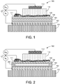
- the semiconductor device 100 operates as a memory element having enhanced hysteresis characteristics or a transistor having mitigated hysteresis characteristics, which will be discussed in further detail below.
- the semiconductor device 100 comprises the following layers: an insulating substrate 101 , a gate layer 102, a dielectric layer 104, a memory layer 106, contact pad 1 1 1 , a source layer 108, a semiconducting channel layer 1 10, and a drain layer 1 12.
- the source layer 108 is an electrically percolating layer such as, e.g.
- a dilute network of carbon nanotubes CNTs
- a layer of graphene CNTs
- a dilute network of metallic and/or semiconducting nanowires CNTs
- a layer of a conductor, semiconductor, or semi-metal including perforations CNTs
- FIG. 1 is described as including a network of carbon nanotubes as the source layer 108 (i.e. , a nanotube source layer 108)
- the other types of source layers 108 are also applicable as can be appreciated.
- the semiconductor device 100 is configured to utilize a field effect controlled Schottky barrier at the interface between the source layer 108 and the semiconducting channel layer 1 10 in order to turn the device on and off, taking advantage of the low density of states of the carbon nanotubes (or other source layer material) and their nanoscale diameters in the nanotube source layer 108.
- the memory layer 106 does not rely on charge injection from mobile carriers induced in the channel of the semiconducting channel layer 1 10. Instead, the architecture of the semiconductor device 100 enables charge injection into the memory layer 106 directly from the source layer 108 and not from the semiconducting channel layer 1 0 like other memory devices, resulting in lower write and erase voltages while preserving low reading voltages and fast reading speeds.
- the memory layer 106 may include a charge storage material or a ferroelectric material.
- the insulating substrate 101 may include an insulating material such as, but not limited to, glass or plastic that insulates the gate layer 102, which is formed on the insulating substrate 101.
- the insulating substrate 101 includes a conductive substrate (e.g., a stainless steel substrate) that includes an insulating surface layer between the conductive substrate and the gate layer 102.
- the insulating surface layer may be pre-deposited on the conductive substrate surface.
- the gate layer 102 functions as a gate electrode and includes an electrically conducting or semiconducting material.
- the material of the gate layer 102 may be an inorganic material or organic material.
- Inorganic materials include, but are not limited to, metals, semiconductors, and transparent conducting oxides.
- the gate layer 102 includes at least one kind of semiconductor such as silicon (e.g., a degeneratively-doped p-type or n-type Si substrate).
- the gate layer 102 may include a metal such as Al, Au, Ag, Pd, Pt, Ta, W, Cu, Zn, Mg, Cd, Sb, Ti, Sn, Sr, Bi, and/ or one or more of a variety of other metals as well as mixtures thereof.
- the gate layer 102 may include a transparent conducting oxide such as tin oxide, indium oxide, tin-doped indium oxide (ITO), zinc oxide, cadmium oxide, magnesium-doped indium oxide, gallium-doped indium oxide, CdSb 2 0 6 , and/or mixtures thereof.
- the transparent conducting oxide or mixtures thereof may be doped with any of the metals from the group of: Al, Au, Ag, Pd, Pt, Ta, W, Cu, Zn, Mg, Cd, Sb, Ti, Sn, Sr, and Bi, and/or one or more of a variety of other metals or mixtures thereof.
- Organic materials include, e.g., highly conductive polymer mixtures such as Poly(3,4-ethylenedioxythiophene) poly(styrenesulfonate) (PEDOT:PSS).
- the dielectric layer 104 which is formed on the gate layer 102, includes an inorganic dielectric material such as: silicon oxide, silicon nitride, silicon oxynitride (SiO x N y ), aluminum oxide, hafnium oxide, tantalum oxide, titanium oxide, lanthanum oxide, zirconium oxide, yttrium oxide, aluminum-titanium oxide, mixtures thereof, and/or one or more of a variety of organic insulating materials including, but not limited to, spin-on polymeric dielectrics such as, e.g., polyimide, polyamide, benzocyclobutene (BCB), polyethylene, or other mixtures.
- the dielectric layer 104 includes multiple layers of dielectric materials.
- the memory layer 106 includes a charge storage material that is both capable of storing charge and impervious to solvents so that the charge storage material will not dissolve during subsequent solution based processing steps during fabrication of the semiconductor device 100.
- the charge storage material of the memory layer 106 may not be impervious to solvents where the techniques used to transfer a dilute nanotube mesh does not involve a solvent (such as, e.g., PDMS stamps) and/or the semiconducting channel layer 110 is evaporated onto the source electrode 108, so that the memory layer 106 is not exposed to a solvent.
- the memory layer 106 has a thickness ranging from less than 1 nm to about 100 micrometers.
- the memory layer 106 may include a single material or may include multiple layers or a blend of different materials, such as a donor molecule blend or a nanoparticle-embedded dielectric layer, according to the claims.
- the memory layer 106 is a charge storage material including benzocyclobutene (BCB), which is a cross-linking, spin-on, low dielectric constant polymer.
- BCB may act as an electret having a charge storage ability as well as a relatively high stability.
- the BCB may be spun onto the dielectric layer 104 (such as, e.g., a Si0 2 layer) and annealed to form the memory layer 106.
- the memory layer 106 includes a charge storage material including one or more of the following: CytopTM, polystyrene (PS), poly(4-methyl styrene) (P4MS), poly(2-vinyl naphthalene) (PVN), poly(4-vinyl phenol) (PVP), poly(2-vinyl pyridine) (PVPyr) and self assembled monolayers: from the group of n-octadecylphosphonic acid, 18-phenoxyoctadecyl)trichlorosilane, docosyltrichlorosilane, hexamethyldisilazane, octadecyltrichlorosilane, poly(m-xylylene adipamide) (MXD6), poly(a-methylstyrene)(PaMS), poly(phenyl-methyl-silsequioxane) (pPMSSQ), and/or one or more of the following: Cytop
- the memory layer 106 includes a ferroelectric material that is both capable of being polarized and impervious to solvents so that the ferroelectric material will not dissolve during subsequent processing of the semiconductor device 100.
- the ferroelectric material may not be impervious to solvents where the techniques used to transfer a dilute nanotube mesh does not involve a solvent (such as, e.g., PDMS stamps) and/or the semiconducting channel layer 110 is evaporated onto the source layer 108, so that the memory layer 106 is not exposed to a solvent.
- the memory layer 106 includes a material according to claim 1 and a ferroelectric material including one or more of the following: poly(vinylidene difluoride)(PVDF) and its copolymer with trifluoroethylene(TrFE), nylon (poly-m-xylylene adipamide) and polyvinyl alcohol).
- PVDF poly(vinylidene difluoride)
- TrFE trifluoroethylene
- nylon poly-m-xylylene adipamide
- polyvinyl alcohol polyvinyl alcohol
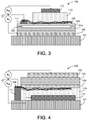
- the memory layer 106 and/or the dielectric layer 104 may include a floating gate 202 that is fully encased by a dielectric material.
- the floating gate 202 includes a layer of a conducting or semiconducting material that can store charge.
- the dielectric material covers the floating gate so that both the source layer 108 and the channel layer 110 do not make direct electrical contact with the floating gate 202.
- the floating gate 202 is made of aluminum, and the dielectric material covering it includes aluminum oxide.
- the floating gate 202 is made of silicon, and the dielectric material covering it includes silicon dioxide.
- the floating gate 202 is included in the dielectric layer 104 below the memory layer 106.
- the memory layer 106 may fully or partially include the floating gate 202.
- the dielectric material thickness is made such that charge exchange can occur between the floating gate 202 and the source layer 108, or between the floating gate 202 and the channel layer 110, via processes such as, e.g., tunneling or hot carrier injection.
- multiple layers of dielectric material may be used to control charge exchange.
- two dielectric materials 104a and 104b are used to encase the floating gate 202.
- the dielectric material 104b may form the memory layer 106.
- the memory layer 106 may not be included in the semiconductor device.
- the source layer 108 is formed on the memory layer 106. In embodiments that do not include a memory layer 106, the source layer 108 is formed on the dielectric layer 104.
- the source layer 108 may include, e.g., a percolating network of carbon nanotubes (CNTs), a layer of graphene, a percolating network of metallic and/or semiconducting nanowires, or a percolating layer of a conductor, semiconductor, or semi-metal including perforations.
- the source layer 108 is perforated to permit a subsequently deposited layer to have direct contact with both the source layer 108 and the layer on which the source layer was formed (e.g., the memory layer 106).
- the layer on which the source layer was formed e.g., the memory layer 106.
- the source layer 108 includes carbon nanotubes (CNTs) lying on their sides on the surface of the memory layer 106.
- the resulting nanotube source layer 108 has an electrically-interconnected random mesh of crossing and/or contiguous nanotubes due to the density of the nanotubes in the nanotube source layer 108.
- the mesh of the nanotube source layer 108 may be sufficiently dilute to expose at least as much of the underlying surface of the a memory layer 106 as is covered by nanotubes of the nanotube source layer 108.
- a dilute network of conducting or doped semiconducting nanowires can be used as the dilute but percolating film for the source layer 108, which is directly contacting the memory layer 106.
- nanowires include, but are not limited to, silver nanowires and silicon nanowires.
- nanotubes and semiconducting nanowires each have an intrinsic low density of states (DOS) in contrast to metals, which have a high DOS.
- the source layer 108 may be a layer of graphene or a layer of a conductor, semiconductor, or semi-metal that has been configured to have perforations.
- the source layer 108 is a dilute, and electrically percolating, layer of individualized and/or bundled nanotubes, being primarily single wall carbon nanotubes (SWNTs), and in some embodiments, preferably including mostly SWNTs.
- dilute refers to, e.g., a nanotube film included in the source layer 108 having substantial regions of the memory layer 106 not covered by nanotubes and there exist appreciable lengths of nanotubes and thin nanotube bundles that do not have other nanotubes or nanotube bundles that are associated with this layer crossing either above or below them or next to them.
- the film may include semiconducting or metallic nanowires.
- the source layer 108 may be sufficiently dilute to expose the underlying surface in the range of, e.g., about 0.1 % to about 99.9%, about 30% to about 90%, and about 50% to about 80%.
- “percolating” refers to: (i) a nanotube or nanowire source layer 108 having a density of nanotubes (i.e., number of nanotubes per unit area) or nanowires that is sufficient to provide electrical continuity from one end of the source layer 108 to the other end or (ii) a conductor, semiconductor, or semi-metal film including frequent perforations (e.g., occurring in the nanometer range, in the picometer range and/or in the micrometer range) but retaining electrical continuity from one end of the source layer 108 to the other end.
- a percolating nanotube film or network can be grown directly onto the memory layer 106 or deposited by one or more of a variety of suitable methods.
- the curved lines of the nanotube source layer 108 in the example of FIG. 1 are representative of the nanotube network (e.g. , a CNT mesh) and meant to indicate the position of the mesh with respect to the other layers.
- the curved lines in FIG. 1 are not drawn to scale or meant to physically depict how the nanotubes actually lie on the surface of the memory layer 106.
- the nanotubes lie in direct contact with portions of the surface of the memory layer 106 and contact the surface of the memory layer 106 in substantially all areas. Except for their occasional crossings where one bundle passes over another, the nanotubes of the nanotube source layer 108 lie along the surface of the memory layer 106 in FIG. 1 .
- the source layer 108 is electrically contacted by a contact pad 11 1 that, e.g., provides electrical contact to one or more edges of the nanotube network of the nanotube source layer 108.
- the contact pad 111 includes a contact material that is a metal that forms an ohmic contact with the source layer 108, e.g., with the nanotubes included in the nanotube source layer 108. Electrical contact to the source layer 108 is made via the contact pad 111 that lies along one edge of the source layer 108.
- FIG. 1 e.g. shows the contact pad 111 lying underneath the nanotube source layer 108. However, in some embodiments, the contact pad 111 is deposited on top of at least a portion of the source layer 108.
- the size of the semiconductor device 100 may be reduced (or minimized) by having each individual nanotube or nanotube bundle or nanowire in the source layer 108 directly connected to a metal electrode or contact pad 111.
- a semiconducting channel layer 110 including a semiconducting material is formed on the source layer 108.
- the semiconducting channel layer 110 is also in contact with a portion of the memory layer 106.
- the source layer 108 and semiconducting channel layer 110 form a gate voltage tunable charge injection barrier.
- the semiconductor device 100 functions as a Schottky barrier field effect transistor (FET) in which the current modulation is due to a gate-field-induced modulation of the Schottky barrier at the interface of the source layer 108 and semiconducting channel layer 110.
- FET Schottky barrier field effect transistor
- the Fermi level of the nanotubes can undergo an appreciable shift in response to a gate field and cause the barrier height to be lowered in addition to a field induced band bending that also thins the barrier to permit tunneling.
- the source layer 108 included metal instead of nanotubes, the source layer 108 would not allow a change in barrier height because metals have a high DOS that does not permit a Fermi level shift that will allow a change in barrier height.
- devices with other high DOS source materials may still work due to barrier thinning, their current modulation will not be as large as with lower DOS materials.
- Metallic nanowires although they have a larger density of states in bulk form can, have a low DOS due to quantum confinement when in nanowire form.
- the semi-metal graphene due to its lattice structure, has a low DOS.
- the semiconductor device 100 still functions in a configuration in which the source layer 108 includes a metal other than nanotubes due to field-induced band bending and tunneling.
- the local field is made very high either by the use of large gate voltages or by including a dielectric material in the dielectric layer 104 that has a very large dielectric constant, thereby severely limiting the range of materials available for the dielectric layer 104. Therefore, low density of state materials such as e.g. nanotubes provide more flexibility with respect to the selection of materials for other layers, and since nanotubes are air stable, this enhances the likelihood of commercialization of the semiconductor device 100 including nanotubes.
- the semiconducting channel layer 110 includes a semiconducting material.
- the semiconducting channel layer 110 includes an organic or inorganic semiconducting material.
- the top of the valence band of an inorganic semiconductor is equivalent to the highest occupied molecular orbital (HOMO) level of a molecular or polymeric organic semiconductor.
- the bottom of the conduction band of the inorganic semiconductor is equivalent to the lowest unoccupied molecular orbital (LUMO) level of a molecular or polymeric organic semiconductor.
- HOMO highest occupied molecular orbital
- LUMO unoccupied molecular orbital
- valence band levels and conduction band levels refer to their usual meaning for inorganic semiconductors and their equivalents for molecular and polymeric semiconductors.
- the semiconducting material of the semiconducting channel layer 110 is such that the HOMO of the semiconducting material lies within reach of the Fermi level of the nanotubes of the nanotube source layer 108 for realistically applicable gate fields induced by the gate layer 102.
- the following descriptions illustrate what happens if the semiconducting material does not lie within reach of the Fermi level of the nanotubes.
- the gate field has to generate a barrier at the accumulation layer (anti-barrier) for holes. Accordingly, the semiconductor device 100 would have a normally-on (anti-barrier) band line-up for the semiconducting channel layer 110 and the nanotube source layer 108. Additionally, when the nanotube source layer 108 includes nanotube bundles, the nanotube bundles may self screen and affect whether the channel of the semiconductor device 100 can be turned off. For example, the top nanotubes in a bundle may be screened from the gate layer 102, and the gate field of the gate layer 102 cannot switch the respective barriers off. Because those nanotubes permit current flow independent of the gate field induced by the gate layer 102, such a normally-on semiconductor device 100 cannot be turned off effectively and greatly reduces the ON/OFF current ratio.
- the gate layer 102 has to reduce the pre-existing barrier. Accordingly, the semiconductor device 100 would have a normally-off band line-up for the semiconducting channel layer 110 and the nanotube source layer 108. Further, the l DS current is switched on by the nanotubes near the bottom of the bundles of the nanotube source layer 108. Although the top nanotubes in the bundles of the nanotube source layer 108 participate little in the switching, they do not degrade the ON/OFF current ratio.
- the issues associated with being able to control the semiconductor device 100 using the gate layer 102 can be mitigated.
- the following description of semiconducting materials for the semiconducting channel layer 110 assumes that the work function of the nanotube source layer 108 is about -5.0 eV.
- Possible p-channel materials to serve as the semiconducting channel layer 110 include semiconducting materials with a HOMO level or valence band edge energy of about -5.0 eV to about -7.0 eV.
- the semiconducting material of the semiconducting channel layer 1 10 may be one or more of the following materials that has a HOMO level reasonably deeper than the work function of the nanotubes in the bundles (i.e.
- N N.N'-diil -naphthy -N.N'-diphenyl-l .r-diphenyl-l ⁇ '-diamine) NPD
- poly[(9,9-dioctyl-fluorenyl-2,7-diyl)-alt-co-(9-hexyl-3,6-carbazole)] PF-9HK
- poly(9,9-dioctyl-fluorene-co-N-(4-butylphenyl)-diphenylamine) TFB
- a semiconducting material with a HOMO level that forms an negligible hole injection barrier with the nanotube work function of about -5.0 eV may also be employed and can be chosen from one or more of the following organic or inorganic semiconducting materials with a HOMO level or valence band edge energy of about -5.0 eV to about -5.2 eV: polycrystalline silicon, pentacene, poly (3-hexylthiophene) (P3HT), rubrene, and tetracene.
- the valence band edge or HOMO level of the semiconducting channel layer 1 10 is within a range of about -1.5 eV to about +1 .5 eV of the work function of the source layer 108.
- possible materials included in the semiconducting channel layer include semiconducting materials with a LUMO level or conduction band edge energy of about -3.0 eV to about -5.0 eV.
- the use of a semiconducting channel layer 110 with a LUMO level forming a normally off band line-up with the nanotube source layer 108 (i.e., an electron injection barrier) with said LUMO level of about -3.0 eV to about -4.8 eV (when the work function of the nanotubes is about -5.0eV) permits transistor action gating the electron current.
- Applicable materials for the semiconducting channel layer 110 include: 5,5_-diperfluorohexylcarbonyl-2,2_:5_,2_:5_,2_-quaterthiophene (DFHCO-4T), DFH-4T, DFCO-4T, P(NDI20D-T2), PDI8-CN2, PDIF-CN2, F16CuPc and fullerene, naphthalene, perylene, and oligothiophene derivatives.
- DFHCO-4T 5,5_-diperfluorohexylcarbonyl-2,2_:5_,2_:5_,2_-quaterthiophene
- DFH-4T 5,5_-diperfluorohexylcarbonyl-2,2_:5_,2_:5_,2_-quaterthiophene
- DFH-4T 5,5_-diperfluorohexylcarbonyl-2,2_:5_,2
- a semiconducting material with a LUMO level that forms a negligible electron injection barrier with the nanotube work function of about -5.0 eV may also be employed and can be any organic or inorganic semiconductor with a LUMO level or conduction band edge energy of about -4.8 eV to about -5.0 eV.
- the conduction band edge or LUMO level of the semiconducting channel layer 110 is within a range of about -1.5 eV to about +1.5 eV of the work function of the source layer 108.
- the semiconducting channel layer 110 can also include semiconducting materials that form a negligible injection barrier with the nanotubes. Negligible means that the offset between the nanotube work function and either the HOMO or LUMO level of the semiconducting channel layer 110 is less than about 0.2 eV. This is because individualized nanotubes have a smaller diameter than bundled nanotubes and are not expected to suffer from the screening mechanism previously described, thereby allowing a charge injection barrier to be created through application of a gate field to turn the device off.
- the semiconducting channel layer 110 may include an organic semiconducting material is formed on the source layer 108.
- the organic semiconducting material of the semiconducting channel layer 110 can include a linearly condensed polycyclic aromatic compound (or acene compound) such as, e.g., naphthalene, anthracene, rubrene, tetracene, pentacene, hexacene, and derivatives thereof; a pigment such as, e.g., copper-phthalocyanine(CuPc)-based compounds, azo compounds, perylene-based compounds, and derivatives thereof; a low-molecular compound such as, e.g., hydrazone compounds, triphenyl methane-based compounds, diphenylmethane-based compounds, stilbene-based compounds, arylvinyl compounds, pyrazoline-based compounds, triphenyl amine derivatives (TPD), arylamine compounds, low-molecular weight aryl
- the drain layer 1 12 is formed on the semiconducting channel layer 110, and the drain layer 112 includes a conducting material.
- the drain layer 112 may include a layer of carbon nanotubes, a contiguous metallic film, a contiguous semiconducting film, a contiguous transparent conducting oxide, or a layer of semiconducting nanowires.
- the drain layer 112 includes a thin Pd metallization deposited directly on top of the semiconducting channel layer 110.
- the drain layer 112 may include a metal such as, e.g., gold.
- the drain layer may include a layer of nanotubes.
- the size of the semiconductor device 100 may be reduced (or minimized) by utilizing an individual nanotube in the drain layer 1 12, with the nanotube connected to a metal electrode.
- the device arrangement described herein can be embodied as a transparent semiconductor device 100.
- the gate layer 102 can be a conducting material that is optically transparent, such as indium tin oxide, or a thin SWNT film that is deposited onto a transparent insulating substrate 101.
- the transparent gate layer 102 can then be covered by an optically transparent dielectric layer 104 followed by an optically transparent memory layer 106, followed by the dilute, percolating, source layer 108 followed by the rest of the device layers as mentioned.
- a transparent conducting material can also be used for the drain layer 112, such as a thin nanotube film or bi-layer of a thin metal followed by a transparent conducting oxide layer.
- the insulating substrate 101 , gate layer 102, the dielectric layer 104, the memory layer 106, the source layer 108, the semiconducting channel layer 110, and the drain layer 112 are all optically transparent.
- the configuration described is also amenable to the fabrication of flexible transistors requiring that SWNT films be used for the source, drain and gate layers with a flexible dielectric layer 104, a flexible memory layer 106, constructed on a flexible insulating substrate 101.
- the insulating substrate 101 , gate layer 102, the dielectric layer 104, the memory layer 106, the source layer 108, the semiconducting channel layer 1 10, and the drain layer 112 are all flexible.
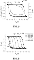
- the top-gated semiconductor device 400 comprises the following layers: an insulating substrate 101 , a gate layer 102, a dielectric layer 104, a memory layer 106, contact pad 111 , a source layer 108, a semiconducting channel layer 110, and a drain layer 112.
- the insulating substrate 101 insulates the drain layer 112, which is formed on the insulating substrate 101.
- a semiconducting channel layer 110 including a semiconducting material is formed on the drain layer 112.
- the source layer 108 is formed on the semiconducting channel layer 110.
- the source layer 108 is perforated to permit a subsequently deposited layer to have direct contact with both the source layer 108 and the layer on which the source layer was formed. At least a portion of the source layer 108 is in contact with the contact pad 111.
- a memory layer 106 is formed over the source layer 108 in contact with it and in contact with the semiconducting channel layer 110.
- the dielectric layer 104 is formed on the memory layer 106 and the gate layer 102 is formed on the dielectric layer 104.
- source layer 108 including each individual nanotube or nanotube bundle directly contacted by metal electrodes is used to reduce or minimize the size of the semiconductor device 400.
- a cyclic transfer curve 500 for an embodiment of the semiconductor device 100 depicted in FIG. 1 comprising a gate layer 102 that includes degeneratively doped p-type Si, a memory layer 106 that includes BCB, a nanotube source layer 108 including a carbon nanotube dilute network, a contact pad 111 including palladium, a semiconducting channel layer 110 that includes poly(9,9-dioctyl-fluorene-co-N-(4-butylphenyl)-diphenylamine) (TFB), and a drain layer 112 that includes gold.
- TFB poly(9,9-dioctyl-fluorene-co-N-(4-butylphenyl)-diphenylamine)
- the ON/OFF ratio between the drain current (l D ) 502 in the ON-state and l D 504 in the OFF-state of the semiconductor device 100 ( FIG. 1 ) is more than 4 orders of magnitude.
- the ON-state current 502 is about 0.8 ⁇ A for about a 0.035 mm 2 pixel size, corresponding to a current density of about 2.3 mA/cm 2 .
- injection into the semiconducting channel layer 1 10 ( FIG. 1 ) occurs over the entire overlap area between the nanotube source layer 108 ( FIG. 1 ) and the drain layer 112 ( FIG. 1 ) so that an areal current density is sensibly defined, just as for organic light emitting diodes and organic solar cells.
- the low driving voltage of the semiconductor device 100 is an improvement over organic thin film transistors.
- submicron particulates in the nanotube source material limited how thin the semiconducting channel layer 110 could be made before direct shorts between the nanotube source layer 108 and drain layer 112, respectively, rendered the devices inoperable.
- the semiconducting channel layer 110 of at least 350 nm in thickness of this embodiment avoided such direct shorts.
- the thickness of the semiconducting channel layer 110 may be as small as about 1-2 nm.
- the semiconducting channel layer 110 thickness can be in a range of, e.g., about 1 nm to about 5000 nm. Note that for a lateral organic FET, a 350 nm channel length would require expensive high resolution patterning.
- the semiconducting channel layer 110 can be made thinner, allowing still higher current densities to be realized, which will benefit device operation because of low ON-state channel resistance (as indicated by the ability to drive higher currents) thereby improving the reading speed and reducing the power consumption of the semiconductor device 100.
- a hysteresis of about 157 V is shown for a gate voltage scan of -100V to +100V.
- Large hysteresis is useful for non-volatile memory applications.
- the large gate voltages used here are due to dielectric layer 104 ( FIG. 1 ), which includes a thermal oxide having a thickness of about 200 nm to avoid gate leakage currents.
- the gate voltage required should be greatly reduced by reduction of the thickness of the dielectric layer 104, without compromising the memory characteristics.
- BCB was designed as a charge storage layer to serve as the memory layer 106 ( FIG. 1 ).
- BCB was selected because it is commercially available, easy to process and stable after curing.
- the direction of the cyclic transfer curves indicates the origin of the hysteresis.
- an anticlockwise or lower back sweep current (lower BSC) hysteresis is generated by charge storage in dielectrics near the channel. Indeed, strong lower BSC hysteresis can be seen in the cyclic transfer curves of the semiconductor devices, indicating that charge storage is the origin of the hysteresis.
- FIG. 6 A trend shown in FIG. 6 is a shift of threshold voltages that follow the "turn back point" gate voltage in the scan.
- the shift mechanism can be understood on the basis of electrostatics as follows. Suppose, without loss of generality, that V G is at its most negative value. In order to balance the negative charge accumulated on the gate layer 102 ( FIG. 1 ), both the nanotube source layer 108 ( FIG. 1 ) and the memory layer 106 ( FIG. 1 ) contain a compensating amount of positive charge.
- the positive charge on the carbon nanotubes of the source layer 108 depresses the contact barrier with the semiconducting channel layer 110 ( FIG. 1 ) allowing for hole injection so that the p-channel device is in its ON-state. Now scan the gate voltage towards zero, but only to about -50 V (curve 602 in FIG. 6 ). In response to the decreasing V G the negative charge on the gate layer 102 and the corresponding positive charge on the combination of the nanotube source layer 108 and memory layer 106 is reduced, but the charge on the memory layer 106 is trapped and less easily drained.
- the positive charge on the carbon nanotubes of the nanotube source layer 108 is preferentially drained, raising their contact barrier with the semiconducting channel layer 110, resulting in the rapid turn off of the channel.
- the first turn back point 50 V
- V G becomes more negative again
- the positive charge in the nanotube source layer 108 is quickly replenished rapidly turning the channel back on again. If V G is returned to about -100 V in each excursion, this behavior occurs for any turn back point so that the apparent threshold voltage at which the channel turns on shifts to lie near the V G where the scan changes direction and turns back.
- the memory layer 106 can store negative charge as well as positive charge so this behavior holds for both negative and positive V G turnback points. Symmetric behaviors are also shown, by the cyclic transfer curves 700 of FIG. 7 , for V G scans that always return to +100V. There the apparent threshold voltages at which the channel turns off shifts to lie near the turn back point. The hysteresis in the semiconductor device 100 is thus fully programmable, depending on the V G turn back points and can even be made effectively zero by restricting the scan range as illustrated by the cyclic transfer curves 800 of FIG. 8 .
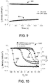
- FIG. 9 shows the stability of the semiconductor device 100 ( FIG. 1 ) for both ON and OFF states, respectively.
- V G was scanned to 100 V, and then scanned back to 0 V.
- the OFF-state was set by scanning V G to -100 V first and back to 0 V.
- the ON-state source-drain current 902 was still more than 3 orders of magnitude higher than the OFF-state l D 904, indicating relatively good charge storage stability of the BCB layer.
- BCB is not typically used as a charge storage material. Charge relaxation leads to charge loss in the memory layer 106 ( FIG.
- a more stable semiconductor device 100 is possible with the use of a charge storage material that exhibits a greater barrier to charge exchange with the CNTs.
- the material included in the memory layer 106 to serve as a charge storage layer is a material that exhibits an energy barrier to charge exchange with the nanotube source layer 108. Overcoming that barrier and transferring charge into (or out of) the memory layer 106 involves a characteristic minimum change in the gate voltage V G that is referred to as the critical threshold voltage, AV C .
- This critical threshold voltage AV C is independent of the charge already stored in the charge storage layer 106 and independent of the sign of the stored charge.
- the quantity of charge in the memory layer 106 is Q 0 .
- Increasing the quantity of charge Q in the memory layer 106 to Q 0 +AQ involves a corresponding minimum change in the gate voltage V G of AV C , resulting in a new value of the gate voltage V G of V G0 +AV C .
- a return of the gate voltage V G to the given gate voltage V G0 does not correspondingly return the quantity of charge Q in the memory layer 106 to Q 0 . Rather, returning the quantity of charge Q in the memory layer 106 to Q 0 requires that the gate voltage V G be reduced to V G0 -AV C .
- the charge state of the memory layer 106 does not change.
- the semiconductor device 100 when used as a memory element, relies on hysteresis to define a plurality of memory states, and the hysteresis in turn requires distinct charge states of the memory layer 106, the quantity ⁇ AV C , which is a characteristic of the charge storage material used (as well as the dielectric layer 104 material and thickness and memory layer 106 thicknesses), sets the lower limit for the write and erase voltages for the semiconductor device 100, when used as a memory element.
- the semiconductor device 100 is operated as a transistor instead of a memory element.
- hysteresis is undesirable.
- carbon nanotube vertical field effect transistors (CN-VFETs) (without the memory layer 106) generally exhibit substantial hysteresis.
- the memory layer 106 of the semiconductor device 100 helps mitigate hysteresis effects normally observed without the memory layer 106 when the semiconductor device 100 is operated as a transistor so long as the range of gate voltage is limited to be less than ⁇ AV C .
- the curves 800 demonstrate that the hysteresis is near zero with the inclusion of BCB in the memory layer 106 ( FIG. 1 ) while limiting the range of gate voltages applied to the semiconductor device 100 ( FIG. 1 ).
- the gate voltage range is limited to a span of about ⁇ 25 V (i.e., the range ⁇ AV C is about 25V, under these conditions)
- the gate voltage range is limited to a span of about ⁇ 25 V (i.e., the range ⁇ AV C is about 25V, under these conditions)
- the hysteresis that is observed when the semiconductor device 100 is operated as a memory element is mitigated when the semiconductor device 100 is operated as a transistor in a limited gate voltage span.
- this nearly hysteresis-free operation can be programmed to occur about any desired gate voltage by the initial gate voltages (about >25 V) applied to the semiconductor device 100 as demonstrated by the shifted curves 800 in FIG. 8 .
- the limited gate voltage range that permits nearly hysteresis-free operation in the semiconductor device 100 also however limits the ratio of the ON current to the OFF current in the device. Large ON/OFF current ratios are desirable in transistors, and so for this purpose memory layers that have larger ⁇ AV C to permit larger voltage swings and thereby go further on and off (increasing their ON/OFF ratio) are desirable.
- the charge storage layer 106 is such that charge exchange between the source layer 108 and the charge storage layer 106 only occurs if the gate voltage exceeds a critical threshold gate voltage, thereby operating as a hysteresis-free transistor with a programmable threshold voltage.
- the deleterious hysteresis in CN-VFETs arises because of charge traps in a dielectric layer 104 (e.g., silicon oxides and nitrides). These charge traps can also store charge and thereby induce hysteresis in the devices.
- a dielectric layer 104 e.g., silicon oxides and nitrides.
- these charge traps can also store charge and thereby induce hysteresis in the devices.
- the barrier to charge exchange with the dielectrics is variable, and small, leading to a small effective ⁇ AV C .
- FIG. 10 shown is a comparison of the cyclic transfer curves 1000 of a memory element including a BCB charge storage layer 106 (corresponding to curve 1002) and two control CN-VFETs without a charge storage layer. All devices were built on a p-Si substrate with a 200 nm thick thermal oxide layer. The first control device (corresponding to curve 1004) was built on the untreated Si02 dielectric layer. For the second control device (corresponding to curve 1006), the oxide surface was treated by a commercially available water repellent (Rain X) to render the oxide surface hydrophobic. All other parameters for the three devices were identical.
- the hysteresis for the memory element was about 157 V, while the hysteresis for the control devices (without BCB) is about 98 V and about 64 V (curves 1004 and 1006), respectively.
- the hysteresis in the control devices (curves 1004 and 1006) is offset because Si0 2 is dominated by electron traps as opposed to BCB which traps holes with apparently equal efficiency.
- FIG. 1 1 illustrated is a method of fabricating a semiconductor device 100 ( FIG. 1 ) according to various embodiments of the present disclosure. It is understood that the flowchart 1 100 of FIG. 1 1 provides merely an example of the many different steps that may be employed to implement the fabrication of a semiconductor device 100 as described herein.
- a gate layer 102 FIG. 1
- a dielectric layer 104 FIG. 1
- a memory layer 106 FIG. 1
- FIG. 1 is formed on the dielectric layer 104.
- the memory layer 106 may include a self-assembled molecular monolayer according to the claims, a polymer according to the claims deposited through a liquid solution, or a polymer according to the claims deposited through a liquid solution with embedded nanoparticles.
- a floating gate 202 FIG. 2 is included in the dielectric layer 104 and/or memory layer 106.
- a source layer 108 ( FIG. 1 ) is formed on the memory layer 106.
- the source layer 108 may be, e.g., an electrically percolating network of carbon nanotube(s), a layer of graphene, an electrically percolating network of one or more metallic and/or semiconducting nanowire(s), or an electrically percolating layer of a conductor, semiconductor, or semi-metal that has been configured to have perforations, by a process such as, but not limited to, evaporation through a photolithographically defined mask or a mask defined by self assembled nanoparticles, deposition of a continuous film followed by masking and etching, etching to be performed by solution chemistry or by reactive species (e.g.
- a nanotube source layer 108 includes at least one nanotube.
- the source layer 108 is perforated to permit a subsequently deposited layer to have direct contact with both the source layer 108 and the layer on which the source layer was formed (e.g. , the memory layer 106).
- a contact pad 1 1 1 ( FIG. 1 ) is formed in contact with at least a portion of the source layer 108.
- the contact pad 11 1 may be formed on at least a portion of a nanotube source layer 108.
- electrical contact to the nanotube source layer 108 is formed by depositing the contact pad 1 11 on the memory layer 106 prior to forming the nanotube source layer 108.
- a semiconducting channel layer ( FIG. 1 ) is formed on another portion of the source layer 108 such that the semiconducting channel layer 1 10 is in contact with both the source layer 108 and the memory layer 106.
- the thickness of the semiconducting channel layer 1 10 (i.e. , the channel length of the semiconductor device 100) is determined by the processing parameters in the method of depositing the semiconducting channel layer 1 10, such as spin-coating, thermal evaporation, and/or one or more of a variety of other thin film deposition techniques.
- the semiconducting channel layer 110 is formed on the source layer 108 by a thin film deposition technique such as resistive thermal evaporation, sputtering, spin-coating, ink-jet printing, vapor-jet printing, drop-casting, electrochemical deposition or other means that may provide fine control over the channel layer thickness.
- the semiconducting channel layer 110 is as thin as a single molecular layer (e.g. about 1 nm) or hundreds of nanometers thick (e.g. , about 500 nm) or more, or one of a variety of thicknesses in between, with thickness control provided by the deposition parameters.
- the thickness of the semiconducting channel layer coating the source layer 108 defines the channel length of the semiconductor device 100.
- the substrate can be heated during the deposition to enhance the crystallinity of the semiconducting channel layer 110 or kept at room temperature to attain an amorphous phase.
- the deposition parameters can be modified to increase the amorphous phase percent of the channel layer such as by increasing the growth rate during a resistive thermal evaporative type of deposition method. It should be noted that due to the vertical architecture of the device, in some embodiments an amorphous channel layer is preferred to prevent shorting paths through grain boundaries. If an amorphous phase cannot be attained at room temperature conditions and high growth rates, then the smaller crystallite size of the films versus films grown at higher temperatures and slower growth rates should permit a more "amorphous like" film and bring with it the benefits of an amorphous film.
- the semiconductor device 100 can be subjected to a post evaporation heating cycle to improve the crystallinity of the semiconducting channel layer 110 if it deemed necessary.
- a drain layer 112 ( FIG. 1 ) is formed on the semiconducting channel layer 110.
- the drain layer 112 may be, e.g., a layer of one or more carbon nanotube(s), a contiguous metallic film, a contiguous semiconducting film, a contiguous transparent conducting oxide, or a layer of one or more semiconducting nanowire(s).
- FIG. 11 shows a specific order of execution, it is understood that the order of execution may differ from that which is depicted. For example, the order of execution of two or more blocks may be scrambled relative to the order shown. Also, two or more blocks shown in succession in FIG. 1 1 may be executed concurrently or with partial concurrence. Further, in some embodiments, one or more of the blocks shown in FIG. 11 may be skipped or omitted.
- a drain layer 112 is formed on a substrate 101 and a semiconducting channel layer 110 is formed on the drain layer 112.
- a source layer 108 is formed on the semiconducting channel layer 110 with at least a portion of the source layer 108 in contact with a contact pad 111.
- a memory layer 106 is formed on the source layer 108 and in contact with the semiconducting channel layer 110.
- the dielectric layer 104 is formed on the memory layer 106 and the gate layer 102 is formed on the dielectric layer 104.
- the nanotubes making up the nanotube source layer 108 provide for a natural gate field enhancement that facilitates charge exchange with the memory layer 106 (when the memory layer 106 includes a charge storage material) at comparatively low gate voltages. Additionally, the majority of charge exchange with the charge storage material is directly from the nanotube source layer 108 rather than being mediated through the semiconducting channel layer 110. This means that the band structure properties of the charge storage material of the memory layer 106 are optimized against the nanotubes independent of the semiconducting material used for the semiconducting channel layer 110.
- the vertical channel architecture and distinct operational mode of the semiconductor device 100 eliminates the coupling between mobility and the roughness of the dielectric layer. Further, the vertical channel architecture allows a higher packing density of integrated circuit (IC) and/or memory chips in contrast to a lateral channel architecture which has a lower density and/or the additional expense of high resolution patterning.
- both a high mobility of carriers and an efficient (low gate voltage) charge injection into the memory layer 106 may be possible.
- High mobility enables a reduction in ON-state channel resistance for high speed reading of a memory.
- the ability to inject charges efficiently into a memory layer 106 enables the realization of low write and erase voltages for the memory.
- the semiconductor device 100 has a higher read speed and lower write and erase voltages.
- the charges induced by the gate electric field forming the conducting channel accumulate within the first few nanometers of the interface of the gate dielectric and the semiconducting film in the direction perpendicular with the plane of the interface. If the interface is rough (i.e., on the order of several or tens of nanometer RMS roughness or larger), the carrier mobility in this ultra thin conducting channel is greatly reduced- by orders of magnitude. Given that the available organic materials for OTFTs are already low in mobility, it becomes untenable to further compromise the mobility by roughening the interface with the charge storage layer to reduce write and erase voltages.
Applications Claiming Priority (2)
| Application Number | Priority Date | Filing Date | Title |
|---|---|---|---|
| US31034210P | 2010-03-04 | 2010-03-04 | |
| PCT/US2011/027155 WO2011109693A2 (en) | 2010-03-04 | 2011-03-04 | Semiconductor devices including an electrically percolating source layer and methods of fabricating the same |
Publications (3)
| Publication Number | Publication Date |
|---|---|
| EP2543086A2 EP2543086A2 (en) | 2013-01-09 |
| EP2543086A4 EP2543086A4 (en) | 2014-04-23 |
| EP2543086B1 true EP2543086B1 (en) | 2019-06-19 |
Family
ID=44542847
Family Applications (1)
| Application Number | Title | Priority Date | Filing Date |
|---|---|---|---|
| EP11751409.1A Active EP2543086B1 (en) | 2010-03-04 | 2011-03-04 | Semiconductor devices including an electrically percolating source layer and methods of fabricating the same |
Country Status (11)
| Country | Link |
|---|---|
| US (1) | US8952361B2 (pt) |
| EP (1) | EP2543086B1 (pt) |
| JP (1) | JP5810103B2 (pt) |
| KR (1) | KR101860958B1 (pt) |
| CN (1) | CN102823009B (pt) |
| AU (1) | AU2011222601B2 (pt) |
| BR (1) | BR112012022290A2 (pt) |
| CA (1) | CA2791625A1 (pt) |
| RU (1) | RU2012142197A (pt) |
| SG (1) | SG183900A1 (pt) |
| WO (1) | WO2011109693A2 (pt) |
Families Citing this family (37)
| Publication number | Priority date | Publication date | Assignee | Title |
|---|---|---|---|---|
| US9214644B2 (en) | 2010-12-07 | 2015-12-15 | University Of Florida Research Foundation, Inc. | Active matrix dilute source enabled vertical organic light emitting transistor |
| CN102646592B (zh) * | 2011-05-03 | 2014-12-03 | 京东方科技集团股份有限公司 | 薄膜场效应晶体管器件及其制备方法 |
| US8791450B2 (en) | 2011-09-22 | 2014-07-29 | Sensor Electronic Technology, Inc. | Deep ultraviolet light emitting diode |
| US9705032B2 (en) | 2011-09-22 | 2017-07-11 | Sensor Electronic Technology, Inc. | Deep ultraviolet light emitting diode |
| US9530975B2 (en) * | 2012-09-24 | 2016-12-27 | Wake Forest University | Method of making an organic thin film transistor |
| KR102084288B1 (ko) | 2012-11-05 | 2020-03-03 | 유니버시티 오브 플로리다 리서치 파운데이션, 아이엔씨. | 디스플레이의 휘도 보상 |
| KR102010113B1 (ko) * | 2012-11-30 | 2019-08-12 | 유니버시티 오브 플로리다 리서치 파운데이션, 아이엔씨. | 양극성 수직 전계 효과 트랜지스터 |
| US8941095B2 (en) | 2012-12-06 | 2015-01-27 | Hrl Laboratories, Llc | Methods for integrating and forming optically transparent devices on surfaces |
| CN103227204B (zh) * | 2013-04-01 | 2015-07-08 | 南京邮电大学 | 晕掺杂的双材料异质栅石墨烯条带场效应管 |
| KR102116978B1 (ko) * | 2013-10-07 | 2020-05-29 | 삼성전자 주식회사 | 그래핀 소자 및 그 제조 방법 |
| KR102065110B1 (ko) * | 2013-11-12 | 2020-02-11 | 삼성전자주식회사 | 플렉서블 그래핀 스위칭 소자 |
| JP2017521849A (ja) * | 2014-04-24 | 2017-08-03 | ユニバーシティ オブ フロリダ リサーチ ファンデーション インコーポレーティッド | 高パワーエレクトロニクスのための可変バリアトランジスタ |
| CN104062775B (zh) * | 2014-06-30 | 2017-02-15 | 浙江大学 | 非挥发性的光学记忆单元 |
| KR102237826B1 (ko) * | 2014-07-18 | 2021-04-08 | 삼성전자주식회사 | 그래핀 소자와 그 제조 및 동작방법과 그래핀 소자를 포함하는 전자장치 |
| FR3027155B1 (fr) * | 2014-10-08 | 2018-01-12 | Ecole Polytechnique | Procede de fabrication d'un dispositif electronique, en particulier a base de nanotubes de carbone |
| KR101938934B1 (ko) * | 2016-03-02 | 2019-04-10 | 광주과학기술원 | 이득조절이 가능한 그래핀-반도체 쇼트키 접합 광전소자 |
| CN105823972B (zh) * | 2016-03-15 | 2018-07-27 | 南京邮电大学 | 一种有机场效应晶体管存储器最小存储深度的计算方法 |
| US20180175209A1 (en) * | 2016-12-20 | 2018-06-21 | Globalfoundries Inc. | Semiconductor structure including one or more nonvolatile memory cells and method for the formation thereof |
| CN106953010A (zh) * | 2017-03-07 | 2017-07-14 | 南京邮电大学 | 一种基于聚合物掺杂半导体纳米粒子的有机场效应晶体管存储器 |
| US10475514B2 (en) * | 2017-05-11 | 2019-11-12 | The Penn State Research Foundation | Nonvolatile digital computing with ferroelectric FET |
| CN108376740B (zh) * | 2018-01-18 | 2022-03-29 | 上海集成电路研发中心有限公司 | 复合沟道晶体管及其制备方法 |
| CN110364621B (zh) * | 2018-04-11 | 2023-12-01 | 清华大学 | 一种触觉存储电子器件及电子设备 |
| CN109036487B (zh) * | 2018-07-20 | 2021-03-02 | 福州大学 | 一种基于短沟道有机晶体管的多级光存储器及其制备方法 |
| CN109192750B (zh) * | 2018-07-23 | 2021-06-22 | 华南师范大学 | 低压高速擦写的柔性有机非易失性存储器件及其制备方法 |
| CN109037441B (zh) * | 2018-08-01 | 2022-06-21 | 苏州大学 | 半导体电存储材料及其制备的柔性电存储器件及制备方法 |
| CN109037355B (zh) * | 2018-08-27 | 2020-04-10 | 湘潭大学 | 一种基于铁电栅调控的肖特基二极管及其制备方法 |
| JP7297280B2 (ja) | 2018-08-29 | 2023-06-26 | 国立大学法人千葉大学 | 振動発電器及びエレクトレット |
| CN110911409B (zh) * | 2018-09-18 | 2022-05-03 | 联华电子股份有限公司 | 非挥发性存储器及其形成方法 |
| CN109411543A (zh) * | 2018-09-20 | 2019-03-01 | 华南理工大学 | 一种透明薄膜晶体管及其制备方法 |
| KR102111526B1 (ko) * | 2018-10-19 | 2020-06-04 | 성균관대학교산학협력단 | 셀렉터 포함 메모리 소자 |
| CN109411605A (zh) * | 2018-10-26 | 2019-03-01 | 福州大学 | 一种铁电存储器及其制备方法 |
| CN109755255A (zh) * | 2019-01-24 | 2019-05-14 | 福州大学 | 一种金属氧化物存储器及其制备方法 |
| WO2020218420A1 (en) | 2019-04-26 | 2020-10-29 | Jsr Corporation | Method of driving a light emitting display and display |
| CN110818711A (zh) * | 2019-11-01 | 2020-02-21 | 河北科技大学 | 一种有机异质结纳米线的制备方法 |
| CN111211222A (zh) * | 2020-02-19 | 2020-05-29 | 国家纳米科学中心 | 一种有机薄膜晶体管的用途及基于其的有机薄膜的杨氏模量值评估方法 |
| CN113517403B (zh) * | 2021-07-26 | 2024-02-27 | 南京信息工程大学滨江学院 | 一种新型的有机pn异质结液相的生长方法 |
| CN113921616A (zh) * | 2021-08-27 | 2022-01-11 | 华南师范大学 | 一种低压驱动喷墨打印柔性突触晶体管及其制备方法 |
Citations (2)
| Publication number | Priority date | Publication date | Assignee | Title |
|---|---|---|---|---|
| US20020195644A1 (en) * | 2001-06-08 | 2002-12-26 | Ananth Dodabalapur | Organic polarizable gate transistor apparatus and method |
| US20080157128A1 (en) * | 2006-09-14 | 2008-07-03 | Johns Hopkins University | Methods for producing multiple distinct transistors from a single semiconductor |
Family Cites Families (15)
| Publication number | Priority date | Publication date | Assignee | Title |
|---|---|---|---|---|
| JPS5532235B1 (pt) * | 1977-05-18 | 1980-08-23 | ||
| US5742075A (en) * | 1994-10-07 | 1998-04-21 | Iowa State University Research Foundation, Inc. | Amorphous silicon on insulator VLSI circuit structures |
| JP4247377B2 (ja) * | 2001-12-28 | 2009-04-02 | 独立行政法人産業技術総合研究所 | 薄膜トランジスタ及びその製造方法 |
| CN100385677C (zh) * | 2002-08-07 | 2008-04-30 | 皇家飞利浦电子股份有限公司 | 绝缘栅晶体管、晶体管电路、晶体管装置及晶体管的操作方法 |
| KR100508545B1 (ko) | 2002-12-14 | 2005-08-17 | 한국전자통신연구원 | 수직 구조의 반도체 박막 트랜지스터 |
| US7095075B2 (en) * | 2003-07-01 | 2006-08-22 | Micron Technology, Inc. | Apparatus and method for split transistor memory having improved endurance |
| EP1508926A1 (en) * | 2003-08-19 | 2005-02-23 | Hitachi, Ltd. | Nanotube transistor device |
| JP4420692B2 (ja) * | 2004-02-10 | 2010-02-24 | シャープ株式会社 | メモリ素子の製造方法 |
| KR100682925B1 (ko) * | 2005-01-26 | 2007-02-15 | 삼성전자주식회사 | 멀티비트 비휘발성 메모리 소자 및 그 동작 방법 |
| JP2007109454A (ja) * | 2005-10-12 | 2007-04-26 | Toyota Motor Corp | リチウム二次電池およびその製造方法 |
| US7439594B2 (en) * | 2006-03-16 | 2008-10-21 | Micron Technology, Inc. | Stacked non-volatile memory with silicon carbide-based amorphous silicon thin film transistors |
| KR100680001B1 (ko) * | 2006-04-05 | 2007-02-08 | 광주과학기술원 | 고분자 전하 저장층을 이용한 유기 전계효과 트랜지스터기반 비휘발성 유기물 트랜지스터 메모리 및 그 제조방법 |
| WO2009036071A2 (en) * | 2007-09-10 | 2009-03-19 | University Of Florida Research Foundation, Inc. | Nanotube enabled, gate-voltage controlled light emitting diodes |
| WO2008008648A2 (en) * | 2006-06-29 | 2008-01-17 | University Of Florida Research Foundation, Inc. | Short channel vertical fets |
| KR100866751B1 (ko) * | 2006-12-27 | 2008-11-03 | 주식회사 하이닉스반도체 | 강유전체 소자를 적용한 반도체 메모리 장치 및 그리프레쉬 방법 |
-
2011
- 2011-03-04 RU RU2012142197/28A patent/RU2012142197A/ru not_active Application Discontinuation
- 2011-03-04 CN CN201180011714.7A patent/CN102823009B/zh active Active
- 2011-03-04 CA CA2791625A patent/CA2791625A1/en not_active Abandoned
- 2011-03-04 WO PCT/US2011/027155 patent/WO2011109693A2/en active Application Filing
- 2011-03-04 US US13/580,199 patent/US8952361B2/en active Active
- 2011-03-04 EP EP11751409.1A patent/EP2543086B1/en active Active
- 2011-03-04 KR KR1020127025507A patent/KR101860958B1/ko active IP Right Grant
- 2011-03-04 BR BR112012022290A patent/BR112012022290A2/pt not_active IP Right Cessation
- 2011-03-04 AU AU2011222601A patent/AU2011222601B2/en not_active Ceased
- 2011-03-04 JP JP2012556259A patent/JP5810103B2/ja active Active
- 2011-03-04 SG SG2012065504A patent/SG183900A1/en unknown
Patent Citations (2)
| Publication number | Priority date | Publication date | Assignee | Title |
|---|---|---|---|---|
| US20020195644A1 (en) * | 2001-06-08 | 2002-12-26 | Ananth Dodabalapur | Organic polarizable gate transistor apparatus and method |
| US20080157128A1 (en) * | 2006-09-14 | 2008-07-03 | Johns Hopkins University | Methods for producing multiple distinct transistors from a single semiconductor |
Non-Patent Citations (1)
| Title |
|---|
| XU ZHENG ET AL: "Vertical organic light emitting transistor", APPLIED PHYSICS LETTERS, A I P PUBLISHING LLC, US, vol. 91, no. 9, 30 August 2007 (2007-08-30), pages 92911 - 92911, XP012100914, ISSN: 0003-6951, DOI: 10.1063/1.2778751 * |
Also Published As
| Publication number | Publication date |
|---|---|
| EP2543086A2 (en) | 2013-01-09 |
| RU2012142197A (ru) | 2014-04-10 |
| CA2791625A1 (en) | 2011-09-09 |
| US20120319096A1 (en) | 2012-12-20 |
| CN102823009A (zh) | 2012-12-12 |
| JP2013521664A (ja) | 2013-06-10 |
| KR101860958B1 (ko) | 2018-05-24 |
| WO2011109693A2 (en) | 2011-09-09 |
| AU2011222601A1 (en) | 2012-09-06 |
| US8952361B2 (en) | 2015-02-10 |
| WO2011109693A3 (en) | 2011-12-29 |
| BR112012022290A2 (pt) | 2018-05-15 |
| JP5810103B2 (ja) | 2015-11-11 |
| SG183900A1 (en) | 2012-10-30 |
| CN102823009B (zh) | 2015-09-16 |
| AU2011222601B2 (en) | 2013-09-26 |
| EP2543086A4 (en) | 2014-04-23 |
| KR20130014527A (ko) | 2013-02-07 |
Similar Documents
| Publication | Publication Date | Title |
|---|---|---|
| EP2543086B1 (en) | Semiconductor devices including an electrically percolating source layer and methods of fabricating the same | |
| US8217386B2 (en) | Short channel vertical FETs | |
| EP2926376B1 (en) | Ambipolar vertical field effect transistor | |
| Lee et al. | n‐Type doped conjugated polymer for nonvolatile memory | |
| Asadi et al. | Organic non-volatile memories from ferroelectric phase-separated blends | |
| Liu et al. | Memory effect of a polymer thin-film transistor with self-assembled gold nanoparticles in the gate dielectric | |
| US7858978B2 (en) | Nonvolatile organic bistable memory device and method of manufacturing the same | |
| JP2004006476A (ja) | 縦型有機トランジスタ | |
| KR101577836B1 (ko) | 강유전성 장치 및 조절 가능한 주입 베리어 | |
| JP4283515B2 (ja) | 縦型有機トランジスタ | |
| JP2004335557A (ja) | 縦型有機トランジスタ | |
| Liu et al. | Advancements in organic nonvolatile memory devices | |
| Higashinakaya et al. | Electrically programmable multilevel nonvolatile memories based on solution-processed organic floating-gate transistors | |
| Min et al. | Synergistic effects of doping and thermal treatment on organic semiconducting nanowires | |
| KR20160048444A (ko) | 고분자 절연체와 나노 플로팅 게이트를 이용한 비휘발성 유기 메모리 장치 및 그 제조방법 | |
| Tietze | Molecular doping processes in organic semiconductors investigated by photoelectron spectroscopy | |
| JP4698160B2 (ja) | 縦型トランジスタおよび発光素子 | |
| Xu et al. | Memory characteristics and mechanisms in transistor-based memories | |
| JP2008010566A (ja) | 半導体デバイス | |
| Ge et al. | Study of top and bottom contact resistance in one organic field-effect transistor | |
| Nwaeze | Solution-Processed Conducting Films for Organic Field-Effect Transistors (OFETs) | |
| CN117320460A (zh) | 一种双功能n-型半导体插层并五苯有机场效应晶体管 | |
| JP2008010565A (ja) | 半導体デバイス |
Legal Events
| Date | Code | Title | Description |
|---|---|---|---|
| PUAI | Public reference made under article 153(3) epc to a published international application that has entered the european phase |
Free format text: ORIGINAL CODE: 0009012 |
|
| 17P | Request for examination filed |
Effective date: 20120920 |
|
| AK | Designated contracting states |
Kind code of ref document: A2 Designated state(s): AL AT BE BG CH CY CZ DE DK EE ES FI FR GB GR HR HU IE IS IT LI LT LU LV MC MK MT NL NO PL PT RO RS SE SI SK SM TR |
|
| RIN1 | Information on inventor provided before grant (corrected) |
Inventor name: RINZLER, ANDREW, GABRIEL Inventor name: LIU, BO Inventor name: MCCARTHY, MITCHELL, AUSTIN |
|
| DAX | Request for extension of the european patent (deleted) | ||
| A4 | Supplementary search report drawn up and despatched |
Effective date: 20140325 |
|
| RIC1 | Information provided on ipc code assigned before grant |
Ipc: B82Y 10/00 20110101ALI20140319BHEP Ipc: H01L 51/00 20060101AFI20140319BHEP Ipc: H01L 51/05 20060101ALI20140319BHEP |
|
| STAA | Information on the status of an ep patent application or granted ep patent |
Free format text: STATUS: EXAMINATION IS IN PROGRESS |
|
| 17Q | First examination report despatched |
Effective date: 20161121 |
|
| REG | Reference to a national code |
Ref country code: DE Ref legal event code: R079 Ref document number: 602011059858 Country of ref document: DE Free format text: PREVIOUS MAIN CLASS: H01L0051000000 Ipc: H01L0051100000 |
|
| GRAP | Despatch of communication of intention to grant a patent |
Free format text: ORIGINAL CODE: EPIDOSNIGR1 |
|
| STAA | Information on the status of an ep patent application or granted ep patent |
Free format text: STATUS: GRANT OF PATENT IS INTENDED |
|
| RIC1 | Information provided on ipc code assigned before grant |
Ipc: B82Y 10/00 20110101ALI20181220BHEP Ipc: H01L 51/10 20060101AFI20181220BHEP Ipc: H01L 51/52 20060101ALI20181220BHEP |
|
| INTG | Intention to grant announced |
Effective date: 20190116 |
|
| GRAS | Grant fee paid |
Free format text: ORIGINAL CODE: EPIDOSNIGR3 |
|
| GRAA | (expected) grant |
Free format text: ORIGINAL CODE: 0009210 |
|
| STAA | Information on the status of an ep patent application or granted ep patent |
Free format text: STATUS: THE PATENT HAS BEEN GRANTED |
|
| AK | Designated contracting states |
Kind code of ref document: B1 Designated state(s): AL AT BE BG CH CY CZ DE DK EE ES FI FR GB GR HR HU IE IS IT LI LT LU LV MC MK MT NL NO PL PT RO RS SE SI SK SM TR |
|
| REG | Reference to a national code |
Ref country code: GB Ref legal event code: FG4D |
|
| RIN1 | Information on inventor provided before grant (corrected) |
Inventor name: LIU, BO Inventor name: RINZLER, ANDREW, GABRIEL Inventor name: MCCARTHY, MITCHELL, AUSTIN |
|
| REG | Reference to a national code |
Ref country code: CH Ref legal event code: EP |
|
| REG | Reference to a national code |
Ref country code: IE Ref legal event code: FG4D |
|
| REG | Reference to a national code |
Ref country code: DE Ref legal event code: R096 Ref document number: 602011059858 Country of ref document: DE |
|
| REG | Reference to a national code |
Ref country code: AT Ref legal event code: REF Ref document number: 1146630 Country of ref document: AT Kind code of ref document: T Effective date: 20190715 |
|
| REG | Reference to a national code |
Ref country code: NL Ref legal event code: MP Effective date: 20190619 |
|
| PG25 | Lapsed in a contracting state [announced via postgrant information from national office to epo] |
Ref country code: NO Free format text: LAPSE BECAUSE OF FAILURE TO SUBMIT A TRANSLATION OF THE DESCRIPTION OR TO PAY THE FEE WITHIN THE PRESCRIBED TIME-LIMIT Effective date: 20190919 Ref country code: HR Free format text: LAPSE BECAUSE OF FAILURE TO SUBMIT A TRANSLATION OF THE DESCRIPTION OR TO PAY THE FEE WITHIN THE PRESCRIBED TIME-LIMIT Effective date: 20190619 Ref country code: LT Free format text: LAPSE BECAUSE OF FAILURE TO SUBMIT A TRANSLATION OF THE DESCRIPTION OR TO PAY THE FEE WITHIN THE PRESCRIBED TIME-LIMIT Effective date: 20190619 Ref country code: AL Free format text: LAPSE BECAUSE OF FAILURE TO SUBMIT A TRANSLATION OF THE DESCRIPTION OR TO PAY THE FEE WITHIN THE PRESCRIBED TIME-LIMIT Effective date: 20190619 Ref country code: SE Free format text: LAPSE BECAUSE OF FAILURE TO SUBMIT A TRANSLATION OF THE DESCRIPTION OR TO PAY THE FEE WITHIN THE PRESCRIBED TIME-LIMIT Effective date: 20190619 Ref country code: FI Free format text: LAPSE BECAUSE OF FAILURE TO SUBMIT A TRANSLATION OF THE DESCRIPTION OR TO PAY THE FEE WITHIN THE PRESCRIBED TIME-LIMIT Effective date: 20190619 |
|
| REG | Reference to a national code |
Ref country code: LT Ref legal event code: MG4D |
|
| PG25 | Lapsed in a contracting state [announced via postgrant information from national office to epo] |
Ref country code: BG Free format text: LAPSE BECAUSE OF FAILURE TO SUBMIT A TRANSLATION OF THE DESCRIPTION OR TO PAY THE FEE WITHIN THE PRESCRIBED TIME-LIMIT Effective date: 20190919 Ref country code: LV Free format text: LAPSE BECAUSE OF FAILURE TO SUBMIT A TRANSLATION OF THE DESCRIPTION OR TO PAY THE FEE WITHIN THE PRESCRIBED TIME-LIMIT Effective date: 20190619 Ref country code: RS Free format text: LAPSE BECAUSE OF FAILURE TO SUBMIT A TRANSLATION OF THE DESCRIPTION OR TO PAY THE FEE WITHIN THE PRESCRIBED TIME-LIMIT Effective date: 20190619 Ref country code: GR Free format text: LAPSE BECAUSE OF FAILURE TO SUBMIT A TRANSLATION OF THE DESCRIPTION OR TO PAY THE FEE WITHIN THE PRESCRIBED TIME-LIMIT Effective date: 20190920 |
|
| REG | Reference to a national code |
Ref country code: AT Ref legal event code: MK05 Ref document number: 1146630 Country of ref document: AT Kind code of ref document: T Effective date: 20190619 |
|
| PG25 | Lapsed in a contracting state [announced via postgrant information from national office to epo] |
Ref country code: SK Free format text: LAPSE BECAUSE OF FAILURE TO SUBMIT A TRANSLATION OF THE DESCRIPTION OR TO PAY THE FEE WITHIN THE PRESCRIBED TIME-LIMIT Effective date: 20190619 Ref country code: RO Free format text: LAPSE BECAUSE OF FAILURE TO SUBMIT A TRANSLATION OF THE DESCRIPTION OR TO PAY THE FEE WITHIN THE PRESCRIBED TIME-LIMIT Effective date: 20190619 Ref country code: CZ Free format text: LAPSE BECAUSE OF FAILURE TO SUBMIT A TRANSLATION OF THE DESCRIPTION OR TO PAY THE FEE WITHIN THE PRESCRIBED TIME-LIMIT Effective date: 20190619 Ref country code: NL Free format text: LAPSE BECAUSE OF FAILURE TO SUBMIT A TRANSLATION OF THE DESCRIPTION OR TO PAY THE FEE WITHIN THE PRESCRIBED TIME-LIMIT Effective date: 20190619 Ref country code: PT Free format text: LAPSE BECAUSE OF FAILURE TO SUBMIT A TRANSLATION OF THE DESCRIPTION OR TO PAY THE FEE WITHIN THE PRESCRIBED TIME-LIMIT Effective date: 20191021 Ref country code: AT Free format text: LAPSE BECAUSE OF FAILURE TO SUBMIT A TRANSLATION OF THE DESCRIPTION OR TO PAY THE FEE WITHIN THE PRESCRIBED TIME-LIMIT Effective date: 20190619 Ref country code: EE Free format text: LAPSE BECAUSE OF FAILURE TO SUBMIT A TRANSLATION OF THE DESCRIPTION OR TO PAY THE FEE WITHIN THE PRESCRIBED TIME-LIMIT Effective date: 20190619 |
|
| PG25 | Lapsed in a contracting state [announced via postgrant information from national office to epo] |
Ref country code: SM Free format text: LAPSE BECAUSE OF FAILURE TO SUBMIT A TRANSLATION OF THE DESCRIPTION OR TO PAY THE FEE WITHIN THE PRESCRIBED TIME-LIMIT Effective date: 20190619 Ref country code: IT Free format text: LAPSE BECAUSE OF FAILURE TO SUBMIT A TRANSLATION OF THE DESCRIPTION OR TO PAY THE FEE WITHIN THE PRESCRIBED TIME-LIMIT Effective date: 20190619 Ref country code: ES Free format text: LAPSE BECAUSE OF FAILURE TO SUBMIT A TRANSLATION OF THE DESCRIPTION OR TO PAY THE FEE WITHIN THE PRESCRIBED TIME-LIMIT Effective date: 20190619 Ref country code: IS Free format text: LAPSE BECAUSE OF FAILURE TO SUBMIT A TRANSLATION OF THE DESCRIPTION OR TO PAY THE FEE WITHIN THE PRESCRIBED TIME-LIMIT Effective date: 20191019 |
|
| PG25 | Lapsed in a contracting state [announced via postgrant information from national office to epo] |
Ref country code: TR Free format text: LAPSE BECAUSE OF FAILURE TO SUBMIT A TRANSLATION OF THE DESCRIPTION OR TO PAY THE FEE WITHIN THE PRESCRIBED TIME-LIMIT Effective date: 20190619 |
|
| PG25 | Lapsed in a contracting state [announced via postgrant information from national office to epo] |
Ref country code: DK Free format text: LAPSE BECAUSE OF FAILURE TO SUBMIT A TRANSLATION OF THE DESCRIPTION OR TO PAY THE FEE WITHIN THE PRESCRIBED TIME-LIMIT Effective date: 20190619 Ref country code: PL Free format text: LAPSE BECAUSE OF FAILURE TO SUBMIT A TRANSLATION OF THE DESCRIPTION OR TO PAY THE FEE WITHIN THE PRESCRIBED TIME-LIMIT Effective date: 20190619 |
|
| PG25 | Lapsed in a contracting state [announced via postgrant information from national office to epo] |
Ref country code: IS Free format text: LAPSE BECAUSE OF FAILURE TO SUBMIT A TRANSLATION OF THE DESCRIPTION OR TO PAY THE FEE WITHIN THE PRESCRIBED TIME-LIMIT Effective date: 20200224 |
|
| REG | Reference to a national code |
Ref country code: DE Ref legal event code: R097 Ref document number: 602011059858 Country of ref document: DE |
|
| PLBE | No opposition filed within time limit |
Free format text: ORIGINAL CODE: 0009261 |
|
| STAA | Information on the status of an ep patent application or granted ep patent |
Free format text: STATUS: NO OPPOSITION FILED WITHIN TIME LIMIT |
|
| PG2D | Information on lapse in contracting state deleted |
Ref country code: IS |
|
| 26N | No opposition filed |
Effective date: 20200603 |
|
| PG25 | Lapsed in a contracting state [announced via postgrant information from national office to epo] |
Ref country code: SI Free format text: LAPSE BECAUSE OF FAILURE TO SUBMIT A TRANSLATION OF THE DESCRIPTION OR TO PAY THE FEE WITHIN THE PRESCRIBED TIME-LIMIT Effective date: 20190619 |
|
| PG25 | Lapsed in a contracting state [announced via postgrant information from national office to epo] |
Ref country code: MC Free format text: LAPSE BECAUSE OF FAILURE TO SUBMIT A TRANSLATION OF THE DESCRIPTION OR TO PAY THE FEE WITHIN THE PRESCRIBED TIME-LIMIT Effective date: 20190619 |
|
| REG | Reference to a national code |
Ref country code: CH Ref legal event code: PL |
|
| REG | Reference to a national code |
Ref country code: BE Ref legal event code: MM Effective date: 20200331 |
|
| PG25 | Lapsed in a contracting state [announced via postgrant information from national office to epo] |
Ref country code: LU Free format text: LAPSE BECAUSE OF NON-PAYMENT OF DUE FEES Effective date: 20200304 |
|
| PG25 | Lapsed in a contracting state [announced via postgrant information from national office to epo] |
Ref country code: LI Free format text: LAPSE BECAUSE OF NON-PAYMENT OF DUE FEES Effective date: 20200331 Ref country code: IE Free format text: LAPSE BECAUSE OF NON-PAYMENT OF DUE FEES Effective date: 20200304 Ref country code: CH Free format text: LAPSE BECAUSE OF NON-PAYMENT OF DUE FEES Effective date: 20200331 |
|
| PG25 | Lapsed in a contracting state [announced via postgrant information from national office to epo] |
Ref country code: BE Free format text: LAPSE BECAUSE OF NON-PAYMENT OF DUE FEES Effective date: 20200331 |
|
| PG25 | Lapsed in a contracting state [announced via postgrant information from national office to epo] |
Ref country code: MT Free format text: LAPSE BECAUSE OF FAILURE TO SUBMIT A TRANSLATION OF THE DESCRIPTION OR TO PAY THE FEE WITHIN THE PRESCRIBED TIME-LIMIT Effective date: 20190619 Ref country code: CY Free format text: LAPSE BECAUSE OF FAILURE TO SUBMIT A TRANSLATION OF THE DESCRIPTION OR TO PAY THE FEE WITHIN THE PRESCRIBED TIME-LIMIT Effective date: 20190619 |
|
| PG25 | Lapsed in a contracting state [announced via postgrant information from national office to epo] |
Ref country code: MK Free format text: LAPSE BECAUSE OF FAILURE TO SUBMIT A TRANSLATION OF THE DESCRIPTION OR TO PAY THE FEE WITHIN THE PRESCRIBED TIME-LIMIT Effective date: 20190619 |
|
| REG | Reference to a national code |
Ref country code: DE Ref legal event code: R079 Ref document number: 602011059858 Country of ref document: DE Free format text: PREVIOUS MAIN CLASS: H01L0051100000 Ipc: H10K0010800000 |
|
| PGFP | Annual fee paid to national office [announced via postgrant information from national office to epo] |
Ref country code: FR Payment date: 20230328 Year of fee payment: 13 |
|
| P01 | Opt-out of the competence of the unified patent court (upc) registered |
Effective date: 20230524 |
|
| PGFP | Annual fee paid to national office [announced via postgrant information from national office to epo] |
Ref country code: DE Payment date: 20240327 Year of fee payment: 14 Ref country code: GB Payment date: 20240327 Year of fee payment: 14 |