EP2535433A2 - Copper alloy having high strength and high conductivity, and preparation method thereof - Google Patents
Copper alloy having high strength and high conductivity, and preparation method thereof Download PDFInfo
- Publication number
- EP2535433A2 EP2535433A2 EP10845319A EP10845319A EP2535433A2 EP 2535433 A2 EP2535433 A2 EP 2535433A2 EP 10845319 A EP10845319 A EP 10845319A EP 10845319 A EP10845319 A EP 10845319A EP 2535433 A2 EP2535433 A2 EP 2535433A2
- Authority
- EP
- European Patent Office
- Prior art keywords
- copper alloy
- rolling
- strength
- composition
- group
- Prior art date
- Legal status (The legal status is an assumption and is not a legal conclusion. Google has not performed a legal analysis and makes no representation as to the accuracy of the status listed.)
- Withdrawn
Links
Images

Classifications
-
- C—CHEMISTRY; METALLURGY
- C22—METALLURGY; FERROUS OR NON-FERROUS ALLOYS; TREATMENT OF ALLOYS OR NON-FERROUS METALS
- C22C—ALLOYS
- C22C9/00—Alloys based on copper
-
- C—CHEMISTRY; METALLURGY
- C22—METALLURGY; FERROUS OR NON-FERROUS ALLOYS; TREATMENT OF ALLOYS OR NON-FERROUS METALS
- C22C—ALLOYS
- C22C9/00—Alloys based on copper
- C22C9/10—Alloys based on copper with silicon as the next major constituent
-
- C—CHEMISTRY; METALLURGY
- C22—METALLURGY; FERROUS OR NON-FERROUS ALLOYS; TREATMENT OF ALLOYS OR NON-FERROUS METALS
- C22F—CHANGING THE PHYSICAL STRUCTURE OF NON-FERROUS METALS AND NON-FERROUS ALLOYS
- C22F1/00—Changing the physical structure of non-ferrous metals or alloys by heat treatment or by hot or cold working
- C22F1/08—Changing the physical structure of non-ferrous metals or alloys by heat treatment or by hot or cold working of copper or alloys based thereon
-
- H—ELECTRICITY
- H01—ELECTRIC ELEMENTS
- H01L—SEMICONDUCTOR DEVICES NOT COVERED BY CLASS H10
- H01L23/00—Details of semiconductor or other solid state devices
- H01L23/48—Arrangements for conducting electric current to or from the solid state body in operation, e.g. leads, terminal arrangements ; Selection of materials therefor
- H01L23/488—Arrangements for conducting electric current to or from the solid state body in operation, e.g. leads, terminal arrangements ; Selection of materials therefor consisting of soldered or bonded constructions
- H01L23/495—Lead-frames or other flat leads
- H01L23/49579—Lead-frames or other flat leads characterised by the materials of the lead frames or layers thereon
-
- H—ELECTRICITY
- H01—ELECTRIC ELEMENTS
- H01L—SEMICONDUCTOR DEVICES NOT COVERED BY CLASS H10
- H01L2924/00—Indexing scheme for arrangements or methods for connecting or disconnecting semiconductor or solid-state bodies as covered by H01L24/00
- H01L2924/0001—Technical content checked by a classifier
- H01L2924/0002—Not covered by any one of groups H01L24/00, H01L24/00 and H01L2224/00
Definitions
- the present invention relates to a copper alloy suitable for semiconductor lead frame material, LED lead frame material, and so on having high conductibility and high workability while increasing or maintaining tensile strength, and a method for preparing the same.
- a Cu-Fe-P alloy is used as a copper alloy for a lead frame.
- a copper alloy (C19210) containing 0.05-0.15wt% Fe, and 0.025-0.04wt% P, and a copper alloy (CDA194) containing 2.1 ⁇ 2.6wt% Fe, 0.015 ⁇ 0.15wt% P, and 0.05 ⁇ 0.20wt% Zn are generally used as international standard copper alloys owing to excellent strength and conductibility.
- Cu-Fe-P alloy is the high conductivity
- contents of Fe and P are increased, or third elements, such as Sn, Mg, Ca, and so on are also added for high strength.
- third elements such as Sn, Mg, Ca, and so on are also added for high strength.
- the strength increases if the contents of the elements increase, the conductivity becomes poorer, inevitably. Therefore, there is a limitation in realizing a copper alloy only by controlling composition of the copper alloy, which has a good balance of high conductivity and high strength or is made above properties coexistent that is required according to the trend of fabricating a semiconductor device to have a large capacity, to be smaller, and to have high performance.
- Japanese Laid Open Patent No. 2001-244400 discloses, in Example 1, a copper alloy consisting of 2.41wt% Fe, 0.24wt% Zn, 0.03wt% P, and a balance of Cu was made by the steps of hot working and solution treatment by using an ingot from molten metal of above composition, first cold rolling, seasoning, final cold rolling (working rate 50%) in a condition of a diameter of a final pass roll to be over 100mm, rolling speed of over 200mm/min, and viscosity of rolling oil to be over 0.05cm 2 /S, and annealing.
- the Cu-Fe-P group copper alloy in the Example 1 of the above patent document fails to secure high conductivity with 63%IACS, though the copper alloy has comparatively high tensile strength of 530Mpa.
- Japanese Laid Open Patent No. 2000-178670 discloses an copper alloy consisting of a sum of 0.05 - 2.0 wt% of Fe or Ni and P, over 5wt% Zn, 0.1 - 3.30wt% Sn, and a balance of Cu, with a ratio of atomic weight of Fe or Ni to P (Fe/P, Ni/P, (Fe+Ni)/P being 0.2 ⁇ 0.3, and a grain size controlled to be below 35 ⁇ m, and an Fe-P compound with a size of below 0.2 ⁇ m scattered uniformly.
- Japanese Laid Open Patent No. S63-161134 discloses a copper alloy consisting of 0.01 ⁇ 0.3wt% Fe, below 0.4wt% P, 1.5 ⁇ 5.0wt% Zn, 0.2 ⁇ 1.5wt% Sn, and a balance of Cu. Recently, as electronic components become smaller, materials of the electronic components are in a trend of becoming thinner, to require high strength.
- an object of the present invention is to provide a copper alloy which has both tensile strength and electrical conductivity superior to those of known products by suitably mixing copper alloy composition, and is thus appropriate for electric and electronic parts, such as a terminal, a connector, a switch, a relay, and the like.
- a high conductibility and high strength copper alloy for electric and electronic components consists of, in 100wt% composition, 0.05 0.25wt% Fe, 0.025 ⁇ 0.15wt% P, 0.01 ⁇ 0.25wt% Cr, 0.01 ⁇ 0.15wt% Si, 0.01 ⁇ 0.24wt% Mg, and a balance of Cu and inevitable impurities.
- the composition may include less than 1.0wt% of at least one of Zn, Sn, Mn, Al, and Ni.
- the copper alloy of the present invention having above composition forms Fe-P group deposits in a Cu matrix by Fe grain distribution and coupling of the Fe and P, wherein, if the Fe is below 0.05%, it is difficult to secure strength due to shortage of distribution effect and deposit formation, and if the Fe exceeds 0.25wt%, it is difficult to secure 70%IACS which is a level of a lead frame requirement due to exceeding a proper amount of deposits caused by excessive content of additive elements, which leads to poor electric conductivity.
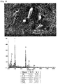
- the copper alloy of the present invention improves electric conductivity and strength by forming Cr-Si group deposits by coupling of the Cr and Si in a Cu matrix, wherein, if a content of the Cr is below 0.01wt%, it is difficult to secure the strength and improve workability due to shortage of formation of the deposits, and if the content of the Cr exceeds 0.25wt%, poor conductivity is resulted in due to coarse Cr-Si group deposits.
- FIG. 3 illustrates a photograph of a scanning electron microscope showing Cr-Si group deposits in a copper matrix.
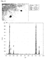
- the copper alloy of the present invention improves electric conductivity and strength by forming Mg-P group deposits by coupling of the Mg and P in a Cu matrix, wherein, if a content of the Mg is below 0.01wt%, it is difficult to secure the strength due to shortage of formation of the deposits, and if the content of the Mg exceeds 0.25wt%, significant drop of the electric conductivity or poor bending workability is resulted in and production cost increases.
- FIG. 4 illustrates a photograph of a scanning electron microscope showing Mg-P group deposit in a copper matrix.
- the copper alloy of the present invention fails to contribute to the strength due to inadequate formation of the deposits in steps after the steps of melting, casting, and heating ingot, and if the content of the Si exceeds 0.15wt%, the copper alloy of the present invention shows improvement on above effect no more, as well as significant drop of the conductivity.
- FIG. 2 illustrates a photograph of a scanning electron microscope showing Mg-Si group deposit in a copper matrix.
- P is a major element has an oxidizing action, forms deposits with Fe and Mg, and improves strength or heat resistance of the copper alloy, wherein, if the content of the P is below 0.025wt%, no adequate strength or heat resistance are obtained due to inadequate formation of the deposits, and if the content of the P exceeds 0.15wt%, not only the conductivity, but also the heat resistance, hot workability, and press workability become poor.
- the composition may include less than 1.0wt% of at least one kind of Zn, Sn, Mn, Al, and Ni, wherein the element affects the electric conductivity and the strength, and if added over 1.0wt%, though the strength increases, the electric conductivity drops.
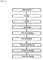
- the present invention provides a method for preparing a high strength and high conductivity copper alloy, including the steps of obtaining molten metal of the composition, casting the molten metal to obtain an ingot, and subjecting the ingot to hot rolling at 850 ⁇ 1,000°C, cold rolling after cooling, annealing (First annealing) at 400 - 600°C for 1 ⁇ 10 hours, intermediate rolling (Second cold rolling) with a reduction ratio of 30 ⁇ 70%, heat treating (Second annealing) at 500 ⁇ 800°C for 30 ⁇ 600 seconds, and finish rolling (Final cold rolling) down to 20 - 40%.
- a proper condition at the first annealing is 400 - 600°C for 1 ⁇ 10 hours, wherein, if the 600°C is exceeded, and the 10 hours is exceeded, the temperature and annealing time period affects the strength directly, and the high temperature and long annealing time period shows reduction of the electric conductivity on the contrary, and if the temperature is below the 400°C, and the annealing time period is below one hour, securing the deposits or recrystallization is inadequate.
- the second annealing is a distortion removal annealing, wherein, if the annealing is performed at a temperature below 500°C and in a time period below 30 seconds, distortion caused by pressing can not be removed adequately, and if the annealing is performed at a temperature over 750°C and in a time period over 600 seconds, softening of the material progresses, failing to obtain a desired material properties.
- An alloy on table 1 is melted in a high frequency melting furnace to form an ingot, with a thickness of 22mm, a width of 40mm, and a length of 180mm.
- the ingot is subjected to heating at a temperature of 950°C for one hour, hot rolling down to a thickness of 10mm, 1 mm surface machining at each side, and cold rolling down to 1.5mm.
- the cold rolled material is subjected to heat treatment at a temperature of 480°C for three hours, cold rolling down to 0.4mm, distortion removal annealing at a temperature of 650°C, and finish rolling down to 0.25mm, to obtain a cold rolled material shown on table 2.
- the cold rolled material is subjected to selective seasoning, acid cleaning and polishing, a second heat treatment, and correction processing with a tension leveler.
- the method in accordance with the preferred embodiment of the present invention is not limited to this, but may combine steps according to requirements from clients selected from the steps of hot rolling, cold rolling, seasoning, surface cleaning (acid cleaning and polishing), tension annealing, tension leveling, and so on the same as normal practice made in a copper stretching shop for meeting different quality requirements from clients.
- test pieces obtained from the composition and through the preparation process is cut and subjected to tensile strength (TS) test and electric conductivity (EC) test to obtain a test result as shown in table 2.
- TS tensile strength
- EC electric conductivity
- Tensile strength is measured in accordance with KS B0802, and electric conductivity is measured in accordance with KS D0240.
- the specimens 1 to 10 of the present invention are excellent alloys showing good harmony of strength and electric conductivity in comparison to comparative examples 1 ⁇ 13 and the related art C19210 and CDA194.
- each of specimens 1 to 10 according to the present invention has electric conductivity more or less poorer than the related art C19210 (85%IACS), since each of the specimens 1 to 10 of the present invention has tensile strength of over 52N/mm 2 which is very excellent in comparison to 38N/mm 2 of the C19210, the specimens 1 to 10 of the present invention are evaluated as alloys showing good harmony of the strength and the electric conductivity.
- specimens 1 to 10 of the present invention are alloys each with excellent strength and electric conductivity with good harmony of the strength and the electric conductivity compared to CDA194.
- the present invention can be utilized widely as a copper alloy material for semiconductor lead frame material, LED lead frame material, connector terminal and so on having high conductibility and high workability while increasing or maintaining tensile strength.
Landscapes
- Chemical & Material Sciences (AREA)
- Engineering & Computer Science (AREA)
- Materials Engineering (AREA)
- Mechanical Engineering (AREA)
- Metallurgy (AREA)
- Organic Chemistry (AREA)
- Physics & Mathematics (AREA)
- Thermal Sciences (AREA)
- Crystallography & Structural Chemistry (AREA)
- Condensed Matter Physics & Semiconductors (AREA)
- General Physics & Mathematics (AREA)
- Computer Hardware Design (AREA)
- Microelectronics & Electronic Packaging (AREA)
- Power Engineering (AREA)
- Conductive Materials (AREA)
Applications Claiming Priority (2)
| Application Number | Priority Date | Filing Date | Title |
|---|---|---|---|
| KR1020100011356A KR101260911B1 (ko) | 2010-02-08 | 2010-02-08 | 고강도, 고전도성을 갖는 동합금 및 그 제조방법 |
| PCT/KR2010/007462 WO2011096632A2 (ko) | 2010-02-08 | 2010-10-28 | 고강도, 고전도성을 갖는 동합금 및 그 제조방법 |
Publications (1)
| Publication Number | Publication Date |
|---|---|
| EP2535433A2 true EP2535433A2 (en) | 2012-12-19 |
Family
ID=44355896
Family Applications (1)
| Application Number | Title | Priority Date | Filing Date |
|---|---|---|---|
| EP10845319A Withdrawn EP2535433A2 (en) | 2010-02-08 | 2010-10-28 | Copper alloy having high strength and high conductivity, and preparation method thereof |
Country Status (6)
| Country | Link |
|---|---|
| US (1) | US20120312430A1 (ko) |
| EP (1) | EP2535433A2 (ko) |
| JP (1) | JP5461711B2 (ko) |
| KR (1) | KR101260911B1 (ko) |
| CN (1) | CN102782168A (ko) |
| WO (1) | WO2011096632A2 (ko) |
Families Citing this family (11)
| Publication number | Priority date | Publication date | Assignee | Title |
|---|---|---|---|---|
| KR20130136183A (ko) * | 2012-06-04 | 2013-12-12 | 박효주 | 동합금부재와 그 제조 방법 |
| KR101463092B1 (ko) * | 2012-08-21 | 2014-11-21 | 한국철도기술연구원 | 고강도 및 고전도 고속전철용 전차선 |
| JP5851000B1 (ja) * | 2014-08-22 | 2016-02-03 | 株式会社神戸製鋼所 | Ledのリードフレーム用銅合金板条 |
| CN104928527A (zh) * | 2015-07-13 | 2015-09-23 | 苏州科茂电子材料科技有限公司 | 一种电缆用导电铜材料及其制备方法 |
| KR101834335B1 (ko) * | 2017-11-02 | 2018-04-13 | 주식회사 풍산 | 고강도 및 고전기전도도 특성을 가진 전기전자 부품 및 반도체용 동합금 및 이의 제조 방법 |
| CN108754218B (zh) * | 2018-09-10 | 2019-09-10 | 江西理工大学 | 一种高强高导Cu-Cr-Fe-Mg-P合金线材及其制备方法 |
| KR101965345B1 (ko) * | 2018-12-19 | 2019-04-03 | 주식회사 풍산 | 굽힘가공성이 우수한 단자 및 커넥터용 구리합금 및 이의 제조방법 |
| KR102120295B1 (ko) * | 2018-12-26 | 2020-06-08 | 태원공업(주) | 양백각선의 제조 방법 |
| CN111020283B (zh) * | 2019-12-06 | 2021-07-20 | 宁波金田铜业(集团)股份有限公司 | 插件用铜合金带材及其制备方法 |
| CN114657410B (zh) * | 2022-04-06 | 2022-09-09 | 中南大学 | 一种高强高导铜铁系合金及其制备方法 |
| CN114774733B (zh) * | 2022-04-28 | 2023-05-26 | 郑州大学 | 一种铸轧辊套用高性能铜基合金材料及其制备方法 |
Family Cites Families (10)
| Publication number | Priority date | Publication date | Assignee | Title |
|---|---|---|---|---|
| JPH0676630B2 (ja) | 1986-12-23 | 1994-09-28 | 三井金属鉱業株式会社 | 配線接続具用銅合金 |
| JP4042920B2 (ja) * | 1995-02-21 | 2008-02-06 | 三菱伸銅株式会社 | 強度および打抜き加工性に優れた電気電子部品用Cu合金 |
| JP3717321B2 (ja) | 1998-12-11 | 2005-11-16 | 古河電気工業株式会社 | 半導体リードフレーム用銅合金 |
| JP3318309B2 (ja) | 2000-02-29 | 2002-08-26 | 日鉱金属株式会社 | リードフレームおよびリードフレーム用銅合金 |
| KR100366843B1 (ko) * | 2000-10-09 | 2003-01-09 | 한국카파매트리얼 주식회사 | 동합금 및 그의 제조방법 |
| JP3856018B2 (ja) * | 2004-06-03 | 2006-12-13 | 日立電線株式会社 | 高強度・高導電性銅合金の製造方法 |
| CN100439530C (zh) * | 2004-12-24 | 2008-12-03 | 株式会社神户制钢所 | 具有弯曲性和应力弛豫性能的铜合金 |
| JP3838521B1 (ja) * | 2005-12-27 | 2006-10-25 | 株式会社神戸製鋼所 | 高強度および優れた曲げ加工性を備えた銅合金およびその製造方法 |
| JP2008024995A (ja) * | 2006-07-21 | 2008-02-07 | Kobe Steel Ltd | 耐熱性に優れた電気電子部品用銅合金板 |
| JP5214282B2 (ja) * | 2008-03-07 | 2013-06-19 | 株式会社神戸製鋼所 | ダイシング加工性に優れるqfnパッケージ用銅合金板 |
-
2010
- 2010-02-08 KR KR1020100011356A patent/KR101260911B1/ko active IP Right Grant
- 2010-10-28 US US13/577,512 patent/US20120312430A1/en not_active Abandoned
- 2010-10-28 JP JP2012552786A patent/JP5461711B2/ja active Active
- 2010-10-28 EP EP10845319A patent/EP2535433A2/en not_active Withdrawn
- 2010-10-28 WO PCT/KR2010/007462 patent/WO2011096632A2/ko active Application Filing
- 2010-10-28 CN CN2010800633983A patent/CN102782168A/zh active Pending
Non-Patent Citations (1)
| Title |
|---|
| See references of WO2011096632A2 * |
Also Published As
| Publication number | Publication date |
|---|---|
| JP5461711B2 (ja) | 2014-04-02 |
| KR20110091973A (ko) | 2011-08-17 |
| WO2011096632A3 (ko) | 2011-10-20 |
| US20120312430A1 (en) | 2012-12-13 |
| CN102782168A (zh) | 2012-11-14 |
| JP2013518993A (ja) | 2013-05-23 |
| KR101260911B1 (ko) | 2013-05-06 |
| WO2011096632A2 (ko) | 2011-08-11 |
Similar Documents
| Publication | Publication Date | Title |
|---|---|---|
| EP2535433A2 (en) | Copper alloy having high strength and high conductivity, and preparation method thereof | |
| JP4943095B2 (ja) | 銅合金及びその製造方法 | |
| KR102126731B1 (ko) | 구리합금 판재 및 구리합금 판재의 제조 방법 | |
| JP4787986B2 (ja) | 銅合金およびその製造方法 | |
| WO2006019035A1 (ja) | 曲げ加工性を備えた電気電子部品用銅合金板 | |
| KR20170113410A (ko) | 구리합금 판재 및 구리합금 판재의 제조 방법 | |
| CN108699641B (zh) | Al-Mg-Si系合金材料、Al-Mg-Si系合金板和Al-Mg-Si系合金板的制造方法 | |
| US8652274B2 (en) | Copper alloy with high strength and high conductibility, and method for manufacturing same | |
| JP2017179445A (ja) | Al−Mg―Si系合金板 | |
| KR102210703B1 (ko) | 강도 및 굽힘가공성이 우수한 자동차 또는 전기전자 부품용 동합금판재의 제조 방법 및 이로부터 제조된 동합금판재 | |
| CN110872665B (zh) | Al-Mg-Si系合金板 | |
| JP6533401B2 (ja) | Cu−Ni−Si系銅合金板材およびその製造方法並びにリードフレーム | |
| JP4664584B2 (ja) | 高強度銅合金板および高強度銅合金板の製造方法 | |
| KR102403910B1 (ko) | 강도, 전기전도도 및 굽힘가공성이 우수한 자동차 또는 전기전자 부품용 동합금판재의 제조 방법 및 이로부터 제조된 동합금판재 | |
| JP6793005B2 (ja) | 銅合金板材およびその製造方法 | |
| JP5748945B2 (ja) | 銅合金材の製造方法とそれにより得られる銅合金材 | |
| KR101031816B1 (ko) | 리드프레임용 동합금의 제조방법 | |
| JPH07242965A (ja) | メッキ性および導電性に優れた銅合金およびこの銅合金からなる薄板または条 | |
| KR20230030578A (ko) | 구리 합금, 구리 합금 소성 가공재, 전자·전기 기기용 부품, 단자, 버스 바, 리드 프레임, 방열 기판 | |
| WO2017168891A1 (ja) | Al-Mg―Si系合金板の製造方法 | |
| JP4449254B2 (ja) | 熱間加工性および切削性に優れた銅合金 | |
| KR101060529B1 (ko) | 고강도 및 고전도성 동합금 및 그 제조방법 | |
| JP2001158927A (ja) | 熱間加工性に優れた銅合金 | |
| KR20100092096A (ko) | 고강도 및 도전성 동합금 및 그 제조방법 | |
| TW202212583A (zh) | 銅合金、銅合金塑性加工材、電子電氣機器用零件、端子、散熱基板 |
Legal Events
| Date | Code | Title | Description |
|---|---|---|---|
| PUAI | Public reference made under article 153(3) epc to a published international application that has entered the european phase |
Free format text: ORIGINAL CODE: 0009012 |
|
| 17P | Request for examination filed |
Effective date: 20120813 |
|
| AK | Designated contracting states |
Kind code of ref document: A2 Designated state(s): AL AT BE BG CH CY CZ DE DK EE ES FI FR GB GR HR HU IE IS IT LI LT LU LV MC MK MT NL NO PL PT RO RS SE SI SK SM TR |
|
| DAX | Request for extension of the european patent (deleted) | ||
| STAA | Information on the status of an ep patent application or granted ep patent |
Free format text: STATUS: THE APPLICATION IS DEEMED TO BE WITHDRAWN |
|
| 18D | Application deemed to be withdrawn |
Effective date: 20160503 |