EP2530700B1 - Verfahren zur Herstellung dünner Proben zur TEM-Abbildung - Google Patents
Verfahren zur Herstellung dünner Proben zur TEM-Abbildung Download PDFInfo
- Publication number
- EP2530700B1 EP2530700B1 EP12170383.9A EP12170383A EP2530700B1 EP 2530700 B1 EP2530700 B1 EP 2530700B1 EP 12170383 A EP12170383 A EP 12170383A EP 2530700 B1 EP2530700 B1 EP 2530700B1
- Authority
- EP
- European Patent Office
- Prior art keywords
- sample
- thinning
- ion beam
- depositing
- face
- Prior art date
- Legal status (The legal status is an assumption and is not a legal conclusion. Google has not performed a legal analysis and makes no representation as to the accuracy of the status listed.)
- Active
Links
Images


Classifications
-
- G—PHYSICS
- G01—MEASURING; TESTING
- G01N—INVESTIGATING OR ANALYSING MATERIALS BY DETERMINING THEIR CHEMICAL OR PHYSICAL PROPERTIES
- G01N1/00—Sampling; Preparing specimens for investigation
- G01N1/28—Preparing specimens for investigation including physical details of (bio-)chemical methods covered elsewhere, e.g. G01N33/50, C12Q
- G01N1/32—Polishing; Etching
-
- G—PHYSICS
- G01—MEASURING; TESTING
- G01N—INVESTIGATING OR ANALYSING MATERIALS BY DETERMINING THEIR CHEMICAL OR PHYSICAL PROPERTIES
- G01N1/00—Sampling; Preparing specimens for investigation
- G01N1/28—Preparing specimens for investigation including physical details of (bio-)chemical methods covered elsewhere, e.g. G01N33/50, C12Q
- G01N1/286—Preparing specimens for investigation including physical details of (bio-)chemical methods covered elsewhere, e.g. G01N33/50, C12Q involving mechanical work, e.g. chopping, disintegrating, compacting, homogenising
-
- H—ELECTRICITY
- H01—ELECTRIC ELEMENTS
- H01J—ELECTRIC DISCHARGE TUBES OR DISCHARGE LAMPS
- H01J37/00—Discharge tubes with provision for introducing objects or material to be exposed to the discharge, e.g. for the purpose of examination or processing thereof
- H01J37/02—Details
-
- H—ELECTRICITY
- H01—ELECTRIC ELEMENTS
- H01J—ELECTRIC DISCHARGE TUBES OR DISCHARGE LAMPS
- H01J37/00—Discharge tubes with provision for introducing objects or material to be exposed to the discharge, e.g. for the purpose of examination or processing thereof
- H01J37/30—Electron-beam or ion-beam tubes for localised treatment of objects
- H01J37/305—Electron-beam or ion-beam tubes for localised treatment of objects for casting, melting, evaporating or etching
- H01J37/3053—Electron-beam or ion-beam tubes for localised treatment of objects for casting, melting, evaporating or etching for evaporating or etching
- H01J37/3056—Electron-beam or ion-beam tubes for localised treatment of objects for casting, melting, evaporating or etching for evaporating or etching for microworking, e.g. etching of gratings, trimming of electrical components
-
- H—ELECTRICITY
- H01—ELECTRIC ELEMENTS
- H01L—SEMICONDUCTOR DEVICES NOT COVERED BY CLASS H10
- H01L21/00—Processes or apparatus adapted for the manufacture or treatment of semiconductor or solid state devices or of parts thereof
- H01L21/02—Manufacture or treatment of semiconductor devices or of parts thereof
- H01L21/02104—Forming layers
- H01L21/02107—Forming insulating materials on a substrate
- H01L21/02296—Forming insulating materials on a substrate characterised by the treatment performed before or after the formation of the layer
- H01L21/02318—Forming insulating materials on a substrate characterised by the treatment performed before or after the formation of the layer post-treatment
-
- G—PHYSICS
- G01—MEASURING; TESTING
- G01N—INVESTIGATING OR ANALYSING MATERIALS BY DETERMINING THEIR CHEMICAL OR PHYSICAL PROPERTIES
- G01N1/00—Sampling; Preparing specimens for investigation
- G01N1/28—Preparing specimens for investigation including physical details of (bio-)chemical methods covered elsewhere, e.g. G01N33/50, C12Q
- G01N1/286—Preparing specimens for investigation including physical details of (bio-)chemical methods covered elsewhere, e.g. G01N33/50, C12Q involving mechanical work, e.g. chopping, disintegrating, compacting, homogenising
- G01N2001/2873—Cutting or cleaving
- G01N2001/2886—Laser cutting, e.g. tissue catapult
-
- H—ELECTRICITY
- H01—ELECTRIC ELEMENTS
- H01J—ELECTRIC DISCHARGE TUBES OR DISCHARGE LAMPS
- H01J2237/00—Discharge tubes exposing object to beam, e.g. for analysis treatment, etching, imaging
- H01J2237/20—Positioning, supporting, modifying or maintaining the physical state of objects being observed or treated
-
- H—ELECTRICITY
- H01—ELECTRIC ELEMENTS
- H01J—ELECTRIC DISCHARGE TUBES OR DISCHARGE LAMPS
- H01J2237/00—Discharge tubes exposing object to beam, e.g. for analysis treatment, etching, imaging
- H01J2237/26—Electron or ion microscopes
- H01J2237/28—Scanning microscopes
- H01J2237/2802—Transmission microscopes
-
- H—ELECTRICITY
- H01—ELECTRIC ELEMENTS
- H01J—ELECTRIC DISCHARGE TUBES OR DISCHARGE LAMPS
- H01J2237/00—Discharge tubes exposing object to beam, e.g. for analysis treatment, etching, imaging
- H01J2237/30—Electron or ion beam tubes for processing objects
- H01J2237/317—Processing objects on a microscale
- H01J2237/3174—Etching microareas
- H01J2237/31745—Etching microareas for preparing specimen to be viewed in microscopes or analyzed in microanalysers
Definitions
- the present invention relates to preparation of thin samples for transmission electron microscopy and, in particular, to preparation of high quality samples less than 60 nm in thickness.
- a semiconductor substrate on which circuits are being formed usually a silicon wafer, is coated with a material, such as a photoresist, that changes solubility when exposed to radiation.
- a lithography tool such as a mask or reticle, positioned between the radiation source and the semiconductor substrate casts a shadow to control which areas of the substrate are exposed to the radiation. After the exposure, the photoresist is removed from either the exposed or the unexposed areas, leaving a patterned layer of photoresist on the wafer that protects parts of the wafer during a subsequent etching or diffusion process.
- the photolithography process allows multiple integrated circuit devices or electromechanical devices, often referred to as "chips," to be formed on each wafer.
- the wafer is then cut up into individual dies, each including a single integrated circuit device or electromechanical device.
- these dies are subjected to additional operations and packaged into individual integrated circuit chips or electromechanical devices.
- CD measurements are made using instruments such as a scanning electron microscope (SEM).
- SEM scanning electron microscope
- a primary electron beam is focused to a fine spot that scans the surface to be observed.
- Secondary electrons are emitted from the surface as it is impacted by the primary beam.
- the secondary electrons are detected, and an image is formed, with the brightness at each point of the image being determined by the number of secondary electrons detected when the beam impacts a corresponding spot on the surface.
- TEMs Transmission electron microscopes
- SEMs which only image the surface of a material
- TEM also allows analysis of the internal structure of a sample.
- a broad beam impacts the sample and electrons that are transmitted through the sample are focused to form an image of the sample.
- the sample must be sufficiently thin to allow many of the electrons in the primary beam to travel though the sample and exit on the opposite site. Samples are typically less than 100 nm thick.
- a primary electron beam is focused to a fine spot, and the spot is scanned across the sample surface. Electrons that are transmitted through the substrate are collected by an electron detector on the far side of the sample, and the intensity of each point on the image corresponds to the number of electrons collected as the primary beam impacts a corresponding point on the surface.
- STEM scanning transmission electron microscope
- TEM transmission electron microscopes
- the term "TEM” as used herein refers to a TEM or a STEM, and references to preparing a sample for a TEM are to be understood to also include preparing a sample for viewing on an STEM.
- a broad beam impacts the sample and electrons that are transmitted through the sample are focused to form an image of the sample.
- the sample must be sufficiently thin to allow many of the electrons in the primary beam to travel though the sample and exit on the opposite site.
- Lamellae Thin TEM samples cut from a bulk sample material are known as "lamellae.” Lamellae are typically less than 100 nm thick, but for some applications a lamella must be considerably thinner. With advanced semiconductor fabrication processes at 30 nm and below, a lamella needs to be less than 20 nm in thickness in order to avoid overlap among small-scale structures. Currently thinning below 60 nm is difficult and not robust. Thickness variations in the sample result in lamella bending, over-milling, or other catastrophic defects. For such thin samples, lamella preparation is a critical step in TEM analysis that significantly determines the quality of structural characterization and analysis of the smallest and most critical structures.
- FIB focused ion beam
- FIB systems are capable of milling lamellae sufficiently thin to be used in a TEM system.
- dual-beam systems for TEM sample preparation is known in the art.
- a dual-beam system has a FIB column for milling a lamella from a bulk sample and a SEM column for imaging the lamella, typically as the lamella is being milled. Dual-beam systems improve the time required to prepare samples for TEM analysis.
- FIG. 1 shows a prior art FIB system in an initial orientation for preparing a sample lamella for TEM analysis from a bulk sample material.
- Bulk sample material 108 is loaded into sample stage and oriented so that its top surface is perpendicular to focused ion beam 104 emitted from a FIB column.
- a focused ion beam using a high beam current with a correspondingly large beam size is used to mill large amounts of material away from the front and back portion of the region of interest.
- the remaining material between the two milled rectangles 14 and 15 forms a thin vertical sample section 102 that includes an area of interest.
- the sample section is thinned (typically using progressively finer beam sizes and lower beam energy) until the desired thickness (typically less than 100 nm) is reached.
- Most of the ion beam machining done to create lamella 110 is performed with bulk sample material 108 and FIB column in this orientation.
- the stage is typically tilted and a U-shaped cut is made at an angle partially along the bottom and sides of the sample section 102, leaving the sample hanging by tabs at either side at the top of the sample.
- the small tabs allow the least amount of material to be milled free after the sample is completely FIB polished, reducing the possibility of redeposition artifacts accumulating on the thin specimen.
- the sample section is then further thinned using progressively finer beam sizes. Finally, the tabs are cut to completely free the thinned lamella 110. After thinning the sample is freed from the bulk material at the sides and bottom, and the thinned TEM sample can be extracted.
- ultra thin lamellae formed using the prior art methods described above are subject to undesirable side effects known as “bending” and “curtaining.”
- the sample When attempting to produce ultra thin samples (for example, 30 nm thickness or less) the sample may lose structural integrity and deform under forces acting on the sample, typically by bending or bowing toward one sample face or the other. If this occurs during or prior to a FIB thinning step, then the deformation of the region of interest toward or away from the beam may cause unacceptable damage to the sample.
- Thickness variations caused by a milling artifact known as "curtaining” can also have a significant effect on TEM sample quality.
- ion beam 104 preferentially mills the lighter elements at a higher mill rate.
- the heavier metal elements tend to shadow the lighter material underneath them.
- the resulting effect is a rippled lamella face which is not milled back as far in the areas of metal as it is milled in the areas without metal.
- FIG. 2 is a photomicrograph of a thinned TEM sample 102 showing curtaining on one sample face, in which the rippled features on the lamella face resemble a hanging curtain.
- curtaining artifacts reduce the quality of the TEM imaging and limit the minimal useful specimen thickness.
- the two cross-section faces are in very close proximity so thickness variations from curtaining effects can cause a sample lamella to be unusable.
- backside milling works reasonably well for TEM samples having a thickness of 50 to 100 nm, but for ultra-thin samples having a sample thickness of 30 nm or less, even samples prepared by backside milling often show milling artifacts resulting in an undesirably non-uniform sample face. Further, even for thicker samples, backside milling requires a liftout and inversion operation that is very time consuming. Current backside milling techniques are also performed manually, and are unsuitable for automation.
- JP H11 58033 A (NIPPON TELEGRAPH & TELEPHONE) 2 March 1999 (1999-03-02) discloses to lessen the influence of the surface roughening by microcrystal formation of indium by depositing an element to lower the m.p. by eutectic reaction with the indium or an element to suppress the diffusion of the indium by evaporation on a sample surface simultaneously with ion beam irradiation, thereby eliminating the need for cooling equipment and the device to be exclusively used for generating a halogen element beam.
- An object of the invention is to provide a method and apparatus for preparing TEM samples less than 60 nanometers thick, more preferably 30 nm or less in thickness, in a manner that reduces or prevents bending and curtaining. This is achieved by the method of claim 1, the apparatus of claim 11 and the storage medium of claim 12.
- the invention addresses problems of bending and curtaining during TEM sample preparation by adding material to the sample during the process of preparing the sample.
- the present invention actually deposits additional material back onto the sample during sample preparation.
- a material can be deposited onto a first TEM sample face after the first face has been thinned, but before the second face is thinned.
- all of the deposited material can be left on the thinned first sample face while the second sample face is thinned.
- most of the deposited material can be removed from the first thinned side before the second side is thinned.
- the deposited material left behind can serve to fill in the areas over-thinned by curtaining effects. In either case, the presence of deposited material on the sample face opposite the face being FIB milled can serve to reinforce the structural integrity of the sample.
- material is deposited onto the sample face as it being thinned.
- undesirable curtaining effects often result when a sample is composed of a mixture of more rapidly milling and slower milling materials.
- Applicants have discovered that by conducting the milling process in the presence of a suitable precursor gas, material can be simultaneously deposited on some parts of the sample surface while other parts of the surface are being milled away.
- the sample face can be coated after a fraction of the FIB thinning has been performed on the face. By either or both of these methods, the areas of the sample face having a higher milling rate can be protected or even re-filled by deposited material during the thinning process, thus reducing or preventing curtaining of the sample face.
- some or all of the deposited material is removed before sample imaging; in other examples the material deposited is sufficiently electron transparent at the desired imaging parameters that it can be left in place during sample TEM analysis.
- any known suitable method can be used for material removal.
- a suitable material removal method will depend upon a number of factors such as the material deposited and the structural integrity of the sample.
- the selected material removal method will selectively remove the deposited material causing little if any additional sample material removal from the TEM sample.
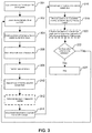
- FIG. 3 is a flowchart showing the steps of creating a TEM sample according to an example useful for understanding the present invention.
- a substrate such as a semiconductor wafer, a frozen biological material, or a mineral sample is loaded into a suitable processing tool such as a Dual Beam FIB/SEM system having both a FIB column and a SEM column.
- a suitable processing tool such as a Dual Beam FIB/SEM system having both a FIB column and a SEM column.
- a suitable beam FIB/SEM system is the Helios1200 or the ExpidaTM 1255 DualBeamTM System, available from FEI Company of Hillsboro, OR, the assignee of the present invention.
- the typical dual-beam system 702 configuration is an electron column 704 having a vertical axis with an ion column 706 having an axis tilted with respect to the vertical (usually at a tilt of approximately 52 degrees).
- Wafers are preferably transferred by way of a multi-wafer carrier and auto-loading robot (not shown), as is well known in the art, although wafers can also be transferred manually.
- the location of a TEM sample (containing a feature of interest) to be extracted from a substrate is determined.
- the substrate may be a silicon semiconductor wafer or portion thereof and the portion to be extracted may include a portion of an integrated circuit formed on the silicon wafer that is to be observed using the TEM.
- the substrate could be an AlTiC wafer and the extracted portion might include a structure used for reading or writing data onto a storage medium.
- the substrate could be a sample containing a natural resource and extraction might be performed to analyze characteristics of the resource in the sample.
- FIG. 4 is a schematic representation showing the location of the sample 102 to be extracted within a larger substrate 108.
- the substrate is preferably oriented so that its top surface is perpendicular to a focused ion beam emitted from the FIB column 706.
- a focused ion beam using a high beam current with a correspondingly large beam size is then used to mill large amounts of material away from the front and back portion of a sample section containing the desired TEM sample in step 306.
- Bulk material removal is preferably performed at high beam current, preferably at highest controllable current available in order remove the bulk material as fast as possible. For example, bulk material removal could be performed using a 13 nA gallium ion beam with a 30 kV accelerating voltage. In some circumstances it may be desirable to mill the substrate with the TEM sample oriented at an acute angle relative to the substrate surface.
- U.S. Pat. No. 6,039,000 to Libby et al for Focused Particle Beam Systems and Methods Using a Tilt Column (2000), which is assigned to the assignee of the present invention, describes creating a TEM sample using a FIB oriented at an angle relative to the sample surface by etching a cavity on either side of desired TEM sample.
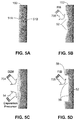
- FIG. 5A shows such a vertical sample section 102, although none of the surrounding bulk substrate is shown for clarity.
- the sample section 102 is then further thinned on a first side 51A (preferably using progressively finer beam sizes and lower beam energy) until the desired first sample face is reached.
- the first phase of thinning might use a beam current of 1 nA ion beam, followed by a second phase using a 100 pA beam.
- the exposed first sample face will typically display some degree of curtaining, resulting in over-milled areas 52.
- the sample is preferably thinned using an ion beam with an axis oriented normal or perpendicular to the top surface of the sample, although a non-normal angle could also be used if the beam axis is oriented to the side of the desired TEM sample face.
- FIG. 5B The differences in material thickness shown in FIG. 5B is only for illustration purposes and not intended to show exact scale of difference in thickness between the working surface and the troughs caused by curtaining or to indicate that the surface variations will necessarily be uniform.
- the arrows indicating the FIB 706 and SEM beam 704 or other processes shown schematically in FIGS. 5B-5I are only intended to illustrate the process being applied, not the angle or orientation of the beams or the exact location of the deposition or etching.
- step 310 once the desired sample face has been exposed, material 56 is deposited onto the exposed sample face.
- a layer of material 56 is deposited onto the entire sample face, for example, by using a precursor gas 54 and chemical vapor deposition, using either the ion beam or an electron beam (depending in part upon the material being deposited).
- the mechanism for activating the precursors could be SEM, FIB, indirect delivery of secondary particles, or other techniques. Further, the deposition technique is not limited to beam activated precursor deposition.
- the material deposited preferably has a different composition than the TEM sample material(s).
- the choice of material to be deposited may depend upon the particular application of the TEM sample. Suitable deposited materials may include, for example, tungsten, platinum, gold, carbon, silicon oxides, or any other suitable materials. Precursor gases for depositing these materials are well known in the prior art.
- the deposited material either will be removed during the thinning process or will be easily removable after the critical milling of the TEM sample is completed.
- the deposition material is carbon, which can be deposited by carbon vapor deposition
- the deposition material can be removed through water vapor etching, which is a very selective etching process that will not cause additional damage to the non-carbon TEM sample.
- the deposited material may be one which will not significantly interfere with imaging the TEM sample, in which case it can be left in place. For instance, in applications involving chemical analysis of the sample, the known compounds present in deposited material can be ignored.
- material 56 is added so that the overall thickness of the original sample section 102 is increased. In other words, more material is added than was removed during the thinning process. This amount of additional material is not required, however, as long as the added material is sufficient to adequately increase the structural integrity of the sample or to fill in a sufficient amount of the curtaining over-milling.
- the thickness of the deposited layer of thickness depends on how much beam exposure is expected and what material is being deposited. For example, if a Carbon-based material is deposited mainly for the purpose of structural integrity and it will receive minimal erosion from beam exposure, then a deposition layer of approximately 20 nm might be appropriate. If the layer is being used to reduce curtaining during a 1 nA milling step, then a thickness of 100 nm or more might be deposited.
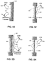
- a portion of the added material 56 is optionally removed. Because the deposited material is composed of a single compound, little or no curtaining will result as the material is removed. Preferably enough deposited material 56 is left on the sample face 51A to provide additional structural integrity as the other sample face 51 B is milled, although all of the deposited material could be removed before proceeding to the second sample face in situations where sample bending is a low priority and the only real concern is the reduction in curtaining. As discussed below, material can be deposited onto the sample before the final sample face is exposed. The deposited material could then be removed during subsequent additional thinning. The steps of thinning, adding material, and thinning again could be repeated iteratively until the final sample face is exposed. This iterative technique can be useful in minimizing the curtaining effect or if it is desirable can be employed as an end-pointing technique of the thinning step.
- the FIB is directed at the second TEM sample face 51 B (backside) of sample 102 to thin the sample.
- the first phase of thinning might use a beam current of 1 nA ion beam, followed by a second phase using a 100 pA beam.
- the exposed second sample face 51 B will typically also display some degree of curtaining, resulting in over-milled areas 52.
- step 316 material 56 is also deposited onto the second sample face 51 B using a suitable process such as chemical vapor deposition.
- step 318 some or all of the deposited material on the second face is removed, for example by FIB milling. The material deposited on the backside would also be added and removed iteratively in multiple steps, with all of the material removed on the final thinning step.
- step 320 all of the deposited material 56 can be removed from the completed TEM sample 110.
- the material removal can be accomplished via FIB milling, or by a method that will be less destructive to the TEM sample material such as a selective gas-assisted etching, either with the ion beam or with an electron beam.
- the deposited material can be etched away in, for example, an acid bath after the TEM sample is removed from the vacuum chamber. The present disclosure is not limited to these examples, and any suitable type of beam-based removal or chemistry removal, or plasma induced removal may be utilized. If there are other samples to be extracted from the substrate (step 322) the process returns to step 302 and the next sample site is located. If not, in step 324 the process stops.
- material is deposited onto the TEM sample face during the thinning process.
- two charged particle beams could be used at one time.
- the electron beam could be used with a suitable precursor gas to deposit the material onto the sample face, while the FIB could be used for milling.
- an ion beam is used to deposit and remove material at the same time.
- a focused ion beam system typically has a circularly symmetric, substantially Gaussian current density distribution, as illustrated in FIG. 6 , which shows a graph of ion current density versus position along a radial axis. As shown in FIG. 6 , the current density at the center of the beam is highest (and thus mills faster) while the beam current tapers off away from the center of the beam.
- This beam current spread is one of the main contributors to curtaining. As the beam is milling the lamella face with the center of the beam, the ions in the tail of the Gaussian distribution are reaching sample material in advance of (and behind) the center of the beam. The lower current portion of the beam may have little effect upon the heavier metal sample structures having low milling rates; however, the lighter materials with higher milling rates may be milled to a significant degree.
- this "advance" milling can be reduced or eliminated by directing a suitable precursor gas toward the sample surface in the presence of the beam.
- a suitable precursor gas As is well known in the prior art, when the charged particle beam irradiates the substrate with the adsorbed layer of precursor gas, secondary electrons are emitted from the substrate. These secondary electrons cause a dissociation of the adsorbed precursor gas molecules. Part of the dissociated precursor material forms a deposit on the substrate surface, while the rest of the precursor gas particle forms a volatile by-product and is pumped away by the vacuum system of the apparatus.
- the outlying lower current portions of the beam can provide secondary electrons to cause deposition of the dissociated precursor material.
- This deposited material must then be sputtered away before the underlying substrate is milled.
- the beam current in the center of the beam is high enough to switch the dominant reaction from deposition to milling.
- the deposited material can serve as a protective layer to prevent significant milling of the lighter, higher milling rate material in advance of the center of the beam, while the center of the beam mills away both the newly deposited protective layer and the underlying substrate at roughly the same rate.
- the lighter material covered by a protective layer will not etch significantly and curtaining will be prevented or at least substantially reduced.
- Skilled persons will be able to select a suitable precursor gas and adjust the gas pressure and beam current so that the predominant reaction is deposition at the outlying lower current portions of the beam and etching (milling) at the center of the beam.
- the rate of deposition may be higher than the rate of etching even for the center of the beam so that a protective layer is deposited on the entire surface.
- the beam parameters or gas pressures can then be adjusted so that etching predominates, either for the entire beam or only for the center high current portion of the beam.
- the voids in the sample face where the lighter material has been over-milled will tend to have a curved bowl-like shape. Because of the curvature of the walls of the bowls, precursor material will tend to deposit in these regions at a higher rate than on the rest of the sample face.
- the beam parameters and precursor gas pressures can be adjusted so that the deposited material will tend to fill in the low areas, thus filling in the curtaining to some degree and protecting the low areas from further over-milling.
- Embodiments of the present invention thus provide a means of reducing or preventing sample bending (along with other types of stress-based sample damage) and/or curtaining on the sample face. This is particularly important for ultra-thin samples (defined herein as samples having a thickness of 30 nm or less). Applicants have confirmed experimentally that the deposition of a suitable layer of deposited material on one sample face in the claimed manner will allow a silicon TEM sample to be thinned to approximately 30 nm without bending, when similar samples without deposited material had significant bending long before a 30 nm thickness was reached.
- sample damage it may be more important to avoid one or the other of these types of sample damage.
- curtaining would be the critical type of damage, while sample bending might be irrelevant.
- the deposition material does not need to be applied to both faces of a sample.
- the steps of depositing material onto the sample face, and thinning the sample face, then depositing more material onto the sample face may be conducted iteratively until the desired sample thickness has been reached.
- the improved structural integrity of the sample being thinned also makes the method of TEM sample production according to the present invention more suited for automated handling and processing, which increases ease of use and can lower cost per sample for our customers.
- the reduction of curtaining effects allows production of high quality samples with shorter site times and/or greater ease of use than prior art silicon-side milling techniques.
- the steps described above can also be applied in any desired order. For example, in some situations it might be desirable to deposit material before any thinning takes place.
- the sample can also be imaged at any point during the process.
- the deposition of material on the sample face might not be initiated until the sample has been sufficiently thinned and imaging has been performed to recognize the desired features within the sample that will be the targets for the final TEM sample faces.
- the material deposition and material removal actions are distinct serial steps. In embodiments of the invention, however, the deposition and material removal processes are carried out simultaneously on the same face during at least part of the sample preparation.
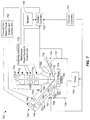
- FIG. 7 depicts an exemplary dual beam SEM/FIB system 702 that is equipped to carry out embodiments of the present invention.
- Embodiments of the present invention can be used in a wide variety of applications where a low resistivity material is deposited onto a target surface of a substrate. Preparation and analysis of such a sample is typically performed in a dual beam electron beam/focused ion beam system such as the one now described. Suitable dual beam systems are commercially available, for example, from FEI Company, Hillsboro, Oregon, the present assignee. While an example of suitable hardware is provided below, the invention is not limited to being implemented in any particular type of hardware.
- Dual beam system 702 has a vertically mounted electron beam column 704 and a focused ion beam (FIB) column 706 mounted at an angle of approximately 52 degrees from the vertical on an evacuable specimen chamber 708.
- the specimen chamber may be evacuated by pump system 709, which typically includes one or more, or a combination of, a turbo-molecular pump, oil diffusion pumps, ion getter pumps, scroll pumps, or other known pumping means.
- the electron beam column 704 includes an electron source 710, such as a Schottky emitter or a cold field emitter, for producing electrons, and electron-optical lenses 712 and 714 forming a finely focused beam of electrons 716.
- Electron source 710 is typically maintained at an electrical potential of between 500 V and 30 kV above the electrical potential of a work piece 718, which is typically maintained at ground potential.
- Work piece 718 may comprise, for example, a semiconductor device, microelectromechanical system (MEMS), data storage device, or a sample of material being analyzed for its material characteristics or composition.
- MEMS microelectromechanical system
- the impact point of the beam of electrons 716 can be positioned on and scanned over the surface of a work piece 718 by means of deflection coils 720. Operation of lenses 712 and 714 and deflection coils 720 is controlled by scanning electron microscope power supply and control unit 722. Lenses and deflection unit may use electric fields, magnetic fields, or a combination thereof.
- Work piece 718 is on movable stage 724 within specimen chamber 708.
- Stage 724 can preferably move in a horizontal plane (X-axis and Y-axis) and vertically (Z-axis) and can tilt approximately sixty (60) degrees and rotate about the Z-axis.
- a door 727 can be opened for inserting work piece 718 onto X-Y-Z stage 724 and also for servicing an internal gas supply reservoir (not shown), if one is used. The door is interlocked so that it cannot be opened if specimen chamber 708 is evacuated.
- Each GIS may comprises a reservoir (not shown) for holding the precursor or activation materials and a needle 732 for directing the gas to the surface of the work piece.
- Each GIS further comprises means 734 for regulating the supply of precursor material to the work piece.
- the regulating means are depicted as an adjustable valve, but the regulating means could also comprise, for example, a regulated heater for heating the precursor material to control its vapor pressure.
- Secondary electrons are detected by secondary electron detector 736, such as an Everhart-Thornley detector, or a semiconductor detector device capable of detecting low energy electrons.
- STEM detector 762 located beneath the TEM sample holder 761 and the stage 724, can collect electrons that are transmitted through a sample mounted on the TEM sample holder. Signals from the detectors 736, 762 are provided to a system controller 738. Said controller 738 also controls the deflector signals, lenses, electron source, GIS, stage and pump, and other items of the instrument. Monitor 740 is used to display user controls and an image of the work piece using the signal
- the chamber 708 is evacuated by pump system 709 under the control of vacuum controller 741.
- the vacuum system provides within chamber 708 a vacuum of approximately 7 x 10⁻⁶ mbar.
- the chamber background pressure may rise, typically to about 5 x 10⁻⁵ mbar.
- Focused ion beam column 706 comprises an upper neck portion 744 within which are located an ion source 746 and a focusing column 748 including extractor electrode 750 and an electrostatic optical system including an objective lens 751.
- Ion source 746 may comprise a liquid metal gallium ion source, a plasma ion source, a liquid metal alloy source, or any other type of ion source.
- the axis of focusing column 748 is tilted 52 degrees from the axis of the electron column.
- An ion beam 752 passes from ion source 746 through focusing column 748 and between electrostatic deflectors 754 toward work piece 718.
- FIB power supply and control unit 756 provides an electrical potential at ion source 746.
- Ion source 746 is typically maintained at an electrical potential of between 1 kV and 60 kV above the electrical potential of the work piece, which is typically maintained at ground potential.
- ions impact the work piece at landing energies of approximately 1 keV to 60 keV.
- FIB power supply and control unit 756 is coupled to deflection plates 754 which can cause the ion beam to trace out a corresponding pattern on the upper surface of work piece 718. In some systems, the deflection plates are placed before the final lens, as is well known in the art.
- the ion source 746 typically provides a beam of singly charged positive gallium ions that can be focused into a sub one-tenth micrometer wide beam at work piece 718 for modifying the work piece 718 by ion milling, enhanced etch, material deposition, or for imaging the work piece 718.
- a micromanipulator 757 such as the AutoProbe 200TM from Omniprobe, Inc., Dallas, Texas, or the Model MM3A from Kleindiek Nanotechnik, Reutlingen, Germany, can precisely move objects within the vacuum chamber.
- Micromanipulator 757 may comprise precision electric motors 758 positioned outside the vacuum chamber to provide X, Y, Z, and theta control of a portion 759 positioned within the vacuum chamber.
- the micromanipulator 757 can be fitted with different end effectors for manipulating small objects.
- the end effector is a thin probe 760.
- a micromanipulator or microprobe
- a micromanipulator can be used to transfer a TEM sample (which has been freed from a substrate, typically by an ion beam) to a TEM sample holder 761 for analysis.
- System controller 738 controls the operations of the various parts of dual beam system 702. Through system controller 738, a user can cause ion beam 752 or electron beam 716 to be scanned in a desired manner through commands entered into a conventional user interface (not shown). Alternatively, system controller 738 may control dual beam system 702 in accordance with programmed instructions.
- FIG. 7 is a schematic representation, which does not include all the elements of a typical dual beam system and which does not reflect the actual appearance and size of, or the relationship between, all the elements.
- embodiments of the present invention can be implemented via computer hardware, a combination of both hardware and software, or by computer instructions stored in a non-transitory computer-readable memory.
- the methods can be implemented in computer programs using standard programming techniques-including a non-transitory computer-readable storage medium configured with a computer program, where the storage medium so configured causes a computer to operate in a specific and predefined manner-according to the methods and figures described in this Specification.
- Each program may be implemented in a high level procedural or object oriented programming language to communicate with a computer system.
- the programs can be implemented in assembly or machine language, if desired. In any case, the language can be a compiled or interpreted language.
- the program can run on dedicated integrated circuits programmed for that purpose.
- methodologies may be implemented in any type of computing platform, including but not limited to, personal computers, mini-computers, main-frames, workstations, networked or distributed computing environments, computer platforms separate, integral to, or in communication with charged particle tools or other imaging devices, and the like.
- Aspects of the present invention may be implemented in machine readable code stored on a storage medium or device, whether removable or integral to the computing platform, such as a hard disc, optical read and/or write storage mediums, RAM, ROM, and the like, so that it is readable by a programmable computer, for configuring and operating the computer when the storage media or device is read by the computer to perform the procedures described herein.
- machine-readable code, or portions thereof may be transmitted over a wired or wireless network.
- the invention described herein includes these and other various types of computer-readable storage media when such media contain instructions or programs for implementing the steps described above in conjunction with a microprocessor or other data processor.
- the invention also includes the computer itself when programmed according to the methods and techniques described herein.
- Computer programs can be applied to input data to perform the functions described herein and thereby transform the input data to generate output data.
- the output information is applied to one or more output devices such as a display monitor.
- the transformed data represents physical and tangible objects, including producing a particular visual depiction of the physical and tangible objects on a display.
- Preferred embodiments of the present invention also make use of a particle beam apparatus, such as a FIB or SEM, in order to image a sample using a beam of particles.
- a particle beam apparatus such as a FIB or SEM
- Such particles used to image a sample inherently interact with the sample resulting in some degree of physical transformation.
- discussions utilizing terms such as “calculating,” “determining,” “measuring,” “generating,” “detecting,” “forming,” or the like also refer to the action and processes of a computer system, or similar electronic device, that manipulates and transforms data represented as physical quantities within the computer system into other data similarly represented as physical quantities within the computer system or other information storage, transmission or display devices.
- the invention has broad applicability and can provide many benefits as described and shown above.
- the embodiments will vary greatly depending upon the specific application, and not every embodiment will provide all of the benefits and meet all of the objectives that are achievable by the invention.
- Particle beam systems suitable for carrying out the present invention are commercially available, for example, from FEI Company, the present assignee.
- the invention could be applied to any suitable substrate or surface. Further, the present invention could be applied to samples that are thinned in the vacuum chamber but removed from the substrate outside the vacuum chamber (ex-situ-type samples) or to samples extracted from the substrate and thinned after mounting on a TEM grid inside the vacuum chamber ( in-situ-type samples). Whenever the terms "automatic,” “automated,” or similar terms are used herein, those terms will be understood to include manual initiation of the automatic or automated process or step.
- integrated circuit refers to a set of electronic components and their interconnections (internal electrical circuit elements, collectively) that are patterned on the surface of a microchip.
- semiconductor device refers generically to an integrated circuit (IC), which may be integral to a semiconductor wafer, singulated from a wafer, or packaged for use on a circuit board.
- FIB focused ion beam
- FIB focused ion beam
Claims (12)
- Verfahren zur Herstellung einer Probe für die TEM-Analyse, wobei das Verfahren aufweist:wenigstens teilweises Trennen (306) eines Probenschnitts, der ein Merkmal von Interesse enthält, von einer Substratmasse;Dünnermachen einer ersten Seite (308) der Probe, um eine erste Probenfläche freizulegen; undDünnermachen einer zweiten Seite (314) der Probe;Abscheiden einer Schicht aus einem Material (310) auf der freiliegenden Probenfläche, wobei die Schritte des Dünnermachens einer Seite der Probe, um eine Probenfläche freizulegen, und des Abscheidens einer Schicht aus einem Material auf diese freiliegende Probenfläche gleichzeitig durchgeführt werden;dadurch gekennzeichnet, dass das gleichzeitige Abscheiden und Dünnermachen durch einen fokussierten Ionenstrahl durchgeführt werden, wobei das Dünnermachen durch Ionenstrahlfräsen stattfindet und das Abscheiden durch Ionenstrahlinduzierte Zersetzung eines Vorläufergases stattfindet.
- Verfahren nach Anspruch 1, das ferner das Abscheiden einer Schicht aus einem Material auf die freiliegende zweite Probenfläche aufweist.
- Verfahren nach einem der vorhergehenden Ansprüche, das ferner das Wiederholen der Schritte des Verdünnens einer ersten Seite der Probe und des Abscheidens einer Schicht aus einem Material auf der freiliegenden ersten Probenfläche, bis eine gewünschte Endprobenfläche freiliegt, aufweist.
- Verfahren nach einem der vorhergehenden Ansprüche, das ferner das Entfernen wenigstens eines Abschnitts des abgeschiedenen Materials aufweist.
- Verfahren nach Anspruch 4, wobei das Entfernen wenigstens eines Abschnitts des abgeschiedenen Materials das Entfernen wenigstens eines Abschnitts des abgeschiedenen Materials durch ein anderes Verfahren als Ionenstrahlfräsen aufweist.
- Verfahren nach Anspruch 4, wobei das Entfernen wenigstens eines Abschnitts des abgeschiedenen Materials das Entfernen wenigstens eines Abschnitts des abgeschiedenen Materials durch gasunterstütztes Ätzen aufweist.
- Verfahren nach Anspruch 4, wobei das Dünnermachen in einer Vakuumkammer stattfindet und das Entfernen wenigstens eines Abschnitts des abgeschiedenen Materials das Entfernen wenigstens eines Abschnitts des abgeschiedenen Materials, nachdem die Probe aus der Vakuumkammer entfernt wurde, aufweist.
- Verfahren nach einem der Ansprüche 1 - 7, wobei die TEM-Endprobe 30 nm oder weniger dick ist.
- Verfahren nach einem der Ansprüche 1 - 7, wobei die Probe aus einer Mischung von Material mit einer höheren Ionenstrahlfräsgeschwindigkeit und einem Material mit einer niedrigeren Ionenstrahlfräsgeschwindigkeit zusammengesetzt ist.
- Verfahren nach einem der Ansprüche 1 - 7, wobei das Abscheiden einer Schicht aus einem Material (310) auf der freiliegenden ersten Probenfläche die vorherrschende Reaktion ist, die an entlegenen Abschnitten mit niedrigerem Strom des Strahls (752) stattfindet, und das Dünnermachen der Probe die vorherrschende Reaktion ist, die an Abschnitten mit hohem Strom in der Mitte des Strahls (752) stattfindet.
- Vorrichtung (702) zur Herstellung einer Probe (718) für die TEM-Analyse, die aufweist:ein Gestell (724) zum Halten einer Probe (718);eine Ionenquelle (746) zum Erzeugen eines Ionenstrahls (752);ein Gaseinspritzsystem (730), um ein Vorläufergas auf die Probe (718) zu richten;eine Steuerung (738) zum Steuern verschiedener Betriebe in der Vorrichtung (702), wobei die Steuerung (738) konfiguriert ist, um den Ionenstrahl (752) zu steuern, um die Schritte des Dünnermachens einer Seite der Probe (718), um eine Probenfläche freizulegen, und des Abscheidens einer Schicht aus einem Material auf dieser freiliegenden Fläche gleichzeitig durchzuführen, wobei das Dünnermachen durch Ionenstrahlfräsen durchgeführt wird und das Abscheiden durch Ionenstrahl-induzierte Zersetzung des Vorläufergases durchgeführt wird, um das Verfahren nach einem der vorhergehenden Ansprüche auszuführen.
- Nicht-flüchtiges computerlesbares Speichermedium, das mit einem Computerprogramm konfiguriert ist, wobei das derart konfigurierte Speichermedium bewirkt, dass ein Computer ein Ladungsträgerstrahlsystem steuert, um die Schritte des Verfahrens nach einem der Ansprüche 1 - 7 auszuführen.
Applications Claiming Priority (1)
| Application Number | Priority Date | Filing Date | Title |
|---|---|---|---|
| US201161493308P | 2011-06-03 | 2011-06-03 |
Publications (3)
| Publication Number | Publication Date |
|---|---|
| EP2530700A2 EP2530700A2 (de) | 2012-12-05 |
| EP2530700A3 EP2530700A3 (de) | 2014-02-26 |
| EP2530700B1 true EP2530700B1 (de) | 2017-03-01 |
Family
ID=46458147
Family Applications (1)
| Application Number | Title | Priority Date | Filing Date |
|---|---|---|---|
| EP12170383.9A Active EP2530700B1 (de) | 2011-06-03 | 2012-06-01 | Verfahren zur Herstellung dünner Proben zur TEM-Abbildung |
Country Status (4)
| Country | Link |
|---|---|
| US (2) | US8859963B2 (de) |
| EP (1) | EP2530700B1 (de) |
| JP (1) | JP6366216B2 (de) |
| CN (1) | CN102809496B (de) |
Families Citing this family (48)
| Publication number | Priority date | Publication date | Assignee | Title |
|---|---|---|---|---|
| US8859998B2 (en) | 2011-01-28 | 2014-10-14 | Fei Company | TEM sample preparation |
| US8912490B2 (en) | 2011-06-03 | 2014-12-16 | Fei Company | Method for preparing samples for imaging |
| EP2749863A3 (de) * | 2012-12-31 | 2016-05-04 | Fei Company | Verfahren zur Vorbereitung von Proben für Bildgebung |
| WO2013082496A1 (en) | 2011-12-01 | 2013-06-06 | Fei Company | High throughput tem preparation processes and hardware for backside thinning of cross-sectional view lamella |
| JP6105204B2 (ja) * | 2012-02-10 | 2017-03-29 | 株式会社日立ハイテクサイエンス | Tem観察用試料作製方法 |
| DE102012202519A1 (de) * | 2012-02-17 | 2013-08-22 | Carl Zeiss Microscopy Gmbh | Verfahren und Vorrichtungen zur Präparation mikroskopischer Proben mit Hilfe von gepulstem Licht |
| JP6085150B2 (ja) * | 2012-03-16 | 2017-02-22 | 株式会社日立ハイテクサイエンス | 試料作製装置及び試料作製方法 |
| JP5986408B2 (ja) * | 2012-03-22 | 2016-09-06 | 株式会社日立ハイテクサイエンス | 試料作製方法 |
| US10465293B2 (en) * | 2012-08-31 | 2019-11-05 | Fei Company | Dose-based end-pointing for low-kV FIB milling TEM sample preparation |
| JP6199978B2 (ja) * | 2012-10-05 | 2017-09-20 | エフ・イ−・アイ・カンパニー | 高アスペクト比構造体の分析 |
| KR20200011611A (ko) | 2012-10-05 | 2020-02-03 | 에프이아이 컴파니 | 하전 입자 빔 샘플 준비과정에서 커트닝을 감소하기 위한 방법 및 시스템 |
| JP6199979B2 (ja) * | 2012-10-05 | 2017-09-20 | エフ・イ−・アイ・カンパニー | 傾斜ミリング保護のためのバルク付着 |
| EP2939261B1 (de) * | 2012-12-31 | 2016-08-24 | FEI Company | Aufbringen von material in strukturen mit hohem aspektverhältnis |
| JP6629596B2 (ja) * | 2013-01-11 | 2020-01-15 | エフ・イ−・アイ・カンパニー | エッチング速度を変化させるためのイオン注入 |
| CN103940643A (zh) * | 2013-01-18 | 2014-07-23 | 中芯国际集成电路制造(上海)有限公司 | Tsv样品的制备方法 |
| CN103196718B (zh) * | 2013-03-14 | 2015-06-17 | 上海华力微电子有限公司 | Tem样品的制备方法 |
| CN103196728B (zh) * | 2013-04-09 | 2015-12-02 | 上海华力微电子有限公司 | 使用fib技术制备sem或tem样品保护层的方法 |
| CN103257066B (zh) * | 2013-05-07 | 2015-05-20 | 上海华力微电子有限公司 | Tem样品的制备方法 |
| CN103308365A (zh) * | 2013-06-27 | 2013-09-18 | 上海华力微电子有限公司 | Tem样品的制备方法 |
| JP6453580B2 (ja) * | 2013-08-14 | 2019-01-16 | エフ・イ−・アイ・カンパニー | 試料調製中におけるtem試料からのプローブの分離 |
| CN103743608B (zh) * | 2014-01-21 | 2016-01-20 | 东南大学 | 用于原位透射电子显微镜的深亚微米器件样品及制备方法 |
| US9552958B2 (en) * | 2014-02-25 | 2017-01-24 | Weatherford Technology Holdings, Llc | Alignment marking for rock sample analysis |
| CN103868773A (zh) * | 2014-03-24 | 2014-06-18 | 上海华力微电子有限公司 | 透射电镜样品的制作方法 |
| CN103868777B (zh) * | 2014-03-31 | 2016-03-02 | 上海华力微电子有限公司 | 透射电镜样品的制备方法 |
| US20150369710A1 (en) * | 2014-06-24 | 2015-12-24 | Fei Company | Method and System of Creating a Symmetrical FIB Deposition |
| CN105334086A (zh) * | 2014-08-13 | 2016-02-17 | 中芯国际集成电路制造(上海)有限公司 | Tem样品的制备方法及tem样品 |
| KR102358551B1 (ko) * | 2014-08-29 | 2022-02-04 | 가부시키가이샤 히다치 하이테크 사이언스 | 자동 시료편 제작 장치 |
| CN105510092B (zh) * | 2014-09-22 | 2019-11-01 | 中芯国际集成电路制造(上海)有限公司 | Tem样品的制备方法 |
| CN105092330B (zh) * | 2015-08-12 | 2017-12-22 | 上海华力微电子有限公司 | 一种tem样品制备方法 |
| US9978586B2 (en) * | 2015-11-06 | 2018-05-22 | Fei Company | Method of material deposition |
| CN105699139B (zh) * | 2016-01-20 | 2019-04-23 | 西安电子科技大学 | 基于反应离子刻蚀的GaN薄膜透射电子显微镜截面样品制备方法 |
| US9837246B1 (en) | 2016-07-22 | 2017-12-05 | Fei Company | Reinforced sample for transmission electron microscope |
| KR101737946B1 (ko) | 2016-08-16 | 2017-05-19 | 서울대학교산학협력단 | 박막 물성측정 및 분석용 시료 제작 방법 및 이에 의해 제작된 시료 |
| CN107860620B (zh) * | 2016-09-22 | 2020-07-28 | 中芯国际集成电路制造(上海)有限公司 | 一种透射电子显微镜样品及其制备方法 |
| CN106814095B (zh) * | 2017-02-12 | 2019-05-24 | 马新军 | 用于扫描电镜的冷冻制样装置 |
| US10324049B2 (en) | 2017-02-15 | 2019-06-18 | Saudi Arabian Oil Company | Rock sample preparation method by using focused ion beam for minimizing curtain effect |
| JP6974820B2 (ja) * | 2017-03-27 | 2021-12-01 | 株式会社日立ハイテクサイエンス | 荷電粒子ビーム装置、試料加工方法 |
| US10546719B2 (en) * | 2017-06-02 | 2020-01-28 | Fei Company | Face-on, gas-assisted etching for plan-view lamellae preparation |
| DE102017212020B3 (de) | 2017-07-13 | 2018-05-30 | Carl Zeiss Microscopy Gmbh | Verfahren zur In-situ-Präparation und zum Transfer mikroskopischer Proben, Computerprogrammprodukt sowie mikroskopische Probe |
| CN108036979B (zh) * | 2017-11-15 | 2018-12-21 | 中国科学院地质与地球物理研究所 | 基于静电力的矿物样品靶及其制作方法 |
| KR102537699B1 (ko) | 2017-12-26 | 2023-05-26 | 삼성전자주식회사 | 반도체 장치의 검사 방법 |
| CN110530700B (zh) * | 2019-10-14 | 2022-04-12 | 长江存储科技有限责任公司 | 采用fib制备测试样品的方法以及测试样品 |
| CN111366428B (zh) * | 2020-03-03 | 2023-06-09 | 上海华力集成电路制造有限公司 | Fib倒切制备tem样品的方法 |
| US11069509B1 (en) * | 2020-03-16 | 2021-07-20 | Fei Company | Method and system for backside planar view lamella preparation |
| CN113834831B (zh) * | 2020-06-08 | 2023-07-21 | 全德科技(厦门)有限公司 | 制备透射电子显微镜样品的方法 |
| CN112041671B (zh) * | 2020-07-24 | 2023-10-20 | 长江存储科技有限责任公司 | 制备和分析薄膜的方法 |
| CN113588372B (zh) * | 2021-08-13 | 2022-09-02 | 胜科纳米(苏州)股份有限公司 | 测量vcsel器件多层膜元素扩散的样品制备方法以及检测方法 |
| CN115078431A (zh) * | 2022-06-16 | 2022-09-20 | 中国核动力研究设计院 | 一种基于自离子辐照后锆合金透射电镜试样制备方法 |
Family Cites Families (28)
| Publication number | Priority date | Publication date | Assignee | Title |
|---|---|---|---|---|
| JPH1158033A (ja) | 1997-08-26 | 1999-03-02 | Nippon Telegr & Teleph Corp <Ntt> | イオンミリング方法 |
| US6042736A (en) | 1997-11-17 | 2000-03-28 | Taiwan Semiconductor Manufacturing Co., Ltd. | Method for preparing samples for microscopic examination |
| US6039000A (en) | 1998-02-11 | 2000-03-21 | Micrion Corporation | Focused particle beam systems and methods using a tilt column |
| JP2000035391A (ja) * | 1998-07-16 | 2000-02-02 | Seiko Instruments Inc | 薄片化加工時の試料歪除去方法 |
| JP2004537758A (ja) * | 2001-07-27 | 2004-12-16 | エフ・イ−・アイ・カンパニー | 電子ビーム処理 |
| JP3735614B2 (ja) | 2003-03-19 | 2006-01-18 | 株式会社東芝 | 透過電子顕微鏡観測用下地試料、透過電子顕微鏡測定方法、および透過電子顕微鏡装置 |
| US7611610B2 (en) * | 2003-11-18 | 2009-11-03 | Fei Company | Method and apparatus for controlling topographical variation on a milled cross-section of a structure |
| US7442924B2 (en) * | 2005-02-23 | 2008-10-28 | Fei, Company | Repetitive circumferential milling for sample preparation |
| JP2007092507A (ja) | 2005-09-05 | 2007-04-12 | Hitachi Zosen Corp | ジェットフローゲート |
| JP4947965B2 (ja) * | 2005-12-06 | 2012-06-06 | ラピスセミコンダクタ株式会社 | 透過型電子顕微鏡用の試料の作製方法、観察方法及び構造 |
| JP5600371B2 (ja) | 2006-02-15 | 2014-10-01 | エフ・イ−・アイ・カンパニー | 荷電粒子ビーム処理のための保護層のスパッタリング・コーティング |
| JP2007292507A (ja) * | 2006-04-21 | 2007-11-08 | Matsushita Electric Ind Co Ltd | 透過型電子顕微鏡の試料作製方法および集束イオンビーム装置 |
| US7423263B2 (en) * | 2006-06-23 | 2008-09-09 | Fei Company | Planar view sample preparation |
| JP5410286B2 (ja) | 2006-10-20 | 2014-02-05 | エフ・イ−・アイ・カンパニー | S/temのサンプルを作成する方法およびサンプル構造 |
| US8835880B2 (en) * | 2006-10-31 | 2014-09-16 | Fei Company | Charged particle-beam processing using a cluster source |
| EP2109873B1 (de) * | 2007-02-06 | 2017-04-05 | FEI Company | Geladenes teilchenstrahlsystem unter hochdruck |
| US8835845B2 (en) | 2007-06-01 | 2014-09-16 | Fei Company | In-situ STEM sample preparation |
| EP2009421A1 (de) | 2007-06-29 | 2008-12-31 | FEI Company | Verfahren zum Abtrennen einer Lamelle aus einer Bohrprobe zur TEM-Prüfung |
| JP5017059B2 (ja) * | 2007-10-29 | 2012-09-05 | エスアイアイ・ナノテクノロジー株式会社 | 試料作成装置および試料姿勢転換方法 |
| JP2009198412A (ja) | 2008-02-25 | 2009-09-03 | Sii Nanotechnology Inc | 透過電子顕微鏡用試料の作製方法及び透過電子顕微鏡用試料 |
| US8278220B2 (en) * | 2008-08-08 | 2012-10-02 | Fei Company | Method to direct pattern metals on a substrate |
| CN101776543A (zh) * | 2009-01-13 | 2010-07-14 | 中芯国际集成电路制造(上海)有限公司 | 透射电子显微镜检测样片的制备方法 |
| US8778804B2 (en) * | 2009-01-30 | 2014-07-15 | Fei Company | High selectivity, low damage electron-beam delineation etch |
| EP2226830B1 (de) * | 2009-03-06 | 2014-01-08 | FEI Company | Berarbeitung mit einem geladenen Teilchenstrahl |
| EP2233907A1 (de) * | 2009-03-27 | 2010-09-29 | FEI Company | Erzeugung eines Bildes während des Fräsens eines Werkstücks |
| WO2011060444A2 (en) * | 2009-11-16 | 2011-05-19 | Fei Company | Gas delivery for beam processing systems |
| EP2402475A1 (de) * | 2010-06-30 | 2012-01-04 | Fei Company | Strahleninduzierte Ablagerung bei kryogenischen Temperaturen |
| US8859998B2 (en) | 2011-01-28 | 2014-10-14 | Fei Company | TEM sample preparation |
-
2012
- 2012-05-25 US US13/481,351 patent/US8859963B2/en active Active
- 2012-05-31 JP JP2012124150A patent/JP6366216B2/ja active Active
- 2012-06-01 CN CN201210178011.XA patent/CN102809496B/zh active Active
- 2012-06-01 EP EP12170383.9A patent/EP2530700B1/de active Active
-
2014
- 2014-10-14 US US14/514,199 patent/US9279752B2/en active Active
Non-Patent Citations (1)
| Title |
|---|
| RAI R S ET AL: "Role of transmission electron microscopy in the semiconductor industry for process development and failure analysis", PROGRESS IN CRYSTAL GROWTH AND CHARACTERIZATION OF MATERIALS, ELSEVIER PUBLISHING, BARKING, GB, vol. 55, no. 3-4, 1 September 2009 (2009-09-01), pages 63 - 97, XP026770762, ISSN: 0960-8974, [retrieved on 20091102], DOI: 10.1016/J.PCRYSGROW.2009.09.002 * |
Also Published As
| Publication number | Publication date |
|---|---|
| CN102809496B (zh) | 2016-09-07 |
| US20130143412A1 (en) | 2013-06-06 |
| US8859963B2 (en) | 2014-10-14 |
| CN102809496A (zh) | 2012-12-05 |
| EP2530700A3 (de) | 2014-02-26 |
| US20150102009A1 (en) | 2015-04-16 |
| US9279752B2 (en) | 2016-03-08 |
| JP6366216B2 (ja) | 2018-08-01 |
| JP2012252004A (ja) | 2012-12-20 |
| EP2530700A2 (de) | 2012-12-05 |
Similar Documents
| Publication | Publication Date | Title |
|---|---|---|
| EP2530700B1 (de) | Verfahren zur Herstellung dünner Proben zur TEM-Abbildung | |
| US9111720B2 (en) | Method for preparing samples for imaging | |
| EP2749863A2 (de) | Verfahren zur Vorbereitung von Proben für Bildgebung | |
| US8822921B2 (en) | Method for preparing samples for imaging | |
| US9378925B2 (en) | TEM sample preparation | |
| EP1998356B1 (de) | In-Situ-STEM-Probenherstellung | |
| EP2704179B1 (de) | Dosisbasierte Endpunktbestimung für das Nieder-kV-FIB-Ätzen bei der TEM-Probenherstellung | |
| JP6224612B2 (ja) | 断面観察薄片の裏側薄化用の高スループットtem調製プロセスおよびハードウェア | |
| JP2015517676A (ja) | Tem観察用の薄片の調製 | |
| JP2014130145A5 (de) | ||
| EP2960924A1 (de) | Verfahren und system zur erzeugung von symmetrischer fib-abscheidung | |
| US10053768B2 (en) | Detaching probe from TEM sample during sample preparation |
Legal Events
| Date | Code | Title | Description |
|---|---|---|---|
| PUAI | Public reference made under article 153(3) epc to a published international application that has entered the european phase |
Free format text: ORIGINAL CODE: 0009012 |
|
| AK | Designated contracting states |
Kind code of ref document: A2 Designated state(s): AL AT BE BG CH CY CZ DE DK EE ES FI FR GB GR HR HU IE IS IT LI LT LU LV MC MK MT NL NO PL PT RO RS SE SI SK SM TR |
|
| AX | Request for extension of the european patent |
Extension state: BA ME |
|
| PUAL | Search report despatched |
Free format text: ORIGINAL CODE: 0009013 |
|
| AK | Designated contracting states |
Kind code of ref document: A3 Designated state(s): AL AT BE BG CH CY CZ DE DK EE ES FI FR GB GR HR HU IE IS IT LI LT LU LV MC MK MT NL NO PL PT RO RS SE SI SK SM TR |
|
| AX | Request for extension of the european patent |
Extension state: BA ME |
|
| RIC1 | Information provided on ipc code assigned before grant |
Ipc: H01L 21/02 20060101ALI20140121BHEP Ipc: G01N 1/28 20060101ALI20140121BHEP Ipc: H01J 37/305 20060101AFI20140121BHEP |
|
| 17P | Request for examination filed |
Effective date: 20140820 |
|
| RBV | Designated contracting states (corrected) |
Designated state(s): AL AT BE BG CH CY CZ DE DK EE ES FI FR GB GR HR HU IE IS IT LI LT LU LV MC MK MT NL NO PL PT RO RS SE SI SK SM TR |
|
| 17Q | First examination report despatched |
Effective date: 20160104 |
|
| GRAP | Despatch of communication of intention to grant a patent |
Free format text: ORIGINAL CODE: EPIDOSNIGR1 |
|
| GRAJ | Information related to disapproval of communication of intention to grant by the applicant or resumption of examination proceedings by the epo deleted |
Free format text: ORIGINAL CODE: EPIDOSDIGR1 |
|
| INTG | Intention to grant announced |
Effective date: 20161004 |
|
| INTG | Intention to grant announced |
Effective date: 20161019 |
|
| GRAP | Despatch of communication of intention to grant a patent |
Free format text: ORIGINAL CODE: EPIDOSNIGR1 |
|
| INTC | Intention to grant announced (deleted) | ||
| INTG | Intention to grant announced |
Effective date: 20161202 |
|
| GRAS | Grant fee paid |
Free format text: ORIGINAL CODE: EPIDOSNIGR3 |
|
| GRAA | (expected) grant |
Free format text: ORIGINAL CODE: 0009210 |
|
| AK | Designated contracting states |
Kind code of ref document: B1 Designated state(s): AL AT BE BG CH CY CZ DE DK EE ES FI FR GB GR HR HU IE IS IT LI LT LU LV MC MK MT NL NO PL PT RO RS SE SI SK SM TR |
|
| REG | Reference to a national code |
Ref country code: GB Ref legal event code: FG4D |
|
| REG | Reference to a national code |
Ref country code: CH Ref legal event code: EP Ref country code: AT Ref legal event code: REF Ref document number: 872218 Country of ref document: AT Kind code of ref document: T Effective date: 20170315 |
|
| REG | Reference to a national code |
Ref country code: IE Ref legal event code: FG4D |
|
| REG | Reference to a national code |
Ref country code: DE Ref legal event code: R096 Ref document number: 602012029125 Country of ref document: DE |
|
| REG | Reference to a national code |
Ref country code: NL Ref legal event code: MP Effective date: 20170301 |
|
| REG | Reference to a national code |
Ref country code: LT Ref legal event code: MG4D |
|
| REG | Reference to a national code |
Ref country code: AT Ref legal event code: MK05 Ref document number: 872218 Country of ref document: AT Kind code of ref document: T Effective date: 20170301 |
|
| PG25 | Lapsed in a contracting state [announced via postgrant information from national office to epo] |
Ref country code: GR Free format text: LAPSE BECAUSE OF FAILURE TO SUBMIT A TRANSLATION OF THE DESCRIPTION OR TO PAY THE FEE WITHIN THE PRESCRIBED TIME-LIMIT Effective date: 20170602 Ref country code: FI Free format text: LAPSE BECAUSE OF FAILURE TO SUBMIT A TRANSLATION OF THE DESCRIPTION OR TO PAY THE FEE WITHIN THE PRESCRIBED TIME-LIMIT Effective date: 20170301 Ref country code: NO Free format text: LAPSE BECAUSE OF FAILURE TO SUBMIT A TRANSLATION OF THE DESCRIPTION OR TO PAY THE FEE WITHIN THE PRESCRIBED TIME-LIMIT Effective date: 20170601 Ref country code: HR Free format text: LAPSE BECAUSE OF FAILURE TO SUBMIT A TRANSLATION OF THE DESCRIPTION OR TO PAY THE FEE WITHIN THE PRESCRIBED TIME-LIMIT Effective date: 20170301 Ref country code: LT Free format text: LAPSE BECAUSE OF FAILURE TO SUBMIT A TRANSLATION OF THE DESCRIPTION OR TO PAY THE FEE WITHIN THE PRESCRIBED TIME-LIMIT Effective date: 20170301 |
|
| PG25 | Lapsed in a contracting state [announced via postgrant information from national office to epo] |
Ref country code: ES Free format text: LAPSE BECAUSE OF FAILURE TO SUBMIT A TRANSLATION OF THE DESCRIPTION OR TO PAY THE FEE WITHIN THE PRESCRIBED TIME-LIMIT Effective date: 20170301 Ref country code: SE Free format text: LAPSE BECAUSE OF FAILURE TO SUBMIT A TRANSLATION OF THE DESCRIPTION OR TO PAY THE FEE WITHIN THE PRESCRIBED TIME-LIMIT Effective date: 20170301 Ref country code: LV Free format text: LAPSE BECAUSE OF FAILURE TO SUBMIT A TRANSLATION OF THE DESCRIPTION OR TO PAY THE FEE WITHIN THE PRESCRIBED TIME-LIMIT Effective date: 20170301 Ref country code: RS Free format text: LAPSE BECAUSE OF FAILURE TO SUBMIT A TRANSLATION OF THE DESCRIPTION OR TO PAY THE FEE WITHIN THE PRESCRIBED TIME-LIMIT Effective date: 20170301 Ref country code: BG Free format text: LAPSE BECAUSE OF FAILURE TO SUBMIT A TRANSLATION OF THE DESCRIPTION OR TO PAY THE FEE WITHIN THE PRESCRIBED TIME-LIMIT Effective date: 20170601 Ref country code: AT Free format text: LAPSE BECAUSE OF FAILURE TO SUBMIT A TRANSLATION OF THE DESCRIPTION OR TO PAY THE FEE WITHIN THE PRESCRIBED TIME-LIMIT Effective date: 20170301 |
|
| PG25 | Lapsed in a contracting state [announced via postgrant information from national office to epo] |
Ref country code: NL Free format text: LAPSE BECAUSE OF FAILURE TO SUBMIT A TRANSLATION OF THE DESCRIPTION OR TO PAY THE FEE WITHIN THE PRESCRIBED TIME-LIMIT Effective date: 20170301 |
|
| PG25 | Lapsed in a contracting state [announced via postgrant information from national office to epo] |
Ref country code: CZ Free format text: LAPSE BECAUSE OF FAILURE TO SUBMIT A TRANSLATION OF THE DESCRIPTION OR TO PAY THE FEE WITHIN THE PRESCRIBED TIME-LIMIT Effective date: 20170301 Ref country code: IT Free format text: LAPSE BECAUSE OF FAILURE TO SUBMIT A TRANSLATION OF THE DESCRIPTION OR TO PAY THE FEE WITHIN THE PRESCRIBED TIME-LIMIT Effective date: 20170301 Ref country code: RO Free format text: LAPSE BECAUSE OF FAILURE TO SUBMIT A TRANSLATION OF THE DESCRIPTION OR TO PAY THE FEE WITHIN THE PRESCRIBED TIME-LIMIT Effective date: 20170301 Ref country code: SK Free format text: LAPSE BECAUSE OF FAILURE TO SUBMIT A TRANSLATION OF THE DESCRIPTION OR TO PAY THE FEE WITHIN THE PRESCRIBED TIME-LIMIT Effective date: 20170301 Ref country code: EE Free format text: LAPSE BECAUSE OF FAILURE TO SUBMIT A TRANSLATION OF THE DESCRIPTION OR TO PAY THE FEE WITHIN THE PRESCRIBED TIME-LIMIT Effective date: 20170301 |
|
| PG25 | Lapsed in a contracting state [announced via postgrant information from national office to epo] |
Ref country code: PL Free format text: LAPSE BECAUSE OF FAILURE TO SUBMIT A TRANSLATION OF THE DESCRIPTION OR TO PAY THE FEE WITHIN THE PRESCRIBED TIME-LIMIT Effective date: 20170301 Ref country code: PT Free format text: LAPSE BECAUSE OF FAILURE TO SUBMIT A TRANSLATION OF THE DESCRIPTION OR TO PAY THE FEE WITHIN THE PRESCRIBED TIME-LIMIT Effective date: 20170703 Ref country code: SM Free format text: LAPSE BECAUSE OF FAILURE TO SUBMIT A TRANSLATION OF THE DESCRIPTION OR TO PAY THE FEE WITHIN THE PRESCRIBED TIME-LIMIT Effective date: 20170301 Ref country code: IS Free format text: LAPSE BECAUSE OF FAILURE TO SUBMIT A TRANSLATION OF THE DESCRIPTION OR TO PAY THE FEE WITHIN THE PRESCRIBED TIME-LIMIT Effective date: 20170701 |
|
| REG | Reference to a national code |
Ref country code: DE Ref legal event code: R097 Ref document number: 602012029125 Country of ref document: DE |
|
| PLBE | No opposition filed within time limit |
Free format text: ORIGINAL CODE: 0009261 |
|
| STAA | Information on the status of an ep patent application or granted ep patent |
Free format text: STATUS: NO OPPOSITION FILED WITHIN TIME LIMIT |
|
| PG25 | Lapsed in a contracting state [announced via postgrant information from national office to epo] |
Ref country code: MC Free format text: LAPSE BECAUSE OF FAILURE TO SUBMIT A TRANSLATION OF THE DESCRIPTION OR TO PAY THE FEE WITHIN THE PRESCRIBED TIME-LIMIT Effective date: 20170301 Ref country code: DK Free format text: LAPSE BECAUSE OF FAILURE TO SUBMIT A TRANSLATION OF THE DESCRIPTION OR TO PAY THE FEE WITHIN THE PRESCRIBED TIME-LIMIT Effective date: 20170301 |
|
| REG | Reference to a national code |
Ref country code: CH Ref legal event code: PL |
|
| 26N | No opposition filed |
Effective date: 20171204 |
|
| GBPC | Gb: european patent ceased through non-payment of renewal fee |
Effective date: 20170601 |
|
| PG25 | Lapsed in a contracting state [announced via postgrant information from national office to epo] |
Ref country code: SI Free format text: LAPSE BECAUSE OF FAILURE TO SUBMIT A TRANSLATION OF THE DESCRIPTION OR TO PAY THE FEE WITHIN THE PRESCRIBED TIME-LIMIT Effective date: 20170301 |
|
| REG | Reference to a national code |
Ref country code: IE Ref legal event code: MM4A |
|
| REG | Reference to a national code |
Ref country code: FR Ref legal event code: ST Effective date: 20180228 |
|
| PG25 | Lapsed in a contracting state [announced via postgrant information from national office to epo] |
Ref country code: LU Free format text: LAPSE BECAUSE OF NON-PAYMENT OF DUE FEES Effective date: 20170601 Ref country code: IE Free format text: LAPSE BECAUSE OF NON-PAYMENT OF DUE FEES Effective date: 20170601 Ref country code: GB Free format text: LAPSE BECAUSE OF NON-PAYMENT OF DUE FEES Effective date: 20170601 Ref country code: CH Free format text: LAPSE BECAUSE OF NON-PAYMENT OF DUE FEES Effective date: 20170630 Ref country code: LI Free format text: LAPSE BECAUSE OF NON-PAYMENT OF DUE FEES Effective date: 20170630 |
|
| PG25 | Lapsed in a contracting state [announced via postgrant information from national office to epo] |
Ref country code: FR Free format text: LAPSE BECAUSE OF NON-PAYMENT OF DUE FEES Effective date: 20170630 |
|
| REG | Reference to a national code |
Ref country code: BE Ref legal event code: MM Effective date: 20170630 |
|
| PG25 | Lapsed in a contracting state [announced via postgrant information from national office to epo] |
Ref country code: BE Free format text: LAPSE BECAUSE OF NON-PAYMENT OF DUE FEES Effective date: 20170630 |
|
| PG25 | Lapsed in a contracting state [announced via postgrant information from national office to epo] |
Ref country code: MT Free format text: LAPSE BECAUSE OF NON-PAYMENT OF DUE FEES Effective date: 20170601 |
|
| PG25 | Lapsed in a contracting state [announced via postgrant information from national office to epo] |
Ref country code: HU Free format text: LAPSE BECAUSE OF FAILURE TO SUBMIT A TRANSLATION OF THE DESCRIPTION OR TO PAY THE FEE WITHIN THE PRESCRIBED TIME-LIMIT; INVALID AB INITIO Effective date: 20120601 |
|
| PG25 | Lapsed in a contracting state [announced via postgrant information from national office to epo] |
Ref country code: CY Free format text: LAPSE BECAUSE OF NON-PAYMENT OF DUE FEES Effective date: 20170301 |
|
| PG25 | Lapsed in a contracting state [announced via postgrant information from national office to epo] |
Ref country code: MK Free format text: LAPSE BECAUSE OF FAILURE TO SUBMIT A TRANSLATION OF THE DESCRIPTION OR TO PAY THE FEE WITHIN THE PRESCRIBED TIME-LIMIT Effective date: 20170301 |
|
| PG25 | Lapsed in a contracting state [announced via postgrant information from national office to epo] |
Ref country code: TR Free format text: LAPSE BECAUSE OF FAILURE TO SUBMIT A TRANSLATION OF THE DESCRIPTION OR TO PAY THE FEE WITHIN THE PRESCRIBED TIME-LIMIT Effective date: 20170301 |
|
| PG25 | Lapsed in a contracting state [announced via postgrant information from national office to epo] |
Ref country code: AL Free format text: LAPSE BECAUSE OF FAILURE TO SUBMIT A TRANSLATION OF THE DESCRIPTION OR TO PAY THE FEE WITHIN THE PRESCRIBED TIME-LIMIT Effective date: 20170301 |
|
| PGFP | Annual fee paid to national office [announced via postgrant information from national office to epo] |
Ref country code: DE Payment date: 20230616 Year of fee payment: 12 |