EP2476205B1 - Oscillator having negative resistance element - Google Patents
Oscillator having negative resistance element Download PDFInfo
- Publication number
- EP2476205B1 EP2476205B1 EP10749690.3A EP10749690A EP2476205B1 EP 2476205 B1 EP2476205 B1 EP 2476205B1 EP 10749690 A EP10749690 A EP 10749690A EP 2476205 B1 EP2476205 B1 EP 2476205B1
- Authority
- EP
- European Patent Office
- Prior art keywords
- capacitor
- negative resistance
- resistance element
- frequency
- capacitance
- Prior art date
- Legal status (The legal status is an assumption and is not a legal conclusion. Google has not performed a legal analysis and makes no representation as to the accuracy of the status listed.)
- Not-in-force
Links
- 239000003990 capacitor Substances 0.000 claims description 83
- 230000010355 oscillation Effects 0.000 claims description 57
- 239000000758 substrate Substances 0.000 claims description 23
- 230000003071 parasitic effect Effects 0.000 claims description 20
- 229910000530 Gallium indium arsenide Inorganic materials 0.000 description 12
- 229910001218 Gallium arsenide Inorganic materials 0.000 description 5
- 230000004888 barrier function Effects 0.000 description 5
- 230000000694 effects Effects 0.000 description 5
- 239000002184 metal Substances 0.000 description 5
- 229910052751 metal Inorganic materials 0.000 description 5
- 238000000034 method Methods 0.000 description 5
- 239000010408 film Substances 0.000 description 4
- 239000000463 material Substances 0.000 description 4
- 239000004065 semiconductor Substances 0.000 description 4
- 239000000126 substance Substances 0.000 description 4
- 239000010409 thin film Substances 0.000 description 4
- GWEVSGVZZGPLCZ-UHFFFAOYSA-N Titan oxide Chemical compound O=[Ti]=O GWEVSGVZZGPLCZ-UHFFFAOYSA-N 0.000 description 3
- 239000013078 crystal Substances 0.000 description 3
- 238000002347 injection Methods 0.000 description 3
- 239000007924 injection Substances 0.000 description 3
- NRNCYVBFPDDJNE-UHFFFAOYSA-N pemoline Chemical compound O1C(N)=NC(=O)C1C1=CC=CC=C1 NRNCYVBFPDDJNE-UHFFFAOYSA-N 0.000 description 3
- OGIDPMRJRNCKJF-UHFFFAOYSA-N titanium oxide Inorganic materials [Ti]=O OGIDPMRJRNCKJF-UHFFFAOYSA-N 0.000 description 3
- 230000005641 tunneling Effects 0.000 description 3
- 229910000980 Aluminium gallium arsenide Inorganic materials 0.000 description 2
- 238000000862 absorption spectrum Methods 0.000 description 2
- 230000008901 benefit Effects 0.000 description 2
- 230000005540 biological transmission Effects 0.000 description 2
- 239000000919 ceramic Substances 0.000 description 2
- 238000006243 chemical reaction Methods 0.000 description 2
- 230000007423 decrease Effects 0.000 description 2
- 238000013461 design Methods 0.000 description 2
- 239000003989 dielectric material Substances 0.000 description 2
- 238000003384 imaging method Methods 0.000 description 2
- 230000001678 irradiating effect Effects 0.000 description 2
- 230000009467 reduction Effects 0.000 description 2
- 125000006850 spacer group Chemical group 0.000 description 2
- 238000001228 spectrum Methods 0.000 description 2
- 230000001629 suppression Effects 0.000 description 2
- 239000010936 titanium Substances 0.000 description 2
- 229910002704 AlGaN Inorganic materials 0.000 description 1
- JMASRVWKEDWRBT-UHFFFAOYSA-N Gallium nitride Chemical compound [Ga]#N JMASRVWKEDWRBT-UHFFFAOYSA-N 0.000 description 1
- 239000004698 Polyethylene Substances 0.000 description 1
- 239000004642 Polyimide Substances 0.000 description 1
- 229910000577 Silicon-germanium Inorganic materials 0.000 description 1
- PNEYBMLMFCGWSK-UHFFFAOYSA-N aluminium oxide Inorganic materials [O-2].[O-2].[O-2].[Al+3].[Al+3] PNEYBMLMFCGWSK-UHFFFAOYSA-N 0.000 description 1
- 238000004458 analytical method Methods 0.000 description 1
- JRPBQTZRNDNNOP-UHFFFAOYSA-N barium titanate Chemical compound [Ba+2].[Ba+2].[O-][Ti]([O-])([O-])[O-] JRPBQTZRNDNNOP-UHFFFAOYSA-N 0.000 description 1
- 229910002113 barium titanate Inorganic materials 0.000 description 1
- UMIVXZPTRXBADB-UHFFFAOYSA-N benzocyclobutene Chemical compound C1=CC=C2CCC2=C1 UMIVXZPTRXBADB-UHFFFAOYSA-N 0.000 description 1
- 230000008859 change Effects 0.000 description 1
- 239000011248 coating agent Substances 0.000 description 1
- 238000000576 coating method Methods 0.000 description 1
- 238000004891 communication Methods 0.000 description 1
- 150000001875 compounds Chemical class 0.000 description 1
- 229910052593 corundum Inorganic materials 0.000 description 1
- 238000011161 development Methods 0.000 description 1
- 238000005530 etching Methods 0.000 description 1
- 230000005284 excitation Effects 0.000 description 1
- 230000006872 improvement Effects 0.000 description 1
- 230000007246 mechanism Effects 0.000 description 1
- 239000000203 mixture Substances 0.000 description 1
- 238000012986 modification Methods 0.000 description 1
- 230000004048 modification Effects 0.000 description 1
- 230000000704 physical effect Effects 0.000 description 1
- 239000004033 plastic Substances 0.000 description 1
- 229920003023 plastic Polymers 0.000 description 1
- -1 polyethylene Polymers 0.000 description 1
- 229920000573 polyethylene Polymers 0.000 description 1
- 229920001721 polyimide Polymers 0.000 description 1
- 229920000098 polyolefin Polymers 0.000 description 1
- 238000002360 preparation method Methods 0.000 description 1
- 230000001902 propagating effect Effects 0.000 description 1
- 230000001603 reducing effect Effects 0.000 description 1
- 238000011160 research Methods 0.000 description 1
- 239000011347 resin Substances 0.000 description 1
- 229920005989 resin Polymers 0.000 description 1
- 238000012306 spectroscopic technique Methods 0.000 description 1
- 230000006641 stabilisation Effects 0.000 description 1
- 238000011105 stabilization Methods 0.000 description 1
- 238000003325 tomography Methods 0.000 description 1
- 229910001845 yogo sapphire Inorganic materials 0.000 description 1
Images

Classifications
-
- H—ELECTRICITY
- H03—ELECTRONIC CIRCUITRY
- H03B—GENERATION OF OSCILLATIONS, DIRECTLY OR BY FREQUENCY-CHANGING, BY CIRCUITS EMPLOYING ACTIVE ELEMENTS WHICH OPERATE IN A NON-SWITCHING MANNER; GENERATION OF NOISE BY SUCH CIRCUITS
- H03B7/00—Generation of oscillations using active element having a negative resistance between two of its electrodes
- H03B7/02—Generation of oscillations using active element having a negative resistance between two of its electrodes with frequency-determining element comprising lumped inductance and capacitance
- H03B7/06—Generation of oscillations using active element having a negative resistance between two of its electrodes with frequency-determining element comprising lumped inductance and capacitance active element being semiconductor device
- H03B7/08—Generation of oscillations using active element having a negative resistance between two of its electrodes with frequency-determining element comprising lumped inductance and capacitance active element being semiconductor device being a tunnel diode
-
- H—ELECTRICITY
- H03—ELECTRONIC CIRCUITRY
- H03B—GENERATION OF OSCILLATIONS, DIRECTLY OR BY FREQUENCY-CHANGING, BY CIRCUITS EMPLOYING ACTIVE ELEMENTS WHICH OPERATE IN A NON-SWITCHING MANNER; GENERATION OF NOISE BY SUCH CIRCUITS
- H03B9/00—Generation of oscillations using transit-time effects
- H03B9/12—Generation of oscillations using transit-time effects using solid state devices, e.g. Gunn-effect devices
Definitions
- the present invention relates to an oscillator and, more particularly, to a current injection type oscillator oscillating an electromagnetic wave including at least a part thereof a frequency component in a frequency region from the millimeter wave band to the terahertz wave band (more than 30 GHz and not more than 30 THz). More detailedly, the present invention relates to a current injection type oscillator having a negative resistance element such as an element having a resonant tunneling diode structure.
- Non-destructive sensing techniques using electromagnetic waves in a frequency region from the millimeter wave band to the terahertz wave band (more than 30 GHz and not more than 30 THz) have been developed.
- Fields of application of electromagnetic waves of the frequency bands cover imaging techniques using safe fluoroscopic examination apparatus that replace X-ray apparatus.
- Techniques such as a spectroscopic technique of examining physical properties of a substance such as the state of bonding by determining the absorption spectrum and/or the complex dielectric constant in the inside of the substance, a biomolecular analysis technique and a technique of evaluating a carrier concentration and mobility have been developed.
- Such an examination apparatus can operate for high-speed examination when it is discretely provided with oscillators having respective oscillation frequencies (typically from 0.1 THz to 10 THz) near the fingerprint spectrum of the substance to be examined because it does not involve any sweep in the time domain or the frequency domain.
- oscillators typically from 0.1 THz to 10 THz
- Patent Literature (PTL) 1 and Non-Patent Literature (NPL) 1 Such elements are typically formed by using quantum wells including GaAs/AlGaAs or InGaAs/InAlAs produced by way of lattice-matching-based epitaxial growth on GaAs or InP substrate.
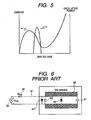
- the element oscillates as the voltage is biased near the negative resistance region of the voltage/current (V-I) characteristic as illustrated in FIG. 5 .
- V-I voltage/current
- a power bias circuit is formed by 65, 66 and 67.
- the negative resistance is cancelled in a low frequency region so as not to generate any gain and suppress any parasitic oscillation by replacing diode element 63 with a resistance element whose resistance is substantially same as the negative resistance of the RTD element 64 of FIG. 6 .
- the low frequency as used herein is substantially of the order of kHz and MHz, although it may vary depending on the length of the cable for connecting the power bias circuit to the RTD element.
- the resistance value of a resistance element as described above is about tens of several ohms ( ⁇ ) and a DC current that does not participate in oscillation flows to the resistance element to provide a limit to improvement of power conversion efficiency.
- NPL 1 employs a diode element 63 to replace a resistance element as described above. Any parasitic oscillation is prevented from appearing by selecting a differential resistance value that can cancel the negative resistance for the diode element 63 near the bias voltage when the RTD element is driven to oscillate. With such an arrangement again, a DC current is made to flow to an element other than the RTD element to provide a limit to reduction of power consumption.
- both a resistance element and a diode element emit heat to consume electric power as an electric current is made to flow to them. Then, as a result, the RTD element is heated as heat emitting members are integrally arranged near the RTD element to reduce the service life and the gain of the element.
- an oscillator according to the present invention may have a more specific configuration as described bellow.
- part of the resonator operates as two electrodes of the negative resistance element and the capacitor is electrically connected in parallel with the electrodes.
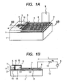
- Embodiment 1 of the present invention has a structure formed by integrating an RTD element and a large capacitance capacitor on a same substrate.
- FIGS. 1A and 1B illustrate the structure thereof, of which FIG. 1A is a schematic perspective view and FIG. 1B is a schematic cross-sectional view taken along 1B-1B in FIG. 1A .
- 4 denotes a post-shaped RTD element and the structure further includes epitaxial layers including an InGaAs/AlAs or InGaAs/InAlAs quantum well 17, a pair of contact layers 15, 16 and spacer layers (not illustrated) formed on an InP substrate 1 by crystal growth thereof.
- a negative resistance element formed by using a III-V group compound semiconductor such as AlGaAs/GaAs on a GaAs substrate and AlGaN/InGaN on a GaN substrate, a IV group semiconductor such as Si/SiGe on an Si substrate, and a II-VI group semiconductor may also be applicable.
- the resonator is formed by an electrode 2 that also operates as a ground plane, an electrode 5 that also operates as a patch antenna and a power supply, and a dielectric 3 sandwiched between them.
- a dielectric 3 showing only little loss in the region of oscillation thereof is preferable.
- Preferable exemplar dielectrics include BCB (tradename: Benzocyclobutene), polyimide, polyethylene and polyolefin and BCB is employed here.
- one of the contacts of the RTD element 4 is connected to the ground plane electrode 2 by way of n+InGaAs contact layer 15, while the other contact is connected to the electrode 5 that is turned to a patch antenna by way of n+InGaAs contact layer 16.
- the antenna 5 is electrically connected to a line 10 and electrodes 6 and 7 that form a capacitance element so that power can be bias-supplied to the RTD element 4 by way of a cable line 13 and the electrodes 2 and 7 from electrical power supply 9.
- the oscillator is designed with the effective length for which the wavelength reducing effect is taken into consideration because of the presence of a dielectric so that the distance is about a half of the distance in a free space although the distance may depend on the material that is employed. This is due to the fact that the length that is generally referred to as intra-tube wavelength or electrical length is reduced by about 1/ ⁇ eff , where ⁇ eff is the effective dielectric constant. Then, the capacitor that operates as the first capacitor shares the dielectric 3 for forming the patch antenna 5. Due to the provision of the first capacitor, it is possible to oscillate only at a desired oscillation frequency, preventing the parasitic oscillation attributable to the line necessary for supplying a bias to a certain extent.
- the electrode 6 may have sides that are about several times of 100 ⁇ m long.
- a second capacitor C 2 (12) of a relatively large capacitance (of a magnitude of the order between nF and ⁇ F) is connected in parallel with the first capacitor close to the bias circuit of the first capacitor.
- a material 8 having a large dielectric constant is selected, and then made to show a small thickness.
- the second capacitor 12 can be made to show a capacitance of about 100 nF by using a high dielectric constant material (e.g., titanium oxide and barium titanate), for example a specific dielectric constant of not less than several times of 10, a thickness of about 0.1 ⁇ m and an area of 1 cm 2 (with 1 cm sides).
- the plurality of capacitors is integrated on a same substrate. While both of the electrodes 6 and 7 are drawn to show a same width in FIGS. 1A and 1B , they may produce a step not only in the direction of height but also in the width direction as long as the electrodes 6 and 7 are electrically connected each other.
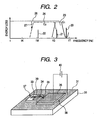
- FIG. 2 illustrates frequency bands.
- the horizontal axis is a logarithmic axis that shows steps of 1,000 Hz for frequencies starting from 1 Hz up to 1 THz.
- the vertical axis schematically shows the energy loss quantities at the oscillation circuit and at the power bias circuit with an arbitrarily selected scale.
- the trapezoidal graph 23 drawn by a solid line shows the characteristic determined by the first capacitor C 1 to prove that the loss is small at the desired oscillation frequency as indicated by a thick solid line 20 (e.g., 700 GHz) but increases at frequencies below the desired frequency.
- a filter element is formed with a cut-off frequency f that is defined by the formula (1) shown below, where Rs is the resistance (14) that is the sum of the internal resistance of the bias circuit and the resistance of the cable line 13 and C 1 is the capacitance of the capacitor.
- f 1 / C 1 ⁇ Rs ⁇ 2 ⁇ ⁇
- the cut-off frequency that is formed with a capacitor C 1 having a capacitance of 1 pF and resistor Rs having a resistance of 10 ⁇ is about 16 GHz.
- the loss is increased by a resistance element or a diode element because of the parasitic oscillation that arises at below the cut-off frequency.
- This is the characteristic indicated by the dotted line 26 in FIG. 2 and a window region that is free from loss at the point of oscillation 20 is formed by arranging such an element at a position separated from the RTD element by ⁇ /4 for oscillations.
- the parasitic oscillation in a lower frequency region is suppressed by utilizing the trapezoidal characteristic graph of a chain line 24 produced by the second capacitor 12 without using a resistance element.
- the cut-off frequency 27 is about 1.60 MHz as it is determined by the above formula (1) (as for the part of C 1 , C 1 + C 2 ⁇ C 2 ) so that the frequency can be made lower than the point of oscillation 22 of the power bias circuit.
- the frequency of the oscillation attributable to the power bias circuit is determined by the condition of oscillation of the two terminal loop feedback circuit using the RTD element 4 as gain element.
- the resonance frequency 22 of the power bias circuit is expressed by the formula (2) shown below.
- the resonance frequency is about 150 MHz. Then, as a result, any parasitic oscillation attributable to the bias circuit can be suppressed by the second capacitor 12.
- the cut-off effect of the second capacitor for a higher frequency band is determined by the dielectric for forming the capacitance element in the case of a MIM (metal-insulator-metal) structure and the use of a dielectric material whose dielectric constant does not significantly change up to about several times of 10 GHz may be satisfactory.
- MIM metal-insulator-metal
- a resonance point 21 can take place due to reflection or the like depending on the discontinuous quantity of the first capacitor and the second capacitor, it is desirably found in the suppressible frequency band of the first capacitor. From the description given above by referring to FIG. 2 , it will be clear that a resonator according to the present invention needs to be designed so as to establish a proper relationship for the total series resistance Rs of the bias circuit, the frequency of the oscillation attributable to the bias circuit and the cut-off frequency produced by the first and the second capacitors. In other words, with such an arrangement, any parasitic oscillation can be suppressed without using a resistance element and the ineffective DC current that does not participate in oscillation can be minimized.
- the design of the RTD element becomes subject to changes depending of the cable resistance of the power bias circuit, the internal resistance of the power source and the cable length, and there is a restriction that no biasing is possible in the negative resistance region unless the total resistance value is smaller than the absolute value of the negative resistance of the RTD element 4.
- the total series resistance Rs attributable to the power bias circuit determines the inclination -1/Rs of the load line for driving the element.
- Rs is greater than the negative resistance, or -1/Rs > -1/Rrtd
- the load line intersects the I-V curve of the RTD before and after the negative resistance region so that a skip takes place to either of the stable points for biasing (see, for example NPL 2).
- a capacitor is arranged to replace a resistance element etc. Then, the capacitance of the capacitor is so determined as to provide a cut-off frequency (inversely proportional to the product of multiplication of the capacitance by the resistance) that is smaller than the resonance frequency (e.g., 150 MHz) that is determined by the length of the power bias circuit and other factors. This is because the length of the arrangement other than the power bias circuit is shorter and hence the cut-off frequency will be greater than the resonance frequency.
- the capacitance is proportional to the dielectric constant and the area and inversely proportional to the distance between the electrodes.
- the dielectric that is selected to form the oscillation circuit including the RTD element should show little loss for the electromagnetic wave produced by oscillation of the oscillation circuit and the structure of the oscillation circuit needs to be so determined as to realize impedance matching with air. While the area needs to be large in order to provide a large capacitance, a too large area is not desirable because the components such as the resistance other than the capacitance increase accordingly and the desired high frequency characteristic may not be obtained when the area is increased. For this reason, a first capacitor having the above-described capacitance and a second capacitor having a different capacitance are provided.
- any electromagnetic wave showing a resonance frequency that is determined by the discontinuous quantity of impedance and the electrical length between the first capacitor and the second capacitor needs to be cut out by the first capacitor because the second capacitor cannot suppress oscillation if it is not cut out by the first capacitor. Since the resonance frequency becomes small when the electrical length between the first capacitor and the second capacitor increases (see the formula (2) above), the electrical length should be such that the first capacitor can cut out the electromagnetic wave of the resonance frequency.
- an,oscillator showing high power conversion efficiency and emitting little heat can be provided by using capacitors to suppress the parasitic oscillation attributable to the power bias circuit and so on. Then, as a result, it is possible to realize an oscillator having a structure that can reduce the power consumption, improve the service life and prevent any decrease of gain. Additionally, a very compact terahertz imaging apparatus and terahertz analyzing device showing a very low power consumption rate can be realized by using such an oscillator.
- a spacer layer made of non-doped InGaAs, an n-type InGaAs electric contact layer and an n+InGaAs contact layer are arranged at the top and also at the bottom of the triple barrier quantum well structure.
- the electrode 5 of the patch antenna has a square pattern of 150 ⁇ m ⁇ 150 ⁇ m and the post is located at a position moved for 40 ⁇ m from the center thereof in parallel in the direction of moving away from the electrode 6.
- the resonator is prepared so as to make the patch antenna resonator and the RTD element show impedance matching. Since the antenna size approximately corresponds to ⁇ /2, the oscillation frequency is about 530 GHz.
- the electrodes 2 and 5 are made of Ti/Pd/Au (20 nm/20 nm/200 nm).
- the line 10 has a width of 12 ⁇ m and a length of 75 ⁇ m and is designed to be a ⁇ /4 line relative to the oscillation wavelength of 530 GHz.
- the electrode 6 for forming the first capacitor is made to show a rectangular profile of 200 ⁇ m ⁇ 1,000 ⁇ m so as to have a capacitance of several pF.
- the dielectric 8 is made of titanium oxide (0.1 ⁇ m thick) showing a dielectric constant of about 30 and the electrode 7 is made to show a profile of 1,000 ⁇ m ⁇ 1,000 ⁇ m so as to have a capacitance of about 2 nF.
- the cut-off frequency is about 8 MHz when connected to a power bias circuit of 10 ⁇ so that oscillation is obtained with a fundamental wave of 530 GHz without giving rise to any parasitic oscillation if the cable is shorter than about 18 m.
- Embodiment 2 of the present invention has such a structure that a second capacitor is installed on a same mount as a separate chip as illustrated in FIG. 3 .
- 30 denotes a sub-carrier for installing the chips.
- a substrate prepared by coating an electroconductive layer 31 such as Au on a ceramic substrate such as Si substrate, Al 2 O 3 and AlN or on a plastic substrate or a metal plate may selectively be employed for the sub-carrier 30.
- 37 denotes an RTD element chip or a single chip realized to carry the RTD element and components down to the part that corresponds to the first capacitor of Embodiment 1.
- a patch antenna 33 and an electrode 34 are connected by a line 39.
- the capacitance of the part that corresponds to the first capacitor needs to be made larger than that of Embodiment 1.
- One of the contacts of the RTD element is connected to the electroconductive layer 31 of the sub-carrier and the other contact is connected to one of the electrodes (36) of chip capacitor 38 that forms a second capacitor by means of Au wire bonding 35. While there is a single wire bonding 35 in FIG. 3 , a plurality of wire bondings may be provided if necessary.
- the other electrode of the chip capacitor 38 is electroconductively connected to the electroconductive layer 31 of the sub-carrier. Resonance point 21 in the frequency band of FIG.
- Power bias circuit 40 is connected to the electrode 36 of the chip capacitor and the electroconductive layer 31 of the sub-carrier.
- This embodiment provides a higher degree of freedom and a relatively large capacitor such as 1 ⁇ F can be connected because separate capacitors can be selected and installed in this embodiment.
- a high degree of freedom can increase for the cable length and the resistance of the power bias circuit to be used because the lower cut-off frequency falls when the capacitance increases.
- the cut-off frequency is about 16 kHz, therefore Embodiment 2 provides an effect of suppressing any parasitic oscillation so long as the cable length is of the order of km.
- While the second capacitor is a chip capacitor, components down to the second capacitor may be integrated with the RTD element and the third capacitor and the subsequent components may be realized as a separate chip by taking the parasitic inductance due to individual capacitors into consideration.
- a resonator disclosed in Embodiment 3 of the present invention has a stripe-shaped resonator formed by an RTD element as illustrated in FIG. 4 .
- the crystal structure of the RTD element has structure such as the semiconductor described in Example of Embodiment 1, for example, a layer 46 including an InGaAs/AlAs multiple quantum well formed by epitaxial growth on an InP substrate and n+InGaAs 47, 48 that operate as contact layer.
- a dielectric waveguide in the terahertz band and a double plasmon waveguide formed by sandwiching a substrate between metal plates is preferably employed. For this reason, the substrate 49 illustrated in FIG.
- GaAs or InP is suitably employed as a material having an expansion coefficient close to that of an epitaxial thin film.
- An Si substrate or a ceramic substrate may also be used.
- a metal film 43, Ti/Au thin film for example, is formed on the surface of the substrate 49 and bonded to an epitaxially grown film by Au-Au metal bonding (not illustrated), and the InP substrate that is used at the time of growing the epitaxially grown film is removed by etching.
- reference sign 45 denotes a dielectric section formed by BCB resin around the epitaxial layer and a first capacitor is formed by the dielectric section 45, an upper electrode 41 and a lower electrode 43.
- the layer 46 including the multiple quantum well has a width of 20 ⁇ m and the assemble including the dielectric section 45 is 300 ⁇ m wide, while the strip has a length of 500 ⁇ m, although the dimensions may be selected depending on the epitaxial structure and the designed oscillation frequency.
- a dielectric 42 having a high dielectric constant and a thin thickness (e.g., 0.1 ⁇ m thick titanium oxide thin film) unlike the dielectric section 45 is formed around the stripe-shaped region and a second capacitor is formed by the electrode 41 extended from the stripe-shaped section and the electrode 43.
- power bias circuit 50 is connected to the electrode 41 and the electrode 43.
- This invention relates to an oscillator having a negative resistance element for generating an electromagnetic wave (a terahertz wave in particular).
- an oscillator can find applications in tomography apparatus, spectrometric examination apparatus and radio communication equipment to operate as light source section.
Landscapes
- Inductance-Capacitance Distribution Constants And Capacitance-Resistance Oscillators (AREA)
- Control Of Motors That Do Not Use Commutators (AREA)
Applications Claiming Priority (2)
| Application Number | Priority Date | Filing Date | Title |
|---|---|---|---|
| JP2009205673A JP5612842B2 (ja) | 2009-09-07 | 2009-09-07 | 発振器 |
| PCT/JP2010/064036 WO2011027671A1 (en) | 2009-09-07 | 2010-08-13 | Oscillator having negative resistance element |
Publications (2)
| Publication Number | Publication Date |
|---|---|
| EP2476205A1 EP2476205A1 (en) | 2012-07-18 |
| EP2476205B1 true EP2476205B1 (en) | 2014-07-16 |
Family
ID=43003801
Family Applications (1)
| Application Number | Title | Priority Date | Filing Date |
|---|---|---|---|
| EP10749690.3A Not-in-force EP2476205B1 (en) | 2009-09-07 | 2010-08-13 | Oscillator having negative resistance element |
Country Status (8)
| Country | Link |
|---|---|
| US (1) | US8779864B2 (enExample) |
| EP (1) | EP2476205B1 (enExample) |
| JP (1) | JP5612842B2 (enExample) |
| KR (1) | KR101357660B1 (enExample) |
| CN (1) | CN102484450B (enExample) |
| BR (1) | BR112012005049A2 (enExample) |
| RU (1) | RU2486660C1 (enExample) |
| WO (1) | WO2011027671A1 (enExample) |
Families Citing this family (17)
| Publication number | Priority date | Publication date | Assignee | Title |
|---|---|---|---|---|
| JP5808560B2 (ja) * | 2011-04-01 | 2015-11-10 | ローム株式会社 | テラヘルツ発振検出素子 |
| JP2013236326A (ja) * | 2012-05-10 | 2013-11-21 | Canon Inc | 発振素子、受信素子、及び測定装置 |
| JP6280310B2 (ja) * | 2012-06-06 | 2018-02-14 | キヤノン株式会社 | 発振器 |
| JP2014127715A (ja) * | 2012-12-27 | 2014-07-07 | Toshiba Corp | 半導体装置 |
| JP6100024B2 (ja) * | 2013-02-27 | 2017-03-22 | キヤノン株式会社 | 発振素子 |
| JP6373010B2 (ja) * | 2013-03-12 | 2018-08-15 | キヤノン株式会社 | 発振素子 |
| JP2014207654A (ja) * | 2013-03-16 | 2014-10-30 | キヤノン株式会社 | 導波路素子 |
| CN103762416B (zh) * | 2014-02-25 | 2016-12-07 | 中国工程物理研究院电子工程研究所 | 一种太赫兹波片载-波导-喇叭转换天线 |
| JP6794508B2 (ja) * | 2014-02-28 | 2020-12-02 | キヤノン株式会社 | 発振素子、及びこれを用いた発振器 |
| JP6562645B2 (ja) * | 2014-02-28 | 2019-08-21 | キヤノン株式会社 | 発振素子、及びこれを用いた発振器 |
| JP6870135B2 (ja) * | 2014-02-28 | 2021-05-12 | キヤノン株式会社 | 素子 |
| JP6682185B2 (ja) * | 2014-02-28 | 2020-04-15 | キヤノン株式会社 | 素子 |
| JP2016036128A (ja) * | 2014-07-31 | 2016-03-17 | キヤノン株式会社 | 発振素子 |
| US9899959B2 (en) * | 2015-05-22 | 2018-02-20 | Canon Kabushiki Kaisha | Element, and oscillator and information acquiring device including the element |
| US9866245B2 (en) | 2015-11-18 | 2018-01-09 | Linear Technology Corporation | Active differential resistors with reduced noise |
| JP7516009B2 (ja) | 2019-02-20 | 2024-07-16 | キヤノン株式会社 | 発振器、撮像装置 |
| JP7493922B2 (ja) | 2019-08-26 | 2024-06-03 | キヤノン株式会社 | 発振器、撮像装置 |
Family Cites Families (41)
| Publication number | Priority date | Publication date | Assignee | Title |
|---|---|---|---|---|
| JP2800566B2 (ja) * | 1991-07-23 | 1998-09-21 | 日本電気株式会社 | 電界効果トランジスタおよび高周波信号発振器および周波数変換回路 |
| JP3210159B2 (ja) | 1993-12-10 | 2001-09-17 | キヤノン株式会社 | 半導体レーザ、光源装置、光通信システム及び光通信方法 |
| JPH07307530A (ja) | 1994-03-17 | 1995-11-21 | Canon Inc | 偏波変調可能な半導体レーザ |
| US5659560A (en) | 1994-05-12 | 1997-08-19 | Canon Kabushiki Kaisha | Apparatus and method for driving oscillation polarization selective light source, and optical communication system using the same |
| US5539761A (en) * | 1994-05-24 | 1996-07-23 | Yissum Research Development Company Of The Hebrew University Of Jerusalem | Resonant tunneling oscillators |
| US5764670A (en) | 1995-02-27 | 1998-06-09 | Canon Kabushiki Kaisha | Semiconductor laser apparatus requiring no external modulator, method of driving semiconductor laser device, and optical communication system using the semiconductor laser apparatus |
| JP2001042170A (ja) | 1999-07-28 | 2001-02-16 | Canon Inc | 光配線装置、その駆動方法およびそれを用いた電子機器 |
| RU2190921C2 (ru) * | 1999-12-31 | 2002-10-10 | Таганрогский государственный радиотехнический университет | Генератор сверхвысоких частот |
| JP4588947B2 (ja) * | 2001-12-28 | 2010-12-01 | 日本電波工業株式会社 | コプレーナライン型の高周波発振器 |
| US7630588B2 (en) | 2003-06-25 | 2009-12-08 | Canon Kabushiki Kaisha | High frequency electrical signal control device and sensing system |
| JP4136858B2 (ja) | 2003-09-12 | 2008-08-20 | キヤノン株式会社 | 位置検出装置、及び情報入力装置 |
| JP2005157601A (ja) | 2003-11-25 | 2005-06-16 | Canon Inc | 電磁波による積層状物体計数装置及び計数方法 |
| RU37896U1 (ru) * | 2003-12-05 | 2004-05-10 | Бокова Оксана Игоревна | Автогенератор на туннельном диоде |
| JP4217646B2 (ja) | 2004-03-26 | 2009-02-04 | キヤノン株式会社 | 認証方法及び認証装置 |
| JP4250573B2 (ja) | 2004-07-16 | 2009-04-08 | キヤノン株式会社 | 素子 |
| JP4546326B2 (ja) | 2004-07-30 | 2010-09-15 | キヤノン株式会社 | センシング装置 |
| JP4390147B2 (ja) | 2005-03-28 | 2009-12-24 | キヤノン株式会社 | 周波数可変発振器 |
| JP4250603B2 (ja) | 2005-03-28 | 2009-04-08 | キヤノン株式会社 | テラヘルツ波の発生素子、及びその製造方法 |
| JP2006275910A (ja) | 2005-03-30 | 2006-10-12 | Canon Inc | 位置センシング装置及び位置センシング方法 |
| JP4402026B2 (ja) | 2005-08-30 | 2010-01-20 | キヤノン株式会社 | センシング装置 |
| JP2007124250A (ja) | 2005-10-27 | 2007-05-17 | Tokyo Institute Of Technology | テラヘルツ発振素子 |
| JP4773839B2 (ja) | 2006-02-15 | 2011-09-14 | キヤノン株式会社 | 対象物の情報を検出する検出装置 |
| JP5132146B2 (ja) | 2006-03-17 | 2013-01-30 | キヤノン株式会社 | 分析方法、分析装置、及び検体保持部材 |
| JP4481946B2 (ja) | 2006-03-17 | 2010-06-16 | キヤノン株式会社 | 検出素子及び画像形成装置 |
| JP4898472B2 (ja) | 2006-04-11 | 2012-03-14 | キヤノン株式会社 | 検査装置 |
| JP4709059B2 (ja) | 2006-04-28 | 2011-06-22 | キヤノン株式会社 | 検査装置及び検査方法 |
| JP5028068B2 (ja) * | 2006-05-31 | 2012-09-19 | キヤノン株式会社 | アクティブアンテナ発振器 |
| JP5196750B2 (ja) | 2006-08-25 | 2013-05-15 | キヤノン株式会社 | 発振素子 |
| JP4873746B2 (ja) | 2006-12-21 | 2012-02-08 | キヤノン株式会社 | 発振素子 |
| RU2336625C1 (ru) * | 2007-05-24 | 2008-10-20 | Андрей Борисович Козырев | Свч-автогенератор |
| JP5144175B2 (ja) | 2007-08-31 | 2013-02-13 | キヤノン株式会社 | 電磁波を用いる検査装置及び検査方法 |
| US7869036B2 (en) | 2007-08-31 | 2011-01-11 | Canon Kabushiki Kaisha | Analysis apparatus for analyzing a specimen by obtaining electromagnetic spectrum information |
| JP5171539B2 (ja) | 2007-11-29 | 2013-03-27 | キヤノン株式会社 | 共鳴トンネル構造体 |
| JP4807707B2 (ja) | 2007-11-30 | 2011-11-02 | キヤノン株式会社 | 波形情報取得装置 |
| JP4834718B2 (ja) | 2008-01-29 | 2011-12-14 | キヤノン株式会社 | パルスレーザ装置、テラヘルツ発生装置、テラヘルツ計測装置及びテラヘルツトモグラフィー装置 |
| JP5357531B2 (ja) | 2008-02-05 | 2013-12-04 | キヤノン株式会社 | 情報取得装置及び情報取得方法 |
| JP5506258B2 (ja) | 2008-08-06 | 2014-05-28 | キヤノン株式会社 | 整流素子 |
| JP5665305B2 (ja) | 2008-12-25 | 2015-02-04 | キヤノン株式会社 | 分析装置 |
| TW201027512A (en) | 2009-01-06 | 2010-07-16 | Novatek Microelectronics Corp | Data driving circuit for flat display panel with partial mode and method for processing pixel data of a partial window |
| JP5717336B2 (ja) | 2009-03-27 | 2015-05-13 | キヤノン株式会社 | 発振器 |
| JP5563356B2 (ja) | 2010-04-12 | 2014-07-30 | キヤノン株式会社 | 電磁波検出素子 |
-
2009
- 2009-09-07 JP JP2009205673A patent/JP5612842B2/ja active Active
-
2010
- 2010-08-13 RU RU2012113540/08A patent/RU2486660C1/ru not_active IP Right Cessation
- 2010-08-13 EP EP10749690.3A patent/EP2476205B1/en not_active Not-in-force
- 2010-08-13 US US13/384,223 patent/US8779864B2/en active Active
- 2010-08-13 BR BR112012005049A patent/BR112012005049A2/pt not_active Application Discontinuation
- 2010-08-13 KR KR1020127008595A patent/KR101357660B1/ko not_active Expired - Fee Related
- 2010-08-13 WO PCT/JP2010/064036 patent/WO2011027671A1/en not_active Ceased
- 2010-08-13 CN CN201080039684.6A patent/CN102484450B/zh active Active
Also Published As
| Publication number | Publication date |
|---|---|
| JP2011061276A (ja) | 2011-03-24 |
| US20120105161A1 (en) | 2012-05-03 |
| EP2476205A1 (en) | 2012-07-18 |
| JP5612842B2 (ja) | 2014-10-22 |
| KR101357660B1 (ko) | 2014-02-05 |
| CN102484450B (zh) | 2014-11-12 |
| US8779864B2 (en) | 2014-07-15 |
| WO2011027671A1 (en) | 2011-03-10 |
| RU2486660C1 (ru) | 2013-06-27 |
| CN102484450A (zh) | 2012-05-30 |
| BR112012005049A2 (pt) | 2017-01-31 |
| KR20120062867A (ko) | 2012-06-14 |
Similar Documents
| Publication | Publication Date | Title |
|---|---|---|
| EP2476205B1 (en) | Oscillator having negative resistance element | |
| US11309834B2 (en) | High-power terahertz oscillator | |
| EP2412092B1 (en) | Oscillator | |
| US9236833B2 (en) | Electromagnetic wave generation device and detection device | |
| JP5127360B2 (ja) | 発振素子、及び検査装置 | |
| US7570216B2 (en) | Antenna device | |
| US9819145B2 (en) | Laser and integrated graphene modulator | |
| JP2008053519A (ja) | 発振素子 | |
| JP2021153185A (ja) | 半導体素子 | |
| JP5808560B2 (ja) | テラヘルツ発振検出素子 | |
| US20160373061A1 (en) | Oscillation element and oscillator using the same | |
| US9899959B2 (en) | Element, and oscillator and information acquiring device including the element | |
| CN108566164B (zh) | 一种基于共振遂穿二极管的太赫兹振荡电路及振荡器 | |
| US9438168B2 (en) | Oscillator | |
| Ouřednik | Advanced concepts of THz resonant-tunnelling-diode oscillators | |
| Jagtap et al. | Internally Integrated Active-Type Patch Antenna for Semiconductor Superlattice THz Oscillators |
Legal Events
| Date | Code | Title | Description |
|---|---|---|---|
| PUAI | Public reference made under article 153(3) epc to a published international application that has entered the european phase |
Free format text: ORIGINAL CODE: 0009012 |
|
| 17P | Request for examination filed |
Effective date: 20120410 |
|
| AK | Designated contracting states |
Kind code of ref document: A1 Designated state(s): AL AT BE BG CH CY CZ DE DK EE ES FI FR GB GR HR HU IE IS IT LI LT LU LV MC MK MT NL NO PL PT RO SE SI SK SM TR |
|
| DAX | Request for extension of the european patent (deleted) | ||
| GRAP | Despatch of communication of intention to grant a patent |
Free format text: ORIGINAL CODE: EPIDOSNIGR1 |
|
| INTG | Intention to grant announced |
Effective date: 20130927 |
|
| GRAP | Despatch of communication of intention to grant a patent |
Free format text: ORIGINAL CODE: EPIDOSNIGR1 |
|
| INTG | Intention to grant announced |
Effective date: 20140206 |
|
| GRAS | Grant fee paid |
Free format text: ORIGINAL CODE: EPIDOSNIGR3 |
|
| GRAA | (expected) grant |
Free format text: ORIGINAL CODE: 0009210 |
|
| AK | Designated contracting states |
Kind code of ref document: B1 Designated state(s): AL AT BE BG CH CY CZ DE DK EE ES FI FR GB GR HR HU IE IS IT LI LT LU LV MC MK MT NL NO PL PT RO SE SI SK SM TR |
|
| REG | Reference to a national code |
Ref country code: GB Ref legal event code: FG4D |
|
| REG | Reference to a national code |
Ref country code: CH Ref legal event code: EP |
|
| REG | Reference to a national code |
Ref country code: IE Ref legal event code: FG4D |
|
| REG | Reference to a national code |
Ref country code: AT Ref legal event code: REF Ref document number: 678163 Country of ref document: AT Kind code of ref document: T Effective date: 20140815 |
|
| REG | Reference to a national code |
Ref country code: DE Ref legal event code: R096 Ref document number: 602010017535 Country of ref document: DE Effective date: 20140828 |
|
| REG | Reference to a national code |
Ref country code: NL Ref legal event code: VDEP Effective date: 20140716 |
|
| REG | Reference to a national code |
Ref country code: AT Ref legal event code: MK05 Ref document number: 678163 Country of ref document: AT Kind code of ref document: T Effective date: 20140716 |
|
| REG | Reference to a national code |
Ref country code: LT Ref legal event code: MG4D |
|
| PG25 | Lapsed in a contracting state [announced via postgrant information from national office to epo] |
Ref country code: FI Free format text: LAPSE BECAUSE OF FAILURE TO SUBMIT A TRANSLATION OF THE DESCRIPTION OR TO PAY THE FEE WITHIN THE PRESCRIBED TIME-LIMIT Effective date: 20140716 Ref country code: BG Free format text: LAPSE BECAUSE OF FAILURE TO SUBMIT A TRANSLATION OF THE DESCRIPTION OR TO PAY THE FEE WITHIN THE PRESCRIBED TIME-LIMIT Effective date: 20141016 Ref country code: LT Free format text: LAPSE BECAUSE OF FAILURE TO SUBMIT A TRANSLATION OF THE DESCRIPTION OR TO PAY THE FEE WITHIN THE PRESCRIBED TIME-LIMIT Effective date: 20140716 Ref country code: PT Free format text: LAPSE BECAUSE OF FAILURE TO SUBMIT A TRANSLATION OF THE DESCRIPTION OR TO PAY THE FEE WITHIN THE PRESCRIBED TIME-LIMIT Effective date: 20141117 Ref country code: ES Free format text: LAPSE BECAUSE OF FAILURE TO SUBMIT A TRANSLATION OF THE DESCRIPTION OR TO PAY THE FEE WITHIN THE PRESCRIBED TIME-LIMIT Effective date: 20140716 Ref country code: NO Free format text: LAPSE BECAUSE OF FAILURE TO SUBMIT A TRANSLATION OF THE DESCRIPTION OR TO PAY THE FEE WITHIN THE PRESCRIBED TIME-LIMIT Effective date: 20141016 Ref country code: SE Free format text: LAPSE BECAUSE OF FAILURE TO SUBMIT A TRANSLATION OF THE DESCRIPTION OR TO PAY THE FEE WITHIN THE PRESCRIBED TIME-LIMIT Effective date: 20140716 Ref country code: GR Free format text: LAPSE BECAUSE OF FAILURE TO SUBMIT A TRANSLATION OF THE DESCRIPTION OR TO PAY THE FEE WITHIN THE PRESCRIBED TIME-LIMIT Effective date: 20141017 |
|
| PG25 | Lapsed in a contracting state [announced via postgrant information from national office to epo] |
Ref country code: CY Free format text: LAPSE BECAUSE OF FAILURE TO SUBMIT A TRANSLATION OF THE DESCRIPTION OR TO PAY THE FEE WITHIN THE PRESCRIBED TIME-LIMIT Effective date: 20140716 Ref country code: NL Free format text: LAPSE BECAUSE OF FAILURE TO SUBMIT A TRANSLATION OF THE DESCRIPTION OR TO PAY THE FEE WITHIN THE PRESCRIBED TIME-LIMIT Effective date: 20140716 Ref country code: PL Free format text: LAPSE BECAUSE OF FAILURE TO SUBMIT A TRANSLATION OF THE DESCRIPTION OR TO PAY THE FEE WITHIN THE PRESCRIBED TIME-LIMIT Effective date: 20140716 Ref country code: IS Free format text: LAPSE BECAUSE OF FAILURE TO SUBMIT A TRANSLATION OF THE DESCRIPTION OR TO PAY THE FEE WITHIN THE PRESCRIBED TIME-LIMIT Effective date: 20141116 Ref country code: AT Free format text: LAPSE BECAUSE OF FAILURE TO SUBMIT A TRANSLATION OF THE DESCRIPTION OR TO PAY THE FEE WITHIN THE PRESCRIBED TIME-LIMIT Effective date: 20140716 Ref country code: LV Free format text: LAPSE BECAUSE OF FAILURE TO SUBMIT A TRANSLATION OF THE DESCRIPTION OR TO PAY THE FEE WITHIN THE PRESCRIBED TIME-LIMIT Effective date: 20140716 |
|
| REG | Reference to a national code |
Ref country code: CH Ref legal event code: PL |
|
| REG | Reference to a national code |
Ref country code: DE Ref legal event code: R097 Ref document number: 602010017535 Country of ref document: DE |
|
| PG25 | Lapsed in a contracting state [announced via postgrant information from national office to epo] |
Ref country code: CZ Free format text: LAPSE BECAUSE OF FAILURE TO SUBMIT A TRANSLATION OF THE DESCRIPTION OR TO PAY THE FEE WITHIN THE PRESCRIBED TIME-LIMIT Effective date: 20140716 Ref country code: MC Free format text: LAPSE BECAUSE OF FAILURE TO SUBMIT A TRANSLATION OF THE DESCRIPTION OR TO PAY THE FEE WITHIN THE PRESCRIBED TIME-LIMIT Effective date: 20140716 Ref country code: SK Free format text: LAPSE BECAUSE OF FAILURE TO SUBMIT A TRANSLATION OF THE DESCRIPTION OR TO PAY THE FEE WITHIN THE PRESCRIBED TIME-LIMIT Effective date: 20140716 Ref country code: IT Free format text: LAPSE BECAUSE OF FAILURE TO SUBMIT A TRANSLATION OF THE DESCRIPTION OR TO PAY THE FEE WITHIN THE PRESCRIBED TIME-LIMIT Effective date: 20140716 Ref country code: DK Free format text: LAPSE BECAUSE OF FAILURE TO SUBMIT A TRANSLATION OF THE DESCRIPTION OR TO PAY THE FEE WITHIN THE PRESCRIBED TIME-LIMIT Effective date: 20140716 Ref country code: CH Free format text: LAPSE BECAUSE OF NON-PAYMENT OF DUE FEES Effective date: 20140831 Ref country code: BE Free format text: LAPSE BECAUSE OF NON-PAYMENT OF DUE FEES Effective date: 20140831 Ref country code: RO Free format text: LAPSE BECAUSE OF FAILURE TO SUBMIT A TRANSLATION OF THE DESCRIPTION OR TO PAY THE FEE WITHIN THE PRESCRIBED TIME-LIMIT Effective date: 20140716 Ref country code: EE Free format text: LAPSE BECAUSE OF FAILURE TO SUBMIT A TRANSLATION OF THE DESCRIPTION OR TO PAY THE FEE WITHIN THE PRESCRIBED TIME-LIMIT Effective date: 20140716 Ref country code: LI Free format text: LAPSE BECAUSE OF NON-PAYMENT OF DUE FEES Effective date: 20140831 |
|
| REG | Reference to a national code |
Ref country code: IE Ref legal event code: MM4A |
|
| PLBE | No opposition filed within time limit |
Free format text: ORIGINAL CODE: 0009261 |
|
| STAA | Information on the status of an ep patent application or granted ep patent |
Free format text: STATUS: NO OPPOSITION FILED WITHIN TIME LIMIT |
|
| REG | Reference to a national code |
Ref country code: FR Ref legal event code: ST Effective date: 20150430 |
|
| 26N | No opposition filed |
Effective date: 20150417 |
|
| PG25 | Lapsed in a contracting state [announced via postgrant information from national office to epo] |
Ref country code: IE Free format text: LAPSE BECAUSE OF NON-PAYMENT OF DUE FEES Effective date: 20140813 Ref country code: FR Free format text: LAPSE BECAUSE OF NON-PAYMENT OF DUE FEES Effective date: 20140916 |
|
| PG25 | Lapsed in a contracting state [announced via postgrant information from national office to epo] |
Ref country code: SI Free format text: LAPSE BECAUSE OF FAILURE TO SUBMIT A TRANSLATION OF THE DESCRIPTION OR TO PAY THE FEE WITHIN THE PRESCRIBED TIME-LIMIT Effective date: 20140716 |
|
| PG25 | Lapsed in a contracting state [announced via postgrant information from national office to epo] |
Ref country code: SM Free format text: LAPSE BECAUSE OF FAILURE TO SUBMIT A TRANSLATION OF THE DESCRIPTION OR TO PAY THE FEE WITHIN THE PRESCRIBED TIME-LIMIT Effective date: 20140716 |
|
| PG25 | Lapsed in a contracting state [announced via postgrant information from national office to epo] |
Ref country code: MT Free format text: LAPSE BECAUSE OF FAILURE TO SUBMIT A TRANSLATION OF THE DESCRIPTION OR TO PAY THE FEE WITHIN THE PRESCRIBED TIME-LIMIT Effective date: 20140716 |
|
| PG25 | Lapsed in a contracting state [announced via postgrant information from national office to epo] |
Ref country code: TR Free format text: LAPSE BECAUSE OF FAILURE TO SUBMIT A TRANSLATION OF THE DESCRIPTION OR TO PAY THE FEE WITHIN THE PRESCRIBED TIME-LIMIT Effective date: 20140716 Ref country code: HU Free format text: LAPSE BECAUSE OF FAILURE TO SUBMIT A TRANSLATION OF THE DESCRIPTION OR TO PAY THE FEE WITHIN THE PRESCRIBED TIME-LIMIT; INVALID AB INITIO Effective date: 20100813 Ref country code: LU Free format text: LAPSE BECAUSE OF NON-PAYMENT OF DUE FEES Effective date: 20140813 Ref country code: HR Free format text: LAPSE BECAUSE OF FAILURE TO SUBMIT A TRANSLATION OF THE DESCRIPTION OR TO PAY THE FEE WITHIN THE PRESCRIBED TIME-LIMIT Effective date: 20140716 Ref country code: BE Free format text: LAPSE BECAUSE OF FAILURE TO SUBMIT A TRANSLATION OF THE DESCRIPTION OR TO PAY THE FEE WITHIN THE PRESCRIBED TIME-LIMIT Effective date: 20140716 |
|
| PGFP | Annual fee paid to national office [announced via postgrant information from national office to epo] |
Ref country code: DE Payment date: 20160831 Year of fee payment: 7 Ref country code: GB Payment date: 20160825 Year of fee payment: 7 |
|
| REG | Reference to a national code |
Ref country code: DE Ref legal event code: R119 Ref document number: 602010017535 Country of ref document: DE |
|
| GBPC | Gb: european patent ceased through non-payment of renewal fee |
Effective date: 20170813 |
|
| PG25 | Lapsed in a contracting state [announced via postgrant information from national office to epo] |
Ref country code: MK Free format text: LAPSE BECAUSE OF FAILURE TO SUBMIT A TRANSLATION OF THE DESCRIPTION OR TO PAY THE FEE WITHIN THE PRESCRIBED TIME-LIMIT Effective date: 20140716 |
|
| PG25 | Lapsed in a contracting state [announced via postgrant information from national office to epo] |
Ref country code: GB Free format text: LAPSE BECAUSE OF NON-PAYMENT OF DUE FEES Effective date: 20170813 Ref country code: DE Free format text: LAPSE BECAUSE OF NON-PAYMENT OF DUE FEES Effective date: 20180301 |
|
| PG25 | Lapsed in a contracting state [announced via postgrant information from national office to epo] |
Ref country code: AL Free format text: LAPSE BECAUSE OF FAILURE TO SUBMIT A TRANSLATION OF THE DESCRIPTION OR TO PAY THE FEE WITHIN THE PRESCRIBED TIME-LIMIT Effective date: 20140716 |