JP2013236326A - 発振素子、受信素子、及び測定装置 - Google Patents
発振素子、受信素子、及び測定装置 Download PDFInfo
- Publication number
- JP2013236326A JP2013236326A JP2012108683A JP2012108683A JP2013236326A JP 2013236326 A JP2013236326 A JP 2013236326A JP 2012108683 A JP2012108683 A JP 2012108683A JP 2012108683 A JP2012108683 A JP 2012108683A JP 2013236326 A JP2013236326 A JP 2013236326A
- Authority
- JP
- Japan
- Prior art keywords
- conductor layer
- antenna
- oscillation element
- resonance
- conductor
- Prior art date
- Legal status (The legal status is an assumption and is not a legal conclusion. Google has not performed a legal analysis and makes no representation as to the accuracy of the status listed.)
- Pending
Links
- 230000010355 oscillation Effects 0.000 title claims abstract description 51
- 239000004020 conductor Substances 0.000 claims abstract description 134
- 239000010410 layer Substances 0.000 claims description 156
- 239000000758 substrate Substances 0.000 claims description 38
- 239000011229 interlayer Substances 0.000 claims description 12
- 230000007704 transition Effects 0.000 claims description 4
- 239000012212 insulator Substances 0.000 claims description 3
- 239000000969 carrier Substances 0.000 claims description 2
- 238000010030 laminating Methods 0.000 claims 1
- 238000000034 method Methods 0.000 abstract description 6
- 238000000605 extraction Methods 0.000 abstract description 2
- 238000003475 lamination Methods 0.000 abstract 2
- 239000010408 film Substances 0.000 description 18
- 239000004065 semiconductor Substances 0.000 description 15
- 229910000530 Gallium indium arsenide Inorganic materials 0.000 description 11
- 239000010931 gold Substances 0.000 description 10
- 239000000463 material Substances 0.000 description 9
- 238000004519 manufacturing process Methods 0.000 description 8
- XUIMIQQOPSSXEZ-UHFFFAOYSA-N Silicon Chemical compound [Si] XUIMIQQOPSSXEZ-UHFFFAOYSA-N 0.000 description 7
- 239000002184 metal Substances 0.000 description 7
- 229910052751 metal Inorganic materials 0.000 description 7
- 229910052710 silicon Inorganic materials 0.000 description 7
- 239000010703 silicon Substances 0.000 description 7
- UMIVXZPTRXBADB-UHFFFAOYSA-N benzocyclobutene Chemical compound C1=CC=C2CCC2=C1 UMIVXZPTRXBADB-UHFFFAOYSA-N 0.000 description 6
- 238000004364 calculation method Methods 0.000 description 5
- JBRZTFJDHDCESZ-UHFFFAOYSA-N AsGa Chemical compound [As]#[Ga] JBRZTFJDHDCESZ-UHFFFAOYSA-N 0.000 description 4
- 229910001218 Gallium arsenide Inorganic materials 0.000 description 4
- 230000004888 barrier function Effects 0.000 description 4
- 238000001312 dry etching Methods 0.000 description 4
- 238000007689 inspection Methods 0.000 description 3
- 239000011347 resin Substances 0.000 description 3
- 229920005989 resin Polymers 0.000 description 3
- VEXZGXHMUGYJMC-UHFFFAOYSA-N Hydrochloric acid Chemical compound Cl VEXZGXHMUGYJMC-UHFFFAOYSA-N 0.000 description 2
- 229910004298 SiO 2 Inorganic materials 0.000 description 2
- 239000000919 ceramic Substances 0.000 description 2
- 230000007423 decrease Effects 0.000 description 2
- 239000003814 drug Substances 0.000 description 2
- 230000005684 electric field Effects 0.000 description 2
- 238000005516 engineering process Methods 0.000 description 2
- 229910052737 gold Inorganic materials 0.000 description 2
- 229910010272 inorganic material Inorganic materials 0.000 description 2
- 239000011147 inorganic material Substances 0.000 description 2
- 239000011810 insulating material Substances 0.000 description 2
- 150000002739 metals Chemical class 0.000 description 2
- 238000000206 photolithography Methods 0.000 description 2
- 230000010287 polarization Effects 0.000 description 2
- 230000008569 process Effects 0.000 description 2
- 229910005540 GaP Inorganic materials 0.000 description 1
- 229910000673 Indium arsenide Inorganic materials 0.000 description 1
- 239000004642 Polyimide Substances 0.000 description 1
- 229910004541 SiN Inorganic materials 0.000 description 1
- 229910010413 TiO 2 Inorganic materials 0.000 description 1
- 238000010521 absorption reaction Methods 0.000 description 1
- 229910045601 alloy Inorganic materials 0.000 description 1
- 239000000956 alloy Substances 0.000 description 1
- 229910052782 aluminium Inorganic materials 0.000 description 1
- 229910052787 antimony Inorganic materials 0.000 description 1
- 239000012620 biological material Substances 0.000 description 1
- 230000015572 biosynthetic process Effects 0.000 description 1
- 229910052797 bismuth Inorganic materials 0.000 description 1
- 230000008859 change Effects 0.000 description 1
- 239000000470 constituent Substances 0.000 description 1
- 229910052802 copper Inorganic materials 0.000 description 1
- 239000012792 core layer Substances 0.000 description 1
- 238000013461 design Methods 0.000 description 1
- 239000003989 dielectric material Substances 0.000 description 1
- 239000012776 electronic material Substances 0.000 description 1
- 238000005530 etching Methods 0.000 description 1
- 238000001704 evaporation Methods 0.000 description 1
- 230000008020 evaporation Effects 0.000 description 1
- 239000000284 extract Substances 0.000 description 1
- 239000004744 fabric Substances 0.000 description 1
- HZXMRANICFIONG-UHFFFAOYSA-N gallium phosphide Chemical compound [Ga]#P HZXMRANICFIONG-UHFFFAOYSA-N 0.000 description 1
- 239000011521 glass Substances 0.000 description 1
- PCHJSUWPFVWCPO-UHFFFAOYSA-N gold Chemical compound [Au] PCHJSUWPFVWCPO-UHFFFAOYSA-N 0.000 description 1
- 238000003384 imaging method Methods 0.000 description 1
- RPQDHPTXJYYUPQ-UHFFFAOYSA-N indium arsenide Chemical compound [In]#[As] RPQDHPTXJYYUPQ-UHFFFAOYSA-N 0.000 description 1
- 238000002347 injection Methods 0.000 description 1
- 239000007924 injection Substances 0.000 description 1
- 239000012528 membrane Substances 0.000 description 1
- 229910052752 metalloid Inorganic materials 0.000 description 1
- 150000002738 metalloids Chemical class 0.000 description 1
- 230000003287 optical effect Effects 0.000 description 1
- 239000011368 organic material Substances 0.000 description 1
- 239000000123 paper Substances 0.000 description 1
- 229910021420 polycrystalline silicon Inorganic materials 0.000 description 1
- 229920001721 polyimide Polymers 0.000 description 1
- 229920005591 polysilicon Polymers 0.000 description 1
- 238000012545 processing Methods 0.000 description 1
- 238000012827 research and development Methods 0.000 description 1
- 229910052709 silver Inorganic materials 0.000 description 1
- 238000004528 spin coating Methods 0.000 description 1
- 239000010409 thin film Substances 0.000 description 1
- 230000009466 transformation Effects 0.000 description 1
- 230000005641 tunneling Effects 0.000 description 1
- 238000001771 vacuum deposition Methods 0.000 description 1
- 238000007740 vapor deposition Methods 0.000 description 1
Images


Classifications
-
- H—ELECTRICITY
- H01—ELECTRIC ELEMENTS
- H01Q—ANTENNAS, i.e. RADIO AERIALS
- H01Q1/00—Details of, or arrangements associated with, antennas
- H01Q1/50—Structural association of antennas with earthing switches, lead-in devices or lightning protectors
-
- G—PHYSICS
- G01—MEASURING; TESTING
- G01N—INVESTIGATING OR ANALYSING MATERIALS BY DETERMINING THEIR CHEMICAL OR PHYSICAL PROPERTIES
- G01N21/00—Investigating or analysing materials by the use of optical means, i.e. using sub-millimetre waves, infrared, visible or ultraviolet light
- G01N21/17—Systems in which incident light is modified in accordance with the properties of the material investigated
- G01N21/25—Colour; Spectral properties, i.e. comparison of effect of material on the light at two or more different wavelengths or wavelength bands
- G01N21/31—Investigating relative effect of material at wavelengths characteristic of specific elements or molecules, e.g. atomic absorption spectrometry
- G01N21/35—Investigating relative effect of material at wavelengths characteristic of specific elements or molecules, e.g. atomic absorption spectrometry using infrared light
- G01N21/3581—Investigating relative effect of material at wavelengths characteristic of specific elements or molecules, e.g. atomic absorption spectrometry using infrared light using far infrared light; using Terahertz radiation
-
- G—PHYSICS
- G01—MEASURING; TESTING
- G01N—INVESTIGATING OR ANALYSING MATERIALS BY DETERMINING THEIR CHEMICAL OR PHYSICAL PROPERTIES
- G01N22/00—Investigating or analysing materials by the use of microwaves or radio waves, i.e. electromagnetic waves with a wavelength of one millimetre or more
- G01N22/02—Investigating the presence of flaws
-
- H—ELECTRICITY
- H01—ELECTRIC ELEMENTS
- H01Q—ANTENNAS, i.e. RADIO AERIALS
- H01Q13/00—Waveguide horns or mouths; Slot antennas; Leaky-waveguide antennas; Equivalent structures causing radiation along the transmission path of a guided wave
-
- H—ELECTRICITY
- H04—ELECTRIC COMMUNICATION TECHNIQUE
- H04B—TRANSMISSION
- H04B1/00—Details of transmission systems, not covered by a single one of groups H04B3/00 - H04B13/00; Details of transmission systems not characterised by the medium used for transmission
- H04B1/06—Receivers
- H04B1/16—Circuits
Abstract
【解決手段】発振素子100は、電磁波を共振させるための共振部101と、共振部の端面に設けられて共振部から電磁波を出射させるための2つの導体層104、105を含む積層構造を有したアンテナ部102を備える。2つの導体層は、積層構造の積層方向に間隔を隔てて少なくとも一部が重なるインピーダンス整合に係る整合領域110を有する。整合領域は、共振部からアンテナ部に向かって伸長する方向に積層方向から見て先細りしたテーパー状を有する。
【選択図】図1
Description
(実施形態)
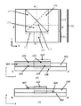
発振素子の一実施形態について、図1、図2及び図3を用いて説明する。図1は、発振素子100の外観を示す斜視図で、図2(a)は発振素子100の上面図、図2(b)、(c)はそれぞれ図2(a)のA−A’線、B−B’線における発振素子100の断面図である。また、図3は、複数の変形例のアンテナ部102の整合領域110の上面図である。
こうした受信素子は、電磁波を共振させるための共振部と、共振部の端面に設けられて共振部へと電磁波を入射させるための2つの導体層を含む積層構造を有したアンテナ部と、を備える。ここでも、整合領域は、共振部からアンテナ部に向かって伸長する方向に前記積層方向から見て先細りしたテーパー状を有する。
(実施例1)
本発明の発振素子の具体的な実施例1について、図5と図6を用いて説明する。図5は本実施例の斜視図で、図6は上面図である。本実施例では、活性層203として、サブバンド間遷移によりテラヘルツ波を発生するInGaAs/InAlAs系の3重障壁共鳴トンネルダイオード(RTD)構造を含む半導体積層構造を用いた。RTD構造は、n−InGaAs(厚さ50nm、Si、キャリア濃度2×1018cm−3)、InGaAs(5nm)、AlAs(1.3nm)、InGaAs(7.6nm)、InAlAs(2.6nm)、InGaAs(5.6nm)、AlAs(1.3nm)、InGaAs(5nm)、n−InGaAs(50nm、Si、2×1018cm−3)の順に積層された半導体量子井戸構造である。RTD構造の上下に配置された高濃度にキャリアドープしたn+InGaAs(400nm、1×1019cm−3)により、RTD構造と第一の導体層204及び第二の導体層205とを比較的低抵抗で接続する。
本発明の実施例2である発振素子300について、図7を用いて説明する。図7は素子の斜視図である。第一の基板303上に形成された共振部301は実施例1と同じRTD構造を用いている。また、その他の構成材料は基板を除き実施例1と同じものを用い、製造方法も共振部301の作製までは実施例1と同じ製造方法で作製した。ここで、基板は第一の基板303、第二の基板304ともに高抵抗シリコン基板を用いている。また、実施例1で述べたように、第一の基板303及び第二の基板304は、半導体、誘電体若しくは絶縁性材料であればシリコンに限らない。その後、層間絶縁膜305で活性層306の構造の埋め込みを行い、ドライエッチング法で活性層306の上部を露出させ、第二の導体層308を形成する。また、アンテナ部302の第三の導体層309と共振部の第一の導体層307は実施例1と同様に同時形成されている。アンテナ部302の第四の導体層310のパターンは第二の接合電極312も兼ねている。第四の導体層310形成と同時に第一の接合電極311も形成する。接合用金バンプ314を第一の接合電極311と第二の接合電極312上に形成し、第一の基板303と第二の基板304を対向させ、接合する。この様にして、アンテナ部は、第一の基板、2つの導体層の一方である第三の導体層、層間絶縁膜、2つの導体層の他方である第四の導体層、第二の基板の順に重なって構成される。
Claims (13)
- 電磁波を共振させるための共振部と、
前記共振部の端面に設けられて前記共振部から前記電磁波を出射させるための2つの導体層を含む積層構造を有したアンテナ部と、
を備えた電磁波を発振する発振素子であって、
前記2つの導体層は、前記積層構造の積層方向に間隔を隔てて少なくとも一部が重なるインピーダンス整合に係る整合領域を有し、
前記整合領域は、前記共振部から前記アンテナ部に向かって伸長する方向に前記積層方向から見て先細りしたテーパー状を有することを特徴とする発振素子。 - 前記共振部は、第一の導体層、電磁波に対して利得を有する利得媒質、第二の導体層がこの順に積層されて構成され、
前記アンテナ部の2つの導体層は、利得媒質または絶縁体を介して少なくとも一部が重なって整合領域を構成することを特徴とする請求項1に記載の発振素子。 - 前記共振部の第一の導体層と第二の導体層は、誘電率実部が負の負誘電率媒質を含むプラズモン導波路構造を構成することを特徴とする請求項2に記載の発振素子。
- 前記共振部の第一の導体層と第二の導体層は、前記導波路構造の導波モードないし当該発振素子の発振モードにおける電磁波の管内波長以下の距離に近接することを特徴とする請求項2または3に記載の発振素子。
- 前記共振部は、キャリアのサブバンド間遷移によりテラヘルツ波を発生する多重量子井戸構造を含み構成されることを特徴とする請求項1から4の何れか1項に記載の発振素子。
- 前記第一の導体層と前記2つの導体層の一方である第三の導体層とが電気的に接続され、且つ、前記第二の導体層と前記2つの導体層の他方である第四の導体層とが電気的に接続されることを特徴とする請求項2から5の何れか1項に記載の発振素子。
- 前記整合領域は、前記アンテナ部の入力インピーダンスと前記共振部の特性インピーダンスとを近接させるように構成されることを特徴とする請求項1から6の何れか1項に記載の発振素子。
- 当該発振素子において発振した電磁波を自由空間に放射する出射端を有し、
前記アンテナ部は、電磁波の伝播の方向に前記整合領域のテーパー状の幅を徐々に小さくして前記出射端において自由空間に整合するようにした開口アンテナであることを特徴とする請求項1から7の何れか1項に記載の発振素子。 - 前記アンテナ部は、前記2つの導体層である第三の導体層と第四の導体層がそれぞれ異なる層にて形成される平面型アンテナであることを特徴とする請求項1から8の何れか1項に記載の発振素子。
- 前記アンテナ部は、第一の基板、前記2つの導体層の一方である第三の導体層、層間絶縁膜、前記2つの導体層の他方である第四の導体層、第二の基板の順に重なって構成されることを特徴とする請求項1から9の何れか1項に記載の発振素子。
- 前記電磁波は、30GHzから30THzまでの周波数領域の電磁波であることを特徴とする請求項1から10の何れか1項に記載の発振素子。
- 電磁波を共振させるための共振部と、
前記共振部の端面に設けられて前記共振部へと前記電磁波を入射させるための2つの導体層を含む積層構造を有したアンテナ部と、
を備えた電磁波を検出する受信素子であって、
前記2つの導体層は、前記積層構造の積層方向に間隔を隔てて少なくとも一部が重なるインピーダンス整合に係る整合領域を有し、
前記整合領域は、前記共振部から前記アンテナ部に向かって伸長する方向に前記積層方向から見て先細りしたテーパー状を有することを特徴とする受信素子。 - 発振素子から出射した電磁波が照射された検体からの電磁波を受信素子で検出する測定装置であって、
前記発振素子と前記受信素子のうちの少なくとも一方が、請求項1から11の何れか1項に記載の発振素子、または請求項12に記載の受信素子であり、
検体と相互作用した前記電磁波を検出し、検出した信号から検体の情報を取得することを特徴とする装置。
Priority Applications (3)
| Application Number | Priority Date | Filing Date | Title |
|---|---|---|---|
| JP2012108683A JP2013236326A (ja) | 2012-05-10 | 2012-05-10 | 発振素子、受信素子、及び測定装置 |
| US14/387,152 US20150303559A1 (en) | 2012-05-10 | 2013-04-19 | Oscillation device, reception device and sample information acquisition apparatus |
| PCT/JP2013/062308 WO2013168596A1 (en) | 2012-05-10 | 2013-04-19 | Oscillation device, reception device and sample information acquisition apparatus |
Applications Claiming Priority (1)
| Application Number | Priority Date | Filing Date | Title |
|---|---|---|---|
| JP2012108683A JP2013236326A (ja) | 2012-05-10 | 2012-05-10 | 発振素子、受信素子、及び測定装置 |
Publications (2)
| Publication Number | Publication Date |
|---|---|
| JP2013236326A true JP2013236326A (ja) | 2013-11-21 |
| JP2013236326A5 JP2013236326A5 (ja) | 2015-06-25 |
Family
ID=48446573
Family Applications (1)
| Application Number | Title | Priority Date | Filing Date |
|---|---|---|---|
| JP2012108683A Pending JP2013236326A (ja) | 2012-05-10 | 2012-05-10 | 発振素子、受信素子、及び測定装置 |
Country Status (3)
| Country | Link |
|---|---|
| US (1) | US20150303559A1 (ja) |
| JP (1) | JP2013236326A (ja) |
| WO (1) | WO2013168596A1 (ja) |
Cited By (1)
| Publication number | Priority date | Publication date | Assignee | Title |
|---|---|---|---|---|
| CN106299635A (zh) * | 2015-05-25 | 2017-01-04 | 深圳光启高等理工研究院 | 天线 |
Families Citing this family (7)
| Publication number | Priority date | Publication date | Assignee | Title |
|---|---|---|---|---|
| JP2014207654A (ja) | 2013-03-16 | 2014-10-30 | キヤノン株式会社 | 導波路素子 |
| US9899959B2 (en) | 2015-05-22 | 2018-02-20 | Canon Kabushiki Kaisha | Element, and oscillator and information acquiring device including the element |
| CN107946765A (zh) * | 2017-11-21 | 2018-04-20 | 南京濠暻通讯科技有限公司 | 一种加载引向器的高增益Vivaldi阵列天线 |
| US10897073B2 (en) | 2018-08-27 | 2021-01-19 | Canon Kabushiki Kaisha | Receiver for detecting a terahertz wave and image forming apparatus |
| JP7395281B2 (ja) | 2019-08-23 | 2023-12-11 | キヤノン株式会社 | 素子 |
| US11637530B2 (en) | 2021-02-17 | 2023-04-25 | Canon Kabushiki Kaisha | Oscillating element |
| CN113889745B (zh) * | 2021-09-30 | 2022-05-03 | 北京星英联微波科技有限责任公司 | 紧凑型宽带圆极化天线 |
Citations (2)
| Publication number | Priority date | Publication date | Assignee | Title |
|---|---|---|---|---|
| JP2010093062A (ja) * | 2008-10-08 | 2010-04-22 | Canon Inc | テラヘルツ波発生素子 |
| JP2011024176A (ja) * | 2009-07-14 | 2011-02-03 | Keycom Corp | 誘電体導波路の電磁波伝達部 |
Family Cites Families (5)
| Publication number | Priority date | Publication date | Assignee | Title |
|---|---|---|---|---|
| JP3146260B2 (ja) * | 1999-03-05 | 2001-03-12 | 郵政省通信総合研究所長 | 平面放射型発振装置 |
| US7177515B2 (en) | 2002-03-20 | 2007-02-13 | The Regents Of The University Of Colorado | Surface plasmon devices |
| FR2908931B1 (fr) | 2006-11-21 | 2009-02-13 | Centre Nat Rech Scient | Antenne et emetteur/recepteur terahertz integres,et procede pour leur fabrication. |
| JP5441470B2 (ja) * | 2009-03-27 | 2014-03-12 | キヤノン株式会社 | 共振器 |
| JP5612842B2 (ja) * | 2009-09-07 | 2014-10-22 | キヤノン株式会社 | 発振器 |
-
2012
- 2012-05-10 JP JP2012108683A patent/JP2013236326A/ja active Pending
-
2013
- 2013-04-19 WO PCT/JP2013/062308 patent/WO2013168596A1/en active Application Filing
- 2013-04-19 US US14/387,152 patent/US20150303559A1/en not_active Abandoned
Patent Citations (2)
| Publication number | Priority date | Publication date | Assignee | Title |
|---|---|---|---|---|
| JP2010093062A (ja) * | 2008-10-08 | 2010-04-22 | Canon Inc | テラヘルツ波発生素子 |
| JP2011024176A (ja) * | 2009-07-14 | 2011-02-03 | Keycom Corp | 誘電体導波路の電磁波伝達部 |
Non-Patent Citations (1)
| Title |
|---|
| BENJAMIN S. WILLIAMS, SUSHIL KUMAR, HANS CALLEBAUT, QING HU, AND JOHN L. RENO: "Terahertz quantum-cascade laser at λ.100 μ m using metal waveguide for mode confinement", APPLIED PHYSICS LETTERS, vol. 83, no. 11, JPN7016001115, 15 September 2003 (2003-09-15), pages 2124 - 2126, XP012035076, ISSN: 0003313032, DOI: 10.1063/1.1611642 * |
Cited By (1)
| Publication number | Priority date | Publication date | Assignee | Title |
|---|---|---|---|---|
| CN106299635A (zh) * | 2015-05-25 | 2017-01-04 | 深圳光启高等理工研究院 | 天线 |
Also Published As
| Publication number | Publication date |
|---|---|
| US20150303559A1 (en) | 2015-10-22 |
| WO2013168596A1 (en) | 2013-11-14 |
Similar Documents
| Publication | Publication Date | Title |
|---|---|---|
| JP6034616B2 (ja) | 導波路及びその製造方法、ならびに電磁波分析装置 | |
| US9391428B2 (en) | Waveguide element | |
| JP2013236326A (ja) | 発振素子、受信素子、及び測定装置 | |
| JP6478220B2 (ja) | テラヘルツ波デバイス、およびテラヘルツ波集積回路 | |
| US8805147B2 (en) | Waveguide, apparatus including the waveguide, and method of manufacturing the waveguide | |
| US7884767B2 (en) | Antenna device | |
| JP5028068B2 (ja) | アクティブアンテナ発振器 | |
| JP6137781B2 (ja) | 導波路、該導波路を用いた装置及び導波路の製造方法 | |
| US20120274410A1 (en) | Oscillator | |
| JP2014158254A (ja) | 電磁波発生素子及び検出素子 | |
| JP5441470B2 (ja) | 共振器 | |
| JP2009059922A (ja) | レーザ素子 | |
| JP5590879B2 (ja) | 発生素子及び半導体素子 | |
| JP2016158023A (ja) | テラヘルツ素子 | |
| JP6893591B1 (ja) | レーザモジュール | |
| JP2008306523A (ja) | 発振器 | |
| JP6719882B2 (ja) | 発振素子及びそれを用いた測定装置 | |
| JP5417199B2 (ja) | 発振素子 | |
| US9438168B2 (en) | Oscillator | |
| JP2016219796A (ja) | 素子、これを有する発振器及び情報取得装置 |
Legal Events
| Date | Code | Title | Description |
|---|---|---|---|
| A521 | Request for written amendment filed |
Free format text: JAPANESE INTERMEDIATE CODE: A523 Effective date: 20150508 |
|
| A621 | Written request for application examination |
Free format text: JAPANESE INTERMEDIATE CODE: A621 Effective date: 20150508 |
|
| A977 | Report on retrieval |
Free format text: JAPANESE INTERMEDIATE CODE: A971007 Effective date: 20160317 |
|
| A131 | Notification of reasons for refusal |
Free format text: JAPANESE INTERMEDIATE CODE: A131 Effective date: 20160510 |
|
| A02 | Decision of refusal |
Free format text: JAPANESE INTERMEDIATE CODE: A02 Effective date: 20161108 |