JP2013236326A - Oscillation element, reception element, and measuring apparatus - Google Patents
Oscillation element, reception element, and measuring apparatus Download PDFInfo
- Publication number
- JP2013236326A JP2013236326A JP2012108683A JP2012108683A JP2013236326A JP 2013236326 A JP2013236326 A JP 2013236326A JP 2012108683 A JP2012108683 A JP 2012108683A JP 2012108683 A JP2012108683 A JP 2012108683A JP 2013236326 A JP2013236326 A JP 2013236326A
- Authority
- JP
- Japan
- Prior art keywords
- conductor layer
- antenna
- oscillation element
- resonance
- conductor
- Prior art date
- Legal status (The legal status is an assumption and is not a legal conclusion. Google has not performed a legal analysis and makes no representation as to the accuracy of the status listed.)
- Pending
Links
- 230000010355 oscillation Effects 0.000 title claims abstract description 51
- 239000004020 conductor Substances 0.000 claims abstract description 134
- 239000010410 layer Substances 0.000 claims description 156
- 239000000758 substrate Substances 0.000 claims description 38
- 239000011229 interlayer Substances 0.000 claims description 12
- 230000007704 transition Effects 0.000 claims description 4
- 239000012212 insulator Substances 0.000 claims description 3
- 239000000969 carrier Substances 0.000 claims description 2
- 238000010030 laminating Methods 0.000 claims 1
- 238000000034 method Methods 0.000 abstract description 6
- 238000000605 extraction Methods 0.000 abstract description 2
- 238000003475 lamination Methods 0.000 abstract 2
- 239000010408 film Substances 0.000 description 18
- 239000004065 semiconductor Substances 0.000 description 15
- 229910000530 Gallium indium arsenide Inorganic materials 0.000 description 11
- 239000010931 gold Substances 0.000 description 10
- 239000000463 material Substances 0.000 description 9
- 238000004519 manufacturing process Methods 0.000 description 8
- XUIMIQQOPSSXEZ-UHFFFAOYSA-N Silicon Chemical compound [Si] XUIMIQQOPSSXEZ-UHFFFAOYSA-N 0.000 description 7
- 239000002184 metal Substances 0.000 description 7
- 229910052751 metal Inorganic materials 0.000 description 7
- 229910052710 silicon Inorganic materials 0.000 description 7
- 239000010703 silicon Substances 0.000 description 7
- UMIVXZPTRXBADB-UHFFFAOYSA-N benzocyclobutene Chemical compound C1=CC=C2CCC2=C1 UMIVXZPTRXBADB-UHFFFAOYSA-N 0.000 description 6
- 238000004364 calculation method Methods 0.000 description 5
- JBRZTFJDHDCESZ-UHFFFAOYSA-N AsGa Chemical compound [As]#[Ga] JBRZTFJDHDCESZ-UHFFFAOYSA-N 0.000 description 4
- 229910001218 Gallium arsenide Inorganic materials 0.000 description 4
- 230000004888 barrier function Effects 0.000 description 4
- 238000001312 dry etching Methods 0.000 description 4
- 238000007689 inspection Methods 0.000 description 3
- 239000011347 resin Substances 0.000 description 3
- 229920005989 resin Polymers 0.000 description 3
- VEXZGXHMUGYJMC-UHFFFAOYSA-N Hydrochloric acid Chemical compound Cl VEXZGXHMUGYJMC-UHFFFAOYSA-N 0.000 description 2
- 229910004298 SiO 2 Inorganic materials 0.000 description 2
- 239000000919 ceramic Substances 0.000 description 2
- 230000007423 decrease Effects 0.000 description 2
- 239000003814 drug Substances 0.000 description 2
- 230000005684 electric field Effects 0.000 description 2
- 238000005516 engineering process Methods 0.000 description 2
- 229910052737 gold Inorganic materials 0.000 description 2
- 229910010272 inorganic material Inorganic materials 0.000 description 2
- 239000011147 inorganic material Substances 0.000 description 2
- 239000011810 insulating material Substances 0.000 description 2
- 150000002739 metals Chemical class 0.000 description 2
- 238000000206 photolithography Methods 0.000 description 2
- 230000010287 polarization Effects 0.000 description 2
- 230000008569 process Effects 0.000 description 2
- 229910005540 GaP Inorganic materials 0.000 description 1
- 229910000673 Indium arsenide Inorganic materials 0.000 description 1
- 239000004642 Polyimide Substances 0.000 description 1
- 229910004541 SiN Inorganic materials 0.000 description 1
- 229910010413 TiO 2 Inorganic materials 0.000 description 1
- 238000010521 absorption reaction Methods 0.000 description 1
- 229910045601 alloy Inorganic materials 0.000 description 1
- 239000000956 alloy Substances 0.000 description 1
- 229910052782 aluminium Inorganic materials 0.000 description 1
- 229910052787 antimony Inorganic materials 0.000 description 1
- 239000012620 biological material Substances 0.000 description 1
- 230000015572 biosynthetic process Effects 0.000 description 1
- 229910052797 bismuth Inorganic materials 0.000 description 1
- 230000008859 change Effects 0.000 description 1
- 239000000470 constituent Substances 0.000 description 1
- 229910052802 copper Inorganic materials 0.000 description 1
- 239000012792 core layer Substances 0.000 description 1
- 238000013461 design Methods 0.000 description 1
- 239000003989 dielectric material Substances 0.000 description 1
- 239000012776 electronic material Substances 0.000 description 1
- 238000005530 etching Methods 0.000 description 1
- 238000001704 evaporation Methods 0.000 description 1
- 230000008020 evaporation Effects 0.000 description 1
- 239000000284 extract Substances 0.000 description 1
- 239000004744 fabric Substances 0.000 description 1
- HZXMRANICFIONG-UHFFFAOYSA-N gallium phosphide Chemical compound [Ga]#P HZXMRANICFIONG-UHFFFAOYSA-N 0.000 description 1
- 239000011521 glass Substances 0.000 description 1
- PCHJSUWPFVWCPO-UHFFFAOYSA-N gold Chemical compound [Au] PCHJSUWPFVWCPO-UHFFFAOYSA-N 0.000 description 1
- 238000003384 imaging method Methods 0.000 description 1
- RPQDHPTXJYYUPQ-UHFFFAOYSA-N indium arsenide Chemical compound [In]#[As] RPQDHPTXJYYUPQ-UHFFFAOYSA-N 0.000 description 1
- 238000002347 injection Methods 0.000 description 1
- 239000007924 injection Substances 0.000 description 1
- 239000012528 membrane Substances 0.000 description 1
- 229910052752 metalloid Inorganic materials 0.000 description 1
- 150000002738 metalloids Chemical class 0.000 description 1
- 230000003287 optical effect Effects 0.000 description 1
- 239000011368 organic material Substances 0.000 description 1
- 239000000123 paper Substances 0.000 description 1
- 229910021420 polycrystalline silicon Inorganic materials 0.000 description 1
- 229920001721 polyimide Polymers 0.000 description 1
- 229920005591 polysilicon Polymers 0.000 description 1
- 238000012545 processing Methods 0.000 description 1
- 238000012827 research and development Methods 0.000 description 1
- 229910052709 silver Inorganic materials 0.000 description 1
- 238000004528 spin coating Methods 0.000 description 1
- 239000010409 thin film Substances 0.000 description 1
- 230000009466 transformation Effects 0.000 description 1
- 230000005641 tunneling Effects 0.000 description 1
- 238000001771 vacuum deposition Methods 0.000 description 1
- 238000007740 vapor deposition Methods 0.000 description 1
Images


Classifications
-
- H—ELECTRICITY
- H01—ELECTRIC ELEMENTS
- H01Q—ANTENNAS, i.e. RADIO AERIALS
- H01Q1/00—Details of, or arrangements associated with, antennas
- H01Q1/50—Structural association of antennas with earthing switches, lead-in devices or lightning protectors
-
- G—PHYSICS
- G01—MEASURING; TESTING
- G01N—INVESTIGATING OR ANALYSING MATERIALS BY DETERMINING THEIR CHEMICAL OR PHYSICAL PROPERTIES
- G01N21/00—Investigating or analysing materials by the use of optical means, i.e. using sub-millimetre waves, infrared, visible or ultraviolet light
- G01N21/17—Systems in which incident light is modified in accordance with the properties of the material investigated
- G01N21/25—Colour; Spectral properties, i.e. comparison of effect of material on the light at two or more different wavelengths or wavelength bands
- G01N21/31—Investigating relative effect of material at wavelengths characteristic of specific elements or molecules, e.g. atomic absorption spectrometry
- G01N21/35—Investigating relative effect of material at wavelengths characteristic of specific elements or molecules, e.g. atomic absorption spectrometry using infrared light
- G01N21/3581—Investigating relative effect of material at wavelengths characteristic of specific elements or molecules, e.g. atomic absorption spectrometry using infrared light using far infrared light; using Terahertz radiation
-
- G—PHYSICS
- G01—MEASURING; TESTING
- G01N—INVESTIGATING OR ANALYSING MATERIALS BY DETERMINING THEIR CHEMICAL OR PHYSICAL PROPERTIES
- G01N22/00—Investigating or analysing materials by the use of microwaves or radio waves, i.e. electromagnetic waves with a wavelength of one millimetre or more
- G01N22/02—Investigating the presence of flaws
-
- H—ELECTRICITY
- H01—ELECTRIC ELEMENTS
- H01Q—ANTENNAS, i.e. RADIO AERIALS
- H01Q13/00—Waveguide horns or mouths; Slot antennas; Leaky-waveguide antennas; Equivalent structures causing radiation along the transmission path of a guided wave
-
- H—ELECTRICITY
- H04—ELECTRIC COMMUNICATION TECHNIQUE
- H04B—TRANSMISSION
- H04B1/00—Details of transmission systems, not covered by a single one of groups H04B3/00 - H04B13/00; Details of transmission systems not characterised by the medium used for transmission
- H04B1/06—Receivers
- H04B1/16—Circuits
Abstract
Description
本発明は、発振器、受信素子、それらの製造方法、被検体の測定装置等に関する。例えば特に、ミリ波帯からテラヘルツ波帯(30GHzから30THz)までの周波数領域の電磁波(以下、テラヘルツ波とも記す)に係る導波路、該導波路を含み該電磁波を発生する発振素子などの光素子に関する。 The present invention relates to an oscillator, a receiving element, a manufacturing method thereof, a subject measuring apparatus, and the like. For example, in particular, an optical element such as a waveguide relating to an electromagnetic wave in a frequency region from the millimeter wave band to the terahertz wave band (30 GHz to 30 THz) (hereinafter also referred to as a terahertz wave) and an oscillation element including the waveguide and generating the electromagnetic wave. About.
テラヘルツ波の周波数領域には、生体材料・医薬品・電子材料などの多くの有機分子について、構造や状態に由来した吸収ピークが存在する。また、テラヘルツ波は、紙・セラミック・樹脂・布といった材料に対して高い透過性を有する。近年、この様なテラヘルツ波の特徴を活かしたイメージング技術やセンシング技術の研究開発が行われている。例えば、X線装置に代わる安全な透視検査装置や、製造工程におけるインラインの非破壊検査装置などへの応用が期待されている。 In the frequency region of terahertz waves, there are absorption peaks derived from the structure and state of many organic molecules such as biomaterials, pharmaceuticals, and electronic materials. Terahertz waves are highly permeable to materials such as paper, ceramic, resin, and cloth. In recent years, research and development of imaging technology and sensing technology utilizing such characteristics of terahertz waves has been performed. For example, it is expected to be applied to a safe fluoroscopic inspection apparatus replacing an X-ray apparatus, an in-line nondestructive inspection apparatus in a manufacturing process, and the like.
電流注入型のテラヘルツ波光源として、半導体量子井戸構造における電子のサブバンド間遷移に基づいた電磁波利得を利用する構造が検討されている。非特許文献1には、低損失の導波路として知られるDouble−side Metal Waveguide(以下、DMWとも記す)を共振器として集積したテラヘルツ波帯の量子カスケードレーザ(Quantum Cascade Laser:QCL)が提案されている。本素子は、10μm程度の薄さの半導体薄膜からなる利得媒質の上下に金属を配置した共振器構造に、誘導放出されたテラヘルツ波を表面プラズモンモードで導波させることで、高い光閉じ込めと低損失伝播により3THz近傍のレーザ発振を達成している。 As a current injection type terahertz wave light source, a structure using an electromagnetic wave gain based on an intersubband transition of electrons in a semiconductor quantum well structure has been studied. Non-Patent Document 1 proposes a terahertz wave quantum cascade laser (Quantum Cascade Laser: QCL) in which a double-side metal waveguide (hereinafter also referred to as DMW) known as a low-loss waveguide is integrated as a resonator. ing. This device guides stimulated emission of terahertz waves in a surface plasmon mode to a resonator structure in which metals are arranged above and below a gain medium made of a semiconductor thin film having a thickness of about 10 μm. Laser oscillation near 3 THz is achieved by loss propagation.
DMWは、導波路と空間とのモードミスマッチに起因した端面反射の増加が生じるため、電磁波の効率的な利用と取り回しが課題となっている。これについて、非特許文献2には、導波路の端にシリコンレンズを配置して取り出し効率や指向性を改善する方法が提案されている。しかし、これは、機械的に安定であるとは言い難い上、シリコンレンズ等の追加の部材が必要となり、コストアップとなり易い。また、特許文献1には、ホーンアンテナを集積した例が開示されている。しかしながら、構成上、機械的な安定性が充分とは言い難い上に、アンテナ部分が立体構造であるため、作製プロセスが複雑となり易い。また、特許文献2には、共振領域(定常波領域)において電極が一部重なる構成が開示されているが、この重なり領域は、共振部に接続されたアンテナ部にあるものではないし、インピーダンス整合に係るものでもない。 In DMW, since end face reflection increases due to mode mismatch between the waveguide and space, efficient use and handling of electromagnetic waves is a problem. In this regard, Non-Patent Document 2 proposes a method of improving the extraction efficiency and directivity by arranging a silicon lens at the end of the waveguide. However, this is not mechanically stable and requires an additional member such as a silicon lens, which tends to increase costs. Patent Document 1 discloses an example in which horn antennas are integrated. However, it is difficult to say that the mechanical stability is sufficient in terms of configuration, and since the antenna portion has a three-dimensional structure, the manufacturing process tends to be complicated. Further, Patent Document 2 discloses a configuration in which electrodes partially overlap in a resonance region (standing wave region), but this overlap region is not in the antenna portion connected to the resonance portion, and is used for impedance matching. Nor is it related.
上記課題に鑑み、本発明の発振素子は、電磁波を共振させるための共振部と、前記共振部の端面に設けられて前記共振部から前記電磁波を出射させるための2つの導体層を含む積層構造を有したアンテナ部と、を備える。前記2つの導体層は、前記積層構造の積層方向に間隔を隔てて少なくとも一部が重なるインピーダンス整合に係る整合領域を有する。また、前記整合領域は、前記共振部から前記アンテナ部に向かって伸長する方向に前記積層方向から見て先細りしたテーパー状を有する。 In view of the above problems, the oscillation element of the present invention has a laminated structure including a resonance part for resonating an electromagnetic wave and two conductor layers provided on an end face of the resonance part for emitting the electromagnetic wave from the resonance part. And an antenna unit having The two conductor layers have matching regions related to impedance matching that overlap at least partially with a gap in the stacking direction of the stacked structure. In addition, the matching region has a taper shape that tapers in a direction extending from the resonance unit toward the antenna unit when viewed from the stacking direction.
また、上記課題に鑑み、本発明の受信素子は、電磁波を共振させるための共振部と、前記共振部の端面に設けられて前記共振部へと前記電磁波を入射させるための2つの導体層を含む積層構造を有したアンテナ部、を備える。前記2つの導体層は、前記積層構造の積層方向に間隔を隔てて少なくとも一部が重なるインピーダンス整合に係る整合領域を有する。また、前記整合領域は、前記共振部から前記アンテナ部に向かって伸長する方向に前記積層方向から見て先細りしたテーパー状を有する。 In view of the above problems, the receiving element of the present invention includes a resonating part for resonating an electromagnetic wave, and two conductor layers provided on an end face of the resonating part for allowing the electromagnetic wave to enter the resonating part. And an antenna portion having a laminated structure. The two conductor layers have matching regions related to impedance matching that overlap at least partially with a gap in the stacking direction of the stacked structure. In addition, the matching region has a taper shape that tapers in a direction extending from the resonance unit toward the antenna unit when viewed from the stacking direction.
また、上記課題に鑑み、発振素子から出射した電磁波が照射された検体からの電磁波を受信素子で検出する本発明の測定装置は、前記発振素子と前記受信素子のうちの少なくとも一方が、上記発振素子または上記受信素子であり、検体と相互作用した前記電磁波を検出し、検出した信号から検体の情報を取得することを特徴とする。 Further, in view of the above problems, the measuring apparatus of the present invention that detects, with a receiving element, electromagnetic waves from a specimen irradiated with electromagnetic waves emitted from an oscillating element, wherein at least one of the oscillating element and the receiving element has the oscillation described above. An element or the receiving element, wherein the electromagnetic wave interacting with the specimen is detected, and information on the specimen is obtained from the detected signal.
本発明によれば、電磁波が共振する共振部と接続されたアンテナ部の該共振部側にテーパー状の整合領域が設けられる。この整合領域の面積や形状などを調整することにより、アンテナ部の入力インピーダンスを調整でき、例えば、共振部の特性インピーダンスとアンテナ部の入力インピーダンスを近接させ、インピーダンス整合をとることができる。また、共振部からアンテナ部に向かって伸長する方向に沿って整合領域をテーパー状に形成し、更に、2つの導体層で開口アンテナを形成して自由空間などの外部との整合をとることができる。 According to the present invention, the tapered matching region is provided on the resonance part side of the antenna part connected to the resonance part where the electromagnetic wave resonates. By adjusting the area and shape of the matching region, the input impedance of the antenna unit can be adjusted. For example, impedance matching can be achieved by bringing the characteristic impedance of the resonance unit close to the input impedance of the antenna unit. In addition, the matching region can be tapered along the direction extending from the resonance portion toward the antenna portion, and an aperture antenna can be formed with two conductor layers to achieve matching with the outside such as free space. it can.
本発明の特徴は、共振部に接続してアンテナ部を備え、アンテナ部の2つの導体層の少なくとも一部が重なるインピーダンス整合に係る整合領域が、共振部からアンテナ部への方向に導体層の積層方向から見て先細りしたテーパー状を有することである。共振部は、例えば、第一及び第二の導体層の間に電磁波に対して利得を有する利得媒質を備えたDMWを共振器とした構造を有する。アンテナ部は、例えば、共振部の電磁波が出入射する部分に、第一及び第二の導体層とそれぞれ電気的に接続された第三及び第四の導体層を備える。整合領域は、例えば、共振部とアンテナ部の境界での電磁波の反射を抑えるために、第三の導体層と第四の導体層の少なくとも一部が利得媒質または誘電体などの絶縁体を介して重なっている。その整合領域の面積や形状などを変更することにより、適宜、アンテナ部の入力インピーダンスを調整したり、第三の導体層と第四の導体層で開口アンテナを形成して自由空間などの外部と整合をとったりすることができる。このようにして、共振部内の30GHzから30THzまでの周波数領域の電磁波を効率的に利用できる発振素子などを得ることができる。アンテナ部の2つの導体層の重なり態様は、後述する実施形態や実施例の様に2つの導体層の互いの一部が重なる態様の他に、共に先細りしたテーパー状の2つの導体層が完全に重なる態様であったり、先細りしたテーパー状の一方の導体層の全部が他方の導体層の一部と重なる態様であったりしてもよい。また、特許文献2とは異なり、アンテナ部は共振機能を持たない状態で、効率的に電磁波を取り出すものである。 A feature of the present invention is that an antenna unit is provided that is connected to a resonance unit, and a matching region related to impedance matching in which at least a part of two conductor layers of the antenna unit overlaps is formed on It has a taper shape tapered from the stacking direction. The resonance unit has, for example, a structure in which a DMW including a gain medium having a gain with respect to an electromagnetic wave is used as a resonator between the first and second conductor layers. The antenna unit includes, for example, third and fourth conductor layers that are electrically connected to the first and second conductor layers, respectively, in a portion where the electromagnetic wave of the resonance unit enters and exits. In the matching region, for example, in order to suppress reflection of electromagnetic waves at the boundary between the resonance part and the antenna part, at least a part of the third conductor layer and the fourth conductor layer is interposed via an insulator such as a gain medium or a dielectric. Are overlapping. By changing the area and shape of the matching region, the input impedance of the antenna unit can be adjusted as appropriate, or an aperture antenna can be formed with the third conductor layer and the fourth conductor layer. Can be consistent. In this way, it is possible to obtain an oscillation element or the like that can efficiently use electromagnetic waves in the frequency region from 30 GHz to 30 THz in the resonance part. The two conductor layers in the antenna section overlap each other in a manner in which two conductor layers that are tapered together are completely formed in addition to an aspect in which two conductor layers overlap each other as in the embodiments and examples described later. The taper-shaped taper-shaped conductor layer may be entirely overlapped with a part of the other conductor layer. Unlike Patent Document 2, the antenna section efficiently extracts electromagnetic waves without having a resonance function.
以下、図を用いて本発明の実施形態及び実施例を説明する。
(実施形態)
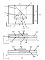
発振素子の一実施形態について、図1、図2及び図3を用いて説明する。図1は、発振素子100の外観を示す斜視図で、図2(a)は発振素子100の上面図、図2(b)、(c)はそれぞれ図2(a)のA−A’線、B−B’線における発振素子100の断面図である。また、図3は、複数の変形例のアンテナ部102の整合領域110の上面図である。
Hereinafter, embodiments and examples of the present invention will be described with reference to the drawings.
(Embodiment)
An embodiment of an oscillation element will be described with reference to FIGS. FIG. 1 is a perspective view showing an appearance of the
本実施形態の発振素子100は、共振部101とアンテナ部102で構成される。共振部101は、電磁波利得を有する活性層103、第一の導体層104、第二の導体層105から構成される。アンテナ部102は、第三の導体層106、第四の導体層107から構成される。共振部101は、基板108上に集積されており、共振部101の側部には層間絶縁膜109が配置された構成となっている。共振部101は、第一の導体層104と第二の導体層105とをクラッドとして、この近接した二枚の導体板でコアの活性層103を挟んだDMWと呼ばれるプラズモン導波路である。この共振部の第一の導体層と第二の導体層は、誘電率実部が負の負誘電率媒質を含むプラズモン導波路構造を構成する。
The
活性層103は、キャリアのサブバンド間遷移によりテラヘルツ波を発生する多重量子井戸構造の半導体部を含んでおり、テラヘルツ波の周波数領域における電磁波利得を有している。活性層103は、例えば、数十層の半導体多層膜からなる共鳴トンネル構造や、数百から数千層の半導体多層膜からなる量子カスケードレーザ構造などが好適である。本実施形態では、活性層103として、共鳴トンネルダイオード(以下、RTDとも記す)を用いた。RTDは、微分負性抵抗領域においてフォトンアシストトンネル現象に基づくミリ波からテラヘルツ波の周波数領域の電磁波利得を有する。活性層103は、多重量子井戸構造の半導体部と第一の導体層104及び第二の導体層105を接続するために高濃度にドーピングした半導体層を備えてもよい。上記積層構造を有する活性層103により、その積層方向が規定される。
The
活性層103と第一の導体層104及び第二の導体層105とは、それぞれ、機械的かつ電気的に互いに接している。発振素子100は、第一の導体層104と第二の導体層105との間に外部電源からバイアスを印加することで、活性層103のRTDにバイアスを印加する構成となっている。ここで、第一の導体層104と第二の導体層105は、金属(Ag、Au、Cu、Al、AuIn合金など)、半金属(Bi、Sb、ITO、ErAsなど)、高濃度にドーピングされた半導体などを好適に用いることができる。
The
本実施形態の発振素子100は、電磁波の出射する共振部101の端面に第三の導体層106と第四の導体層107からなるアンテナ部102を備えている。図1、図2の構成では第三の導体層106と第四の導体層107の間に層間絶縁膜109が配置される。第三の導体層106は第一の導体層104と、さらに第四の導体層107は第二の導体層105と電気的に接続する。図1及び図2では第一の導体層104と第三の導体層106は同時に形成され、電気的に接続されている。また、第二の導体層105と第四の導体層107も同時に形成され、電気的に接続されている。共振器101とアンテナ部102の間において、第三の導体層と第四の導体層は上記膜の積層方向に重なる整合領域110を備え、整合領域110は共振部101からアンテナ部102に向かって伸長する方向に領域の幅を徐々に小さくしている。つまり、整合領域110は、共振部からアンテナ部への方向に、導体層の積層方向から見て先細りしたテーパー状を有する。
The
整合領域110の幅を徐々に小さくすることによって整合領域110内での電磁波の反射を低減させ、電磁波の減衰を抑えることができる。整合領域110の共振部101に接する部分の幅111を変更することにより、アンテナ部102の入力インピーダンスを調整できる。これにより共振部101の特性インピーダンスとアンテナ部102の入力インピーダンスを近接させ、インピーダンス整合をとることができる。共振部101から出射した電磁波は出射直後には膜の積層方向(図2(a)の紙面に垂直方向)の電界成分を持っている。電磁波は整合領域110を通過し、アンテナ部102を進むことによって電界が90度回転し、偏光方向が図2(a)の紙面の面内方向の方向へと変わる。偏光方向を変えることにより、半導体プロセス等で容易に形成できる平面型のアンテナを構成することができる。すなわち、アンテナ部102は、2つの導体層である第三の導体層と第四の導体層がそれぞれ異なる層にて形成される平面型アンテナである。また、アンテナ部102はテーパースロットアンテナなどのアンテナを形成して、自由空間などの外部との整合をとることにより、共振部101内の電磁波を効率的に利用できる発振素子100を得ることができる。
By gradually reducing the width of the
図4に整合領域110の幅111を変化させた場合の電磁波の出力を計算した結果を示す。計算にはアンシスジャパン(株)のHFSSを用いた。図4のグラフの結果を得た構成では、共振部101には後述の実施例1と同じ構造と材料を用い、テーパースロットアンテナの開放端の幅を500μm、テーパー角112を20度とした。なお、後述する実施例1で説明する様に、この共振部201の幅は4μmである。また、図2(a)においては、見易くするために、テーパー角112、共振部201の幅と整合領域110の幅111との比率、テーパースロットアンテナの開放端の幅と整合領域110の幅111との比率などは実際のものとは異なるように描かれている(このことは他の図面でもほぼ同様である)。この構成では、共振部の特性インピーダンスは1Ω以下と小さいため、図4から分かる様に、入力インピーダンスが整合するための整合領域110の幅111は100μmから200μm付近が好ましい。共振器の端面からの反射を利用して電磁波を定在化するファブリペロー型の共振器構造を共振部101に有するため、共振部101と整合領域110の界面では完全にインピーダンス整合せずに、一部電磁波を反射させる必要がある。ここで、第一の導体層104、第二の導体層105、第三の導体層106及び第四の導体層107は、導電率の高い部材、例えば金属、半金属、高濃度にドーピングされた半導体、またはこれらの材料から適宜選択された材料を含む積層した導電部材で構成されるのが好ましい。
FIG. 4 shows the calculation result of the electromagnetic wave output when the
以上の構成は適宜変更して受信素子などとして用いることも可能で、アンテナ部102は、発振アンテナだけでなく、受信アンテナとして機能させることもできる。
こうした受信素子は、電磁波を共振させるための共振部と、共振部の端面に設けられて共振部へと電磁波を入射させるための2つの導体層を含む積層構造を有したアンテナ部と、を備える。ここでも、整合領域は、共振部からアンテナ部に向かって伸長する方向に前記積層方向から見て先細りしたテーパー状を有する。
The above configuration can be changed as appropriate to be used as a receiving element or the like, and the
Such a receiving element includes a resonating part for resonating electromagnetic waves, and an antenna part having a laminated structure including two conductor layers provided on the end face of the resonating part for allowing electromagnetic waves to enter the resonating part. . Again, the matching region has a taper shape that tapers in a direction extending from the resonance portion toward the antenna portion when viewed from the stacking direction.
また、整合領域110の形状は、図2(a)や図3(a)の通りの直線的な構成だけでなく、図3(b)で示す様な曲線での構成や、図3(c)で示す様な電磁波の波長の半分λ/2以下の長さの段差を設けてもよい。すなわち、整合領域110の積層方向から見た形状は上述の形状に必ずしも限定されるものではなく、共振部101からアンテナ部102に向かって伸長する方向に整合領域110の幅が徐々に小さくなる構造であればよい。ここで、「徐々に」とは、単調に連続的であってもよいし、非連続的であってもよく、また多少の幅の増減部分を交えてもよい。
Further, the shape of the
また、図1、図2では、整合領域110の第三の導体層106と第四の導体層107で挟まれる部分は層間絶縁膜109で構成されているが、導電部材でなければよく、利得媒質または誘電体や空間などの絶縁層で構成してもよい。さらに図では、対向する2つの導体層は平行に描いてあるが、必ずしも平行でなくてもよい。また、アンテナ部の第三の導体層106と第四の導体層107は、共振部からアンテナ部への方向に伸びる共振部の中心線を挟んで対称に描いてあるが、これも必ずしも対称でなくてもよい。作製の都合上や要求される仕様に応じて、適宜の設計が可能である。
In FIG. 1 and FIG. 2, the portion sandwiched between the
以上で説明した様に、本実施形態によれば、電磁波が共振する共振部と電磁波が出射または入射するアンテナ部との間の界面からアンテナ部側に伸びて、共振部とアンテナ部の境界での電磁波の反射を抑えるための整合領域を備える。この整合領域は、アンテナ部を形成する第三の導体層と第四の導体層が利得媒質または誘電体などを介して膜の積層方向に重なっている。そして、この整合領域の面積や形状などを変更することにより、アンテナ部の入力インピーダンスを調整でき、共振部の特性インピーダンスとアンテナ部の入力インピーダンスを近接させ、インピーダンス整合をとることができる。また、共振部からアンテナ部に向かって伸長する方向に沿って整合領域の幅を徐々に小さくし、更に第三の導体層と第四の導体層で開口アンテナを形成することで、自由空間などの外部との整合をとることができる。すなわち、例えば、電磁波を自由空間に放射する出射端を有し、アンテナ部が、電磁波の伝播の方向に整合領域のテーパー状の幅を徐々に小さくして前記出射端において自由空間に整合するようにした開口アンテナを構成することができる。これにより、シリコンレンズなどの追加部品を削減することができ、コストを下げることができる。また、平面アンテナ構造を採用できるため、簡便な作製方法で機械的に安定した、電磁波を効率的に利用できる発振素子や受信素子等の素子が実現できる。 As described above, according to the present embodiment, the interface extends between the resonance part where the electromagnetic wave resonates and the antenna part where the electromagnetic wave is emitted or incident, toward the antenna part, and at the boundary between the resonance part and the antenna part. A matching region for suppressing reflection of electromagnetic waves is provided. In this matching region, the third conductor layer and the fourth conductor layer forming the antenna portion overlap each other in the film stacking direction via a gain medium or a dielectric. By changing the area and shape of the matching region, the input impedance of the antenna unit can be adjusted, and the impedance impedance matching can be achieved by bringing the characteristic impedance of the resonance unit close to the input impedance of the antenna unit. In addition, by gradually reducing the width of the matching region along the direction extending from the resonance portion toward the antenna portion, and further forming an aperture antenna with the third conductor layer and the fourth conductor layer, free space, etc. Can be consistent with the outside. That is, for example, it has an exit end that radiates electromagnetic waves into free space, and the antenna unit gradually matches the free space at the exit end by gradually reducing the tapered width of the matching region in the propagation direction of the electromagnetic waves. An aperture antenna can be configured. Thereby, additional parts, such as a silicon lens, can be reduced and cost can be reduced. In addition, since a planar antenna structure can be adopted, an element such as an oscillation element or a reception element that can be used mechanically and can efficiently use electromagnetic waves can be realized by a simple manufacturing method.
以下、より具体的な実施例を説明する。
(実施例1)
本発明の発振素子の具体的な実施例1について、図5と図6を用いて説明する。図5は本実施例の斜視図で、図6は上面図である。本実施例では、活性層203として、サブバンド間遷移によりテラヘルツ波を発生するInGaAs/InAlAs系の3重障壁共鳴トンネルダイオード(RTD)構造を含む半導体積層構造を用いた。RTD構造は、n−InGaAs(厚さ50nm、Si、キャリア濃度2×1018cm−3)、InGaAs(5nm)、AlAs(1.3nm)、InGaAs(7.6nm)、InAlAs(2.6nm)、InGaAs(5.6nm)、AlAs(1.3nm)、InGaAs(5nm)、n−InGaAs(50nm、Si、2×1018cm−3)の順に積層された半導体量子井戸構造である。RTD構造の上下に配置された高濃度にキャリアドープしたn+InGaAs(400nm、1×1019cm−3)により、RTD構造と第一の導体層204及び第二の導体層205とを比較的低抵抗で接続する。
Hereinafter, more specific examples will be described.
Example 1
A specific example 1 of the oscillation element of the present invention will be described with reference to FIGS. FIG. 5 is a perspective view of the present embodiment, and FIG. 6 is a top view. In this embodiment, a semiconductor multilayer structure including an InGaAs / InAlAs triple barrier resonant tunnel diode (RTD) structure that generates terahertz waves by intersubband transition is used as the
本実施例では、第一の導体層204と第三の導体層206は同時に形成され、Ti/Pd/Au/Pd/Ti(各部の厚さ=20nm/20nm/400nm/20nm/20nm)の積層膜で構成される。第二の導体層205と第四の導体層207も同時に形成され、Ti/Pd/Au(各部の厚さ=20nm/20nm/400nm)の積層膜で構成される。基板208は、半絶縁性GaAs基板であり、第一の導体層204と機械的に接続されている。層間絶縁膜209は、テラヘルツ帯で低損失な絶縁材料(例えばBCBなどの樹脂やSiO2などの無機材料)が好適であり、本実施例ではBCB(ベンゾシクロブテン)を用いている。発振素子200は、第一の導体層204と第二の導体層205に接続された配線(不図示)を介して電源に接続され、駆動用のバイアス電圧が活性層203に供給される。
In this embodiment, the
共振部201は、ファブリペロー型の共振器構造であり、電磁波の伝播方向において少なくとも二つの端面を備えている。この端面からの反射を利用して電磁波を定在化するので、伝播方向の長さが発振波長を決める要素となる。本実施例では、共振部201の長さを管内波長λgの1/2倍となる50μm、幅を4μmとした。第一の導体層204と第二の導体層205との積層方向の距離は、略1μmと近接している。すなわち、共振部の第一の導体層と第二の導体層は、導波路構造の導波モードないし発振素子の発振モードにおける電磁波の管内波長以下の距離に近接する。共振部201は、発振周波数を0.2THz、管内波長λgを100μmとして設計されている。電磁波は、共振部201内をプラズモンモードで伝播し、共振部201の端面が開放端となる。発振素子200は、微分負性抵抗領域におけるフォトンアシストトンネル現象に基づいて発生した0.2THzの電磁波を、共振部201の端に配置されたアンテナ部202から放射する。
The resonating
アンテナ部202において、共振部との界面から伸びて、電磁波の反射を低減するために整合領域210を形成している。整合領域210では、第三の導体層206と第四の導体層207が層間絶縁膜209を介して膜の成長方向に重なっている。本実施例の整合領域210の形状は、共振部201に接した部分の幅211の寸法が100μm、テーパー角度212は20度とした。整合領域210の共振部201に接した部分の幅211を変更することにより、アンテナ部202の入力インピーダンスを調整でき、共振部201との整合をとることができる。具体的には、整合領域210の幅211の寸法を大きくすることにより、アンテナ部202の入力インピーダンスを小さくできる。更に、第三の導体層206と第四の導体層207の面内方向の間隔を電磁波の伝播方向に徐々に広げることにより、自由空間との整合をとることができる。本実施例のアンテナ部202はテーパースロットアンテナ構造を構成しており、その最大開口部の幅は略700μmとした。
In the
本実施例の作製方法は例えば以下の工程を有する。基板208として半絶縁性GaAs基板を準備し、半絶縁性GaAs基板208上に金属層Ti/Pd/Au(各部の厚さ=20nm/20nm/200nm)を蒸着装置にて形成する。また、前述のRTD構造と高濃度にキャリアドープしたn−InGaAsをエピタキシャル成長させたInP基板上に、金属層Ti/Pd/Au(各部の厚さ=20nm/20nm/200nm)を蒸着装置にて形成する。前記InP基板と基板208の上面を対向させて、Auの熱圧着法で2枚の基板を接合する。ここで、圧着接合により形成したTi/Pd/Au/Pd/Ti(各部の厚さ=20nm/20nm/400nm/20nm/20nm)を後述の工程で加工すると第一の導体層204及び第三の導体層206となる。塩酸エッチングにより、接合で一体化した基板からInP基板を除去して、半導体層を基板208に転写する。フォトリソグラフィーとドライエッチング法により、半導体層を導波路形状に加工し、活性層203を形成する。さらに圧着接合により形成したTi/Pd/Au/Pd/Tiをフォトリソグラフィーとドライエッチング法により、第一の導体層204と第三の導体層206に加工する。スピンコート法により層間絶縁膜209で活性層203の構造の埋め込みを行い、ドライエッチング法で活性層203の上部を露出させる。層間絶縁膜にはBCBを用いた。そして、真空蒸着法とリフトオフ法を用いて、Ti/Pd/Au(各部の厚さ=20nm/20nm/200nm)からなる第二の導体層205と第四の導体層207を形成する。
The manufacturing method of this example includes the following steps, for example. A semi-insulating GaAs substrate is prepared as the
これにより、シリコンレンズなどの追加部品を使用することなく、簡便な作製方法で、電磁波を利用できる発振素子などが実現できる。また、この構造を用いれば共振器とアンテナ部の整合性を簡便に設計及び達成できる。 As a result, it is possible to realize an oscillation element or the like that can use electromagnetic waves by a simple manufacturing method without using an additional component such as a silicon lens. Further, if this structure is used, the matching between the resonator and the antenna portion can be designed and achieved easily.
本発明は、上記構成に限定されるものでない。例えば、本実施例では、活性層201として、InP基板上に成長したInGaAs/InAlAs、InGaAs/AlAsからなる3重障壁共鳴トンネルダイオードについて説明してきた。しかし、これらの構造や材料系に限られることなく、他の構造や材料の組み合わせであっても本発明に係る発振素子などの導波路を提供することができる。例えば、2重障壁量子井戸構造を有する共鳴トンネルダイオードや、4重以上の多重障壁量子井戸を有する共鳴トンネルダイオード、量子カスケードレーザで知られるようなカスケード接続された多重量子井戸構造などを用いてもよい。RTDを用いた発振素子200では共振部201を構成する2層の導体層の間隔が狭く特性インピーダンスが小さいため、整合領域210の幅211が広くなる。また、量子カスケードレーザで共振部201を構成する場合、共振部201を構成する2層の導体層の間隔が広く特性インピーダンスが大きいため、RTDを共振部とした場合より整合領域210の幅211が狭くなる。
The present invention is not limited to the above configuration. For example, in the present embodiment, a triple barrier resonant tunnel diode made of InGaAs / InAlAs and InGaAs / AlAs grown on an InP substrate has been described as the
これらの構造と材料は、所望される電磁波の周波数などに応じて適宜選定すればよい。また、基板208の材料は用途に応じて選定すればよく、高抵抗シリコン基板、半絶縁性ガリウムヒ素基板、半絶縁性インジウムヒ素基板、半絶縁性ガリウムリン基板などの半導体基板や、ガラス基板、セラミック基板、樹脂基板などを用いてもよい。また、層間絶縁膜209には、SiO2、ポリシリコン、SiNx、AlN、TiO2などの無機材料や、BCB(ベンゾシクロブテン)、SU−8、ポリイミドなどの有機材料が好適に用いられる。更に、低導電性の真性半導体を再成長したものを用いてもよい。また、アンテナ部202はV字アンテナ、ロンビックアンテナ、テーパースロットアンテナ、ビバルディアンテナなどが好適に用いられる。
These structures and materials may be appropriately selected according to the desired frequency of electromagnetic waves. In addition, the material of the
(実施例2)
本発明の実施例2である発振素子300について、図7を用いて説明する。図7は素子の斜視図である。第一の基板303上に形成された共振部301は実施例1と同じRTD構造を用いている。また、その他の構成材料は基板を除き実施例1と同じものを用い、製造方法も共振部301の作製までは実施例1と同じ製造方法で作製した。ここで、基板は第一の基板303、第二の基板304ともに高抵抗シリコン基板を用いている。また、実施例1で述べたように、第一の基板303及び第二の基板304は、半導体、誘電体若しくは絶縁性材料であればシリコンに限らない。その後、層間絶縁膜305で活性層306の構造の埋め込みを行い、ドライエッチング法で活性層306の上部を露出させ、第二の導体層308を形成する。また、アンテナ部302の第三の導体層309と共振部の第一の導体層307は実施例1と同様に同時形成されている。アンテナ部302の第四の導体層310のパターンは第二の接合電極312も兼ねている。第四の導体層310形成と同時に第一の接合電極311も形成する。接合用金バンプ314を第一の接合電極311と第二の接合電極312上に形成し、第一の基板303と第二の基板304を対向させ、接合する。この様にして、アンテナ部は、第一の基板、2つの導体層の一方である第三の導体層、層間絶縁膜、2つの導体層の他方である第四の導体層、第二の基板の順に重なって構成される。
(Example 2)
An
本実施例の整合領域313は、第三の導体層309と第四の導体層310が大気を介して重なっている。また、本実施例のアンテナ部302はビバルディアンテナ構造を構成しているため、整合領域313の形状は図3(b)で示すような曲線での構成を用い、共振部301からアンテナ部302に向かって伸長する方向に整合領域313の幅を徐々に小さくしている。この構造を用いれば、アンテナ部の上下に基板を有するため、片側のみ基板を有する場合と比較して、電磁波を上下対称に放射させることができる。また、共振器とアンテナ部の整合性を簡便に設計及び達成できる。
In the matching region 313 of this embodiment, the
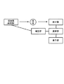
また、これまで説明してきた素子を用い、検体の状態などを算出する演算部などと組合せた図8に示す装置を提供することができる。例えば、上記発振素子を発振器として用い、発振器の端部に検体を配置する。検体は導波路から発振される電磁波と相互作用するため、発振された電磁波は何らかの影響をうける。検体に照射された電磁波は反射や透過するため、それを検出器で検出する。上記受信素子を検出器として用いることもできる。その後、パソコン等の演算部で、検出した信号から検体の情報(状態など)を算出する。具体的には、薬の状態などを検査する産業用検査装置などの応用が想定される。以上の様にして、発振素子から出射した電磁波が照射された検体からの電磁波を受信素子で検出する測定装置を構成することができる。ここでは、発振素子と受信素子のうちの少なくとも一方が、本発明の発振素子または受信素子であり、検体と相互作用した電磁波を検出し、検出した信号から検体の情報を取得する。 In addition, the apparatus shown in FIG. 8 can be provided in which the element described so far is used and combined with a calculation unit that calculates the state of the specimen and the like. For example, the oscillation element is used as an oscillator, and a specimen is placed at the end of the oscillator. Since the specimen interacts with the electromagnetic wave oscillated from the waveguide, the oscillated electromagnetic wave is affected in some way. Since the electromagnetic wave irradiated to the specimen is reflected or transmitted, it is detected by a detector. The receiving element can also be used as a detector. Thereafter, the information (state and the like) of the specimen is calculated from the detected signal by a calculation unit such as a personal computer. Specifically, an application such as an industrial inspection apparatus that inspects the state of a medicine or the like is assumed. As described above, it is possible to configure a measuring apparatus that detects an electromagnetic wave from a specimen irradiated with an electromagnetic wave emitted from an oscillation element by a receiving element. Here, at least one of the oscillating element and the receiving element is the oscillating element or the receiving element of the present invention, detects an electromagnetic wave interacting with the specimen, and acquires information on the specimen from the detected signal.
以上、本発明の実施形態と実施例について説明したが、本発明はこれらの実施形態と実施例に限定されず、その要旨の範囲内で種々の変形及び変更が可能である。 As mentioned above, although embodiment and the Example of this invention were described, this invention is not limited to these embodiment and Example, A various deformation | transformation and change are possible within the range of the summary.
100:発振素子(受信素子)、101:共振部、102:アンテナ部、103:活性層(コア層、利得媒質)104:第一の導体層、105:第二の導体層、106:第三の導体層、107:第四の導体層、108:基板、109:層間絶縁膜(絶縁体)、110:整合領域、111:整合領域の幅、112:整合領域のテーパー角 DESCRIPTION OF SYMBOLS 100: Oscillation element (receiving element), 101: Resonance part, 102: Antenna part, 103: Active layer (core layer, gain medium) 104: First conductor layer, 105: Second conductor layer, 106: Third 107: fourth conductor layer, 108: substrate, 109: interlayer insulating film (insulator), 110: matching region, 111: width of matching region, 112: taper angle of matching region
Claims (13)
前記共振部の端面に設けられて前記共振部から前記電磁波を出射させるための2つの導体層を含む積層構造を有したアンテナ部と、
を備えた電磁波を発振する発振素子であって、
前記2つの導体層は、前記積層構造の積層方向に間隔を隔てて少なくとも一部が重なるインピーダンス整合に係る整合領域を有し、
前記整合領域は、前記共振部から前記アンテナ部に向かって伸長する方向に前記積層方向から見て先細りしたテーパー状を有することを特徴とする発振素子。 A resonating part for resonating electromagnetic waves;
An antenna portion having a laminated structure including two conductor layers provided on an end face of the resonance portion for emitting the electromagnetic wave from the resonance portion;
An oscillation element that oscillates electromagnetic waves,
The two conductor layers have a matching region related to impedance matching that overlaps at least partially with a gap in the stacking direction of the stacked structure,
The oscillation region is characterized in that the matching region has a taper shape that is tapered when viewed from the stacking direction in a direction extending from the resonance portion toward the antenna portion.
前記アンテナ部の2つの導体層は、利得媒質または絶縁体を介して少なくとも一部が重なって整合領域を構成することを特徴とする請求項1に記載の発振素子。 The resonance part is configured by laminating a first conductor layer, a gain medium having a gain with respect to electromagnetic waves, and a second conductor layer in this order,
2. The oscillation element according to claim 1, wherein the two conductor layers of the antenna section at least partially overlap with each other via a gain medium or an insulator to form a matching region.
前記アンテナ部は、電磁波の伝播の方向に前記整合領域のテーパー状の幅を徐々に小さくして前記出射端において自由空間に整合するようにした開口アンテナであることを特徴とする請求項1から7の何れか1項に記載の発振素子。 An emission end that radiates electromagnetic waves oscillated in the oscillation element to free space;
2. The aperture antenna according to claim 1, wherein the antenna section is an aperture antenna in which a tapered width of the matching region is gradually reduced in the direction of propagation of electromagnetic waves so as to match with free space at the emission end. 8. The oscillation element according to any one of 7 above.
前記共振部の端面に設けられて前記共振部へと前記電磁波を入射させるための2つの導体層を含む積層構造を有したアンテナ部と、
を備えた電磁波を検出する受信素子であって、
前記2つの導体層は、前記積層構造の積層方向に間隔を隔てて少なくとも一部が重なるインピーダンス整合に係る整合領域を有し、
前記整合領域は、前記共振部から前記アンテナ部に向かって伸長する方向に前記積層方向から見て先細りしたテーパー状を有することを特徴とする受信素子。 A resonating part for resonating electromagnetic waves;
An antenna unit having a laminated structure including two conductor layers provided on an end surface of the resonance unit and allowing the electromagnetic wave to enter the resonance unit;
A receiving element for detecting electromagnetic waves, comprising:
The two conductor layers have a matching region related to impedance matching that overlaps at least partially with a gap in the stacking direction of the stacked structure,
The matching element has a tapered shape that tapers in a direction extending from the resonance unit toward the antenna unit when viewed from the stacking direction.
前記発振素子と前記受信素子のうちの少なくとも一方が、請求項1から11の何れか1項に記載の発振素子、または請求項12に記載の受信素子であり、
検体と相互作用した前記電磁波を検出し、検出した信号から検体の情報を取得することを特徴とする装置。 A measuring device for detecting an electromagnetic wave from a specimen irradiated with an electromagnetic wave emitted from an oscillation element by a receiving element,
At least one of the oscillation element and the reception element is the oscillation element according to any one of claims 1 to 11, or the reception element according to claim 12.
An apparatus for detecting the electromagnetic wave interacting with a specimen and acquiring information on the specimen from the detected signal.
Priority Applications (3)
| Application Number | Priority Date | Filing Date | Title |
|---|---|---|---|
| JP2012108683A JP2013236326A (en) | 2012-05-10 | 2012-05-10 | Oscillation element, reception element, and measuring apparatus |
| US14/387,152 US20150303559A1 (en) | 2012-05-10 | 2013-04-19 | Oscillation device, reception device and sample information acquisition apparatus |
| PCT/JP2013/062308 WO2013168596A1 (en) | 2012-05-10 | 2013-04-19 | Oscillation device, reception device and sample information acquisition apparatus |
Applications Claiming Priority (1)
| Application Number | Priority Date | Filing Date | Title |
|---|---|---|---|
| JP2012108683A JP2013236326A (en) | 2012-05-10 | 2012-05-10 | Oscillation element, reception element, and measuring apparatus |
Publications (2)
| Publication Number | Publication Date |
|---|---|
| JP2013236326A true JP2013236326A (en) | 2013-11-21 |
| JP2013236326A5 JP2013236326A5 (en) | 2015-06-25 |
Family
ID=48446573
Family Applications (1)
| Application Number | Title | Priority Date | Filing Date |
|---|---|---|---|
| JP2012108683A Pending JP2013236326A (en) | 2012-05-10 | 2012-05-10 | Oscillation element, reception element, and measuring apparatus |
Country Status (3)
| Country | Link |
|---|---|
| US (1) | US20150303559A1 (en) |
| JP (1) | JP2013236326A (en) |
| WO (1) | WO2013168596A1 (en) |
Cited By (1)
| Publication number | Priority date | Publication date | Assignee | Title |
|---|---|---|---|---|
| CN106299635A (en) * | 2015-05-25 | 2017-01-04 | 深圳光启高等理工研究院 | Antenna |
Families Citing this family (7)
| Publication number | Priority date | Publication date | Assignee | Title |
|---|---|---|---|---|
| JP2014207654A (en) | 2013-03-16 | 2014-10-30 | キヤノン株式会社 | Waveguide element |
| US9899959B2 (en) | 2015-05-22 | 2018-02-20 | Canon Kabushiki Kaisha | Element, and oscillator and information acquiring device including the element |
| CN107946765A (en) * | 2017-11-21 | 2018-04-20 | 南京濠暻通讯科技有限公司 | A kind of high-gain Vivaldi array antennas for loading director |
| US10897073B2 (en) | 2018-08-27 | 2021-01-19 | Canon Kabushiki Kaisha | Receiver for detecting a terahertz wave and image forming apparatus |
| JP7395281B2 (en) | 2019-08-23 | 2023-12-11 | キヤノン株式会社 | element |
| US11637530B2 (en) | 2021-02-17 | 2023-04-25 | Canon Kabushiki Kaisha | Oscillating element |
| CN113889745B (en) * | 2021-09-30 | 2022-05-03 | 北京星英联微波科技有限责任公司 | Compact broadband circularly polarized antenna |
Citations (2)
| Publication number | Priority date | Publication date | Assignee | Title |
|---|---|---|---|---|
| JP2010093062A (en) * | 2008-10-08 | 2010-04-22 | Canon Inc | Terahertz wave generating element |
| JP2011024176A (en) * | 2009-07-14 | 2011-02-03 | Keycom Corp | Electromagnetic wave transfer unit for dielectric waveguide |
Family Cites Families (5)
| Publication number | Priority date | Publication date | Assignee | Title |
|---|---|---|---|---|
| JP3146260B2 (en) * | 1999-03-05 | 2001-03-12 | 郵政省通信総合研究所長 | Planar radiation type oscillation device |
| US7177515B2 (en) | 2002-03-20 | 2007-02-13 | The Regents Of The University Of Colorado | Surface plasmon devices |
| FR2908931B1 (en) | 2006-11-21 | 2009-02-13 | Centre Nat Rech Scient | INTEGRATED TERAHERTZ ANTENNA AND TRANSMITTER / RECEIVER, AND PROCESS FOR THEIR MANUFACTURE. |
| JP5441470B2 (en) * | 2009-03-27 | 2014-03-12 | キヤノン株式会社 | Resonator |
| JP5612842B2 (en) * | 2009-09-07 | 2014-10-22 | キヤノン株式会社 | Oscillator |
-
2012
- 2012-05-10 JP JP2012108683A patent/JP2013236326A/en active Pending
-
2013
- 2013-04-19 WO PCT/JP2013/062308 patent/WO2013168596A1/en active Application Filing
- 2013-04-19 US US14/387,152 patent/US20150303559A1/en not_active Abandoned
Patent Citations (2)
| Publication number | Priority date | Publication date | Assignee | Title |
|---|---|---|---|---|
| JP2010093062A (en) * | 2008-10-08 | 2010-04-22 | Canon Inc | Terahertz wave generating element |
| JP2011024176A (en) * | 2009-07-14 | 2011-02-03 | Keycom Corp | Electromagnetic wave transfer unit for dielectric waveguide |
Non-Patent Citations (1)
| Title |
|---|
| BENJAMIN S. WILLIAMS, SUSHIL KUMAR, HANS CALLEBAUT, QING HU, AND JOHN L. RENO: "Terahertz quantum-cascade laser at λ.100 μ m using metal waveguide for mode confinement", APPLIED PHYSICS LETTERS, vol. 83, no. 11, JPN7016001115, 15 September 2003 (2003-09-15), pages 2124 - 2126, XP012035076, ISSN: 0003313032, DOI: 10.1063/1.1611642 * |
Cited By (1)
| Publication number | Priority date | Publication date | Assignee | Title |
|---|---|---|---|---|
| CN106299635A (en) * | 2015-05-25 | 2017-01-04 | 深圳光启高等理工研究院 | Antenna |
Also Published As
| Publication number | Publication date |
|---|---|
| US20150303559A1 (en) | 2015-10-22 |
| WO2013168596A1 (en) | 2013-11-14 |
Similar Documents
| Publication | Publication Date | Title |
|---|---|---|
| JP6034616B2 (en) | Waveguide, manufacturing method thereof, and electromagnetic wave analyzer | |
| US9391428B2 (en) | Waveguide element | |
| JP2013236326A (en) | Oscillation element, reception element, and measuring apparatus | |
| JP6478220B2 (en) | Terahertz device and terahertz integrated circuit | |
| US8805147B2 (en) | Waveguide, apparatus including the waveguide, and method of manufacturing the waveguide | |
| US7884767B2 (en) | Antenna device | |
| JP5028068B2 (en) | Active antenna oscillator | |
| JP6137781B2 (en) | Waveguide, device using the waveguide, and waveguide manufacturing method | |
| US20120274410A1 (en) | Oscillator | |
| JP2014158254A (en) | Electromagnetic wave generating element and detection element | |
| JP5441470B2 (en) | Resonator | |
| JP2009059922A (en) | Laser device | |
| JP5590879B2 (en) | Generating element and semiconductor element | |
| JP2016158023A (en) | Terahertz element | |
| JP6893591B1 (en) | Laser module | |
| JP2008306523A (en) | Oscillator | |
| JP6719882B2 (en) | Oscillation element and measuring device using the same | |
| JP5417199B2 (en) | Oscillating element | |
| US9438168B2 (en) | Oscillator | |
| JP2016219796A (en) | Element, and oscillator and information acquisition device including the element |
Legal Events
| Date | Code | Title | Description |
|---|---|---|---|
| A521 | Request for written amendment filed |
Free format text: JAPANESE INTERMEDIATE CODE: A523 Effective date: 20150508 |
|
| A621 | Written request for application examination |
Free format text: JAPANESE INTERMEDIATE CODE: A621 Effective date: 20150508 |
|
| A977 | Report on retrieval |
Free format text: JAPANESE INTERMEDIATE CODE: A971007 Effective date: 20160317 |
|
| A131 | Notification of reasons for refusal |
Free format text: JAPANESE INTERMEDIATE CODE: A131 Effective date: 20160510 |
|
| A02 | Decision of refusal |
Free format text: JAPANESE INTERMEDIATE CODE: A02 Effective date: 20161108 |